MMB Research Z357PA20 ZIGBEE RADIO MODULE User Manual
MMB Research Inc. ZIGBEE RADIO MODULE
UserManual.wiki
>
MMB Research
>
Z357PA20 User Manual
User Manual
Navigation menu
Upload a User Manual
Namespaces
Wiki Guide
HTML
PDF
Info
Views
User Manual
Discussion / Help
Navigation

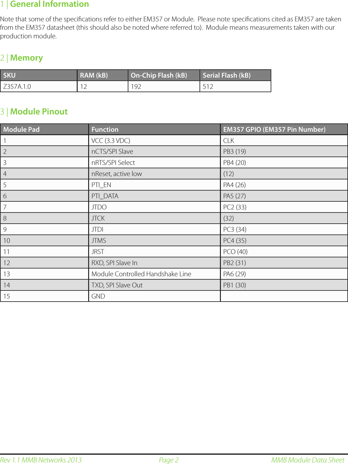
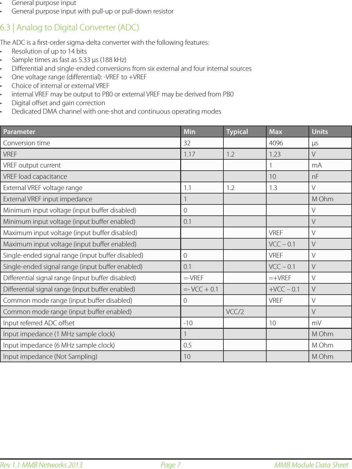
![Page 3Rev 1.1 MMB Networks 2013 MMB Module Data Sheet3.1 | Debug and Programming InterfaceIn order to access the EM357 for programming and debug purposes, it is recommended that the designer incorporate Ember’s 10-pin InSight Port connector. This will allow Ember’s InSight Adapter (ISA3) to be used. Contact Ember for details regarding the InSight Port connector and ISA3. The following table shows a pin mapping between Ember’s 10-pin InSight Port connector and the module, and the graphic to the right displays the layout of the InSight Port connector.4 | Electrical Specications4.1 | Absolute Maximum Ratings4.2 | Recommended Operating ConditionsEmber InSight Port Pin Module Pin1 10, 18 (VCC)2 25 (PC2 / JTDO / SWO)3 28 (PC0 / JRST)4 26 (PC3 / JTDI)5 1, 11, 19, 22, 32 (GND)6 24 (JTCK)7 27 (PC4 / JTMS / SWDIO)8 17, 23 (nReset)9 7 (PA4/PTI_EN)10 6 (PA5/PTI_DATA)Parameter Minimum Maximum UnitsSupply Voltage (VCC) 0 3.6 VVoltage on any GPIO ([PA[0:7], PB[0:7], PC[0:7]), JTCK, nReset -0.3 VCC + 0.3 VVoltage on any GPIO pin (PA4, PA5, PB5, PB6, PB7, PC1) when used as an input to the general purpose ADC with the low voltage range selected -0.3 2 VAmbient Operating Temperature -40 85 °CParameter Minimum Typical Maximum UnitsSupply Voltage (VCC) 2.7 3.3 3.6 VTemperature Range -40 85 °C1 23 45 67 89 10VBRDPC0 (nJRST)GNDPC4 (JTMS/SWDIO)PA4 (PTI_EN)PC2 (JTDO/SWO)PC3 (JTDI)JCLK/SWCLKnRESETPA5 (PTI_DATA)](https://usermanual.wiki/MMB-Research/Z357PA20/User-Guide-2029592-Page-3.png)
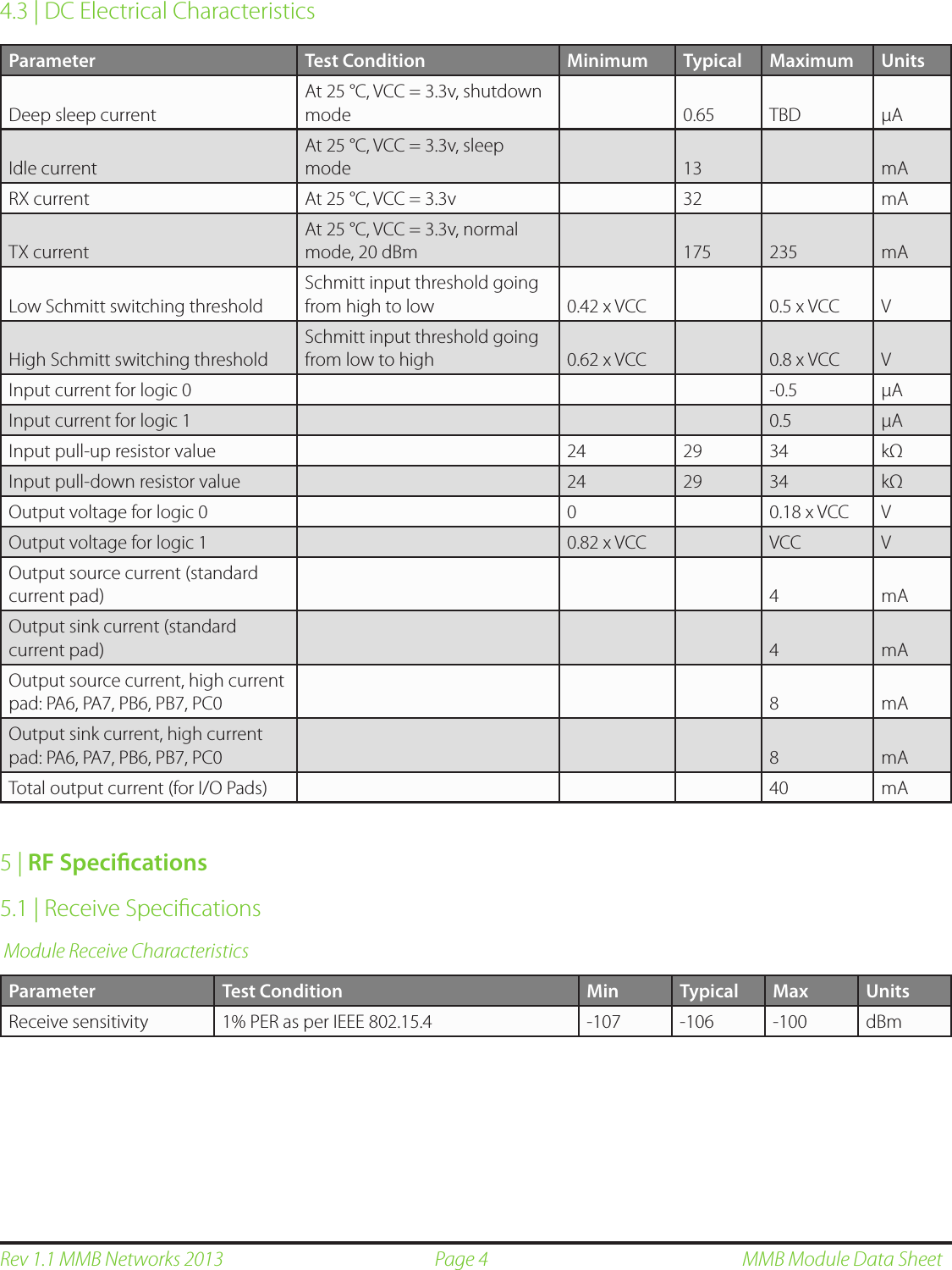
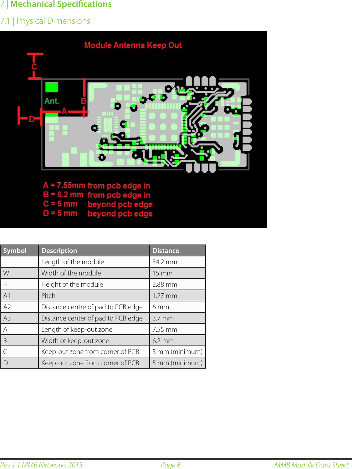
![Page 9Rev 1.1 MMB Networks 2013 MMB Module Data Sheet7.4 | Labelling11mm11mm8 | Soldering Temperature Time Prole for reow soldering (Lead-free solder)150˚C - 190˚C220˚C30 +20/-10s90 ±30s230˚C - 240˚C maxTemp[ ˚C ]Time [ s ]Maximum reflow cycles: 2Opposite-side reflow is prohibited due to the module weight. You must not place the module on the bottom / underside of your PCB and re-flow.](https://usermanual.wiki/MMB-Research/Z357PA20/User-Guide-2029592-Page-9.png)