MXCHIP Information Technology EMW3081 Embedded WiFi Module User Manual DS0005E EMW3162
Shanghai MXCHIP Information Technology Co.,Ltd. Embedded WiFi Module DS0005E EMW3162
user manual
Overview
Features
z Support 802.11 b/g/n standard,Consists of a
Cortex-M3 microcontroller, WLAN MAC,
Base Band and RF.
z 512 KB SRAM ,2 MB SDRAM and 2 MB FLASH
configuration
z Operating Voltage:DC 3.3V
z When uses 20MHz bandwidth, the maximum
transmission rate reached 72.2Mbps
z When uses 40MHz bandwidth, the maximum
transmission rate reached 150Mbps
z Wi-Fi related features
Support 802.11 b/g/n and
compatible
Wi-Fi supports WPS
Support Wi-Fi directly connected
Support Station, Soft AP
Support EasyLink
Having designed for IoT applications
to optimize the TCP/IP protocol
stack
PCB Antenna or IPX Antenna is
optional
z Peripheral:
1x HS UART
1x I2C
1x SPI
1x SWD
4x PWM
Up to 15 GPIOs
z Working environment temperature:
-20℃ to +85℃
Applications:
z Smart LED
z Smart transportation
z Smart home furnishing and intelligent
home appliances
z Instrument
z Medical care
z Industrial automation
z Smart Security
z Smarter Energy
Module model
Product model Antenna model Introduction
EMW3081-P PCB antenna Default
EMW3081-E IPX antenna O
p
tional
Date Sheet
EMW3081
Embedded Wi-Fi module
Version:1.0 Date:2016-2-23 Number:

Copyright statement:
Without permission, prohibition of the use or copying any content of this manual in whole or in part,
and this applies especially to brand, model name, part number and diagram.

1
Content
Overview .................................................................................................................................................................................. 1
1.Product summary ......................................................................................................................................................... 4
1.1.Pinouts ................................................................................................................................................................. 5
1.2.Pins Definition ................................................................................................................................................... 6
2.Electrical Parameters ................................................................................................................................................... 8
2.1Operating Conditions ..................................................................................................................................... 8
2.2Power Parameters ............................................................................................................................................ 8
2.3Operating Environment .................................................................................................................................. 9
2.4ESD ........................................................................................................................................................................ 9
3.RF Parameters .............................................................................................................................................................. 11
3.1.General Specification .................................................................................................................................... 11
4.Antenna Information................................................................................................................................................. 12
4.1.Antenna type ................................................................................................................................................... 12
4.2.PCB antenna design requirements ........................................................................................................... 12
4.3.Approved External Antenna Specification ............................................................................................. 13
4.4.U.F.L RF Connector ......................................................................................................................................... 15
5.The assembly information and manufacturing guidance ............................................................................ 16
5.1.Mechanical dimensions ................................................................................................................................ 16
5.2.Use guidelines(Please read carefully) ...................................................................................................... 17
5.3.The matters needing attention .................................................................................................................. 19
5.4.MSL/Storage Condition ................................................................................................................................ 20
5.5.Recommended Reflow Profile ................................................................................................................... 20
6.Label ................................................................................................................................................................................ 22
7.Firmware encrypt ....................................................................................................................................................... 23
8.FCC Statement ............................................................................................................................................................. 24
9.Sales Information and Technical Support .......................................................................................................... 27
Diagram Content
Figure 2.DIP package dimension ............................................................................................................................... 5
Figure 3. Stamp hole packages dimension ............................................................................................................ 5
Table1. EMW3081 Pins definition ............................................................................................................................. 6
Table 2. Input voltage range ....................................................................................................................................... 8

2
Table 3. Rated voltage parameters ........................................................................................................................... 8
Table 4. EMW3081 power parameters ..................................................................................................................... 8
Table 5. Temperature and humidity conditions ................................................................................................... 9
Tab le 6 .E SD parameter s ................................................................................................................................................ 9
Tab le 7 .RF Standard ...................................................................................................................................................... 11
Figure 4. EWM3081-P .................................................................................................................................................. 12
Figure 5. EMW3081-E .................................................................................................................................................. 12
Figure 6. PCB antenna minimum clearance zone(Unit: mm) ................................................................... 13
Figure 7. External antenna connector size diagram ......................................................................................... 15
Figure 8. Side View(Unit: mm) ............................................................................................................................ 16
Figure 9. Vertical View(Unit: mm) ...................................................................................................................... 16
Figure 10. Left View(Unit: mm) ........................................................................................................................... 16
Table 11. Temperature and humidity indicator CARDS ................................................................................... 18
Figure 12. Storage Condition .................................................................................................................................... 20
Figure 13. Temperature Curve .................................................................................................................................. 21
Table Content
Table1. EMW3081 Pins definition ........................................................................................................................... 6
Table 2. Input voltage range ..................................................................................................................................... 8
Table 3. Rated voltage parameters ......................................................................................................................... 8
Table 4. EMW3081 power parameters ................................................................................................................... 8

3
Table 5. Temperature and humidity conditions ................................................................................................. 9
Table 6.ESD parameters .............................................................................................................................................. 9
Tab le 7 .RF Standard .................................................................................................................................................... 11

4
1. Product summary
EMW3081 is a low-power and high performance embedded Wi-Fi module, which highly
integrates ARM-Cortex M3, WLAN MAC/baseband/RF, and built-in 512KB SRAM and 2MB SDRAM,
EMW3162 is 3.3V single-power supply,supports stamp hole SMT or DIP,and supports serial
transmission and development two times,peripheral: 1x HS UART / 1x SPI /1x I2C / 4x PWM / Up to
15 GPIOs.
EMW3081 runs the MiCO iot operating system , and supports two times development
of Configuration, The user can use the MiCO TCP/IP protocol stack, multiple security encryption
algorithm to achieve a variety of embedded Wi-Fi application。We also provide a series of
independent firmware to meet different application scenarios,Such as UART-Wi-Fi transparent
transmission, EasyLink configuration, access a variety of cloud services。
The figure is a block diagram of the hardware module EMW 3081,Mainly it includes four parts:
z The main nuclear of Cortex-M3
z WLAN MAC/BB/RF/ANT
z Controllers and peripherals
z Power Management
Description:
(1) Cortex-M3 CPU,The max Operating frequency up to 166MHz,Internal integrates 512KB SRAM,
2MB SDRAM,Supports high-speed UART,I2C,SPI,PWM,and Multiple GPIOs.
(2) 2MB off-chip SPI Flash for customers to develop custom firmware
(3) Support PCB antenna and external antenna IPEX
(4) Input voltage range : DC 3.3V
5
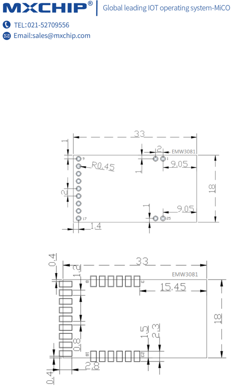
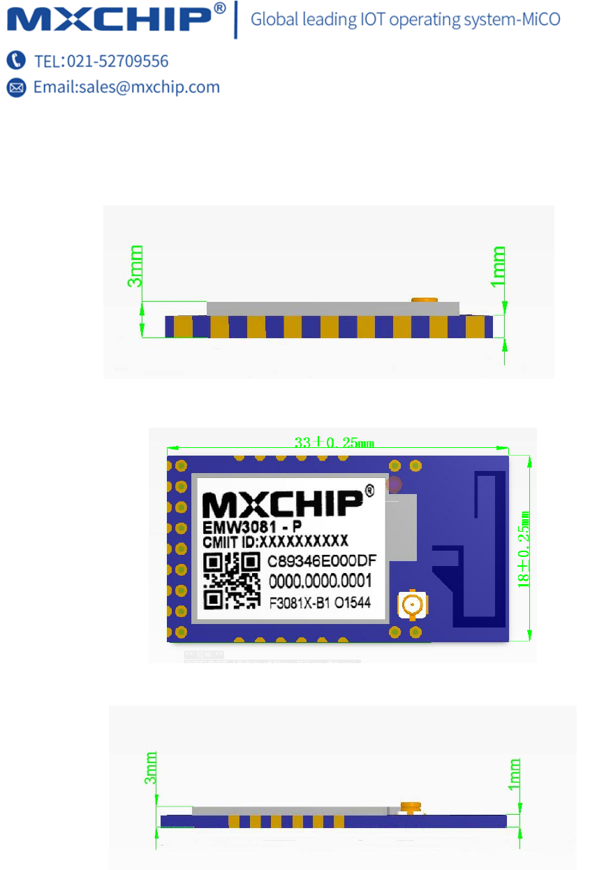
1.1. Pinouts
EMW3081 uses DIP packages and stamps hole packages interface design,DIP packages(figure
2)can effectively reduce the risk of quality of secondary patch;Stamp hole packages(figure 3)
facilitate customers to debug and easy installation, designed to provide customers diversity selection.
Windows and solder pads have the same size,recommended SMT stencil thickness is
0.12mm-0.14mm.
Figure2.DIPpackagedimension
Figure3.Stampholepackagesdimension
6
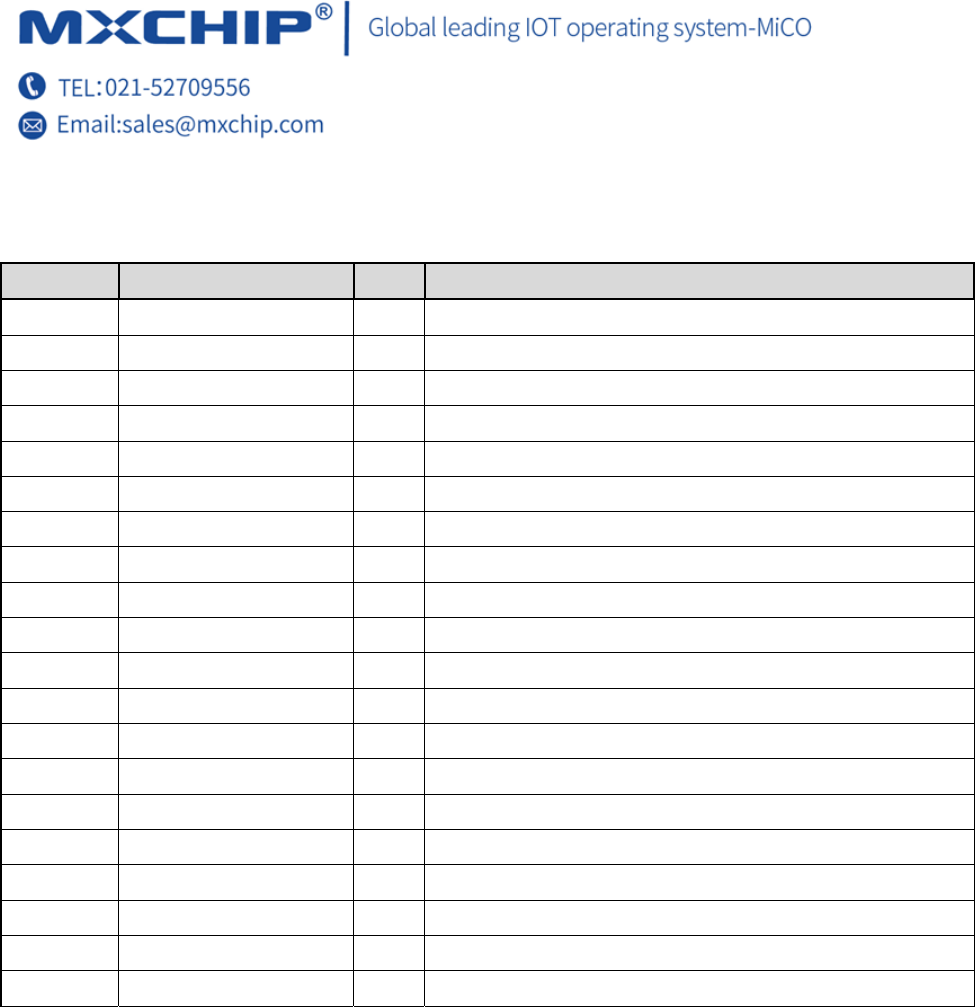
1.2. Pins Definition
Table1.EMW3081Pinsdefinition
Pin Number Name Type Function
1,3 PE4/SWCLK I/O SWCLK
2,4 PE3/SWDIO I/O SWDIO
5,6 NC NC
7 PA3/UART0_RTS I/O USER_UART_RTS
(either UART or IO)
8 PA5/UART0_CTS I/O USER_UART_CTS
(either UART or IO)
9 PA7/UART0_TXD I/O USER_UART_TX
(either UART or IO)
10 PA6/UART0_RXD I/O USER_UART_RX
(either UART or IO)
11 CHIP_EN I CHIP_EN
(Module enabled, active high)
12 PC0/SPI0_CS/PWM I/O SPI0_CS
(IO not available when used as SPI or PWM)
13 PC3/SPI0_MISO/PWM I/O SPI0_MISO
(O not available when used as SPI or PWM)
14 PC2/SPI0_MOSI/PWM I/O SPI0_MOSI
(O not available when used as SPI or PWM)
15 PC1/SPI0_CLK/PWM I/O SPI0_CLK
(O not available when used as SPI or PWM)
16 VDD S
VDD
17 GND S
GND
18 NC
NC
19 PC4/I2C1_SDA/BOOT I/O
BOOT
20 PC5/I2CI_SCL/STATUS I/O
STATUS
21,24 PB0/DEBUG_TXD I/O DEBUG_OUT
(either DEBUG or IO)
22,25 PB1/DEBUG_RXD I/O DEBUG_IN
(either DEBUG or IO)
23 PB_3/ELINK I/O ELINK
z S indicates power pin,I/O indicates GPIO;
z NC indicates not connect,Customers do not use this pin;
z I indicates Input;
z The bold italic indicates standard functions definition for this pin

7
8
2. Electrical Parameters
2.1 Operating Conditions
EMW3081 input voltage falls below the minimum rated voltage will cause instability. Must note
this point when designed power supply.
Table2.Inputvoltagerange
Symbol Description Condition
Detail
Min Typ Max Unit
VDD Power supply 3.0 3.3 3.6 V
Stresses above the absolute maximum ratings may cause permanent damage to the device.
These are stress ratings only and functional operation of the device at these conditions is not implied.
Exposure to maximum rating conditions for extended periods may affect device reliability.
Table3.Ratedvoltageparameters
Symbol Description Min Typ Unit
VDD The input voltage of Module power supply –0.3 3.6 V
VIN The pin’s input voltage of GPIO −0.3 3.6 V
2.2 Power Parameters
Table4.EMW3081powerparameters
Condition Current(3V3) Description
Deep sleep 16 uA Waked up by low power timer and GPIO
triggering
Sleep 19 mA Stay connected but no data transfer
Only CPU operation mode 33 mA CPU clock at 166MHZ, UART/SPI/I2C is
available, Wi-Fi is unavailable
11n RX mode 61 mA CPU clock at 166MHZ, UART/SPI/I2C is
available, Wi-Fi operates in 11n RX data
rece
p
tion mode
9
11n TX(when power
transmission is 13 dBm) 260mA CPU clock at 166MHZ, UART/SPI/I2C is
available, Wi-Fi operates in 11n TX data
transmission mode
Note: The test data at different firmware versions may be different.
2.3 Operating Environment
Table5.Temp eratu reandhumidityconditions
Symbol Name Range Unit
TSTG Storage temperature -40 to +85 ℃
TA Operate temperature -20 to +85 ℃
Humidity Noncondensing , relative humidity 95 %
2.4 ESD
Table6.ESDparameters
Symbol Ratings Conditions Class Max Unit
VESD(HBM)
Electrostatic discharge voltage
(human body model)
TA= +25 °C conforming
to JESD22-A114 2 2000
V
VESD(CDM)
Electrostatic discharge voltage
(charge device model)
TA = +25 °C conforming
to JESD22-C101 II 500

10
11
3. RF Parameters
3.1. General Specification
Table7.RFStandard
project Instructions
Operating Frequency 2.412~2.462GHz
Wi-Fi Standard IEEE802.11b/g/n
Date Transmission Rate
20MHz
11b:1,2,5.5,11Mbps
11g : 6,9,12,18,24,36,48,54Mbps
11n : MCS0~7, 72.2Mbps
(Channel 1~11)
40MHz 11n:MCS0~7, 150Mbps
(Channel 3~9)
Antenna type PCB antenna(default)
IPX external antenna (optional)
12
4. Antenna Information
4.1. Antenna type
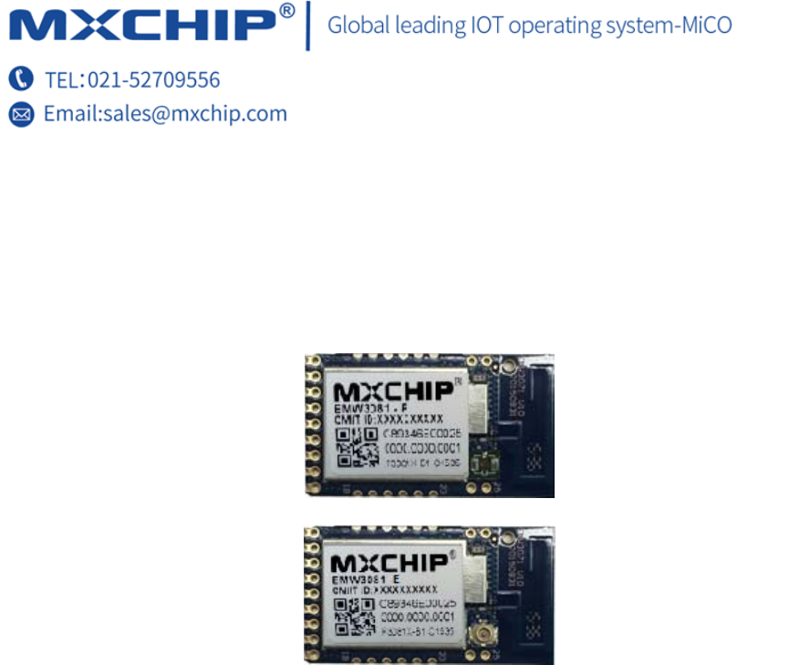
EMW3081 have two antenna types: PCB built-in antenna and external antenna, the models are
EMW3081-P and EMW3081-E.
Figure4.EWM3081‐P
Figure5.EMW3081‐E
4.2. PCB antenna design requirements
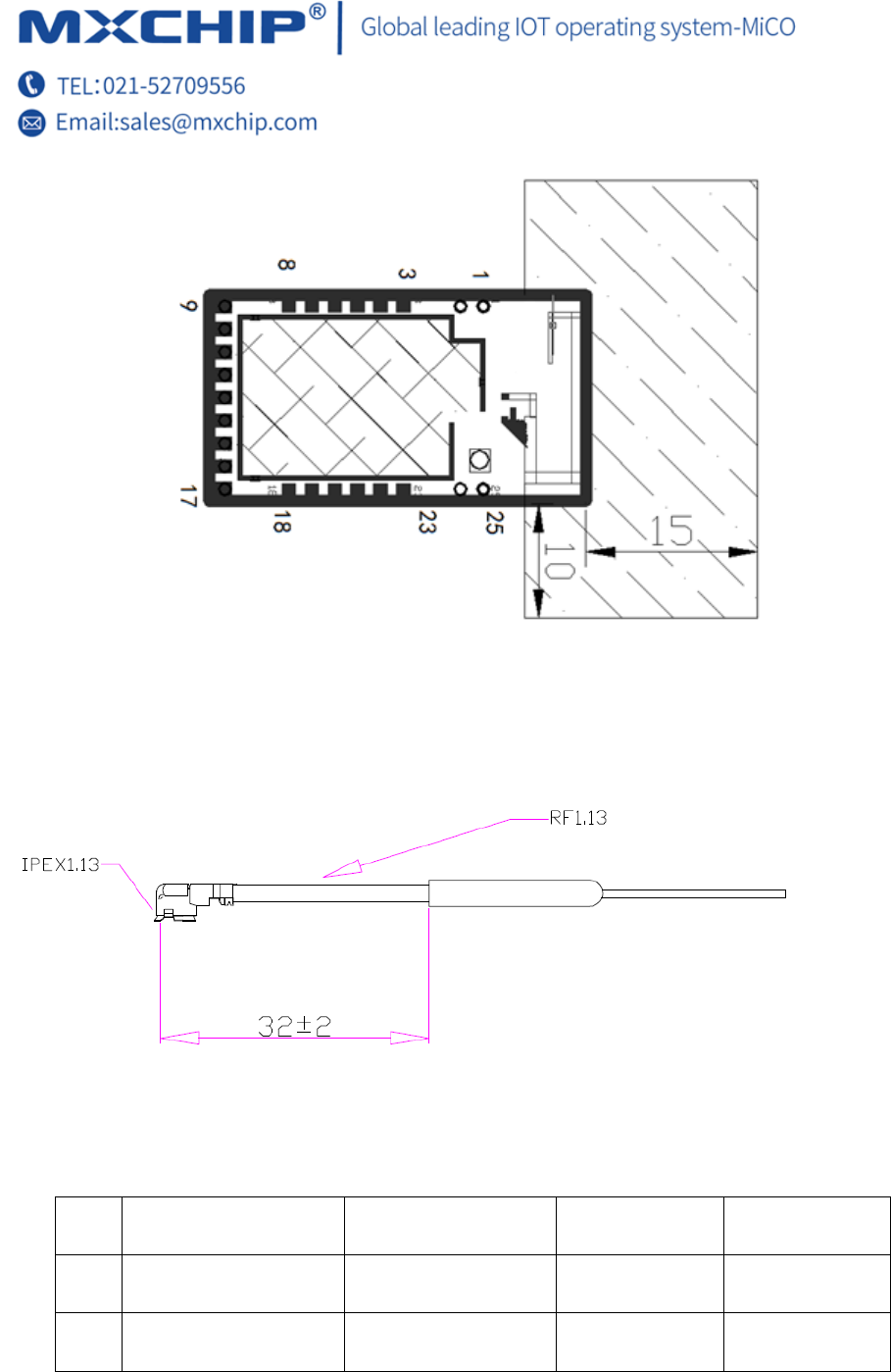
Components are strictly forbidden to place in the surrounding 15mm of PCB antenna area in module.
Such the shaded area need away from metal devices, sensors, interference sources and other
materials may cause signal interference。
13
Figure6.PCBantennaminimumclearancezone(Unit:mm)
4.3. Approved External Antenna Specification
Model Name:IPEX1.13-2.4G Brass Pipe Antenna-L32
Manufacture Name: Shenzhen Zhengda Letter Communications Equipment Co.,Ltd
NO. NAME DESCRIPTION QUANTITY PART NUMBER
1 Cable L =32±2mm 1 1301-0010
2 Brass Pipe 4.4*23mm 1 1113-0004
14
3 IPEX 20278-113R 1 1101-0001
Gain: <2.0dBi
Impedance: 50OHM
Frequency Range: 2400-2500MHz
VSWR <2.0
To meet requirements of design, External Antenna must satisfy parameters above.
15
4.4. U.F.L RF Connector
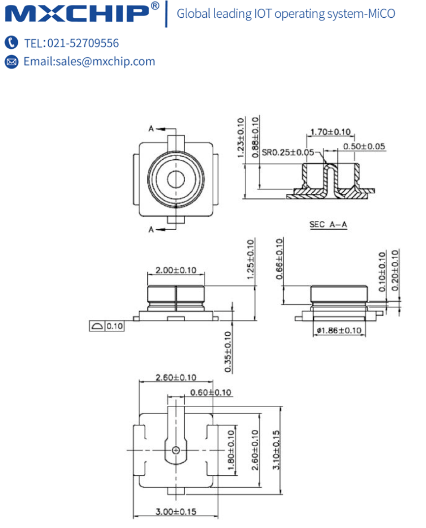
Figure7.Externalantennaconnectorsizediagram
16
5. The assembly information and manufacturing guidance
5.1. Mechanical dimensions
Figure8.SideView(Unit:mm)
Figure9.VerticalView(Unit:mm)
Figure10.LeftView(Unit:mm)

17
5.2. Use guidelines(Please read carefully)
z Stamps Wi-Fi modules from MXCHIP must be soldered with SMT machine. After unpacking
and burn the firmware patch must be completed within 24, or to re-vacuum packaging, Must be
baking before patching the modules
SMT need machine:
(1)Reflow soldering SMT machine
(2)The AOI detector
(3)6-8 mm diameter suction nozzle
baking need equipment:
(1)Cabinet baking box
(2)The antistatic, high temperature resistant tray
(3)The antistatic high temperature resistant gloves
z Storage conditions as follows:
(1)Moisture bag must be stored in a temperature < 30 ° C, humidity 85% RH of the
environment.
(2)Dry packing products, the guarantee period should be from 6 months from the date of
Packing seal.
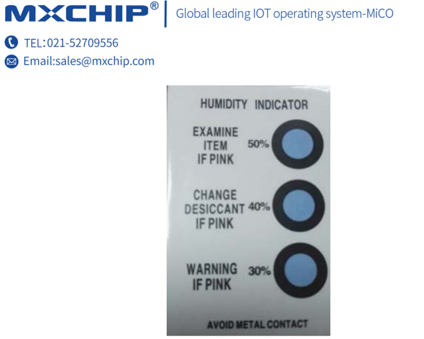
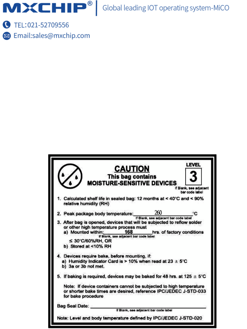
(3)Sealed packaging is equipped with humidity indicator card, as shown in Figure 11.
18
Table11.Temp eratu reandhumidityindicatorCARDS
z Humidity indicator CARDS and baking several ways as follow:
When opened, if the temperature and humidity indicator CARDS read 30%, 40%, 50%, three
colors are blue, to continue to bake for 2 hours for module;
When opened, if the humidity indicator CARDS read 30% color ring into pink, need to continue
to bake module 4 hours;
When opened, if the humidity indicator CARDS read into 30%, 40%, color ring into pink, need to
continue to bake for 6 hours module;
When opened, if the humidity indicator CARDS read into 30%, 40%, 50% are pink color ring,
need to continue to bake for 12 hours module;
When opened, if the humidity indicator CARDS read into 10%, 20%, 30% ,40%are pink

19
color ring, need to continue to bake for 14 hours module;
z Baking parameters are as follows:
Baking temperature: 125 ℃ + / - 5 ℃;
Set the alarm temperature as 130 ℃;
Under the condition of natural cooling < 36 ℃, SMT placement can be made;
Dry times: 1 times;
z If opened the time more than 3 months, please ban the use of SMT process welding this batch
module, zedoary because PCB process, more than 3 months bonding pad oxidation, SMT is
likely to cause virtual welding, welding, the resulting problems we do not assume
corresponding responsibility.
z Please to ESD(static discharge,static electricity discharge) protection module before SMT;
z Please according to the SMT reflow soldering curve, peak temperature 245 ℃, reflow soldering
temperature curve as shown in figure 11,section 5.5.
z For the first time in order to ensure the qualified rate of reflow soldering, first SMT please
extraction 10% product to visual analysis, AOI inspection, to ensure that the furnace
temperature control, device adsorption method, the rationality of the put way; Suggestions:
when batch production per hour 5-10 pieces of visual analysis, AOI test.
5.3. The matters needing attention
z In the entire production, Each station of the operator must wear anti-static gloves;
z When baking, no more than baking time;
z When roasting, it is forbidden to join explosive, flammable, corrosive substances;
z When baking, high temperature module application tray in the oven, keep the air circulation
between each module, at the same time avoid direct contact with the oven wall module;
z Baking, please will bake the door is closed, the guarantee baking box sealing, prevent leakage,
temperature influence the baking effect;
20
z Don't open the door, as far as possible when baking box running if must open, shortening the
time of can open the door as far as possible;
z After baking, must be natural cooling modules to < 36 ℃ before wear anti-static gloves out, so
as not to burn.
z Operation, forbidden module bottom touch water or dirt;
z Temperature and humidity control level for Level3, storage and baking conditions based on
IPC/JEDEC J - STD - 020.
5.4. MSL/Storage Condition
Figure12.StorageCondition
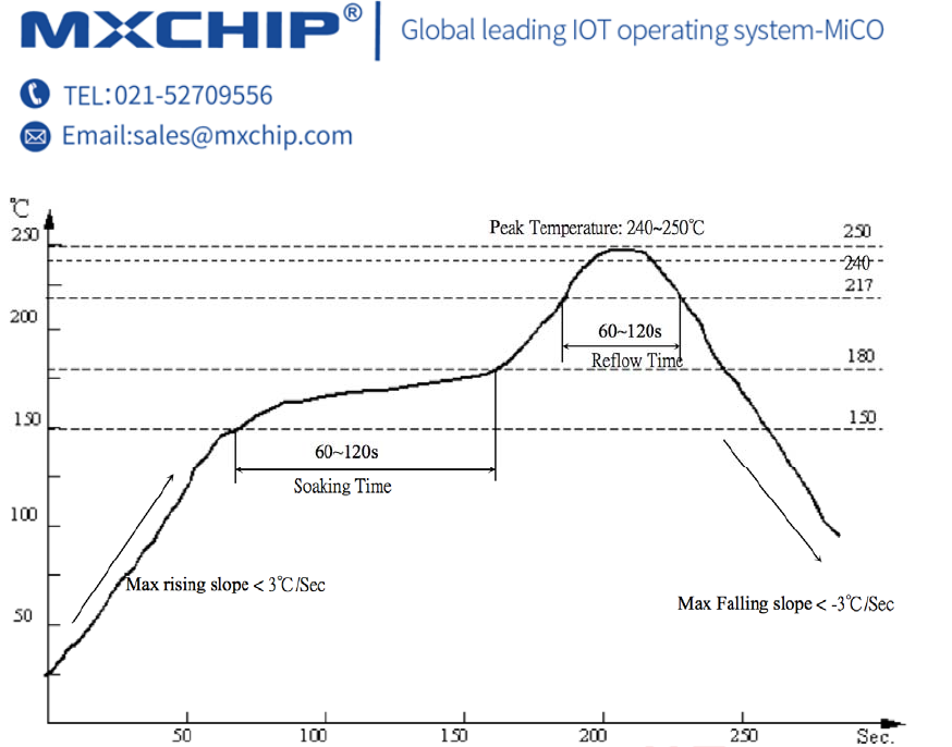
5.5. Recommended Reflow Profile
Reflow times<= 2times (Max.)
21
Figure13.Temp eratu reCurve
22
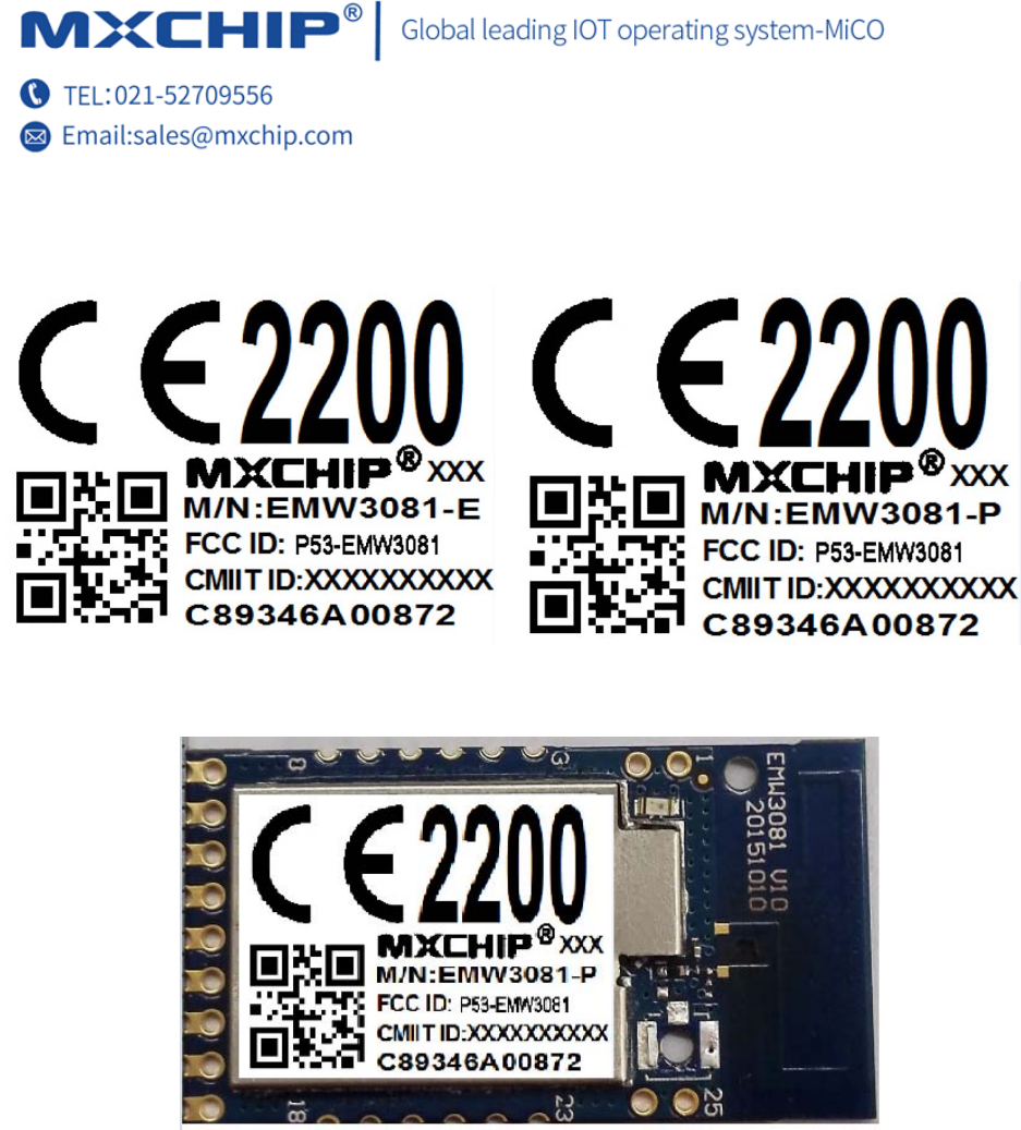
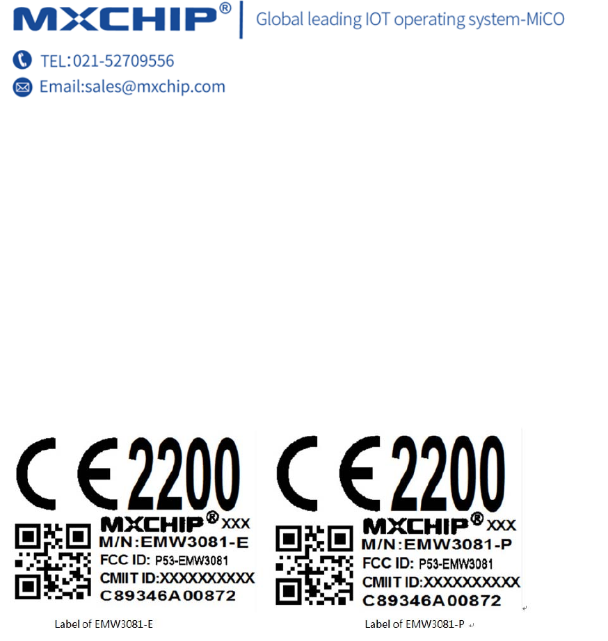
6. Label
Label of EMW3081-E Label of EMW3081-P
Label of Location

23
7. Firmware encrypt
Firmware version : 0000.0000.AL10
In order to make sure the firmware could not be modified after programming in the module by
unauthorized party, firmware must be encrypted with the bootloader drivers and the chip ID
MXCHIP offered.
Bootloaderdriver is used to drive the device in the module and integrated with one AES
encryption way. The application part of the firmware must be combined with the bootloader
driver to generate one MVA/bin file after adding the chip ID details which can be used to identify
MXCHIP module. Check the official website for more information.
Note:
Unauthorized party is forbidden from modification.
Everyone cannot change new firmware by anyway , otherwise it will cause bad work.

24
8. FCC Statement
This device complies with Part 15 of the FCC Rules. Operation is subject to the following two
conditions:
(1) this device may not cause harmful interference, and
(2) this device must accept any interference received, including interference that may cause
undesired operation.
NOTE: The manufacturer is not responsible for any radio or TV interference caused by
unauthorized modifications to this equipment. Such modifications could void the user's authority
to operate the equipment.
NOTE: This equipment has been tested and found to comply with the limits for a Class B digital
device, pursuant to part 15 of the FCC Rules. These limits are designed to provide reasonable
protection against harmful interference in a residential installation. This equipment generates
uses and can radiate radio frequency energy and, if not installed and used in accordance with the
instructions, may cause harmful interference to radio communications. However, there is no
guarantee that interference will not occur in a particular installation. If this equipment does cause
harmful interference to radio or television reception, which can be determined by turning the
equipment off and on, the user is encouraged to try to correct the interference by one or more of
the following measures:
-Reorient or relocate the receiving antenna.
-Increase the separation between the equipment and receiver.
-Connect the equipment into an outlet on a circuit different from that to which the receiver is
connected.
-Consult the dealer or an experienced radio/TV technician for help.
RF Exposure Information
This equipment complies with FCC radiation exposure limits set forth for an uncontrolled
environment. This equipment should be installed and operated with minimum distance 20cm
25
between the radiator & your body.
This module is only used into fixed host applications.
The module is only for integration in fixed applications.
Label Information to the End User by the OEM or Integrators
This Module used affixed label with FCC ID: P53-EMW3081. If the FCC ID of this module is not visible
when it is installed inside another device, then the outside of the device into which the module is
installed must be label with "Contains FCC ID: P53-EMW3081".
The labels above must be included in the application for equipment Authorization;
This module complies with Part 15 of the FCC rules, but the usage of module by integrator (OEM) is
subject to and fully informed of the following conditions:
Integrator (OEM) is Responsible for ensuring host complying with the according FCC rules, when
module collocates with other radiators operating individually or simultaneously. This includes
compliance for the summation of all emissions from all output occupying the same or overlapping
frequency ranges, as defined by the applicable FCC rules.
Necessary actions by integrator (OEM) on final host devices with compliance and authorization:
The integrator shall not use any other antennas except the approved one or same type with same in
and out of band characteristics, otherwise additional approvals are necessary.

26
Changes or modification unapproved on module may break compliance, otherwise additional
approvals are performed.
Changes or modifications not expressly approved by the party responsible for compliance could void
the user's authority to operate the equipment.
The devices must be installed and used in strict accordance with the manufacturer's instructions as
described in the user documentation that comes with the product.

27
9. Sales Information and Technical Support
If you need to get the latest information on this product or our buy this product,please call us during
the working hours.
Office hours:
From Monday to Friday, morning 9:00~12:00, afternoon 13:00~18:00
Telephone: +86-21-52655026
Contact address: 9F, 5 Building, No.2145 Jinshajiang Road, Shanghai, China
Postcode : 200333
Email: sales@mxchip.com