MXCHIP Information Technology EMW3162 Embedded WiFi module User Manual
Shanghai MXCHIP Information Technology Co.,Ltd. Embedded WiFi module
User Manual
1
Warning statement
FCC STATEMENT
1. This device complies with Part 15 of the FCC Rules. Operation is subject to the following
two conditions:
(1) This device may not cause harmful interference.
(2) This device must accept any interference received, including interference that may
cause undesired operation.
2. Changes or modifications not expressly approved by the party responsible for
compliance could void the user's authority to operate the equipment.
NOTE: This equipment has been tested and found to comply with the limits for a Class B
digital device, pursuant to Part 15 of the FCC Rules. These limits are designed to provide
reasonable protection against harmful interference in a residential installation.
This equipment generates uses and can radiate radio frequency energy and, if not installed
and used in accordance with the instructions, may cause harmful interference to radio
communications. However, there is no guarantee that interference will not occur in a
particular installation. If this equipment does cause harmful interference to radio or
television reception, which can be determined by turning the equipment off and on, the
user is encouraged to try to correct the interference by one or more of the following
measures:
Reorient or relocate the receiving antenna.
Increase the separation between the equipment and receiver.
Connect the equipment into an outlet on a circuit different from that to which the
receiver is connected.
Consult the dealer or an experienced radio/TV technician for help.
FCC Radiation Exposure Statement
This equipment complies with FCC radiation exposure limits set forth for an uncontrolled
environment. This equipment should be installed and operated with minimum distance
20cm between the radiator & your body.
The EMW3162 module is designed to comply with the FCC statement. FCC ID is
P53-EMW3162. The host system using EMW3162, should have label indicated FCC ID
P53-EMW3162.

2
User Manual
Embedded M2M Module with 802.11b/g/n 1T1R WiFi
(Project Name) Embedded M2M Module with Broadcom
802.11bgn(1x1) WiFi single chip
(Foxconn Part No.) T77H497.00
(Customer Part No.) EMW3162
3
Content
1. INTRODUCTION ........................................................................... 4
1.1 RF MODULE OVERVIEW ..................................................................... 4
1.2 SPECIFICATION REFERENCE .................................................................. 4
1.3 SYSTEM FUNCTIONS ........................................................................ 5
2. MECHANICAL SPECIFICATION ............................................................. 6
2.1 MECHANICAL DRAWING ...................................................................... 6
2.2 44PIN QFN PIN DEFINITION .................................................................. 7
3. ELECTRICAL SPECIFICATION .............................................................. 8
3.1 802.11B MODE ............................................................................ 8
3.2 802.11G MODE ............................................................................ 9
3.3 802.11N HT20 MODE ...................................................................... 10
4
1. Introduction
Project Name: Embedded M2M Module with Broadcom 802.11bgn (1x1) WiFi.
Project Number: T77H497.00.
This documentation describes the engineering requirements specification of WiFi module
with T77H497.00. It is a confidential document of Foxconn.
1.1 RF module Overview
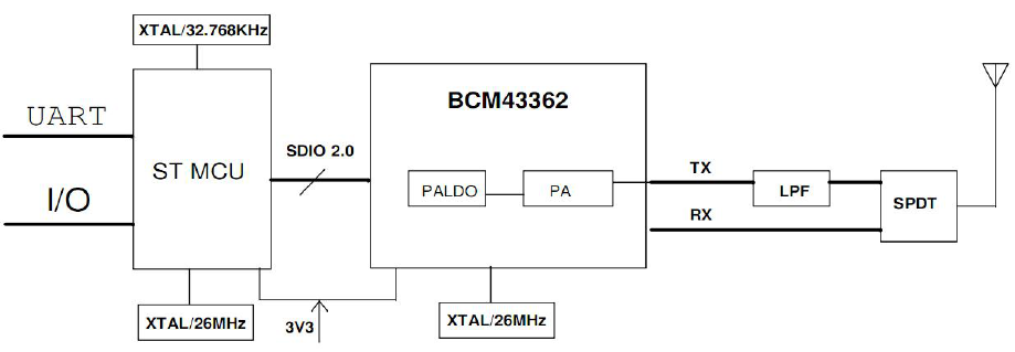
This M2M (Machine to Machine) module integrates 32 bit MCU and Broadcom WiFi. It
provides wireless modem functionality utilizing direct sequence spread spectrum and
OFDM/CCK technology. It operates in 2.4GHz ISM band, compatible with the IEEE
802.11b/g/n standard. It can implement the wireless network function on the embedded
devices easily and improve the product’s competitiveness. It supports TCP/IP protocol and
all of the Wi-Fi security. This module has implemented some efficient mechanisms in its
software and hardware to maximize the performance.
The functional block diagram is shown in Figure .1.
Figure 1 Module Block Diagram
1.2 Specification reference
This specification is based on additional references listed below.
IEEE Std. 802.11b
IEEE Std. 802.11g
IEEE Std. 802.11n
5
1.3 System Functions
Table1: General Specification as below:
Main Chipset 32 bit MCU and Broadcom WiFi single chip
Operating Frequency 2412MHz~2462MHz
WiFi Standard 802.11b/g/n(1x1)
Modulation 11b: DBPSK, DQPSK, CCK and DSSS
11g: BPSK, QPSK, 16QAM, 64QAM and OFDM
11n: MCS0~7 OFDM
PHY Data rates 11b: 1, 2, 5.5 and 11Mbps
11g: 6, 9, 12, 18, 24, 36, 48 and 54 Mbps
11n(HT20): MCS0~7, up to 150Mbps
Form factor 44pin QFN design
Host Interface SDIO 2.0
PCB Stack 4-layers single side design
PCBA Dimension Typical, 38.60mm(W)*23.62mm(L)*3.30mm(T)
Antenna Type One printed antenna on board
One U.F.L connector for external antenna
Operation Temperature -30℃ to +80℃
Storage Temperature -40℃ to +85℃
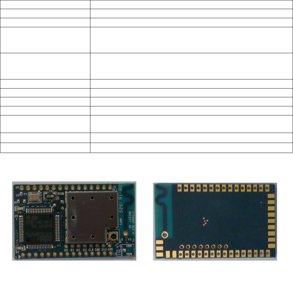
Sample picture is as below.
BOTTOM
TOP
6
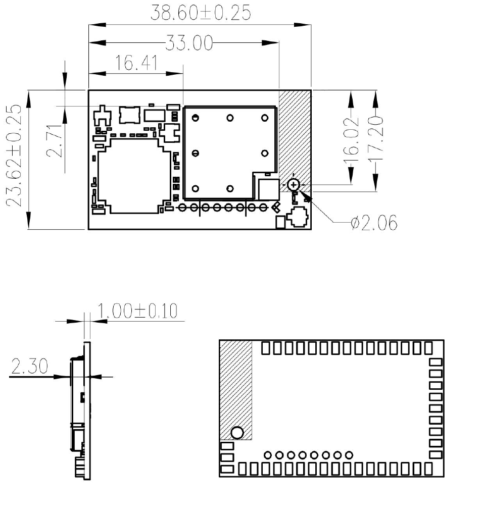
2. Mechanical Specification
2.1 Mechanical Drawing
Typical Dimension (W x L x T ): 38.60x23.62x3.30 mm
.
TOP VIEW
BOTTOM VIEW SIDE VIEW
Unit: mm
31
39
1 1540
44
16 30

7
2.2 44pin QFN Pin definition
The pin definition is as below, and its pin number refers to item 2.1.
Pin # Name Pin # Name
1 I2C_SCL 21 nCTS_DM
2 I2C_SDA 22 TXD
3 JTMSSWDIO 23 RXD
4 I2S_MCK 24 VCC3V3
5 PA3_RX2-TCP 26 32K_SLPCLK_OUT
6 SPI-NSS_I2S-WS 27 BOOT0
7 JTDO_SPI-CLK_I2S-CK 28 JTCKSWCLK
8 NJTRST_SPI-MISO_I2Sext_SD 29 WAKE_UP
9 SPI-MOSI_I2S-SD 30 status
10 SPI_INT 31 GPIO_PA5
11 Readyness 32 GPIO_PA6
12 GPIO_PC2 33 GPIO_PA7
13 GPIO_PB14 34 GPIO_PB15
14 GPIO_PC6 35 GPIO_PC3
16 nRF_LED 36 GPIO_PC4
17 nRESET 37 GPIO_PC0
18 JTDI_DSR 38 PA2_TX2
19 DATA_RDY 15,25,39~44 GND
20 nRTS_DP

8
3. Electrical Specification
3.1 802.11b Mode
Items Contents
Standard IEEE802.11b
Modulation Type DSSS / CCK
Frequency range 2412MHz~2462MHz
Channel CH1 to CH11
Data rate 1, 2, 5.5, 11Mbps
TX Characteristics Min. Typ. Max. Unit
1. Transmitter Output Power
1) 11b Target Power 15 16.5 18 dBm
2. Spectrum Mask @ target power
1) fc +/-11MHz to +/-22MHz - - -30 dBr
2) fc > +/-22MHz - - -50 dBr
3. Frequency Error -25 - +25 ppm
4 Constellation Error( peak EVM)@ target power
1) 1~11Mbps - - 35%
RX Characteristics Min. Typ. Max. Unit
5 Minimum Input Level Sensitivity
1) 1Mbps (FER≦8%) - -
-83 dBm
2) 2Mbps (FER≦8%) - -
-80 dBm
3) 5.5Mbps (FER≦8%) - -
-79 dBm
4) 11Mbps (FER≦8%) - -
-76 dBm
6 Maximum Input Level (FER≦8%) -10 - - dBm

9
3.2 802.11g Mode
Items Contents
Standard IEEE802.11g
Modulation Type OFDM
Frequency range 2412MHz~2462MHz
Channel CH1 to CH11
Data rate 6, 9, 12, 18, 24, 36, 48, 54Mbps
TX Characteristics Min. Typ. Max. Unit
1. Transmitter Output Power
1) 11g Target Power 11.5 13 14.5 dBm
2. Spectrum Mask @ target power
1) at fc +/- 11MHz - - -20 dBr
2) at fc +/- 20MHz - - -28 dBr
3) at fc > +/-30MHz - - -40 dBr
3 Constellation Error(EVM)@ target power
1) 6Mbps - - -5 dB
2) 9Mbps - - -8 dB
3) 12Mbps - - -10 dB
4) 18Mbps - - -13 dB
5) 24Mbps - - -16 dB
6) 36Mbps - - -19 dB
7) 48Mbps - - -22 dB
8) 54Mbps - - -25 dB
4 Frequency Error -25 - +25 ppm
RX Characteristics Min. Typ. Max. Unit
5 Minimum Input Level Sensitivity
1) 6Mbps (PER ≦ 10%) - - -82 dBm
2) 9Mbps (PER ≦ 10%) - --87 dBm
3) 12Mbps (PER ≦ 10%) - - -79 dBm
4) 18Mbps (PER ≦ 10%) - - -77 dBm
5) 24Mbps (PER ≦ 10%) - --74 dBm
6) 36Mbps (PER ≦ 10%) - - -70 dBm
7) 48Mbps (PER ≦ 10%) - - -66 dBm
8) 54Mbps (PER ≦ 10%) - - -65 dBm
6 Maximum Input Level (PER ≦ 10%) -20 - - dBm

10
3.3 802.11n HT20 Mode
Items Contents
Standard IEEE802.11n HT20 @ 2.4GHz
Modulation type MIMO-OFDM
Channel CH1 to CH11
Data rate (MCS index) MCS0/1/2/3/4/5/6/7
TX Characteristics Min. Typ. Max. Unit
1. Transmitter Output Power
1) 11n HT20 Target Power
10.5 12 13.5 dBm
2. Spectrum Mask @ target power
1) at fc +/- 11MHz ---20dB
r
2) at fc +/- 20MHz - - -28 dBr
3) at fc > +/-30MHz - - -45 dBr
3. Constellation Error(EVM)@ target power
1) MCS0 - -
-5 dB
2) MCS1 - -
-10 dB
3) MCS2 --
-13 dB
4) MCS3 - -
-16 dB
5) MCS4 - -
-19 dB
6) MCS5 --
-22 dB
7) MCS6 - -
-25 dB
8) MCS7 - -
-27 dB
4. Frequency Error -25 - +25 ppm
RX Characteristics Min. Typ. Max. Unit
5. Minimum Input Level Sensitivity
1) MCS0 (PER ≦ 10%) - - -82 dBm
2) MCS1 (PER ≦ 10%) - - -79 dBm
3) MCS2 (PER ≦ 10%) - - -77 dBm
4) MCS3 (PER ≦ 10%) - - -74 dBm
5) MCS4 (PER ≦ 10%) - - -70 dBm
6) MCS5 (PER ≦ 10%) - - -66 dBm
7) MCS6 (PER ≦ 10%) - - -65 dBm
8) MCS7 (PER ≦ 10%) - - -64 dBm
6. Maximum Input Level (PER ≦ 10%) -20 - - dBm