MXCHIP Information Technology EMW3166 Embedded WiFi module User Manual xxxDataSheet
Shanghai MXCHIP Information Technology Co.,Ltd. Embedded WiFi module xxxDataSheet
User Manual
Shanghai MXCHIP Information Technology Co., Ltd.
Address:Floor 9, Building 5, No. 2145, Putuo District, Shanghai (200333) Telephone:021-52709556 Website:http://mxchip.com/
Track Number: AN00048EN
MXCHIP Co., Ltd
Version: 0.3
11.17.2016
Category: Application Note
Open
EMW3166 _Guide For User Design
Abstract
This note lists the matters need attention in each stage of designing and manufacturing while using MXCHIP module.
In order to achieve rapid mass production, application designers need learn this note first. Consider and avoid all
possible problems which may happen during designing, manufacturing, firmware programming and testing ahead of
time.
More Help
Please login the website: http://mxchip.com/ to get Mxchip's latest product information.
You can also login MiCO Developer Forum: http://mico.io/ to get more recent development information about
MiCO.
You can also login MiCO Developer Forum: http://easylink.io/ to get more recent development information about
FogCloud.
Application Note [Page 1]
EMW3166_Guide For User Design
Version Record
Date
Version
Update content
9-23-2016
V0.1
Initial version.
9-23-2016
V0.2
Add reference circuit
11-17-2016
V0.3
Update FW download and test method

Application Note [Page 2]
EMW3166_Guide For User Design
Catalog
EMW3166 _Guide For User Design .................................................................................................................................. 1
Version Record .................................................................................................................................................................... 1
1. Introduction ................................................................................................................................................................. 4
2. Hardware design attention ......................................................................................................................................... 6
Mechanical dimensions .................................................................................................................................... 6 2.1
Recommended package design ........................................................................................................................ 6 2.2
DC power design ............................................................................................................................................. 7 2.3
Recommended circuit design ........................................................................................................................... 7 2.4
RF design ......................................................................................................................................................... 9 2.5
2.5.1 PCB antenna design ............................................................................................................................. 9
2.5.2 T U.F.L RF Connector ....................................................................................................................... 10
ESD design .................................................................................................................................................... 11 2.6
3. Firmware programming and warehousing detection method ............................................................................... 12
Receiving Inspection Device List .................................................................................................................. 12 3.1
Collection ....................................................................................................................................................... 12 3.2
Warehousing detection ................................................................................................................................... 12 3.3
3.3.1 Software setting ................................................................................................................................. 12
3.3.2 Module testing ................................................................................................................................... 13
3.3.3 Testing result ..................................................................................................................................... 13
Statements ...................................................................................................................................................... 14 3.4
4. SMT matters .............................................................................................................................................................. 15
Note for stencil aperture ................................................................................................................................. 15 4.1
Recommended reflow profile......................................................................................................................... 15 4.2
5. Mass production testing and firmware upgrading ................................................................................................. 17
Mass production test ...................................................................................................................................... 17 5.1
5.1.1 EMSP command way ........................................................................................................................ 17
5.1.2 Limited development firmware ......................................................................................................... 17
5.1.3 Full development firmware ............................................................................................................... 17
Upgrading ...................................................................................................................................................... 17 5.2
6. Firmware encrypt ..................................................................................................................................................... 18
7. Sales and technical support information ................................................................................................................ 19

Application Note [Page 3]
EMW3166_Guide For User Design
Picture Catalog
Figure 1 EMW3166 top view .............................................................................................................................. 4
Figure 2 EMW3166 Hardware block ................................................................................................................... 5
Figure 3 Vertical view .......................................................................................................................................... 6
Figure 4 side view ................................................................................................................................................ 6
Figure 5 Recommended Package for SMT .......................................................................................................... 7
Figure 6 Recommended Circuit Design ............................................................................................................... 8
Figure 7 Minimum Size of Keep-out Zone Around Antenna ............................................................................... 9
Figure 8 Module Position Recommended on Mother Board ............................................................................. 10
Figure 9 U.F.L Connector Size ........................................................................................................................... 11
Figure 10 Development Board Switch Settings ................................................................................................. 12
Figure 11 Hyper Terminal Setting Connection .................................................................................................. 13
Figure 12 Testing Results .................................................................................................................................. 14
Figure 13 Recommended Stencil Aperture ........................................................................................................ 15
Figure 14 Reflow soldering temperature curve ................................................................................................. 16
Table Catalog
Table 1 Warehousing Detection Equipment List ............................................................................................... 12
Application Note [Page 4]
EMW3166_Guide For User Design
1. Introduction
This note lists the matters need attention in each stage of designing and manufacturing while using MXCHIP module.
In order to achieve rapid mass production, application designers need learn this note first. Consider and avoid all
possible problems which may happen during designing, manufacturing, firmware programming and testing ahead of
time.
Applicative module type:
EMW3166 series
To note stage:
Hardware designing
Firmware programming
Production SMT
OTA upgrading
Basic features of module:
Globally unique MAC ID for each module
Two antenna designing types:
PCB printed antenna and external one using U.F.L RF connector
Peak current 320mA @ 3.3V
In-built production test mode
In-built OTA mode
Reflow soldering when SMT
EMW3166 top view:
Figure 1 EMW3166 top view
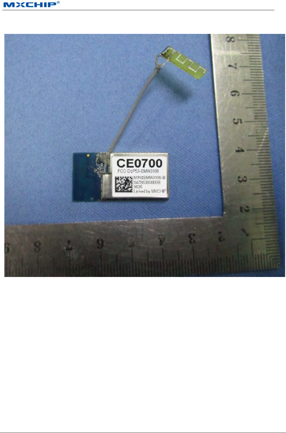
Figure 1 EMW3166 top view
EMW3166_Guide For User Design
Application Note [Page 4]
Application Note [Page 5]
EMW3166_Guide For User Design
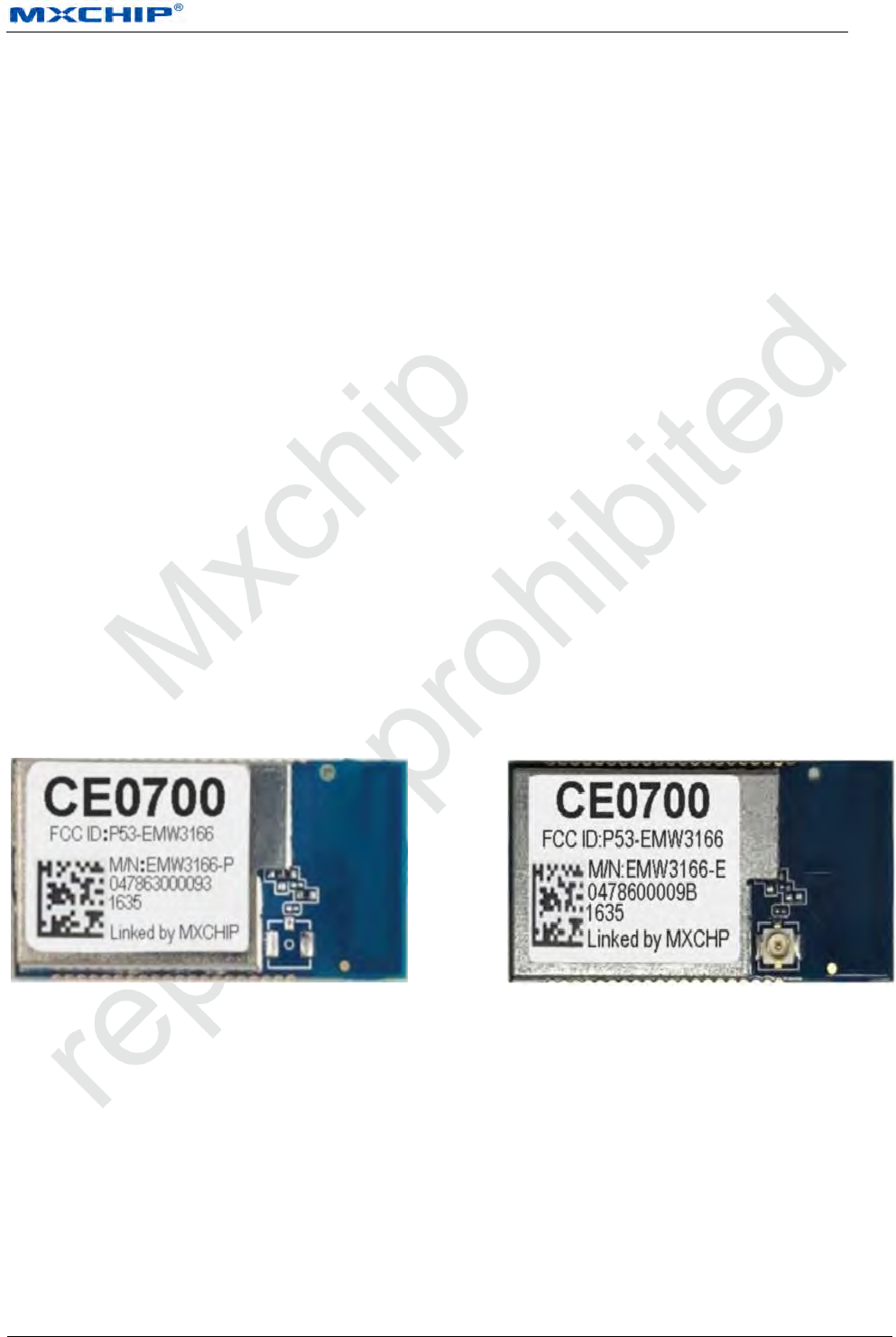
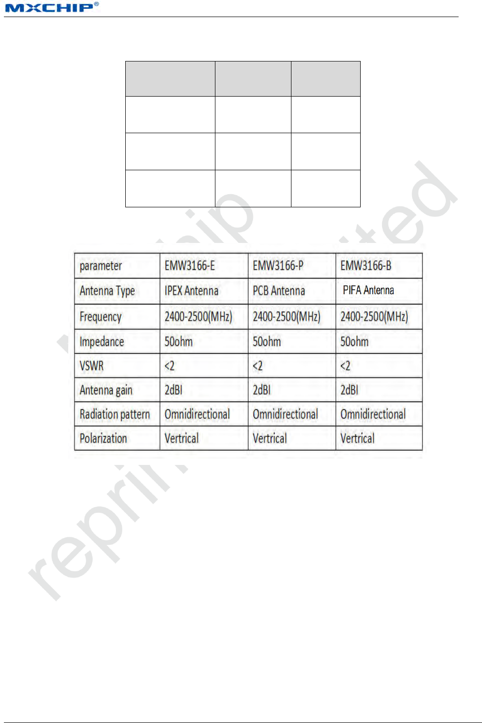
EMW3166 model list:
Module model
Antenna type
Description
EMW3166-P
PCB printed
Antenna
Default
EMW3166-E
External antenna
to IPX
Optional
EMW3166-B
PIFA antenna
Optional
EMW3166 Wi-Fi Module Hardware Block
Network
Processor
ADC
Flash
1M bytes
WLAN
Subsystem
2.4GHz radio
U.F.L connector
On-board
PCB Ant
Flash 2M
bytes
Power
Mangement
3.3V Input
26MHz
OSC
26MHz
OSC
SRAM
256K bytes
32.768KHz
OSC
Timer/PWM
UART
I2C
GPIO
SPI
SDIO
SPI
802.11b/g/n
MAC/Baseband/
radio
100MHz
Cortex-M4 MCU
Antenna Type:
[Page 6]
EMW3166
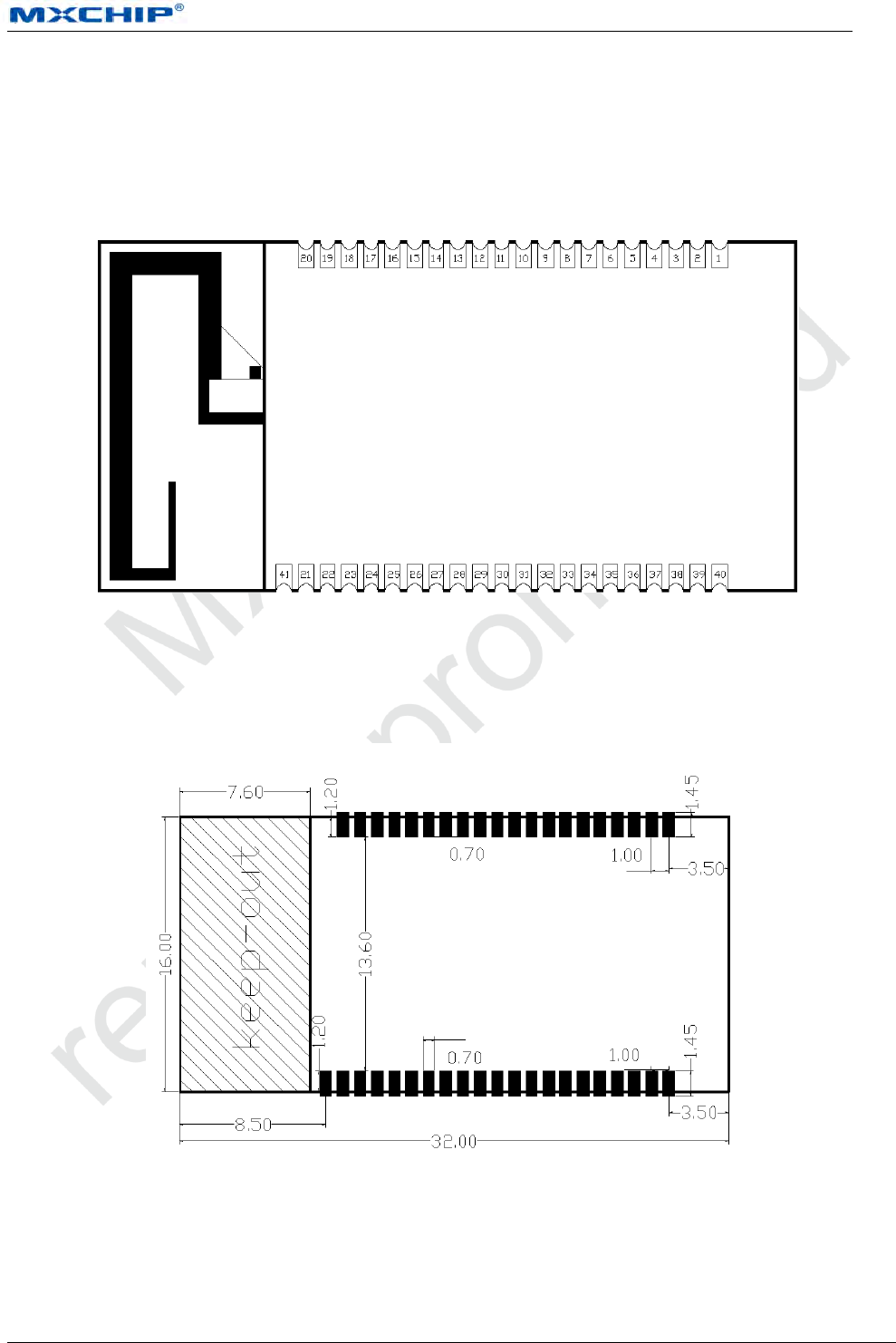
Pin Designation 1.2
EMW3166 owns two groups of pins (1X20 + 1X21). The lead pitch is 1mm.
EMW3166 has half-hole footprint fit for hand-soldering
EMW3166 pinouts:
Figure 5 Half-hole package dimension
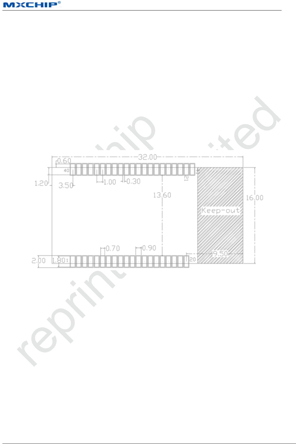
Recommended Footprint Design 1.3
Recommended footprint (Unit: mm):
Figure 6 Recommended Footprint
Pin Arrangement 1.4
The general pin description:
[Page 7]
EMW3166
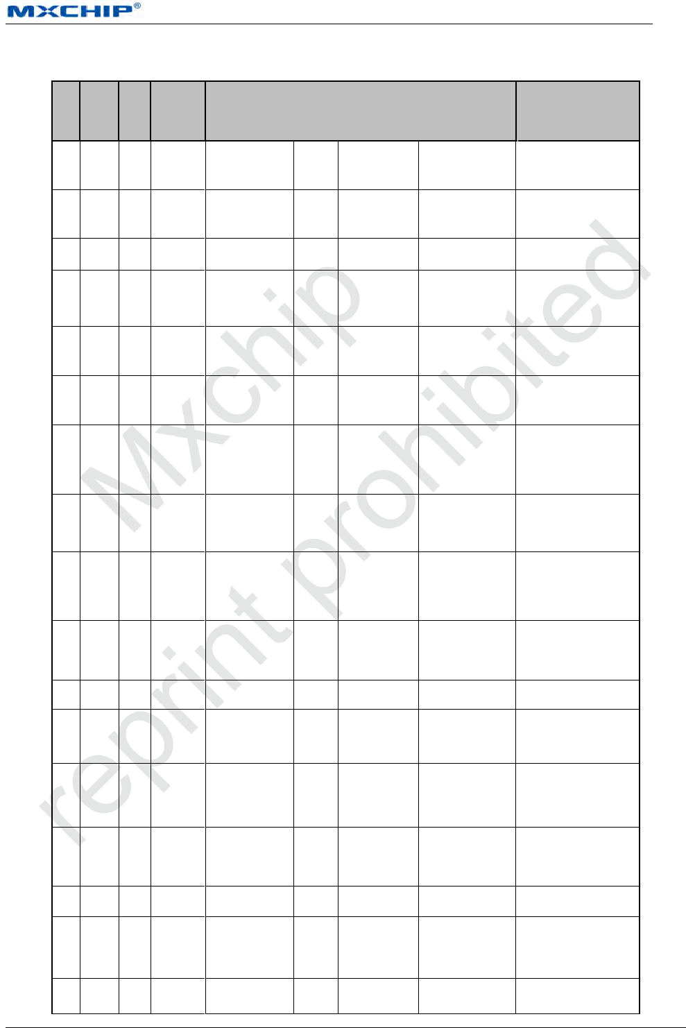
Table 1 EMW3166 pin arrangement
Pins
Name
Type
I/O level
Functions
Note
1
-
-
-
NC
2
PB2
I/O
FT
GPIO
BOOT1
√
3
-
-
-
NC
4
PB15
I/O
FT
SPI2_MOSI
GPIO
TIM12_CH2
I2S2_SD
√
5
PB12
I/O
FT
SPI2_NSS
GPIO
CAN2_RX
I2S2_WS
√
6
PB13
I/O
FT
SPI2_SCK GPIO CAN2_TX
I2S2_CK
√
7
PB14
I/O
FT
SPI2_MISO GPIO TIM12_CH1
√
8
PC6
I/O
FT
UART6_TXD GPIO TIM3_CH1
I2S2_MCK
×DEBUG_OUT
9
PA15
I/O
FT
GPIO
JTDI
TIM2_CH1
USART1_TXD
×(EasyLink)
10
VBAT
S
-
VBAT
×
11
-
-
-
NC
12
PC7
I/O
FT
UART6_RXD
GPIO
TIM3_CH2
I2S2_CK
×DEBUG_IN
13
NRST
I/O
FT
RESET
×
14
PC0
I
TC
GPIO
WAKEUP
√
15
-
-
-
NC
16
PC13
I/O
FT
GPIO
√
17
PB8
I/O
FT
I2C1_SCL
GPIO
TIM4_CH3
CAN1_RX
√
[Page 8]
EMW3166
Pins
Name
Type
I/O level
Functions
Note
18
PB9
I/O
FT
I2C1_SDA
GPIO
TIM4_CH4
CAN1_TX
√
19
PB10
I/O
FT
GPIO
TIM2_CH3
I2S2_CK
√
20
GND
S
-
GND
×
21
GND
S
-
GND
×
22
-
-
-
NC
23
-
-
-
NC
24
-
-
-
NC
25
PA14
I/O
FT
SWCLK
×
26
PA13
I/O
FT
SWDIO
×
27
PB3
I/O
FT
GPIO TIM2_CH2
USART1_RXD
√
28
-
-
-
NC
29
PB7
I/O
FT
UART1_RXD
GPIO TIM4_CH2
I2C1_SDA
√USER_UART_RX
30
PB6
I/O
FT
UART1_TXD
GPIO
TIM4_CH1
I2C1_SCL
√USER_UART_TX
31
PB4
I/O
FT
GPIO
JTRST
TIM3_CH1
√
32
-
-
-
NC
33
PA10
I/O
FT
USB_ID
GPIO
TIM1_CH3
√
34
PA5
I/O
TC
GPIO
ADC1_5
√
35
PA11
I/O
FT
USB_DM
GPIO
TIM1_CH4
UART1_CTS
√
36
PA12
I/O
FT
USB_DP
GPIO
TIM1_ETR
UART1_RTS
×(BOOT)
[Page 9]
EMW3166
Pins
Name
Type
I/O level
Functions
Note
37
PB0
I/O
FT
GPIO
ADC1_8
×(STATUS)
38
PA4
I/O
TC
GPIO
ADC1_4
√
39
VDD
S
-
3.3V
×
40
VDD
S
-
3.3V
×
41
ANT
-
-
ANT
×
Notes:
1. PIN10, PIN39, PIN40 need connect to VDD 3V3 power and PIN20, PIN21 connects to GND.
2. PIN8 and PIN12 are used for secondary burning, ATE and QC auto detection.
3. PIN29 and PIN30 are used as serial communication port for application.
4. “S” indicates “power supply”, “I” indicates “input pin”, “I/O” indicates “input/output pin”.
5. “FT” indicates the maximum tolerance input voltage is 5V. The maximum tolerance voltage could not be over
VCC when configured as analog I/O or RTC.
6. TC=standard 3.6V I/O.
7. PIN4~7 could not be used as the other functions except for the SPI1 interface of on-board flash.
8. Take SWD (PIN25, PIN26) as the replacement of JTAG to debug or download firmware.
9. “√” indicates the pin which could be used for customized applications, while “×” could not be used besides two
groups “serial” and one group “SPI”.
10. Please refer to MXCHIP for more support.
Important Note:
If developers build an application based on MICO system, they can define or modify the function for
every pin on EMW3166.
The pin arrangement of the firmware MXCHIP developed could take the Application Note as a reference.
Application Note [Page 10]
EMW3166_Guide For User Design
2. Hardware design attention
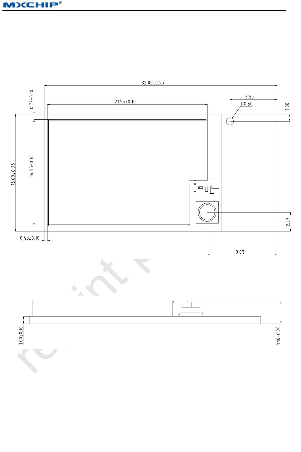
Mechanical dimensions 2.1
EMW3166mechanical dimension of vertical view:
Figure 3 Vertical view
EMW3166 mechanical dimension of side view:
Figure 4 side view
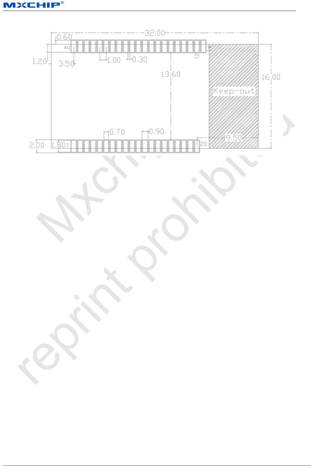
Recommended package design 2.2
The figure followed below is the recommended package design MXCHIP suggested while designing the baseplate.
The solder window has the same size of the pad.
Application Note [Page 11
EMW3166_Guide For User Design
Figure 5 Recommended Package for SMT
DC power design 2.3
Peak current of EMW3166 is about 320mA. The DC/DC power chip MXCHIP recommended should be whose
maximum output current is over 600mA. DC/DC gets more superiority on power conversion than LDO.
When using DC/DC power chip, except for the requirements of output voltage (3.3V) and maximum current
(600mA), application designer should pay more attention on the arrangement of wires. For instance, device should
be compact enough, the ground of input and output should be well connected and the feedback signal should be far
away from the inductance and the Schottky diode. Please refer to the datasheet of DC/DC power chip for more
information.
When using LDO power chip, application designer need notice on the maximum current (600mA) and heat
dissipation.1.4 Recommended circuit design
Set the GND apart from power supply when designing layout to avoid the instantaneous peak current when power
on.
Application Note [Page 12]
EMW3166_Guide For User Design
RF design 2.5
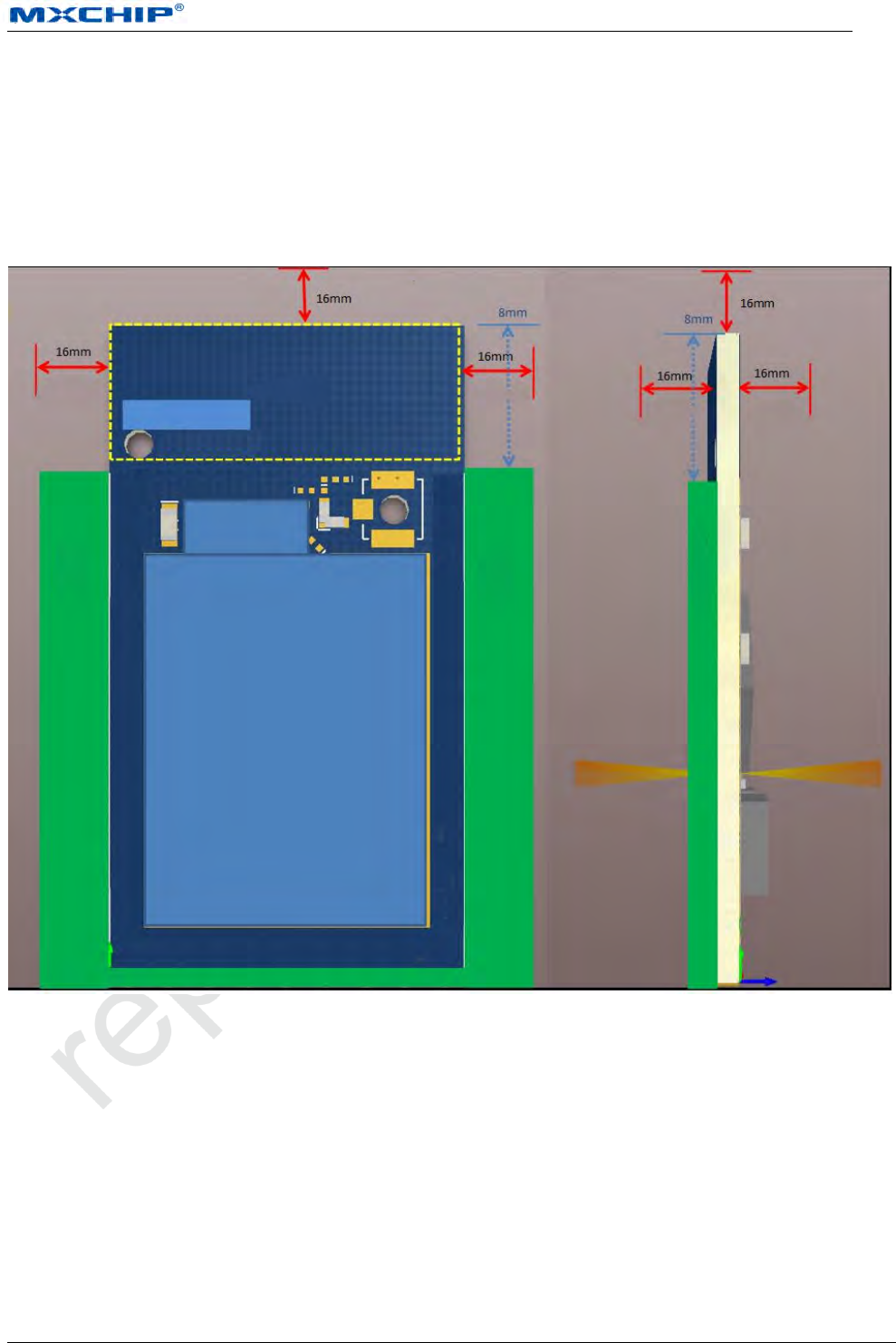
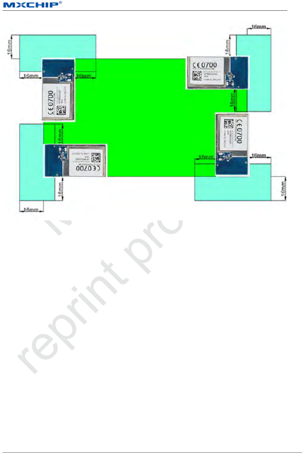
2.5.1 PCB antenna design
When integrating the WiFi module with on board PCB printed antenna, make sure the area around the antenna end
the module protrudes at least 15mm from the mother board PCB and any metal enclosure. The area under the
antenna end of the module should be keep clear of metallic components, connectors, sensors, traces and other
materials that can interfere with the radio signal.
Figure 7 Minimum Size of Keep-out Zone Around Antenna
Areas on the mother board MXCHIP recommended showed below can reduce the noise to PCB antenna and radio
signal.
User
Pad
User
Pad
User pad
Model Number
PCB Antenna
position
Left
headromm
area
Right
headromm
area
Front
headromm
area
Antenna headromm area
distance with user pad
Back
headromm
area
Observe
headromm
area
Front
headromm
area
Application Note [Page 13]
EMW3166_Guide For User Design
Figure 8 Module Position Recommended on Mother Board
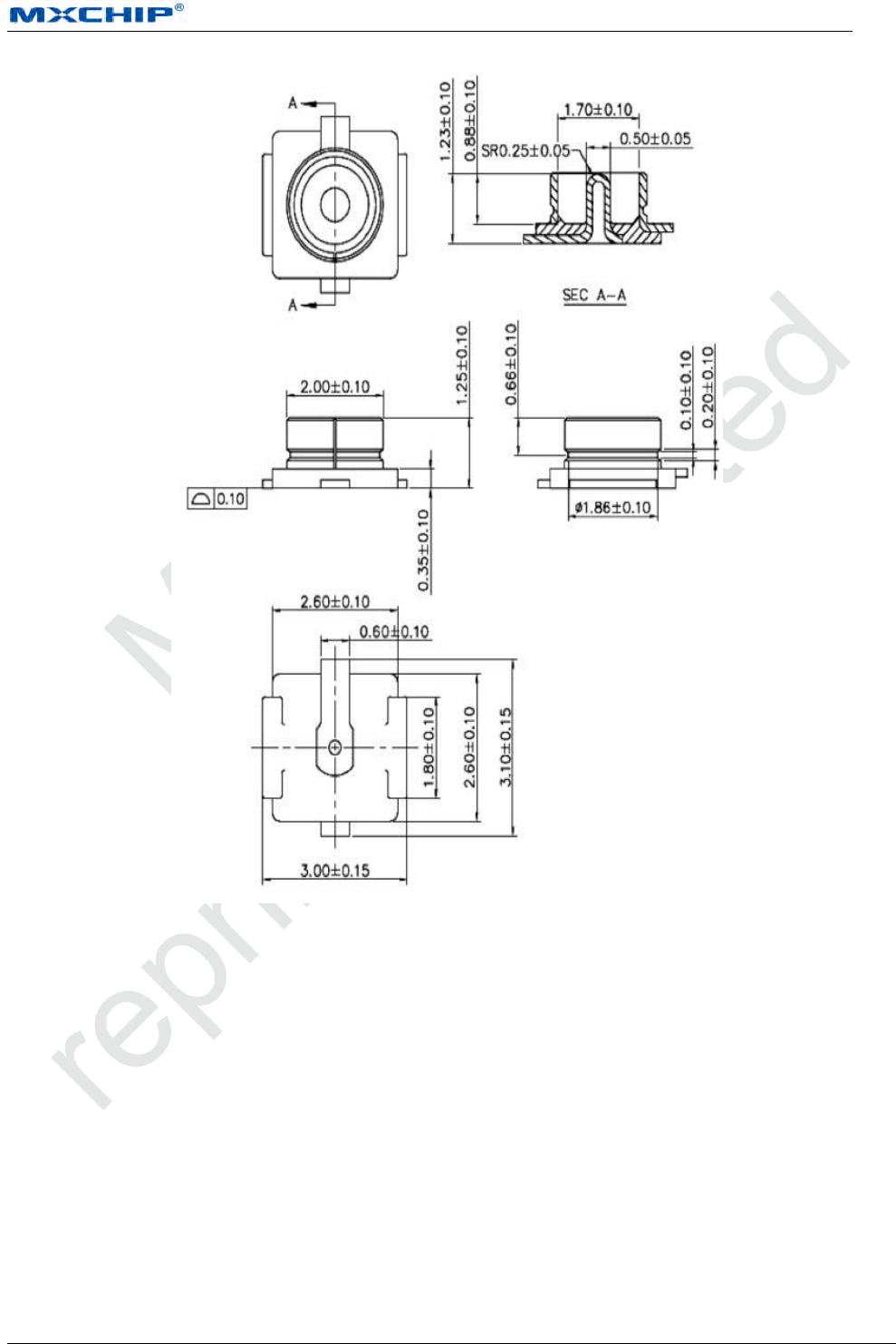
2.5.2 T U.F.L RF Connector
Make sure the connector is matched when choosing the external antenna.
Mechanical dimensions of U.F.L RF connector shows as followed.
Application Note [Page 14]
EMW3166_Guide For User Design
Figure 9 U.F.L Connector Size
ESD design 2.6
ESD grade of module: Human Body Model (HBM) sensitivity is 2000V, Charged Device Model (CDM) sensitivity
is 500V. If a higher ESD level is required, the pins that may be connected to the outside should be reserved place for
the ESD protection device.
If the module connects the mother board by outside leads, application designers should notice the EMI problems.
Using shield cable or reserving the position for common mode choke to solve this problem.
Application Note [Page 15]
EMW3166_Guide For User Design
3. Firmware programming and warehousing detection method
Receiving Inspection Device List 3.1
Auxiliary Equipment list shows below:
Table 1 Warehousing Detection Auxiliary Equipment List
Auxiliary Equipment
Quantity
PC
1(pcs)
Fixture
1(pcs)
EMWE-3166-A V1.0 Development Board
1(pcs)
Note: It is not for sale in above the table Auxiliary Equipment.
Application software and firmware:
FT230XS (drivers on PC), download link:
http://www.ftdichip.com/Drivers/VCP.htm
Programming firmware should be confirmed by both MXCHIP FAE and guests. Its size is
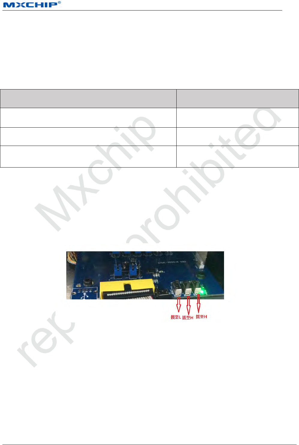
512kbytes. The set of the three toggle switches on EMWE-3166-A V1.0 development board:
Figure 10 Development Board Switch Settings
Collection 3.2
Connect the fixture to the EMWE-3166-A V1.0 development board by the pin header. Connect the EMWE-3166-A
V1.0 development board to PC by USB Mini cable.
Red led lights if connected.
Warehousing detection 3.3
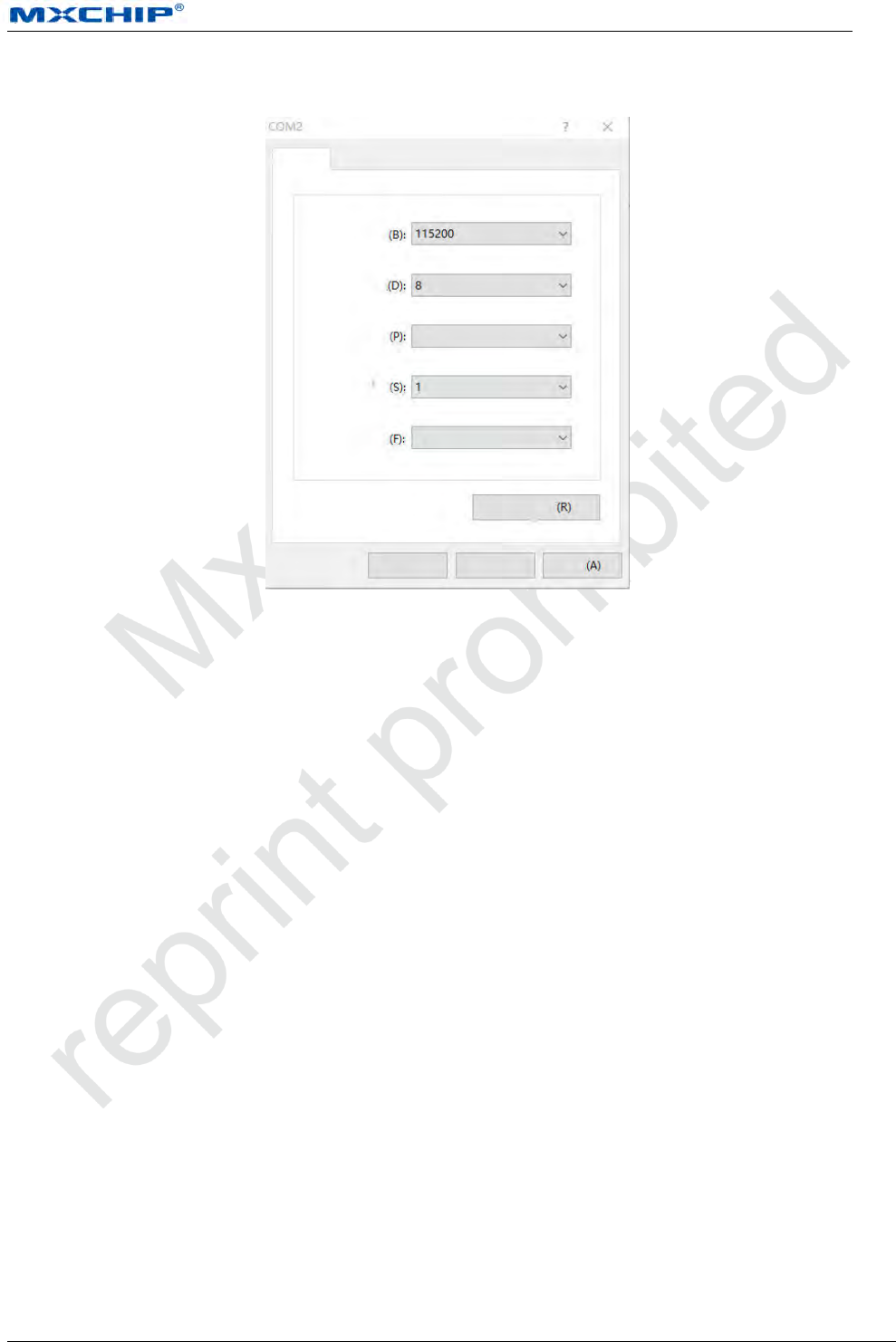
3.3.1 Software setting
Software:Hyper Terminal
Find the COM number where EMW3166 connect with PC in “device manager”.
Application Note [Page 16]
EMW3166_Guide For User Design
Set as followed:
Figure 11 Hyper Terminal Setting Connection
3.3.2 Module testing
Click “connect” in “Hyper Terminal” to connect the PC to EMWE-3166-A V1.0 development
board.
Place the module on the fixture.
Press down the handle.
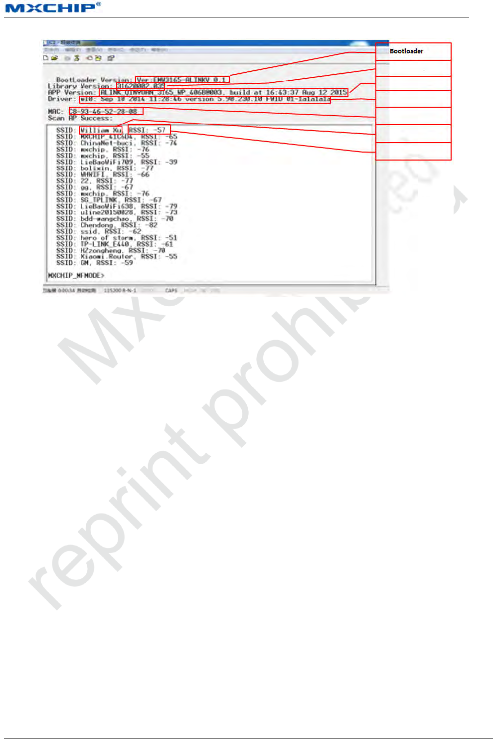
3.3.3 Testing result
It lists the testing result from serial on “Hyper Terminal”. The message includes: bootloader
version, library version, application version, driver version, MAC address, APs’ name and signal
strength.
Set ports
Bit
Data bits
parity
stop
data flow
control
None
None
Reset
Ensure Cancel Apply
Property
Application Note [Page 17]
EMW3166_Guide For User Design
Figure 12 Testing Results
Statements 3.4
MXCHIP has the obligation to guarantee there is no quality problem for the module delivered at each
batch.
If problems are found while sampling module, customer has the right to require MXCHIP to give a timely
replacement.
If problems are found after welding the module on mother board without any warehousing detection,
MXCHIP is only responsible for the compensation of module.
MXCHIP has the obligation to assist solving various technical problems, without retaining any MVA/BIN
file of customer.
Customer has the obligation to record every firmware version during the firmware developing work and
use the proper firmware for production.
version
Liblary version
Application version
Driver version
MAC Address
Hotspot Name
signal strength
Application Note [Page 18]
EMW3166_Guide For User Design
4. SMT matters
Note for stencil aperture 4.1
The recommended stencil aperture: 0.12mm (0.1~0.15mm), laser polishing hole.
The recommended solder paste is SAC305 and lead free.
The recommended extend length of welding pad: 0.15mm. It can enhance the adhesive ability of
solder as shown below.
It can check the right position of the module by eyes if using SMT line without AOI testing to reduce the risk of cold
solder joint.
Figure 13 Recommended Stencil Aperture
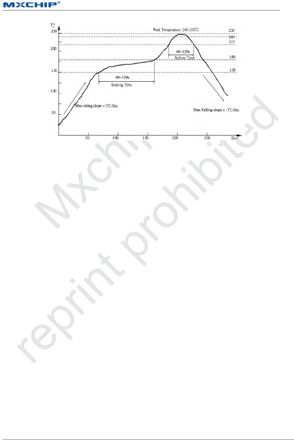
Recommended reflow profile 4.2
Reflow times <= 2 times.
Peak temperature < 250°C.
Controlling the temperature according to the temperature curve can reduce the risk of welding.
Recommended reflow profile:
Application Note [Page 19]
EMW3166_Guide For User Design
Figure 14 Reflow soldering temperature curve

Application Note [Page 20]
EMW3166_Guide For User Design
5. Mass production testing and firmware upgrading
In addition to considering the product features, application designer need to think over how to do
test and upgrade firmware when developing.
Mass production test 5.1
Avoid finding problem after installing the PCB boards in machine
5.1.1 EMSP command way
Connect the module to the MCU of the mother board by serial port and use the EMSP command.
Choose one triggering way---- set one combination key, to send the test command from the MCU. The test command
could be one EMSP command used to scan the APs around or connect one specified AP. The way can test both of the
serial function and the RF function.
5.1.2 Limited development firmware
Connect the module to the MCU of the mother board by serial port. Add the test command in the firmware when
developing. The test command could be one command from serial port used to scan the APs and return the results by
serial port. The way can test both of the serial function and the RF function by using the same triggering way.
5.1.3 Full development firmware
Full development works for the whole application of the project.
Test method could be flexible in the way. It can set a specific way to test every function of the module. The
application determines the specific test details.
Upgrading 5.2
Upgrading by OTA is recommended. OTA-over the air, is one wireless upgrading way.
The upgrading method is offered by MXCHIP. Several application cases are provided as referenced.
Firmware could be upgraded to the latest version by OTA with this upgrading method applied.

Application Note [Page 21]
EMW3166_Guide For User Design
6. Firmware encrypt
In order to make sure the firmware could not be modified after programming in the module, firmware must be
encrypted with the bootloader drivers and the chip ID MXCHIP offered.
Bootloader driver is used to drive the device in the module and integrated with one AES encryption way. The
application part of the firmware must be combined with the bootloader driver to generate one MVA/bin file after
adding the chip ID details which can be used to identify MXCHIP module. Check the official website for more
information.

Application Note [Page 22]
EMW3166_Guide For User Design
7. Sales and technical support information
If you need to buy this product, please call MXCHIP during the working hours.
(Monday ~ Friday : A.M. 9:00~12:00; P.M. 1:00~6:00)
Telephone: +86-021-52655026
Address: 9th Floor, 5# building, Lane 2145, Jinshajiang Road, Putuo District, Shanghai
Post Code: 200333
Email: sales@mxchip.com
Company email: http://www.mxchip.com
For the latest information about products, please refer to: http://www.mxchip.com
Related technical support please contact:
a. Wireless network technology support:
+86 (21) 52655026-812, Email: support@mxchip.com.
b. Technical support for development tools:
+86 (21) 52655026-822, Email: support@mxchip.com.

Application Note [Page 23]
EMW3166_Guide For User Design
8. FCC Statement
FCC identification number is not visible when the device is installed inside another device, then the
outside of the device into which the device is installed must also display a label referring to the enclosed
device. This exterior label can use wording such as the following: “Contains FCC ID:P53- EMW3166”
This device complies with part 15 of the FCC Rules. Operation is subject to the
following two conditions:
(1) This device may not cause harmful interference, and
(2) This device must accept any interference received, including interference that may cause undesired
operation. Changes or modifications not expressly approved by the party responsible for compliance
could void the user's authority to operate the equipment.
NOTE: This equipment has been tested and found to comply with the limits for a Class B digital
device, pursuant to Part 15 of the FCC Rules. These limits are designed to provide reasonable
protection against harmful interference in a residential installation. This equipment generates, uses and
can radiate radio frequency energy and, if not installed and used in accordance with the instructions,
may cause harmful interference to radio communications. However, there is no guarantee that
interference will not occur in a particular installation. If this equipment does cause harmful interference
to radio or television reception, which can be determined byturning the equipment off and on, the user
is encouraged to try to correct the interference by one ormore of the following measures:
This transmitter must not be co‐located or operating in conjunction with any other antenna or transmitter.
This device must be installed and operated with a minimum distance of 20 cm between the radiator and
user body.
-- Reorient or relocate the receiving antenna.
-- Increase the separation between the equipment and receiver.
--Connect the equipment into an outlet on a circuit different from that to which
the receiver is connected.
-- Consult the dealer or an experienced radio/TV technician for help.
Note 1: Compliance of this device in all final host configurations is the responsibility of the Grantee.
OEM integrators are responsible to satisfy RF exposure requirements.
Note 2: Any modifications made to the module will void the Grant of Certification, this module is limited to OEM
installation only and must not be sold to end-users, end-user has no manual instructions to remove or install the
device, only software or operating procedure shall be placed in the end-user operating manual of final products.
Note 3: The device must not transmit simultaneously with any other antenna or transmitter.
Note 4: To ensure compliance with all non-transmitter functions the host manufacturer is responsible for ensuring
compliance with the module(s) installed and fully operational. For example, if a host was previously authorized as
an unintentional radiator under the Declaration of Conformity procedure without a transmitter certified module and
a module is added, the host manufacturer is responsible for ensuring that the after the module is installed and
operational the host continues to be compliant with the Part 15B unintentional radiator requirements. Since this may
depend on the details of how the module is integrated with the host, Shanghai MXCHIP Information Technology
Co., Ltd. shall provide guidance to the host manufacturer for compliance with the Part 15B requirements.
The transmitter module must be installed and used in strict accordance with the manufacturer's instructions as
described in the user documentation that comes with the host product.Shanghai MXCHIP Information Technology
Co., Ltd.is responsible for the compliance of the module in all final hosts.
FCC Radiation Exposure Statement
This device complies with FCC RF radiation exposure limits set forth for an uncontrolled environment.