Meet MS-WMBM1 External Wireless Dongle User Manual
Meet International Ltd. External Wireless Dongle
UserManual.wiki
>
Meet
>
MS WMBM1 User Manual
User manual
Navigation menu
Upload a User Manual
Namespaces
Wiki Guide
HTML
PDF
Info
Views
User Manual
Discussion / Help
Navigation

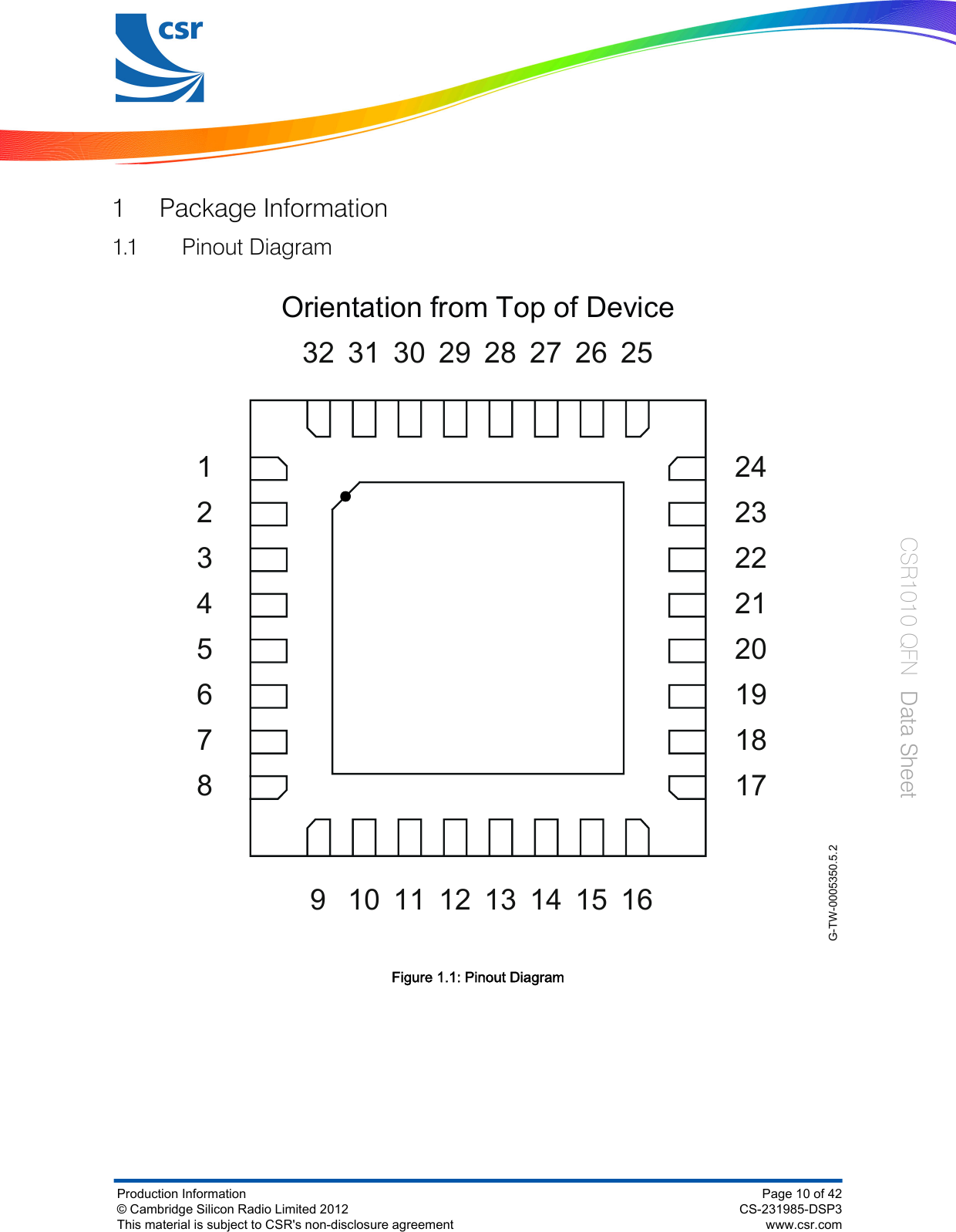
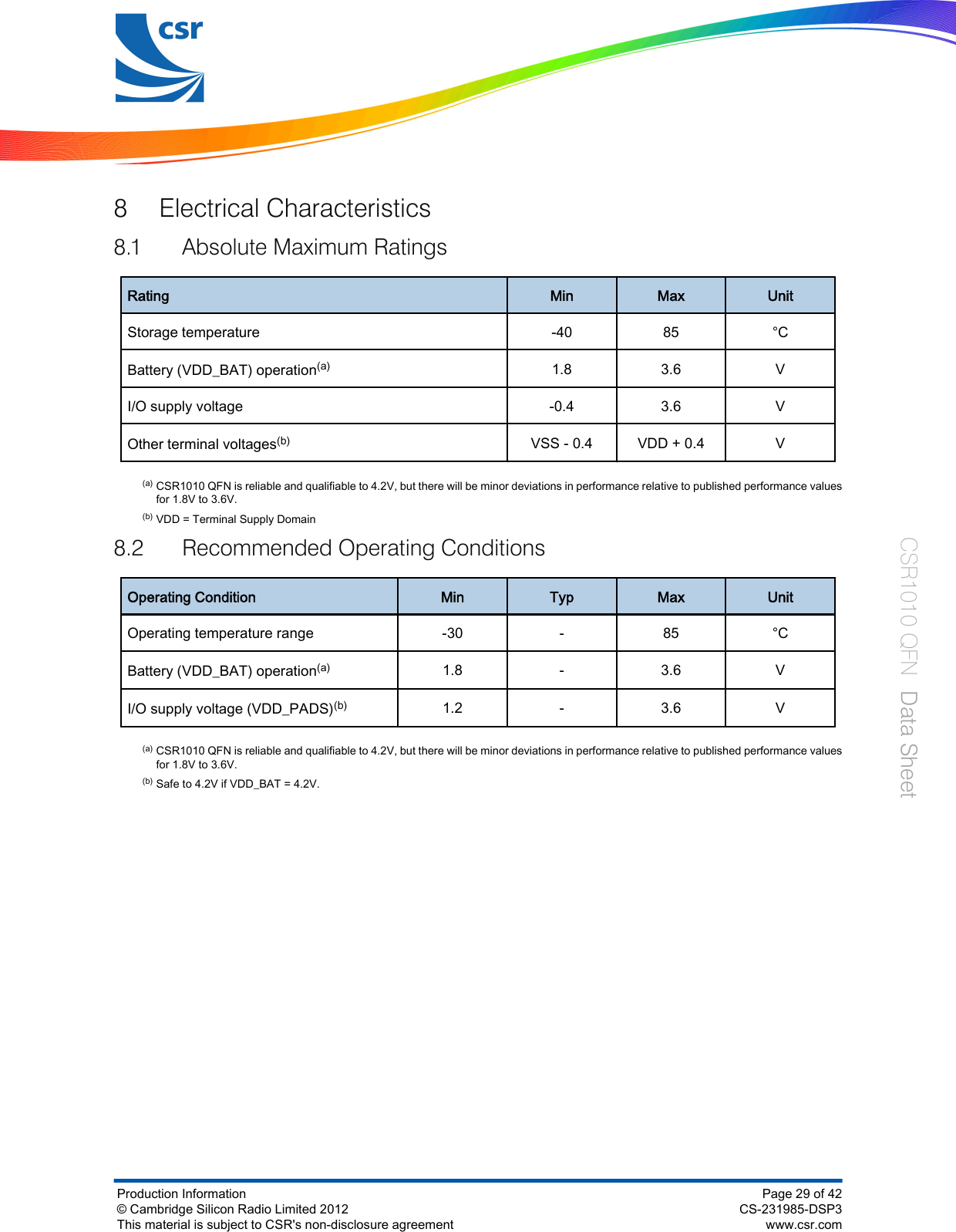
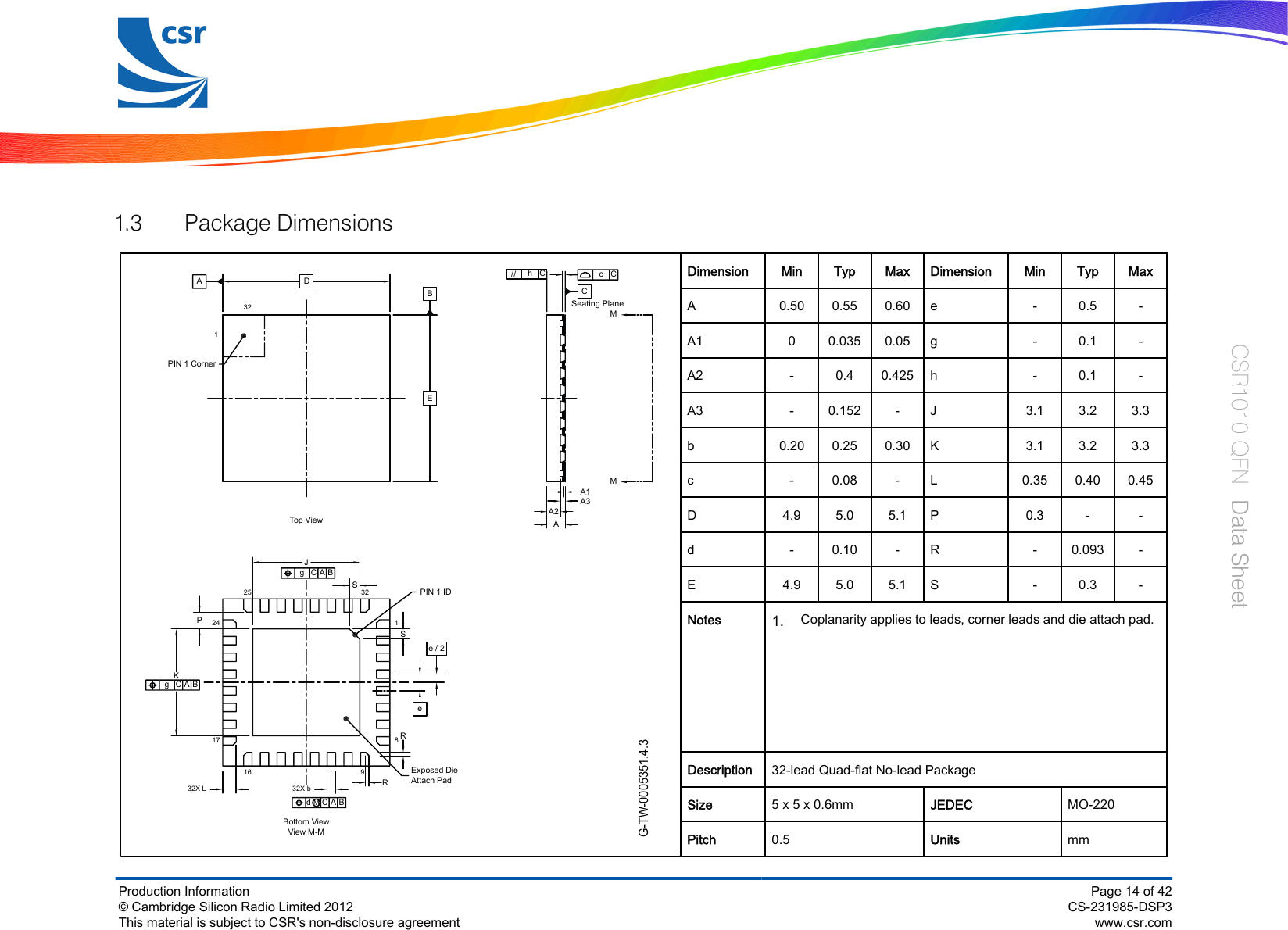
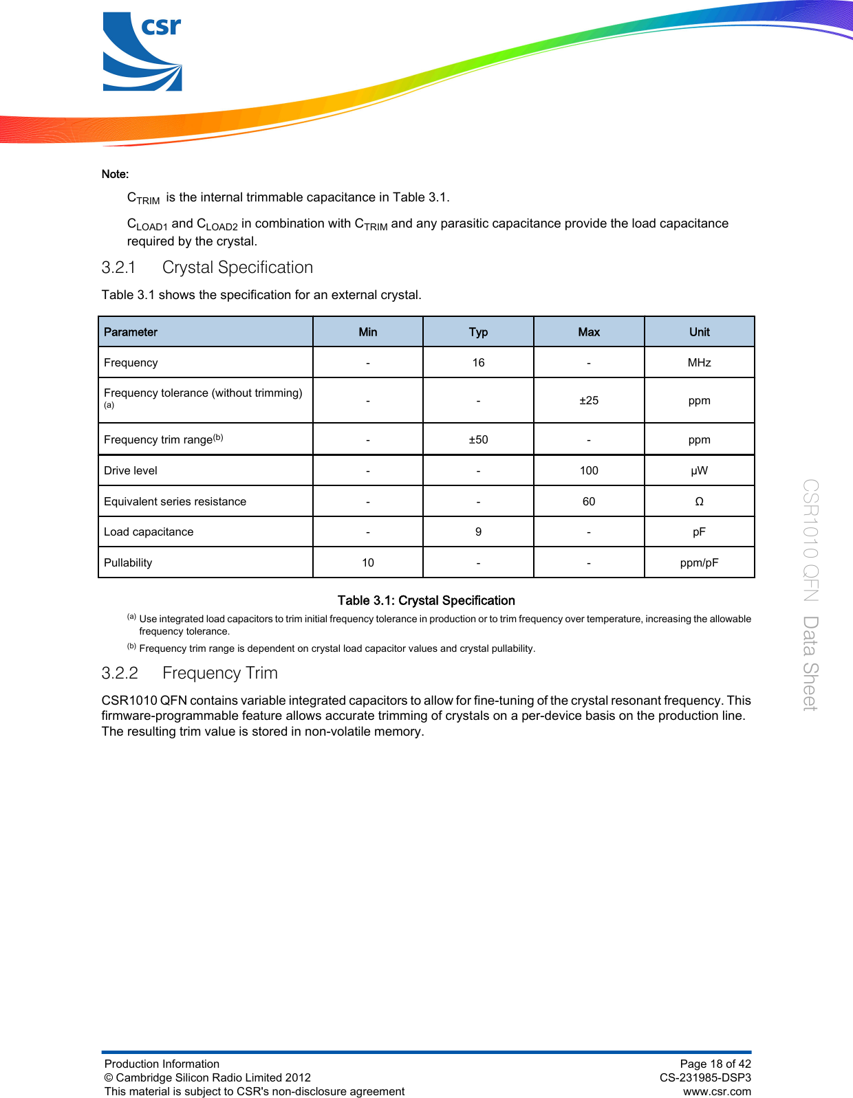
![1.2 Device Terminal FunctionsRadio Lead Pad Type Supply Domain DescriptionRF 7RF VDD_RADIO(a) Bluetooth transmitter / receiver.(a)The VDD_RADIO domain is generated from VDD_REG_IN, see Figure 6.1.Synthesiser andOscillator Lead Pad Type Supply Domain DescriptionXTAL_32K_OUT 2Analogue VDD_BAT Drive for sleep clock crystal.XTAL_32K_IN 3Analogue VDD_BAT 32.768kHz sleep clock input.XTAL_16M_OUT 9Analogue VDD_ANA(b) Drive for crystal.XTAL_16M_IN 10 Analogue VDD_ANA Reference clock input.(b)The VDD_ANA domain is generated from VDD_REG_IN, see Figure 6.1.I²C Interface Lead Pad Type Supply Domain DescriptionI2C_SDA 29Bidirectional, tristate,with weak internalpull-upVDD_PADSI²C data input / output or SPI serialflash data output (SF_DOUT). Ifconnecting to SPI serial flash,connect this pin to SO on the serialflash. See Section 5.3.I2C_SCL 28 Input with weakinternal pull-up VDD_PADS I²C clock or SPI serial flash clockoutput (SF_CLK), see Section 5.3.PIO Port Lead Pad Type Supply Domain DescriptionPIO[11] 25 Bidirectional withprogrammablestrength internal pull-up/downVDD_PADS Programmable I/O line.PIO[10] 24PIO[9] 23Production Information© Cambridge Silicon Radio Limited 2012This material is subject to CSR's non-disclosure agreementPage 11 of 42CS-231985-DSP3www.csr.comCSR1010 QFN Data Sheet](https://usermanual.wiki/Meet/MS-WMBM1/User-Guide-3194366-Page-11.png)
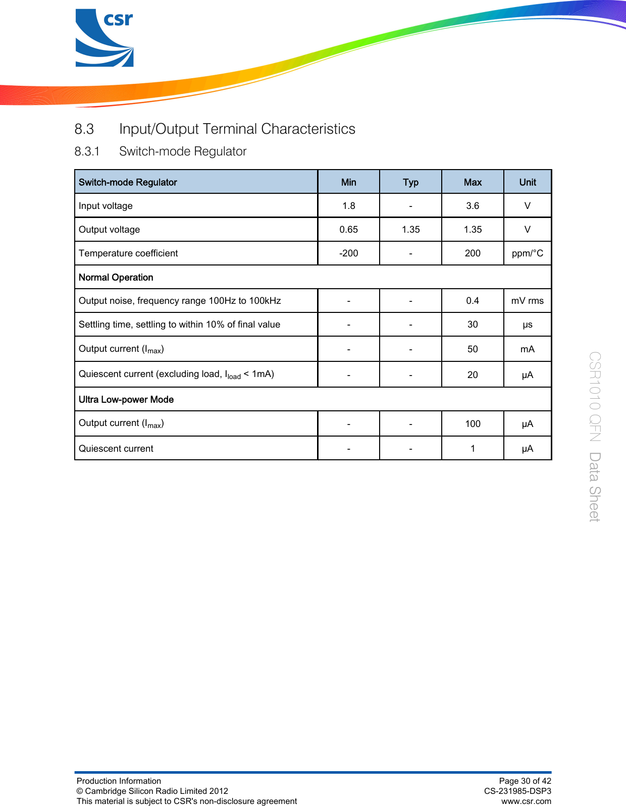
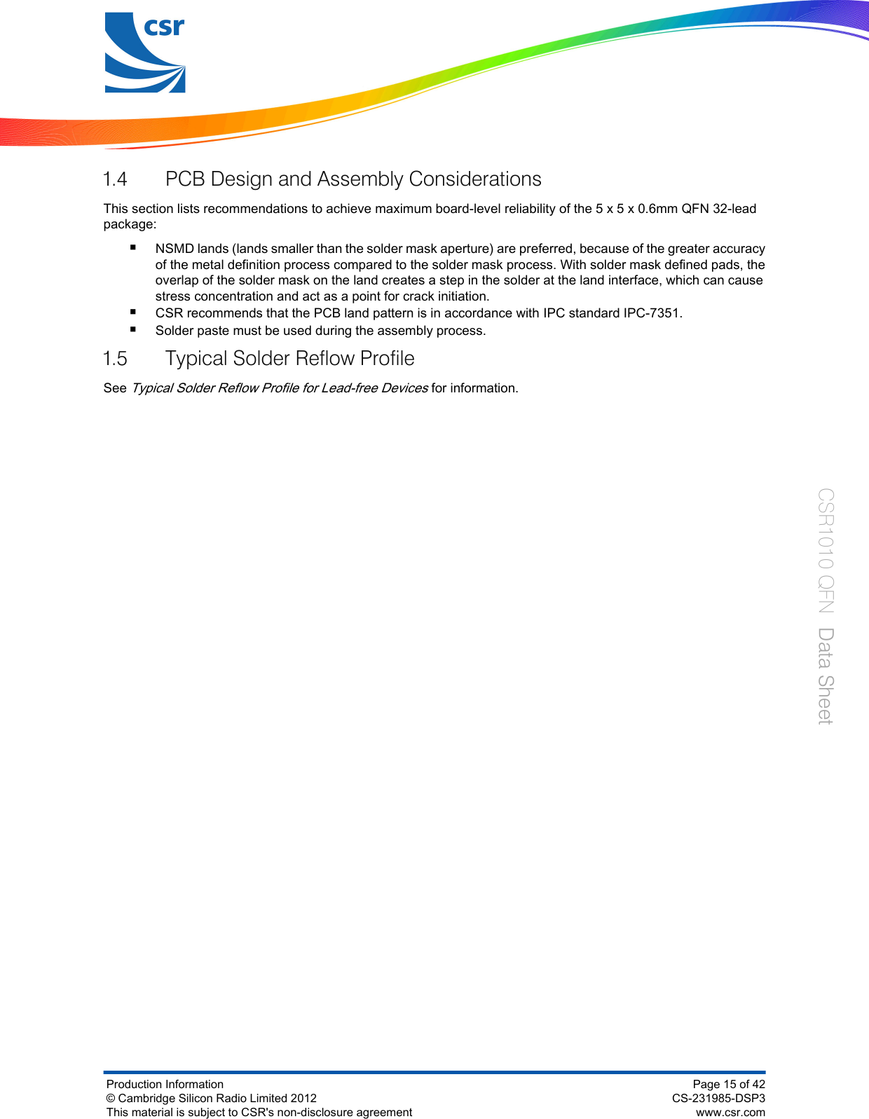
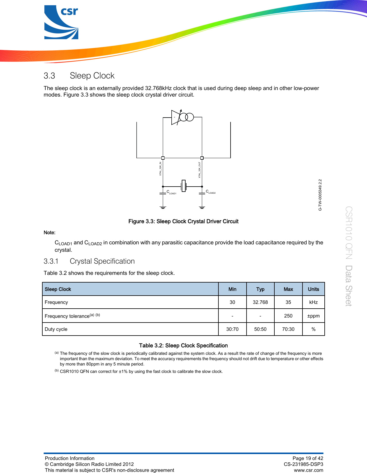
![PIO Port Lead Pad Type Supply Domain DescriptionPIO[8] /DEBUG_MISO 22Bidirectional withprogrammablestrength internal pull-up/downVDD_PADSProgrammable I/O line or debug SPIMISO selected by SPI_PIO#.PIO[7] /DEBUG_MOSI 20 Programmable I/O line or debug SPIMOSI selected by SPI_PIO#.PIO[6] /DEBUG_CS# 19Programmable I/O line or debug SPIchip select (CS#) selected bySPI_PIO#.PIO[5] /DEBUG_CLK 18 Programmable I/O line or debug SPICLK selected by SPI_PIO#.PIO[4] /SF_CS# 17Bidirectional withprogrammablestrength internal pull-up/downVDD_PADSProgrammable I/O line or SPI serialflash chip select (SF_CS#), seeSection 5.3.PIO[3] /SF_DIN 16Programmable I/O line or SPI serialflash data (SF_DIN) input. Ifconnecting to SPI serial flash, thispin connects to SI on the serial flash.See Section 5.3.PIO[2] 27Bidirectional withprogrammablestrength internal pull-up/downVDD_PADS Programmable I/O line or I²C power.PIO[1] /UART_RX 15 Bidirectional withprogrammablestrength internal pull-up/downVDD_PADSProgrammable I/O line or UART RX.PIO[0] /UART_TX 14 Programmable I/O line or UART TX.AIO[2] 11Bidirectionalanalogue VDD_AUX(c) Analogue programmable I/O line.AIO[1] 12AIO[0] 13(c)The VDD_AUX domain is generated from VDD_REG_IN, see Figure 6.1.Test and Debug Lead Pad Type Supply Domain DescriptionSPI_PIO# 26 Input with stronginternal pull-down VDD_PADS Selects SPI debug on PIO[8:5].Production Information© Cambridge Silicon Radio Limited 2012This material is subject to CSR's non-disclosure agreementPage 12 of 42CS-231985-DSP3www.csr.comCSR1010 QFN Data Sheet](https://usermanual.wiki/Meet/MS-WMBM1/User-Guide-3194366-Page-12.png)
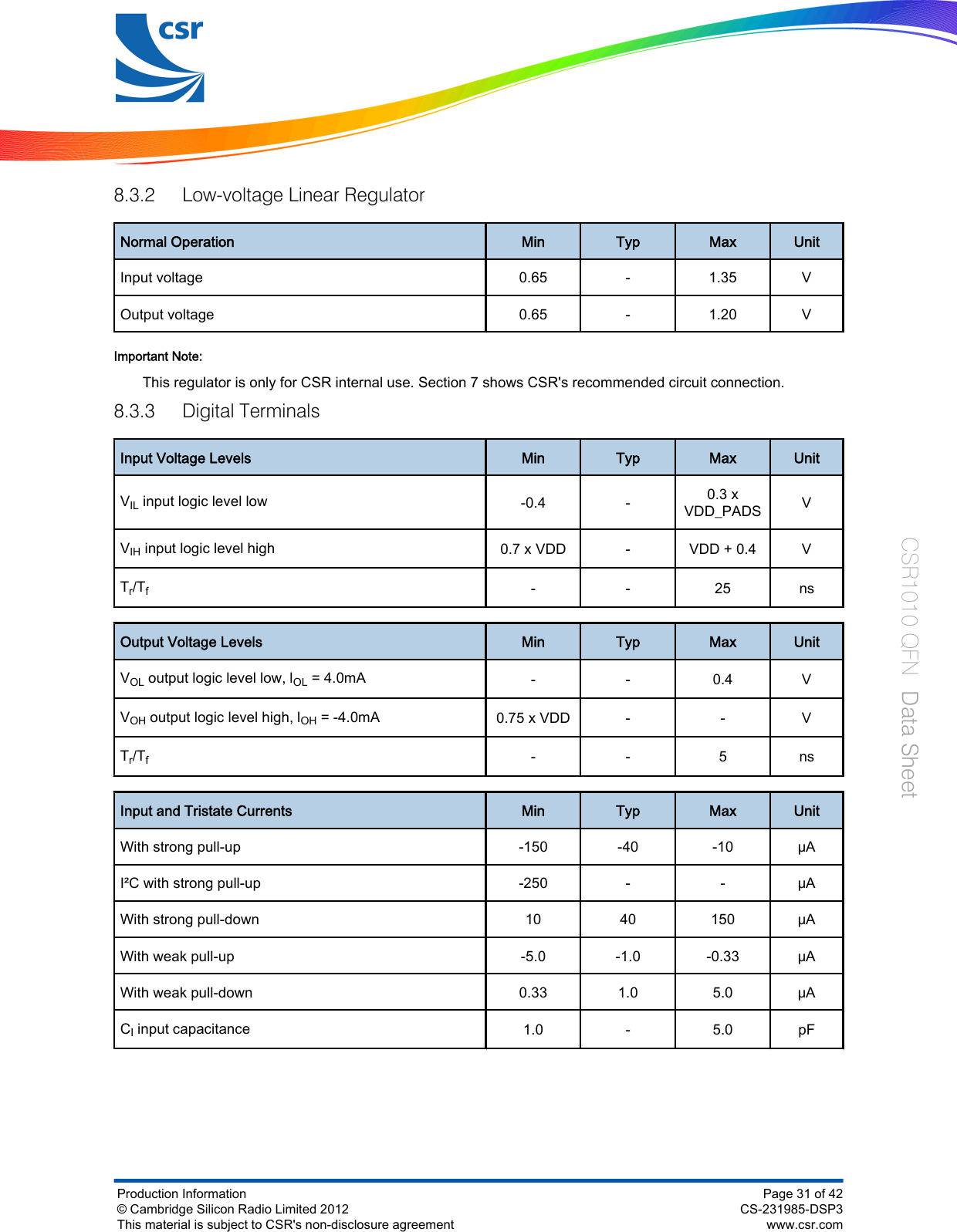
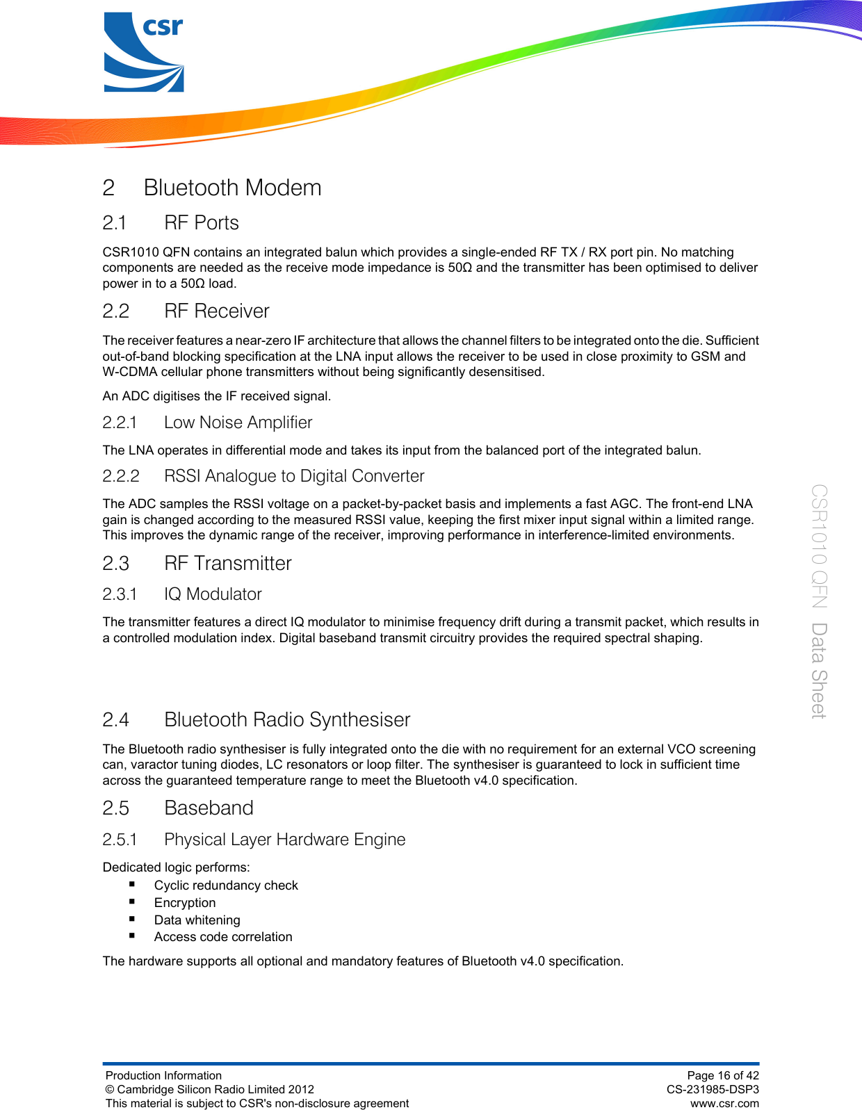
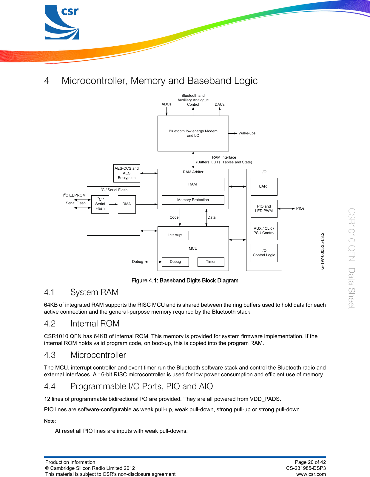
![Wake-up Lead Pad Type Supply Domain DescriptionWAKE 4Input has no internalpull-up or pull-down,use external pull-down.VDD_BAT Input to wake CSR1010 QFN fromhibernate or dormant.Power Supplies andControl Lead DescriptionVDD_BAT 1Battery input and regulator enable (active high).VDD_BAT_SMPS 32 Input to high-voltage switch-mode regulator.SMPS_LX 31 High-voltage switch-mode regulator output.VDD_CORE 5, 30 Positive supply for digital domain.VDD_PADS 21 Positive supply for all digital I/O ports PIO[11:0].VDD_REG_IN 6Positive supply for Bluetooth radio and digital linearregulator.VDD_XTAL 8Decouple with 470nF capacitor to ground.VSS Exposed pad Ground connections.Production Information© Cambridge Silicon Radio Limited 2012This material is subject to CSR's non-disclosure agreementPage 13 of 42CS-231985-DSP3www.csr.comCSR1010 QFN Data Sheet](https://usermanual.wiki/Meet/MS-WMBM1/User-Guide-3194366-Page-13.png)
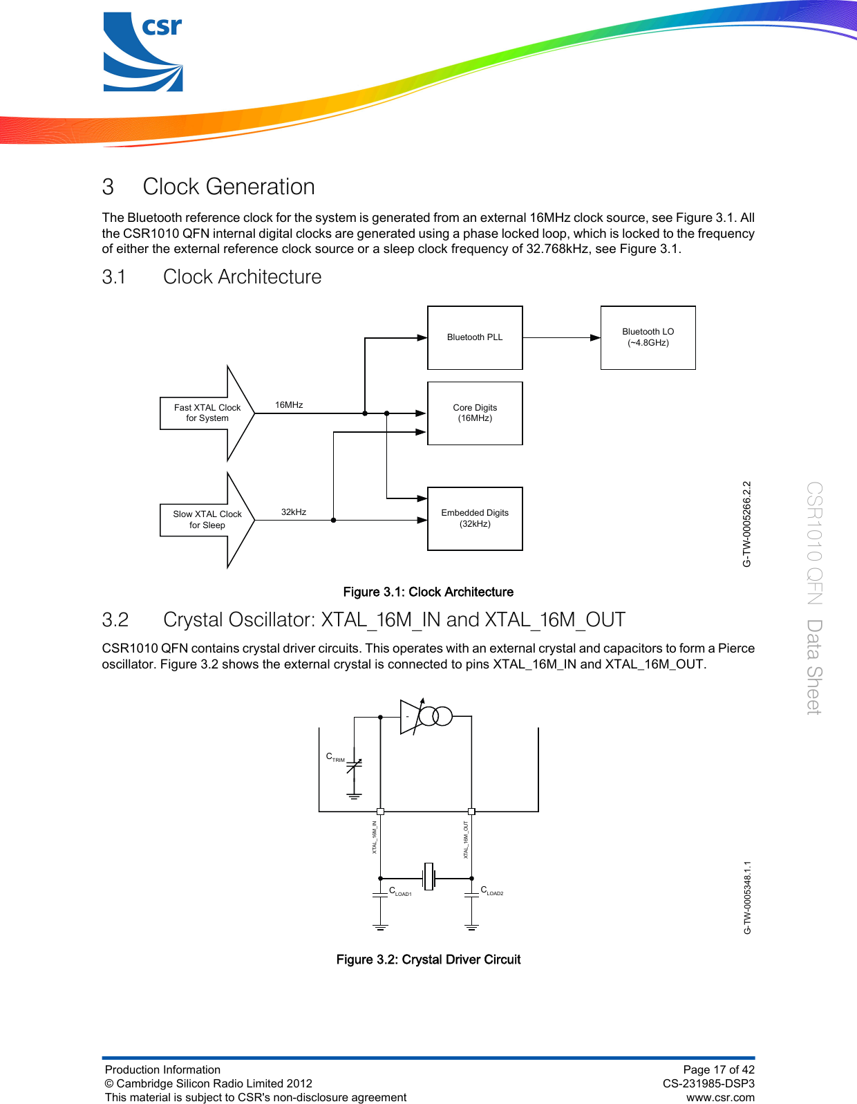
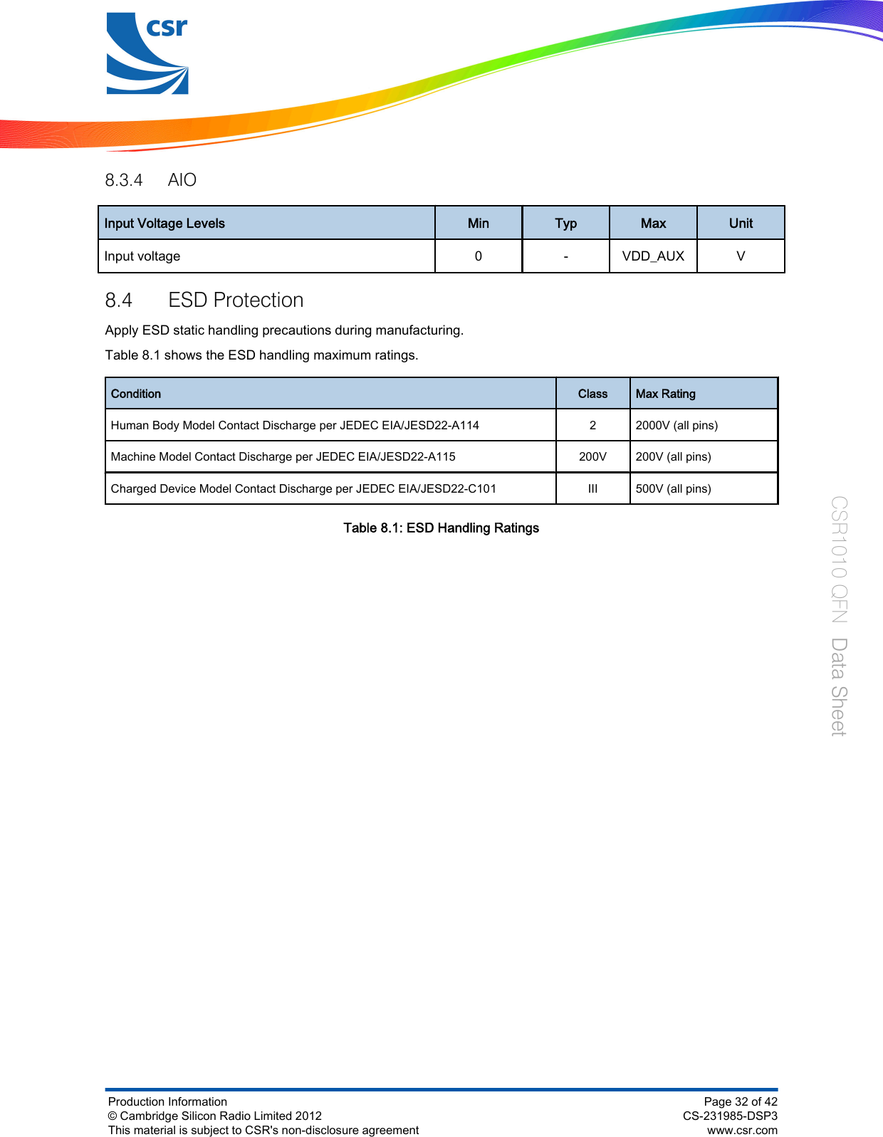
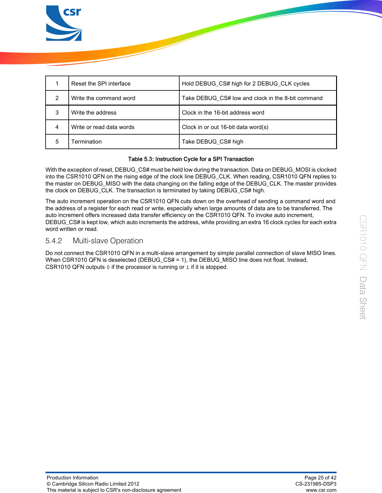
![Any of the PIO lines can be configured as interrupt request lines or to wake the IC from deep sleep mode. Table4.1 lists the options for waking the IC from the sleep modes.Sleep Mode Wake-up OptionsDormant Can only be woken by the WAKE pin.Hibernate Can be woken by the WAKE pin or by the watchdog timer.Deep Sleep Can be woken by any PIO configured to wake the IC.Table 4.1: Wake Options for Sleep ModesThe CSR1010 QFN supports alternative functions on the PIO lines:■SPI interface, see Section 1.2 and Section 5.4■UART, see Section 1.2 and Section 5.1.1■LED flasher / PWM module, see Section 4.5Note:CSR cannot guarantee that the PIO assignments remain as described. Implementation of the PIO lines isfirmware build-specific, for more information see the relevant software release note.CSR1010 QFN has 3 general-purpose analogue interface pins, AIO[2:0].4.5 LED Flasher / PWM ModuleCSR1010 QFN contains a LED flasher / PWM module that works in sleep modes.These functions are controlled by the on-chip firmware.Production Information© Cambridge Silicon Radio Limited 2012This material is subject to CSR's non-disclosure agreementPage 21 of 42CS-231985-DSP3www.csr.comCSR1010 QFN Data Sheet](https://usermanual.wiki/Meet/MS-WMBM1/User-Guide-3194366-Page-21.png)
![5 Serial Interfaces5.1 Application Interface5.1.1 UART InterfaceThe CSR1010 QFN UART interface provides a simple mechanism for communicating with other serial devices usingthe RS232 protocol.2 signals implement the UART function, UART_TX and UART_RX. When CSR1010 QFN is connected to anotherdigital device, UART_RX and UART_TX transfer data between the 2 devices.UART configuration parameters, e.g. baud rate and data format, are set using CSR1010 QFN firmware.When selected in firmware PIO[0] is assigned to a UART_TX output and PIO[1] is assigned to a UART_RX input,see Section 1.2.The UART CTS and RTS signals can be assigned to any PIO pin by the on-chip firmware.Note:To communicate with the UART at its maximum data rate using a standard PC, the PC requires an acceleratedserial port adapter card.Table 5.1 shows the possible UART settings for the CSR1010 QFN.Parameter Possible ValuesBaud rate Minimum1200 baud (≤2%Error)9600 baud (≤1%Error) Maximum 2Mbaud (≤1%Error)Flow control CTS / RTSParity None, Odd or EvenNumber of stop bits 1 or 2Bits per byte 8Table 5.1: Possible UART Settings5.1.1.1 UART Configuration While in Deep SleepThe maximum baud rate is 9600 baud during deep sleep.5.2 I²C InterfaceThe I²C interface communicates to EEPROM, external peripherals or sensors. An external EEPROM connectioncan hold the program code externally to the CSR1010 QFN.Production Information© Cambridge Silicon Radio Limited 2012This material is subject to CSR's non-disclosure agreementPage 22 of 42CS-231985-DSP3www.csr.comCSR1010 QFN Data Sheet](https://usermanual.wiki/Meet/MS-WMBM1/User-Guide-3194366-Page-22.png)
![Figure 5.1 shows an example of an EEPROM connected to the I²C interface where I2C_SCL, I2C_SDA and PIO[2]are connected to the external EEPROM. The PIO[2] pin supplies the power to the EEPROM supply pin, e.g. VDD.At boot-up, if there is no valid ROM image in the CSR1010 QFN ROM area the CSR1010 QFN tries to boot fromthe I²C interface, see Figure 5.2. This involves reading the code from the external EEPROM and loading it into theinternal CSR1010 QFN RAM.G-TW-0005553.1.1VDDWPSCLSDAA0A1A2VSSI2C_SCLI2C_SDAPIO[2]1234567824AA512Figure 5.1: Example of an I²C Interface EEPROM Connection5.3 SPI Master InterfaceThe SPI master memory interface in the CSR1010 QFN is overlaid on the I²C interface and uses a further 3 PIOsfor the extra pins, see Table 5.2.SPI Flash Interface PinFlash_VDD PIO[2]SF_DIN PIO[3]SF_CS# PIO[4]SF_CLK I2C_SCLSF_DOUT I2C_SDATable 5.2: SPI Master Serial Flash Memory InterfaceNote:If an application using CSR1010 QFN is designed to boot from SPI serial flash, it is possible for the firmware tomap the I²C interface to alternative PIOs.The boot-up sequence for CSR1010 QFN is controlled by hardware and firmware. Figure 5.2 shows the sequenceof loading RAM with content from RAM, EEPROM and SPI serial flash.Production Information© Cambridge Silicon Radio Limited 2012This material is subject to CSR's non-disclosure agreementPage 23 of 42CS-231985-DSP3www.csr.comCSR1010 QFN Data Sheet](https://usermanual.wiki/Meet/MS-WMBM1/User-Guide-3194366-Page-23.png)
![G-TW-0005552.2.2Device StartsHardware Copies Content of ROM to RAMHardware Checks I 2C Interface (Default Pins )Presence of EEPROM DeviceHardware Checks SPI Interface ( D efault Pins )Presence of SPI Serial Flash D eviceStar t M CU Executing from RAMCopy Content of SPI Ser i al Flash to RAMCopy Content of EEPROM to RAMYesNoYesNoFigure 5.2: Memory Boot-up Sequence5.4 Programming and Debug InterfaceImportant Note:The CSR1010 QFN debug SPI interface is available in SPI slave mode to enable an external MCU to programand control the CSR1010 QFN, generally via libraries or tools supplied by CSR. The protocol of this interfaceis proprietary. The 4 SPI debug lines directly support this function.The SPI programs, configures and debugs the CSR1010 QFN. It is required in production. Ensure the 4 SPIsignals are brought out to either test points or a header.Take SPI_PIO#_SEL high to enable the SPI debug feature on PIO[8:5].CSR1010 QFN uses a 16-bit data and 16-bit address programming and debug interface. Transactions occur whenthe internal processor is running or is stopped.Data is written or read one word at a time, or the auto-increment feature is available for block access.5.4.1 Instruction CycleThe CSR1010 QFN is the slave and receives commands on DEBUG_MOSI and outputs data on DEBUG_MISO.Table 5.3 shows the instruction cycle for a SPI transaction.Production Information© Cambridge Silicon Radio Limited 2012This material is subject to CSR's non-disclosure agreementPage 24 of 42CS-231985-DSP3www.csr.comCSR1010 QFN Data Sheet](https://usermanual.wiki/Meet/MS-WMBM1/User-Guide-3194366-Page-24.png)
![6.3.1 Digital Pin States on ResetTable 6.1 shows the pin states of CSR1010 QFN on reset. PU and PD default to weak values unless specifiedotherwise.Pin Name / Group On ResetI2C_SDA Strong PUI2C_SCL Strong PUPIO[11:0] Weak PDTable 6.1: Pin States on Reset6.3.2 Power-on ResetTable 6.2 shows how the power-on reset occurs.Power-on Reset Typ UnitReset release on VDD_DIG rising 1.05VReset assert on VDD_DIG falling 1.00Reset assert on VDD_DIG falling (Sleep mode) 0.60Hysteresis 50 mVTable 6.2: Power-on ResetProduction Information© Cambridge Silicon Radio Limited 2012This material is subject to CSR's non-disclosure agreementPage 27 of 42CS-231985-DSP3www.csr.comCSR1010 QFN Data Sheet](https://usermanual.wiki/Meet/MS-WMBM1/User-Guide-3194366-Page-27.png)