Meet MS-WMBM1 External Wireless Dongle User Manual
Meet International Ltd. External Wireless Dongle
Meet >
User manual
Features CSR μEnergy
®
CSR1010
™
QFN
■
128KB memory: 64KB RAM and 64KB ROM
■
Bluetooth® v4.0 specification
■
■
-92.5dBm Bluetooth low energy receive
sensitivity
■
Support for Bluetooth v4.0 specification host
stack including ATT, GATT, SMP, L2CAP, GAP
■
RSSI monitoring for proximity applications
■
<600nA current consumption in dormant mode
■
32kHz and 16MHz crystal or system clock
■
Switch-mode power supply
■
Programmable general purpose PIO controller
■
10-bit ADC
■
12 digital PIOs
■
3 analogue AIOs
■
UART
■
I²C / SPI for EEPROM / flash memory ICs and
peripherals
■
Debug SPI
■
4 PWM modules
■
Wake-up interrupt and watchdog timer
■
QFN 32-lead, 5 x 5 x 0.6mm, 0.5mm pitch
Bluetooth low energy Single-mode IC
Production Information
CSR1010A05
Issue 3
General Description
CSR1010 QFN is a CSR µEnergy platform device.
CSR µEnergy are CSR's single-mode Bluetooth low
energy products for the Bluetooth Smart market.
CSR1010 QFN increases application code and data
space for greater application development flexibility.
CSR μEnergy enables ultra low-power connectivity
and basic data transfer for applications previously
limited by the power consumption, size constraints and
complexity of other wireless standards. The CSR
μEnergy platform provides everything required to
create a Bluetooth low energy product with RF,
baseband, MCU, qualified Bluetooth v4.0 stack and
customer application running on a single IC.
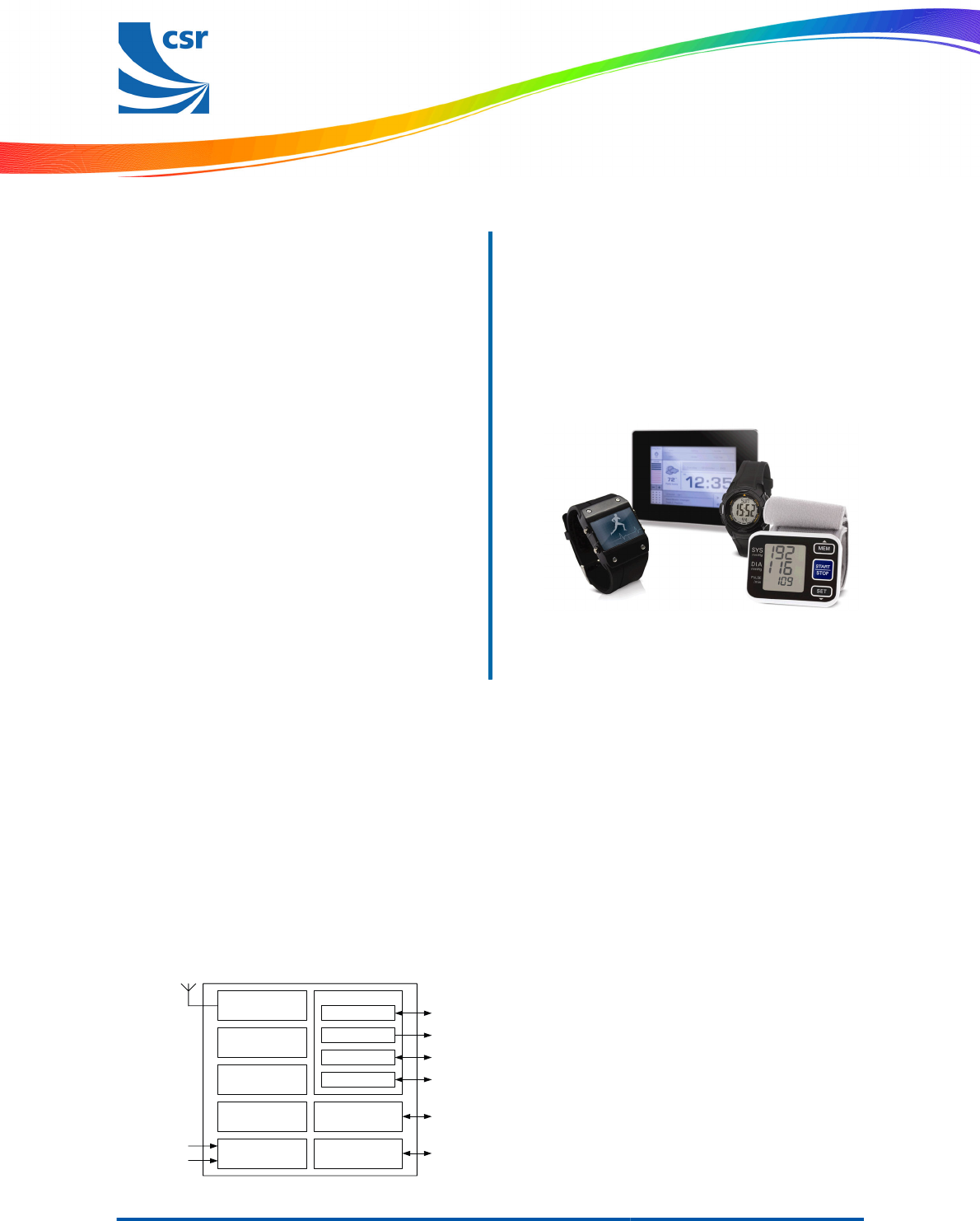
Clock
Generation I
2
C / SPI
Bluetooth LE
Radio and Modem
MCU
I/O
LED PWM
PIO
AIO
UART
DebugRAM
ROM
16MHz
32kHz
Applications
■
Building an ecosystem using Bluetooth low
energy
CSR is the industry leader for Bluetooth low energy,
also known as Bluetooth Smart. Bluetooth Smart
enables connectivity and data transfer to leading
smartphone, tablet and personal computing devices
including Apple iPhone, iPad, iPod and Mac products
and leading Android devices.
Bluetooth low energy takes less time to make a
connection than conventional Bluetooth wireless
technology and can consume approximately 1/20th of
the power of Bluetooth Basic Rate. CSR1010 QFN
supports profiles for health and fitness sensors,
watches, keyboards, mice and remote controls.
Typical Bluetooth Smart applications:
■
HID: keyboards, mice, touchpads, remote
controls
■
Sports and fitness sensors: heart rate, runner
speed and cadence, cycle speed and cadence
■
Health sensors: blood pressure, thermometer and
glucose meters
■
Mobile accessories: watches, proximity tags, alert
tags and camera controls
■
Smart home: heating control and lighting control
Production Information
© Cambridge Silicon Radio Limited 2012
This material is subject to CSR's non-disclosure agreement
Page 1 of 42
CS-231985-DSP3
www.csr.com
CSR1010 QFN
Data Sheet
Ordering Information
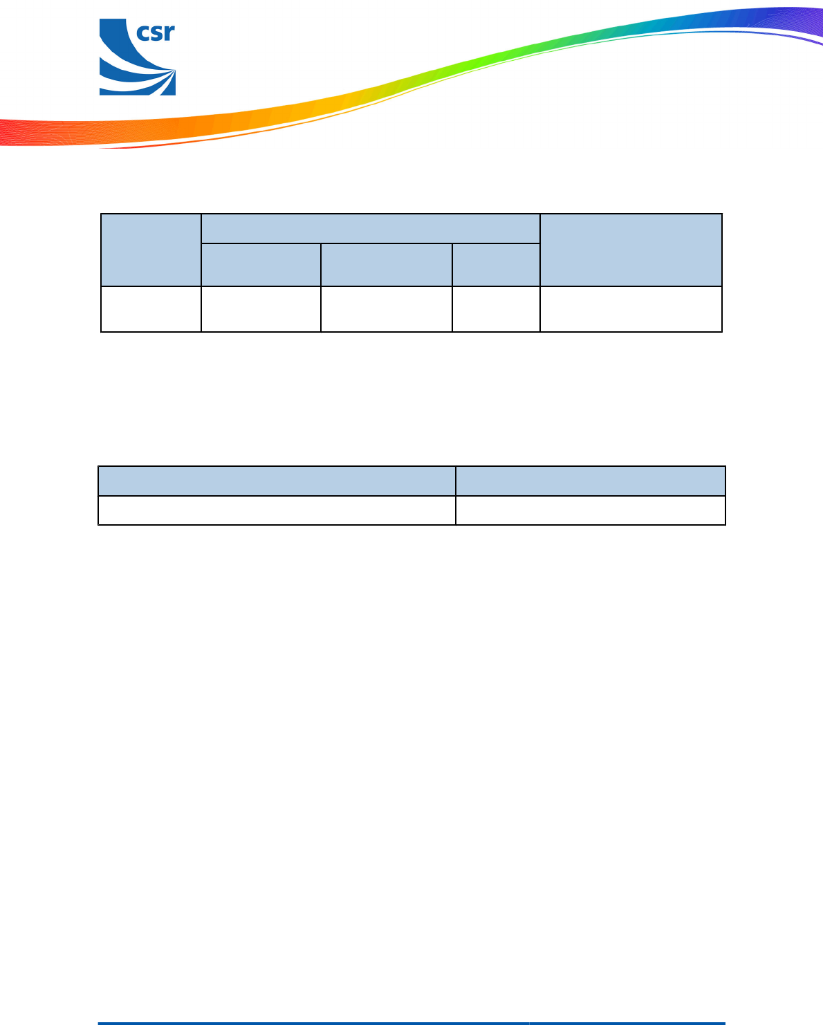
Device
Package
Order Number
Type Size Shipment
Method
CSR1010 QFN QFN‑32-lead
(Pb free)
5 x 5 x 0.6mm
0.5mm pitch Tape and reel CSR1010A05-IQQM-R
Note:
The minimum order quantity is 2kpcs taped and reeled.
Supply chain: CSR's manufacturing policy is to multisource volume products. For further details, contact your
local sales account manager or representative.
CSR1010 QFN Development Kit Ordering Information
Description Order Number
CSR1010 QFN Development Kit example design DK-CSR1010-10138-1A
Contacts
General information
Information on this product
Customer support for this product
Details of compliance and standards
Help with this document
www.csr.com
Sales@csr.com
www.csrsupport.com
Product.compliance@csr.com
Comments@csr.com
Production Information
© Cambridge Silicon Radio Limited 2012
This material is subject to CSR's non-disclosure agreement
Page 2 of 42
CS-231985-DSP3
www.csr.com
CSR1010 QFN
Data Sheet

Device Details
Bluetooth Radio
■
On-chip balun (50Ω impedance in TX and RX
modes)
■
No external trimming is required in production
■
Bluetooth v4.0 specification compliant
Bluetooth Transmitter
■
No external power amplifier or TX/RX switch
required
Bluetooth Receiver
■
-92.5dBm sensitivity
■
Integrated channel filters
■
Digital demodulator for improved sensitivity and co-
channel rejection
■
Fast AGC for enhanced dynamic range
Bluetooth Stack
CSR's protocol stack runs on the integrated MCU:
■
Support for Bluetooth v4.0 specification features:
■
Master and slave operation
■
Including encryption
■
Software stack in firmware includes:
■
GAP
■
L2CAP
■
Security manager
■
Attribute protocol
■
Attribute profile
■
Bluetooth low energy profile support
Synthesiser
■
Fully integrated synthesiser requires no external
VCO varactor diode, resonator or loop filter
Baseband and Software
■
Hardware MAC for all packet types enables packet
handling without the need to involve the MCU
Physical Interfaces
■
SPI master interface
■
SPI programming and debug interface
■
I²C
■
Digital PIOs
■
Analogue AIOs
■
UART
Auxiliary Features
■
Battery monitor
■
Power management features include software
shutdown and hardware wake-up
■
CSR1010 QFN can run in low power modes from an
external 32.768kHz clock signal
■
Integrated switch-mode power supply
■
Linear regulator (internal use only)
■
Power-on-reset cell detects low supply voltage
Package
■
32-lead 5 x 5 x 0.6mm, 0.5mm pitch QFN
Production Information
© Cambridge Silicon Radio Limited 2012
This material is subject to CSR's non-disclosure agreement
Page 3 of 42
CS-231985-DSP3
www.csr.com
CSR1010 QFN
Data Sheet
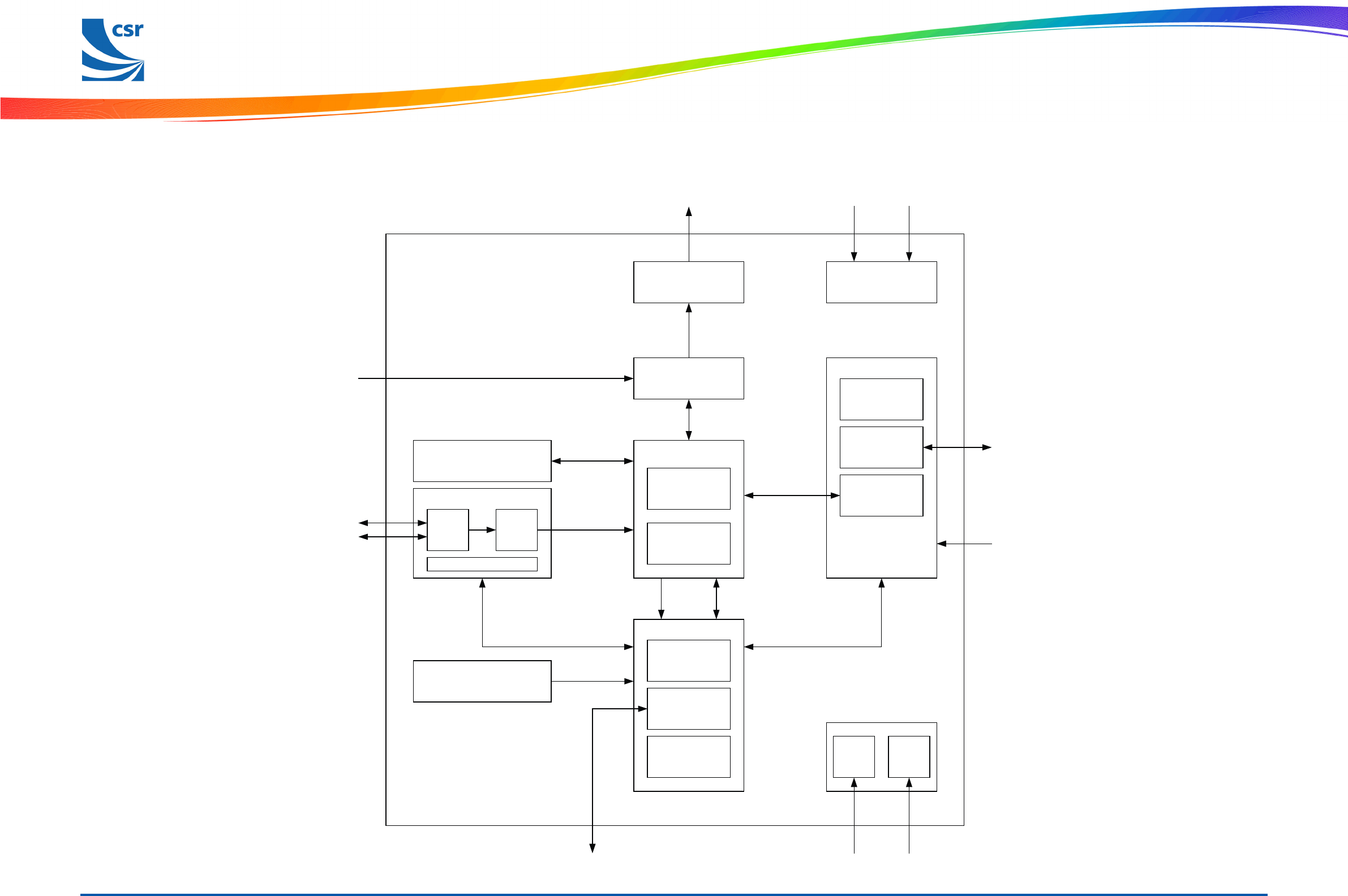
Functional Block Diagram
G-TW-0005362.7.2
I
2
C EEPROM
RF
UART
AUX / CLK /
PSU Control
PIO and LED
PWM
I/O
Clock Generation
SMPULDO
Blutetooth LE Modem
and LC
Bluetooth Radio
RAM 64KB
RAM Arbiter
Memory
Protection
MCU
Interrupt
Debug
Timer
AES-CCS and
AES Encryption
I
2
C / SPI Serial Flash
DMA
I
2
C / SPI
Serial
Flash
Control State Machine
ROM
DataCode
Debug
Wake-up
XTAL_16M XTAL_32K
PIO
VDD_PADS
VDDREG_IN VDD_BAT
SPI Serial Flash
Production Information
© Cambridge Silicon Radio Limited 2012
This material is subject to CSR's non-disclosure agreement
Page 4 of 42
CS-231985-DSP3
www.csr.com
CSR1010 QFN Data Sheet
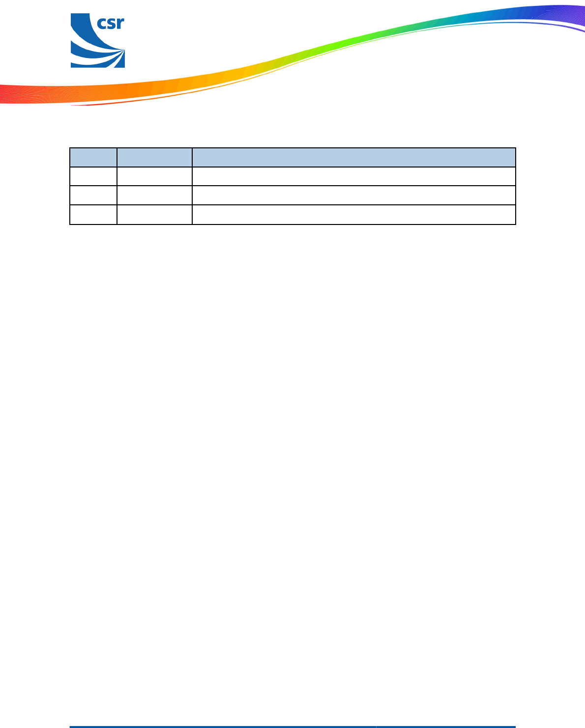
Document History
Revision Date Change Reason
121 SEP 12 Original publication of this document.
223 OCT 12 Updated to Production Information.
320 NOV 12 Update to CSR µEnergy® branding.
Production Information
© Cambridge Silicon Radio Limited 2012
This material is subject to CSR's non-disclosure agreement
Page 5 of 42
CS-231985-DSP3
www.csr.com
CSR1010 QFN Data Sheet

Status Information
The status of this Data Sheet is Production Information.
CSR Product Data Sheets progress according to the following format:
Advance Information
Information for designers concerning CSR product in development. All values specified are the target values of the
design. Minimum and maximum values specified are only given as guidance to the final specification limits and must
not be considered as the final values.
All detailed specifications including pinouts and electrical specifications may be changed by CSR without notice.
Pre-production Information
Pinout and mechanical dimension specifications finalised. All values specified are the target values of the design.
Minimum and maximum values specified are only given as guidance to the final specification limits and must not be
considered as the final values.
All electrical specifications may be changed by CSR without notice.
Production Information
Final Data Sheet including the guaranteed minimum and maximum limits for the electrical specifications.
Production Data Sheets supersede all previous document versions.
Life Support Policy and Use in Safety-critical Applications
CSR's products are not authorised for use in life-support or safety-critical applications. Use in such applications is
done at the sole discretion of the customer. CSR will not warrant the use of its devices in such applications.
CSR Green Semiconductor Products and RoHS Compliance
CSR1010 QFN devices meet the requirements of Directive 2002/95/EC of the European Parliament and of the
Council on the Restriction of Hazardous Substance (RoHS).
CSR1010 QFN devices are also free from halogenated or antimony trioxide-based flame retardants and other
hazardous chemicals. For more information, see CSR's
Environmental Compliance Statement for CSR Green
Semiconductor Products
.
Trademarks, Patents and Licences
Unless otherwise stated, words and logos marked with ™ or ® are trademarks registered or owned by CSR plc or its
affiliates. Bluetooth ® and the Bluetooth ® logos are trademarks owned by Bluetooth ® SIG, Inc. and licensed to
CSR. Other products, services and names used in this document may have been trademarked by their respective
owners.
The publication of this information does not imply that any license is granted under any patent or other rights owned
by CSR plc and/or its affiliates.
CSR reserves the right to make technical changes to its products as part of its development programme.
While every care has been taken to ensure the accuracy of the contents of this document, CSR cannot accept
responsibility for any errors.
Refer to www.csrsupport.com for compliance and conformance to standards information.
Production Information
© Cambridge Silicon Radio Limited 2012
This material is subject to CSR's non-disclosure agreement
Page 6 of 42
CS-231985-DSP3
www.csr.com
CSR1010 QFN Data Sheet

Contents
Ordering Information ....................................................................................................................................... 2
CSR1010 QFN Development Kit Ordering Information ......................................................................... 2
Contacts ................................................................................................................................................. 2
Device Details ................................................................................................................................................. 3
Functional Block Diagram .............................................................................................................................. 4
1 Package Information ..................................................................................................................................... 10
1.1 Pinout Diagram .................................................................................................................................... 10
1.2 Device Terminal Functions .................................................................................................................. 11
1.3 Package Dimensions ........................................................................................................................... 14
1.4 PCB Design and Assembly Considerations ......................................................................................... 15
1.5 Typical Solder Reflow Profile ............................................................................................................... 15
2 Bluetooth Modem .......................................................................................................................................... 16
2.1 RF Ports ............................................................................................................................................... 16
2.2 RF Receiver ......................................................................................................................................... 16
2.2.1 Low Noise Amplifier ............................................................................................................... 16
2.2.2 RSSI Analogue to Digital Converter ....................................................................................... 16
2.3 RF Transmitter ..................................................................................................................................... 16
2.3.1 IQ Modulator .......................................................................................................................... 16
2.3.2 Power Amplifier ...................................................................................................................... 16
2.4 Bluetooth Radio Synthesiser ............................................................................................................... 16
2.5 Baseband ............................................................................................................................................. 16
2.5.1 Physical Layer Hardware Engine ........................................................................................... 16
3 Clock Generation .......................................................................................................................................... 17
3.1 Clock Architecture ................................................................................................................................ 17
3.2 Crystal Oscillator: XTAL_16M_IN and XTAL_16M_OUT ..................................................................... 17
3.2.1 Crystal Specification ............................................................................................................... 18
3.2.2 Frequency Trim ...................................................................................................................... 18
3.3 Sleep Clock .......................................................................................................................................... 19
3.3.1 Crystal Specification ............................................................................................................... 19
4 Microcontroller, Memory and Baseband Logic ............................................................................................. 20
4.1 System RAM ........................................................................................................................................ 20
4.2 Internal ROM ...................................................................................................................................... 20
4.3 Microcontroller ..................................................................................................................................... 20
4.4 Programmable I/O Ports, PIO and AIO ................................................................................................ 20
4.5 LED Flasher / PWM Module ................................................................................................................ 21
5 Serial Interfaces ............................................................................................................................................ 22
5.1 Application Interface ............................................................................................................................ 22
5.1.1 UART Interface ...................................................................................................................... 22
5.2 I²C Interface ......................................................................................................................................... 22
5.3 SPI Master Interface ............................................................................................................................ 23
5.4 Programming and Debug Interface ...................................................................................................... 24
5.4.1 Instruction Cycle ..................................................................................................................... 24
5.4.2 Multi-slave Operation ............................................................................................................. 25
6 Power Control and Regulation ...................................................................................................................... 26
Production Information
© Cambridge Silicon Radio Limited 2012
This material is subject to CSR's non-disclosure agreement
Page 7 of 42
CS-231985-DSP3
www.csr.com
CSR1010 QFN Data Sheet

6.1 Switch-mode Regulator ....................................................................................................................... 26
6.2 Low-voltage VDD_DIG Linear Regulator ............................................................................................. 26
6.3 Reset ................................................................................................................................................... 26
6.3.1 Digital Pin States on Reset .................................................................................................... 27
6.3.2 Power-on Reset ..................................................................................................................... 27
7 Example Application Schematic ................................................................................................................... 28
8 Electrical Characteristics .............................................................................................................................. 29
8.1 Absolute Maximum Ratings ................................................................................................................. 29
8.2 Recommended Operating Conditions .................................................................................................. 29
8.3 Input/Output Terminal Characteristics ................................................................................................. 30
8.3.1 Switch-mode Regulator .......................................................................................................... 30
8.3.2 Low-voltage Linear Regulator ................................................................................................ 31
8.3.3 Digital Terminals .................................................................................................................... 31
8.3.4 AIO ......................................................................................................................................... 32
8.4 ESD Protection .................................................................................................................................... 32
9 Current Consumption .................................................................................................................................... 33
10 CSR Green Semiconductor Products and RoHS Compliance ..................................................................... 34
11 CSR1010 QFN Software Stack .................................................................................................................... 35
12 Tape and Reel Information ........................................................................................................................... 36
12.1 Tape Orientation .................................................................................................................................. 36
12.2 Tape Dimensions ................................................................................................................................. 37
12.3 Reel Information .................................................................................................................................. 38
12.4 Moisture Sensitivity Level .................................................................................................................... 38
13 Document References .................................................................................................................................. 39
Terms and Definitions ............................................................................................................................................ 40
List of Figures
Figure 1.1 Pinout Diagram ............................................................................................................................... 10
Figure 3.1 Clock Architecture ........................................................................................................................... 17
Figure 3.2 Crystal Driver Circuit ....................................................................................................................... 17
Figure 3.3 Sleep Clock Crystal Driver Circuit ................................................................................................... 19
Figure 4.1 Baseband Digits Block Diagram ...................................................................................................... 20
Figure 5.1 Example of an I²C Interface EEPROM Connection ......................................................................... 23
Figure 5.2 Memory Boot-up Sequence ............................................................................................................ 24
Figure 6.1 Voltage Regulator Configuration ..................................................................................................... 26
Figure 11.1 Software Architecture ...................................................................................................................... 35
Figure 12.1 Tape Orientation ............................................................................................................................. 36
Figure 12.2 Tape Dimensions ............................................................................................................................ 37
Figure 12.3 Reel Dimensions ............................................................................................................................. 38
List of Tables
Table 3.1 Crystal Specification ......................................................................................................................... 18
Table 3.2 Sleep Clock Specification ................................................................................................................. 19
Table 4.1 Wake Options for Sleep Modes ........................................................................................................ 21
Table 5.1 Possible UART Settings ................................................................................................................... 22
Production Information
© Cambridge Silicon Radio Limited 2012
This material is subject to CSR's non-disclosure agreement
Page 8 of 42
CS-231985-DSP3
www.csr.com
CSR1010 QFN Data Sheet

Table 5.2 SPI Master Serial Flash Memory Interface ....................................................................................... 23
Table 5.3 Instruction Cycle for a SPI Transaction ............................................................................................ 25
Table 6.1 Pin States on Reset .......................................................................................................................... 27
Table 6.2 Power-on Reset ................................................................................................................................ 27
Table 8.1 ESD Handling Ratings ...................................................................................................................... 32
Table 9.1 Current Consumption ....................................................................................................................... 33
Production Information
© Cambridge Silicon Radio Limited 2012
This material is subject to CSR's non-disclosure agreement
Page 9 of 42
CS-231985-DSP3
www.csr.com
CSR1010 QFN Data Sheet
1 Package Information
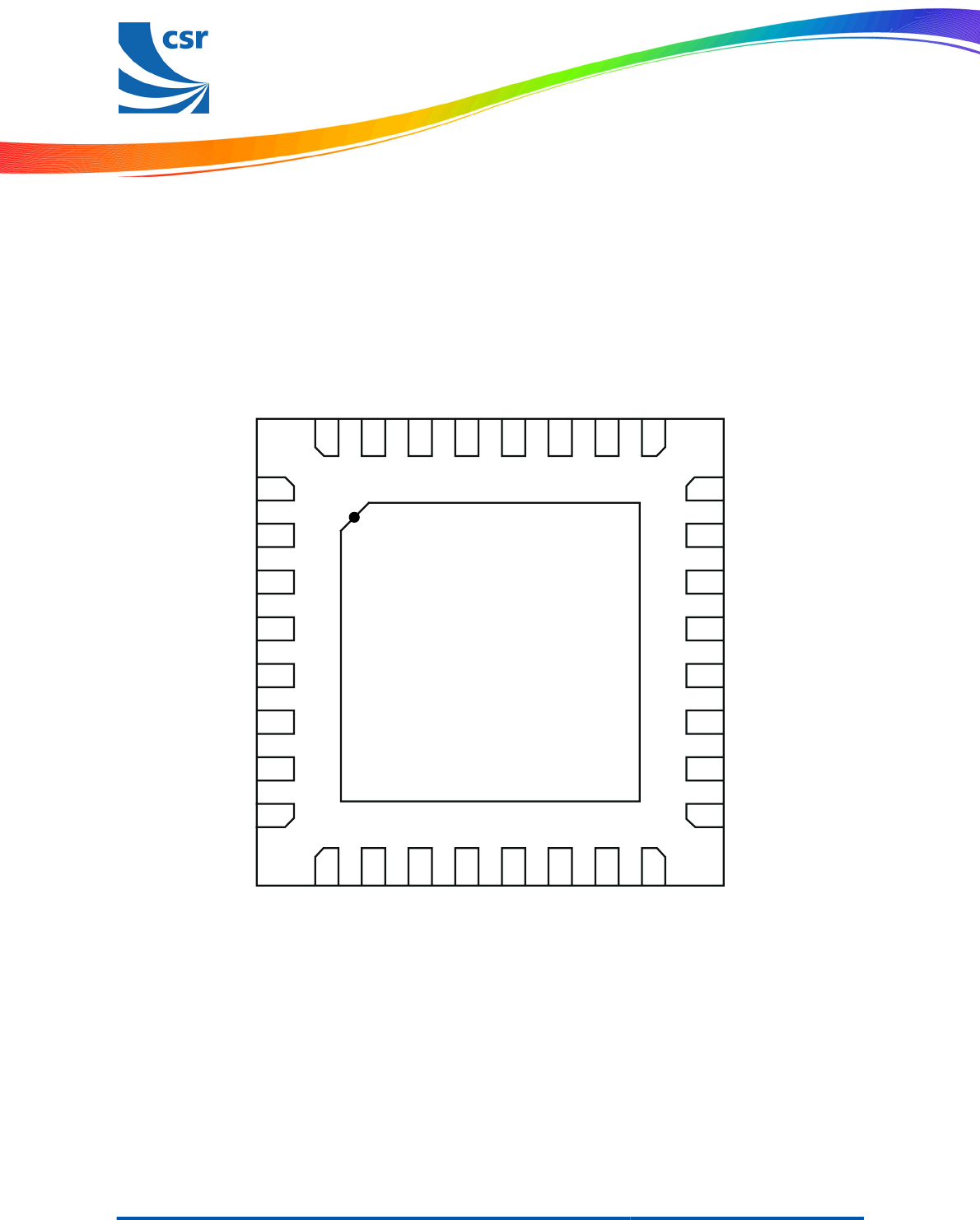
1.1 Pinout Diagram
G-TW-0005350.5.2
Orientation from Top of Device
13
1
2
3
4
5
6
7
8
9 101112 141516
17
18
19
20
21
22
23
24
2526272829303132
Figure 1.1: Pinout Diagram
Production Information
© Cambridge Silicon Radio Limited 2012
This material is subject to CSR's non-disclosure agreement
Page 10 of 42
CS-231985-DSP3
www.csr.com
CSR1010 QFN Data Sheet
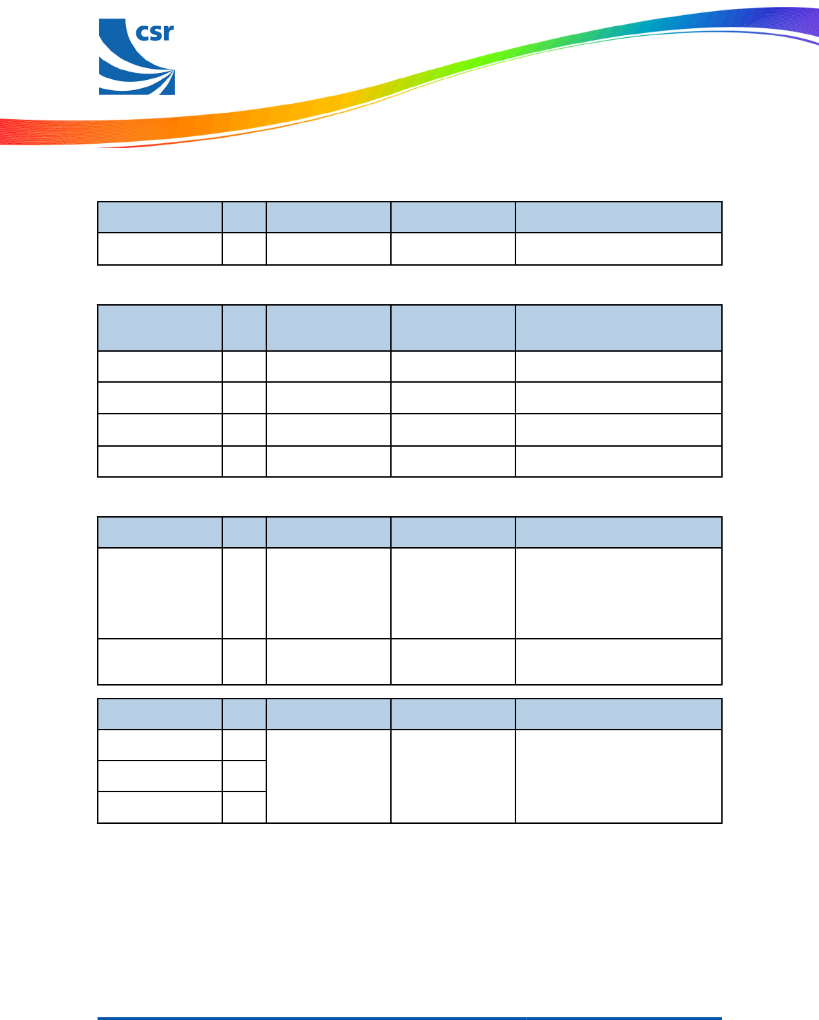
1.2 Device Terminal Functions
Radio Lead Pad Type Supply Domain Description
RF 7RF VDD_RADIO
(a) Bluetooth transmitter / receiver.
(a)
The VDD_RADIO domain is generated from VDD_REG_IN, see Figure 6.1.
Synthesiser and
Oscillator Lead Pad Type Supply Domain Description
XTAL_32K_OUT 2Analogue VDD_BAT Drive for sleep clock crystal.
XTAL_32K_IN 3Analogue VDD_BAT 32.768kHz sleep clock input.
XTAL_16M_OUT 9Analogue VDD_ANA(b) Drive for crystal.
XTAL_16M_IN 10 Analogue VDD_ANA Reference clock input.
(b)
The VDD_ANA domain is generated from VDD_REG_IN, see Figure 6.1.
I²C Interface Lead Pad Type Supply Domain Description
I2C_SDA 29
Bidirectional, tristate,
with weak internal
pull-up
VDD_PADS
I²C data input / output or SPI serial
flash data output (SF_DOUT). If
connecting to SPI serial flash,
connect this pin to SO on the serial
flash. See Section 5.3.
I2C_SCL 28 Input with weak
internal pull-up VDD_PADS I²C clock or SPI serial flash clock
output (SF_CLK), see Section 5.3.
PIO Port Lead Pad Type Supply Domain Description
PIO[11] 25 Bidirectional with
programmable
strength internal pull-
up/down
VDD_PADS Programmable I/O line.
PIO[10] 24
PIO[9] 23
Production Information
© Cambridge Silicon Radio Limited 2012
This material is subject to CSR's non-disclosure agreement
Page 11 of 42
CS-231985-DSP3
www.csr.com
CSR1010 QFN Data Sheet
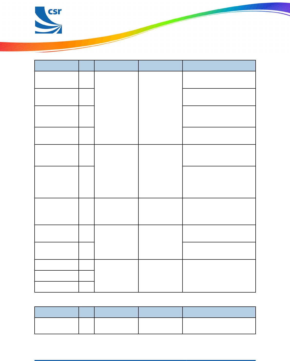
PIO Port Lead Pad Type Supply Domain Description
PIO[8] /
DEBUG_MISO 22
Bidirectional with
programmable
strength internal pull-
up/down
VDD_PADS
Programmable I/O line or debug SPI
MISO selected by SPI_PIO#.
PIO[7] /
DEBUG_MOSI 20 Programmable I/O line or debug SPI
MOSI selected by SPI_PIO#.
PIO[6] /
DEBUG_CS# 19
Programmable I/O line or debug SPI
chip select (CS#) selected by
SPI_PIO#.
PIO[5] /
DEBUG_CLK 18 Programmable I/O line or debug SPI
CLK selected by SPI_PIO#.
PIO[4] /
SF_CS# 17
Bidirectional with
programmable
strength internal pull-
up/down
VDD_PADS
Programmable I/O line or SPI serial
flash chip select (SF_CS#), see
Section 5.3.
PIO[3] /
SF_DIN 16
Programmable I/O line or SPI serial
flash data (SF_DIN) input. If
connecting to SPI serial flash, this
pin connects to SI on the serial flash.
See Section 5.3.
PIO[2] 27
Bidirectional with
programmable
strength internal pull-
up/down
VDD_PADS Programmable I/O line or I²C power.
PIO[1] /
UART_RX 15 Bidirectional with
programmable
strength internal pull-
up/down
VDD_PADS
Programmable I/O line or UART RX.
PIO[0] /
UART_TX 14 Programmable I/O line or UART TX.
AIO[2] 11
Bidirectional
analogue VDD_AUX(c) Analogue programmable I/O line.AIO[1] 12
AIO[0] 13
(c)
The VDD_AUX domain is generated from VDD_REG_IN, see Figure 6.1.
Test and Debug Lead Pad Type Supply Domain Description
SPI_PIO# 26 Input with strong
internal pull-down VDD_PADS Selects SPI debug on PIO[8:5].
Production Information
© Cambridge Silicon Radio Limited 2012
This material is subject to CSR's non-disclosure agreement
Page 12 of 42
CS-231985-DSP3
www.csr.com
CSR1010 QFN Data Sheet
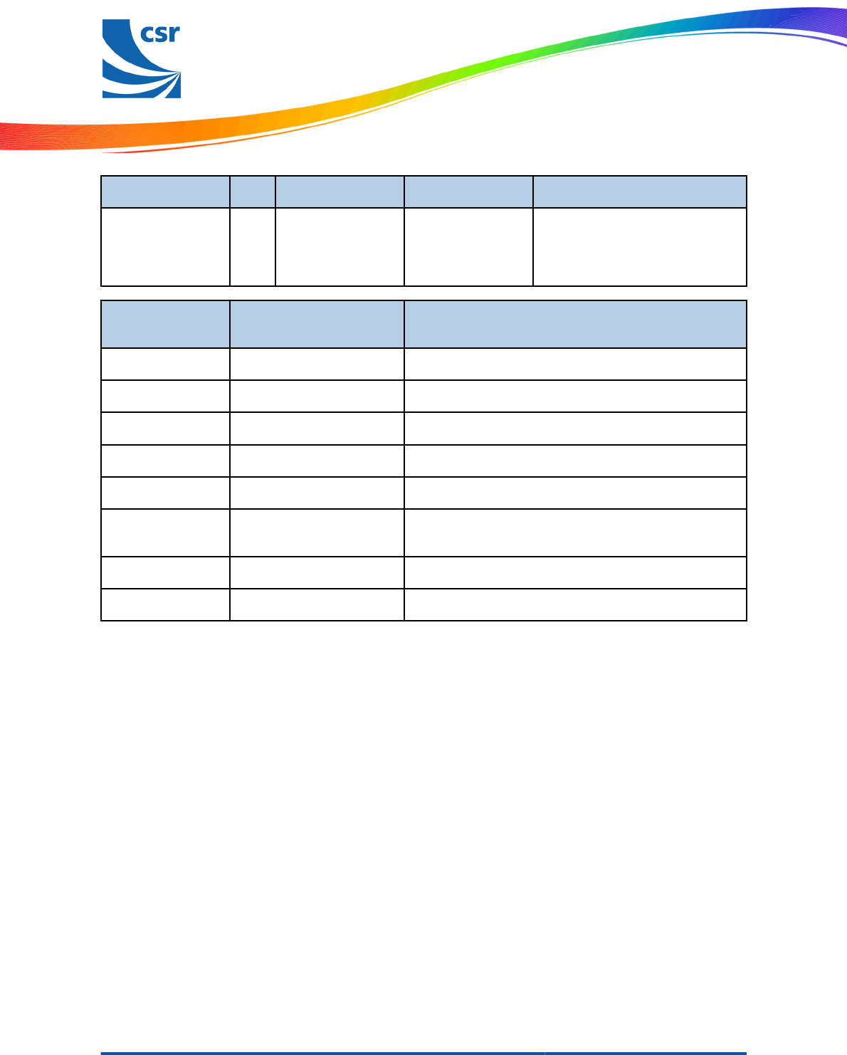
Wake-up Lead Pad Type Supply Domain Description
WAKE 4
Input has no internal
pull-up or pull-down,
use external pull-
down.
VDD_BAT Input to wake CSR1010 QFN from
hibernate or dormant.
Power Supplies and
Control Lead Description
VDD_BAT 1Battery input and regulator enable (active high).
VDD_BAT_SMPS 32 Input to high-voltage switch-mode regulator.
SMPS_LX 31 High-voltage switch-mode regulator output.
VDD_CORE 5, 30 Positive supply for digital domain.
VDD_PADS 21 Positive supply for all digital I/O ports PIO[11:0].
VDD_REG_IN 6Positive supply for Bluetooth radio and digital linear
regulator.
VDD_XTAL 8Decouple with 470nF capacitor to ground.
VSS Exposed pad Ground connections.
Production Information
© Cambridge Silicon Radio Limited 2012
This material is subject to CSR's non-disclosure agreement
Page 13 of 42
CS-231985-DSP3
www.csr.com
CSR1010 QFN Data Sheet
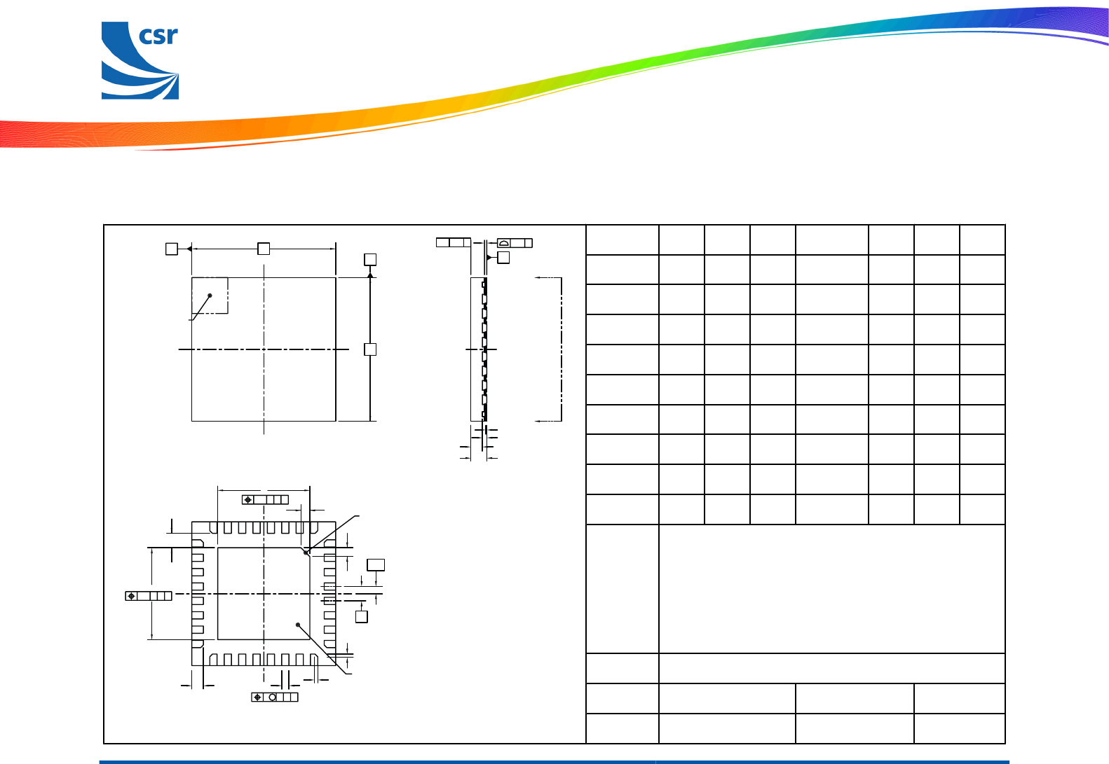
1.3 Package Dimensions
G-TW-0005351.4.3
K
g
A
C
B
g
A
C
B
32X L
17
16
24
25 32
J
PIN 1 ID
1
8
Exposed Die
Attach Pad
9
32X b
d
A
C
B
M
Bottom View
View M-M
e
e / 2
PIN 1 Corner
Top Vie w
32
1
D
B
E
AcC
h
C
//
C
Seating Plane
M
M
P
S
S
R
R
A
A1
A2
A3
Dimension Min Typ Max Dimension Min Typ Max
A0.50 0.55 0.60 e - 0.5 -
A1 00.035 0.05 g - 0.1 -
A2 -0.4 0.425 h - 0.1 -
A3 -0.152 - J 3.1 3.2 3.3
b0.20 0.25 0.30 K3.1 3.2 3.3
c - 0.08 - L 0.35 0.40 0.45
D4.9 5.0 5.1 P0.3 - -
d - 0.10 - R - 0.093 -
E4.9 5.0 5.1 S - 0.3 -
Notes
1.
Coplanarity applies to leads, corner leads and die attach pad.
Description 32-lead Quad-flat No-lead Package
Size 5 x 5 x 0.6mm JEDEC MO-220
Pitch 0.5 Units mm
Production Information
© Cambridge Silicon Radio Limited 2012
This material is subject to CSR's non-disclosure agreement
Page 14 of 42
CS-231985-DSP3
www.csr.com
CSR1010 QFN
Data Sheet

1.4 PCB Design and Assembly Considerations
This section lists recommendations to achieve maximum board-level reliability of the 5 x 5 x 0.6mm QFN 32-lead
package:
■
NSMD lands (lands smaller than the solder mask aperture) are preferred, because of the greater accuracy
of the metal definition process compared to the solder mask process. With solder mask defined pads, the
overlap of the solder mask on the land creates a step in the solder at the land interface, which can cause
stress concentration and act as a point for crack initiation.
■
CSR recommends that the PCB land pattern is in accordance with IPC standard IPC-7351.
■
Solder paste must be used during the assembly process.
1.5 Typical Solder Reflow Profile
See
Typical Solder Reflow Profile for Lead-free Devices
for information.
Production Information
© Cambridge Silicon Radio Limited 2012
This material is subject to CSR's non-disclosure agreement
Page 15 of 42
CS-231985-DSP3
www.csr.com
CSR1010 QFN
Data Sheet

2 Bluetooth Modem
2.1 RF Ports
CSR1010 QFN contains an integrated balun which provides a single-ended RF TX / RX port pin. No matching
components are needed as the receive mode impedance is 50Ω and the transmitter has been optimised to deliver
power in to a 50Ω load.
2.2 RF Receiver
The receiver features a near-zero IF architecture that allows the channel filters to be integrated onto the die. Sufficient
out-of-band blocking specification at the LNA input allows the receiver to be used in close proximity to GSM and
W‑CDMA cellular phone transmitters without being significantly desensitised.
An ADC digitises the IF received signal.
2.2.1 Low Noise Amplifier
The LNA operates in differential mode and takes its input from the balanced port of the integrated balun.
2.2.2 RSSI Analogue to Digital Converter
The ADC samples the RSSI voltage on a packet-by-packet basis and implements a fast AGC. The front-end LNA
gain is changed according to the measured RSSI value, keeping the first mixer input signal within a limited range.
This improves the dynamic range of the receiver, improving performance in interference-limited environments.
2.3 RF Transmitter
2.3.1 IQ Modulator
The transmitter features a direct IQ modulator to minimise frequency drift during a transmit packet, which results in
a controlled modulation index. Digital baseband transmit circuitry provides the required spectral shaping.
2.4 Bluetooth Radio Synthesiser
The Bluetooth radio synthesiser is fully integrated onto the die with no requirement for an external VCO screening
can, varactor tuning diodes, LC resonators or loop filter. The synthesiser is guaranteed to lock in sufficient time
across the guaranteed temperature range to meet the Bluetooth v4.0 specification.
2.5 Baseband
2.5.1 Physical Layer Hardware Engine
Dedicated logic performs:
■
Cyclic redundancy check
■
Encryption
■
Data whitening
■
Access code correlation
The hardware supports all optional and mandatory features of Bluetooth v4.0 specification.
Production Information
© Cambridge Silicon Radio Limited 2012
This material is subject to CSR's non-disclosure agreement
Page 16 of 42
CS-231985-DSP3
www.csr.com
CSR1010 QFN
Data Sheet
3Clock Generation
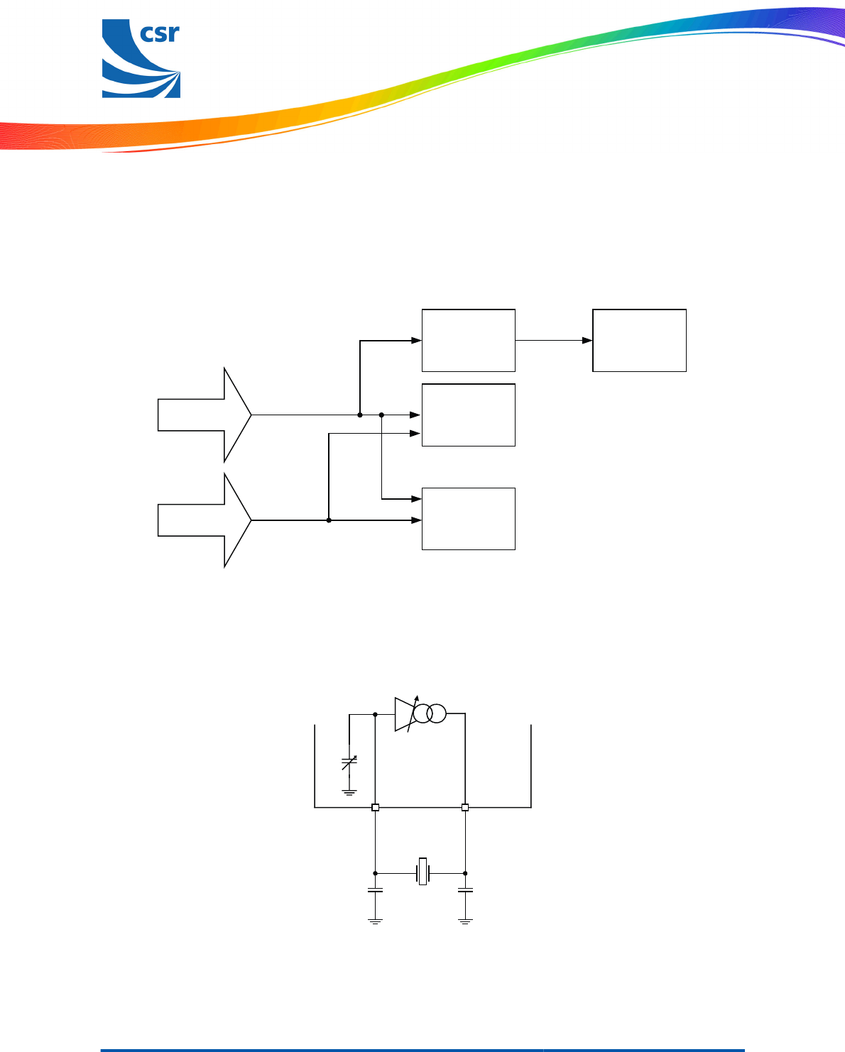
The Bluetooth reference clock for the system is generated from an external 16MHz clock source, see Figure 3.1. All
the CSR1010 QFN internal digital clocks are generated using a phase locked loop, which is locked to the frequency
of either the external reference clock source or a sleep clock frequency of 32.768kHz, see Figure 3.1.
3.1 Clock Architecture
G-TW-0005266.2.2
Fast XTAL Clock
for System
Slow XTAL Clock
for Sleep
Bluetooth PLL
16MHz
32kHz
Core Digits
(16MHz)
Embedded Digits
(32kHz)
Bluetooth LO
(~4.8GHz)
Figure 3.1: Clock Architecture
3.2 Crystal Oscillator: XTAL_16M_IN and XTAL_16M_OUT
CSR1010 QFN contains crystal driver circuits. This operates with an external crystal and capacitors to form a Pierce
oscillator. Figure 3.2 shows the external crystal is connected to pins XTAL_16M_IN and XTAL_16M_OUT.
G-TW-0005348.1.1
-
C
LOAD1
C
LOAD2
XTAL_16M_IN
XTAL_16M_OUT
C
TRIM
Figure 3.2: Crystal Driver Circuit
Production Information
© Cambridge Silicon Radio Limited 2012
This material is subject to CSR's non-disclosure agreement
Page 17 of 42
CS-231985-DSP3
www.csr.com
CSR1010 QFN
Data Sheet
Note:
C
TRIM
is the internal trimmable capacitance in Table 3.1.
C
LOAD1
and C
LOAD2
in combination with C
TRIM
and any parasitic capacitance provide the load capacitance
required by the crystal.
3.2.1 Crystal Specification
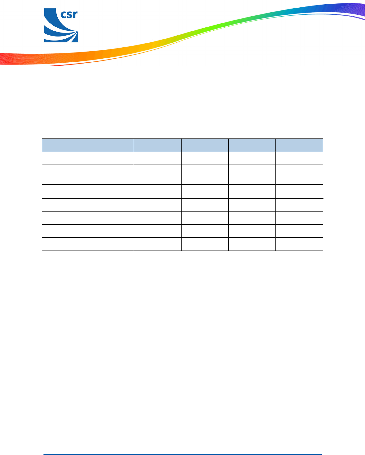
Table 3.1 shows the specification for an external crystal.
Parameter Min Typ Max Unit
Frequency -16 -MHz
Frequency tolerance (without trimming)
(a)
- - ±25 ppm
Frequency trim range
(b)
-±50 -ppm
Drive level - - 100 µW
Equivalent series resistance - - 60 Ω
Load capacitance - 9 - pF
Pullability 10 - - ppm/pF
Table 3.1: Crystal Specification
(a)
Use integrated load capacitors to trim initial frequency tolerance in production or to trim frequency over temperature, increasing the allowable
frequency tolerance.
(b)
Frequency trim range is dependent on crystal load capacitor values and crystal pullability.
3.2.2 Frequency Trim
CSR1010 QFN contains variable integrated capacitors to allow for fine-tuning of the crystal resonant frequency. This
firmware-programmable feature allows accurate trimming of crystals on a per-device basis on the production line.
The resulting trim value is stored in non-volatile memory.
Production Information
© Cambridge Silicon Radio Limited 2012
This material is subject to CSR's non-disclosure agreement
Page 18 of 42
CS-231985-DSP3
www.csr.com
CSR1010 QFN
Data Sheet
3.3 Sleep Clock
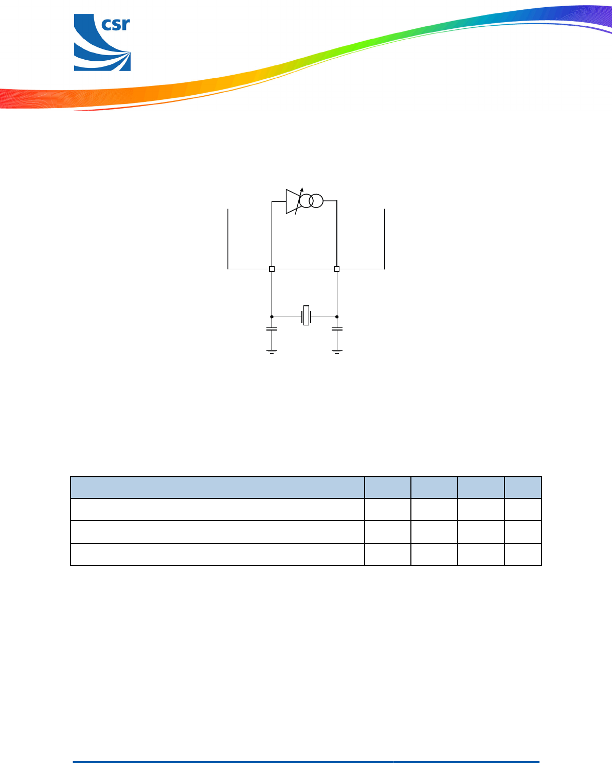
The sleep clock is an externally provided 32.768kHz clock that is used during deep sleep and in other low-power
modes. Figure 3.3 shows the sleep clock crystal driver circuit.
G-TW-0005349.2.2
-
C
LOAD1
C
LOAD2
XTAL_32K_IN
XTAL_32K_OUT
Figure 3.3: Sleep Clock Crystal Driver Circuit
Note:
C
LOAD1
and C
LOAD2
in combination with any parasitic capacitance provide the load capacitance required by the
crystal.
3.3.1 Crystal Specification
Table 3.2 shows the requirements for the sleep clock.
Sleep Clock Min Typ Max Units
Frequency 30 32.768 35 kHz
Frequency tolerance
(a)
(b)
- - 250 ±ppm
Duty cycle 30:70 50:50 70:30 %
Table 3.2: Sleep Clock Specification
(a)
The frequency of the slow clock is periodically calibrated against the system clock. As a result the rate of change of the frequency is more
important than the maximum deviation. To meet the accuracy requirements the frequency should not drift due to temperature or other effects
by more than 80ppm in any 5 minute period.
(b)
CSR1010 QFN can correct for ±1% by using the fast clock to calibrate the slow clock.
Production Information
© Cambridge Silicon Radio Limited 2012
This material is subject to CSR's non-disclosure agreement
Page 19 of 42
CS-231985-DSP3
www.csr.com
CSR1010 QFN
Data Sheet
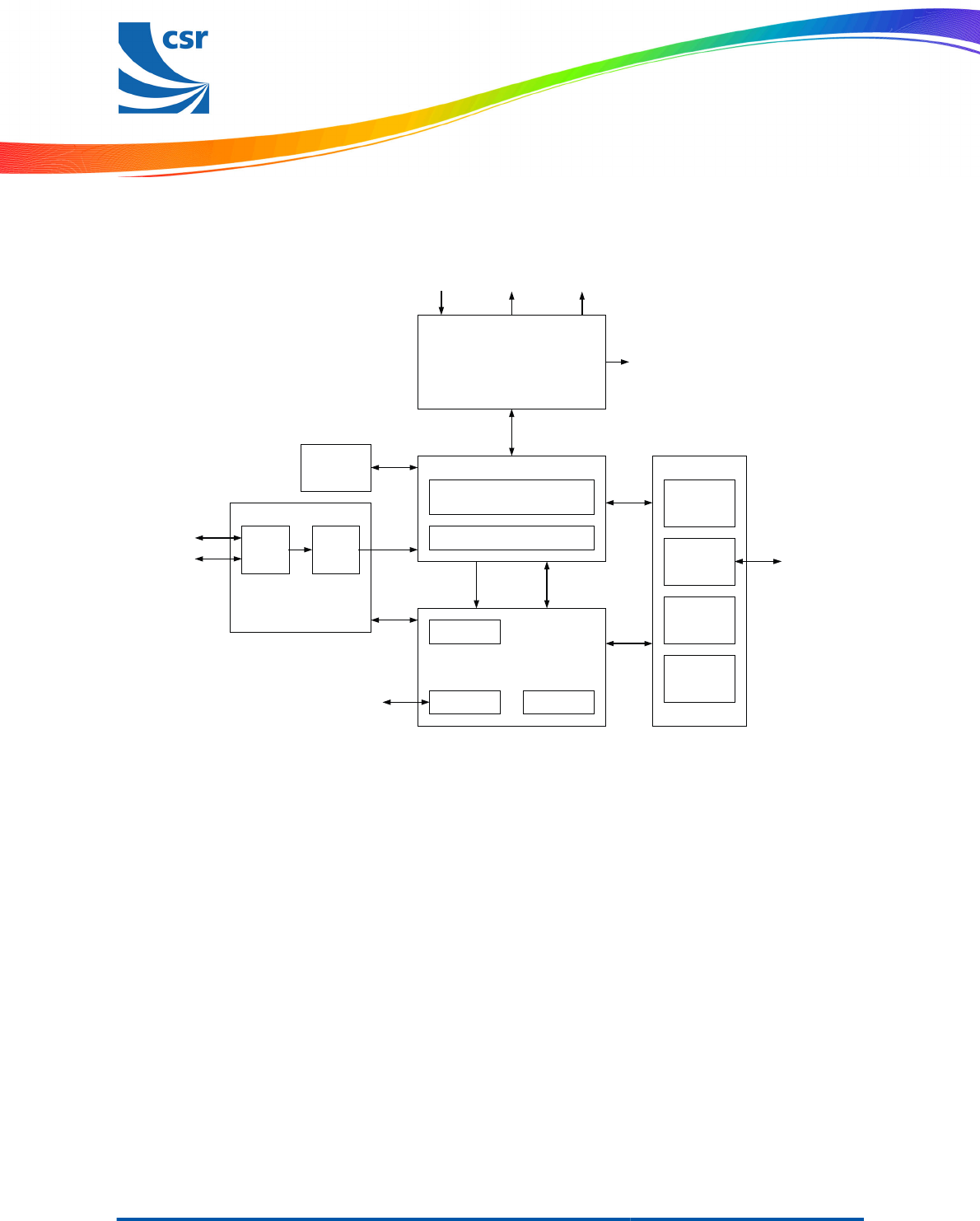
4 Microcontroller, Memory and Baseband Logic
G-TW-0005354.3.2
I2C / Serial Flash
Bluetooth low energy Modem
and LC
RAM Arbiter
RAM
MCU
I2C /
Serial
Flash
I/O
UART
PIO and
LED PWM
AES-CCS and
AES
Encryption
AUX / CLK /
PSU Control
Interrupt
DMA
ADCs DACs
I/O
Control Logic
Memory Protection
Wake-ups
RAM Interface
(Buffers, LUTs, Tables and State)
Bluetooth and
Auxiliary Analogue
Control
PIOs
Debug
I2C EEPROM
Debug Timer
Code Data
Serial Flash
Figure 4.1: Baseband Digits Block Diagram
4.1 System RAM
64KB of integrated RAM supports the RISC MCU and is shared between the ring buffers used to hold data for each
active connection and the general-purpose memory required by the Bluetooth stack.
4.2 Internal ROM
CSR1010 QFN has 64KB of internal ROM. This memory is provided for system firmware implementation. If the
internal ROM holds valid program code, on boot-up, this is copied into the program RAM.
4.3 Microcontroller
The MCU, interrupt controller and event timer run the Bluetooth software stack and control the Bluetooth radio and
external interfaces. A 16-bit RISC microcontroller is used for low power consumption and efficient use of memory.
4.4 Programmable I/O Ports, PIO and AIO
12 lines of programmable bidirectional I/O are provided. They are all powered from VDD_PADS.
PIO lines are software-configurable as weak pull-up, weak pull-down, strong pull-up or strong pull-down.
Note:
At reset all PIO lines are inputs with weak pull-downs.
Production Information
© Cambridge Silicon Radio Limited 2012
This material is subject to CSR's non-disclosure agreement
Page 20 of 42
CS-231985-DSP3
www.csr.com
CSR1010 QFN
Data Sheet

Any of the PIO lines can be configured as interrupt request lines or to wake the IC from deep sleep mode. Table
4.1 lists the options for waking the IC from the sleep modes.
Sleep Mode Wake-up Options
Dormant Can only be woken by the WAKE pin.
Hibernate Can be woken by the WAKE pin or by the watchdog timer.
Deep Sleep Can be woken by any PIO configured to wake the IC.
Table 4.1: Wake Options for Sleep Modes
The CSR1010 QFN supports alternative functions on the PIO lines:
■
SPI interface, see Section 1.2 and Section 5.4
■
UART, see Section 1.2 and Section 5.1.1
■
LED flasher / PWM module, see Section 4.5
Note:
CSR cannot guarantee that the PIO assignments remain as described. Implementation of the PIO lines is
firmware build-specific, for more information see the relevant software release note.
CSR1010 QFN has 3 general-purpose analogue interface pins, AIO[2:0].
4.5 LED Flasher / PWM Module
CSR1010 QFN contains a LED flasher / PWM module that works in sleep modes.
These functions are controlled by the on-chip firmware.
Production Information
© Cambridge Silicon Radio Limited 2012
This material is subject to CSR's non-disclosure agreement
Page 21 of 42
CS-231985-DSP3
www.csr.com
CSR1010 QFN
Data Sheet
5 Serial Interfaces
5.1 Application Interface
5.1.1 UART Interface
The CSR1010 QFN UART interface provides a simple mechanism for communicating with other serial devices using
the RS232 protocol.
2 signals implement the UART function, UART_TX and UART_RX. When CSR1010 QFN is connected to another
digital device, UART_RX and UART_TX transfer data between the 2 devices.
UART configuration parameters, e.g. baud rate and data format, are set using CSR1010 QFN firmware.
When selected in firmware PIO[0] is assigned to a UART_TX output and PIO[1] is assigned to a UART_RX input,
see Section 1.2.
The UART CTS and RTS signals can be assigned to any PIO pin by the on-chip firmware.
Note:
To communicate with the UART at its maximum data rate using a standard PC, the PC requires an accelerated
serial port adapter card.
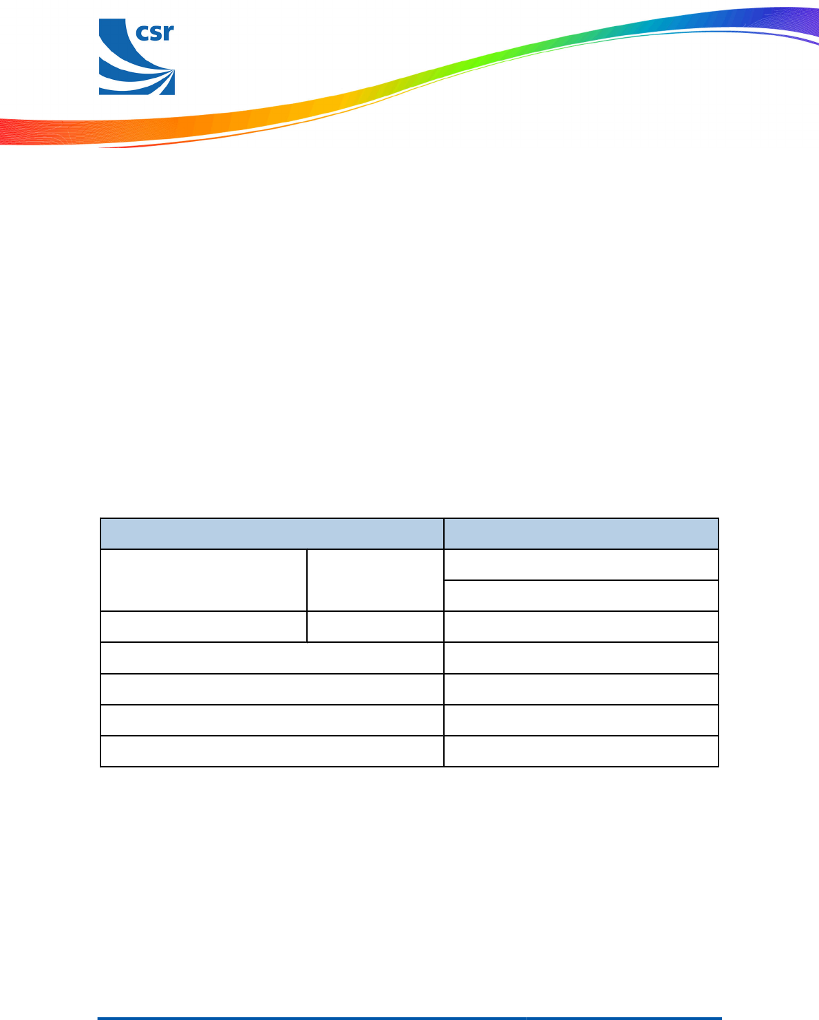
Table 5.1 shows the possible UART settings for the CSR1010 QFN.
Parameter Possible Values
Baud rate Minimum
1200 baud (≤2%Error)
9600 baud (≤1%Error)
Maximum 2Mbaud (≤1%Error)
Flow control CTS / RTS
Parity None, Odd or Even
Number of stop bits 1 or 2
Bits per byte 8
Table 5.1: Possible UART Settings
5.1.1.1 UART Configuration While in Deep Sleep
The maximum baud rate is 9600 baud during deep sleep.
5.2 I²C Interface
The I²C interface communicates to EEPROM, external peripherals or sensors. An external EEPROM connection
can hold the program code externally to the CSR1010 QFN.
Production Information
© Cambridge Silicon Radio Limited 2012
This material is subject to CSR's non-disclosure agreement
Page 22 of 42
CS-231985-DSP3
www.csr.com
CSR1010 QFN
Data Sheet
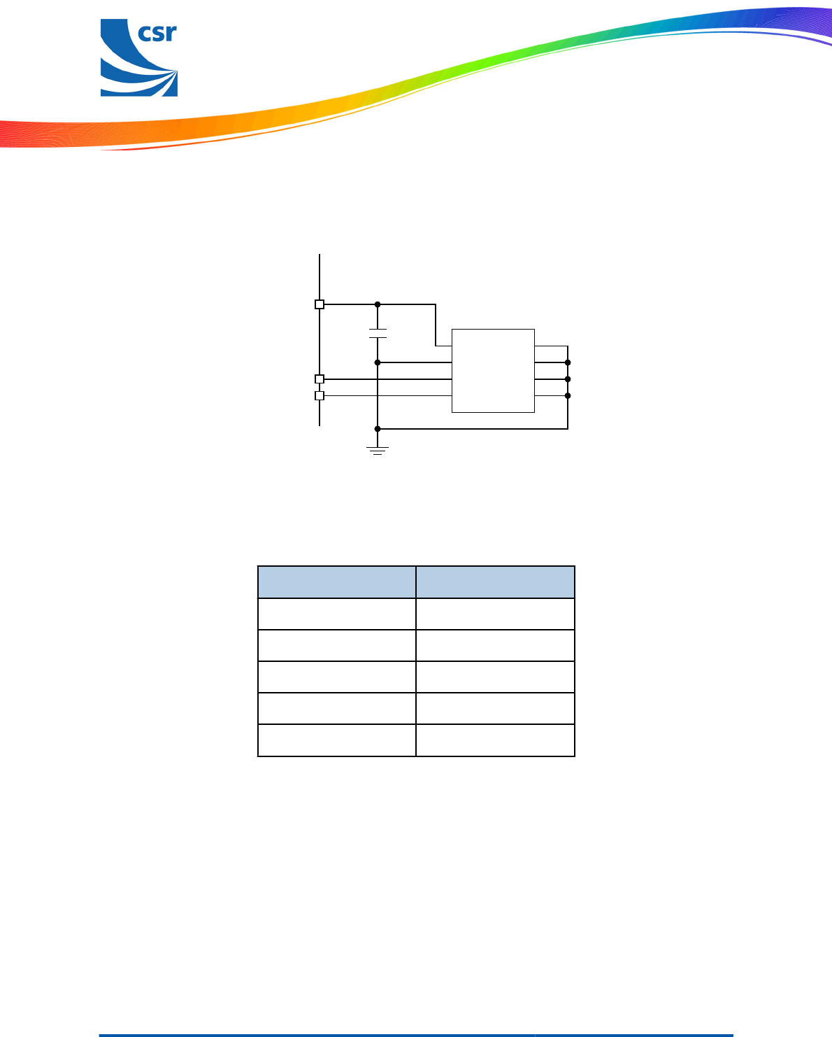
Figure 5.1 shows an example of an EEPROM connected to the I²C interface where I2C_SCL, I2C_SDA and PIO[2]
are connected to the external EEPROM. The PIO[2] pin supplies the power to the EEPROM supply pin, e.g. VDD.
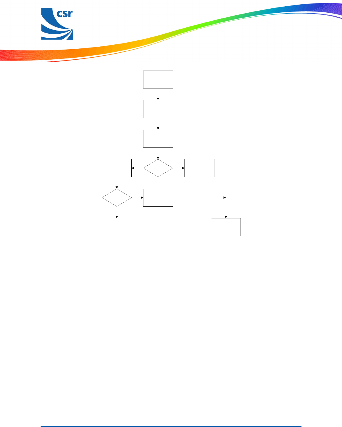
At boot-up, if there is no valid ROM image in the CSR1010 QFN ROM area the CSR1010 QFN tries to boot from
the I²C interface, see Figure 5.2. This involves reading the code from the external EEPROM and loading it into the
internal CSR1010 QFN RAM.
G-TW-0005553.1.1
VDD
WP
SCL
SDA
A0
A1
A2
VSS
I2C_SCL
I2C_SDA
PIO[2]
1
2
3
45
6
7
8
24AA512
Figure 5.1: Example of an I²C Interface EEPROM Connection
5.3 SPI Master Interface
The SPI master memory interface in the CSR1010 QFN is overlaid on the I²C interface and uses a further 3 PIOs
for the extra pins, see Table 5.2.
SPI Flash Interface Pin
Flash_VDD PIO[2]
SF_DIN PIO[3]
SF_CS# PIO[4]
SF_CLK I2C_SCL
SF_DOUT I2C_SDA
Table 5.2: SPI Master Serial Flash Memory Interface
Note:
If an application using CSR1010 QFN is designed to boot from SPI serial flash, it is possible for the firmware to
map the I²C interface to alternative PIOs.
The boot-up sequence for CSR1010 QFN is controlled by hardware and firmware. Figure 5.2 shows the sequence
of loading RAM with content from RAM, EEPROM and SPI serial flash.
Production Information
© Cambridge Silicon Radio Limited 2012
This material is subject to CSR's non-disclosure agreement
Page 23 of 42
CS-231985-DSP3
www.csr.com
CSR1010 QFN
Data Sheet
G-TW-0005552.2.2
Device Starts
Hardware Copies
Content of ROM to RAM
Hardware Checks I 2C
Interface (Default Pins )
Presence of
EEPROM Device
Hardware Checks SPI
Interface ( D efault Pins )
Presence of SPI
Serial Flash D evice
Star t M CU Executing
from RAM
Copy Content of SPI
Ser i al Flash to RAM
Copy Content of
EEPROM to RAM
YesNo
Yes
No
Figure 5.2: Memory Boot-up Sequence
5.4 Programming and Debug Interface
Important Note:
The CSR1010 QFN debug SPI interface is available in SPI slave mode to enable an external MCU to program
and control the CSR1010 QFN, generally via libraries or tools supplied by CSR. The protocol of this interface
is proprietary. The 4 SPI debug lines directly support this function.
The SPI programs, configures and debugs the CSR1010 QFN. It is required in production. Ensure the 4 SPI
signals are brought out to either test points or a header.
Take SPI_PIO#_SEL high to enable the SPI debug feature on PIO[8:5].
CSR1010 QFN uses a 16-bit data and 16-bit address programming and debug interface. Transactions occur when
the internal processor is running or is stopped.
Data is written or read one word at a time, or the auto-increment feature is available for block access.
5.4.1 Instruction Cycle
The CSR1010 QFN is the slave and receives commands on DEBUG_MOSI and outputs data on DEBUG_MISO.
Table 5.3 shows the instruction cycle for a SPI transaction.
Production Information
© Cambridge Silicon Radio Limited 2012
This material is subject to CSR's non-disclosure agreement
Page 24 of 42
CS-231985-DSP3
www.csr.com
CSR1010 QFN
Data Sheet
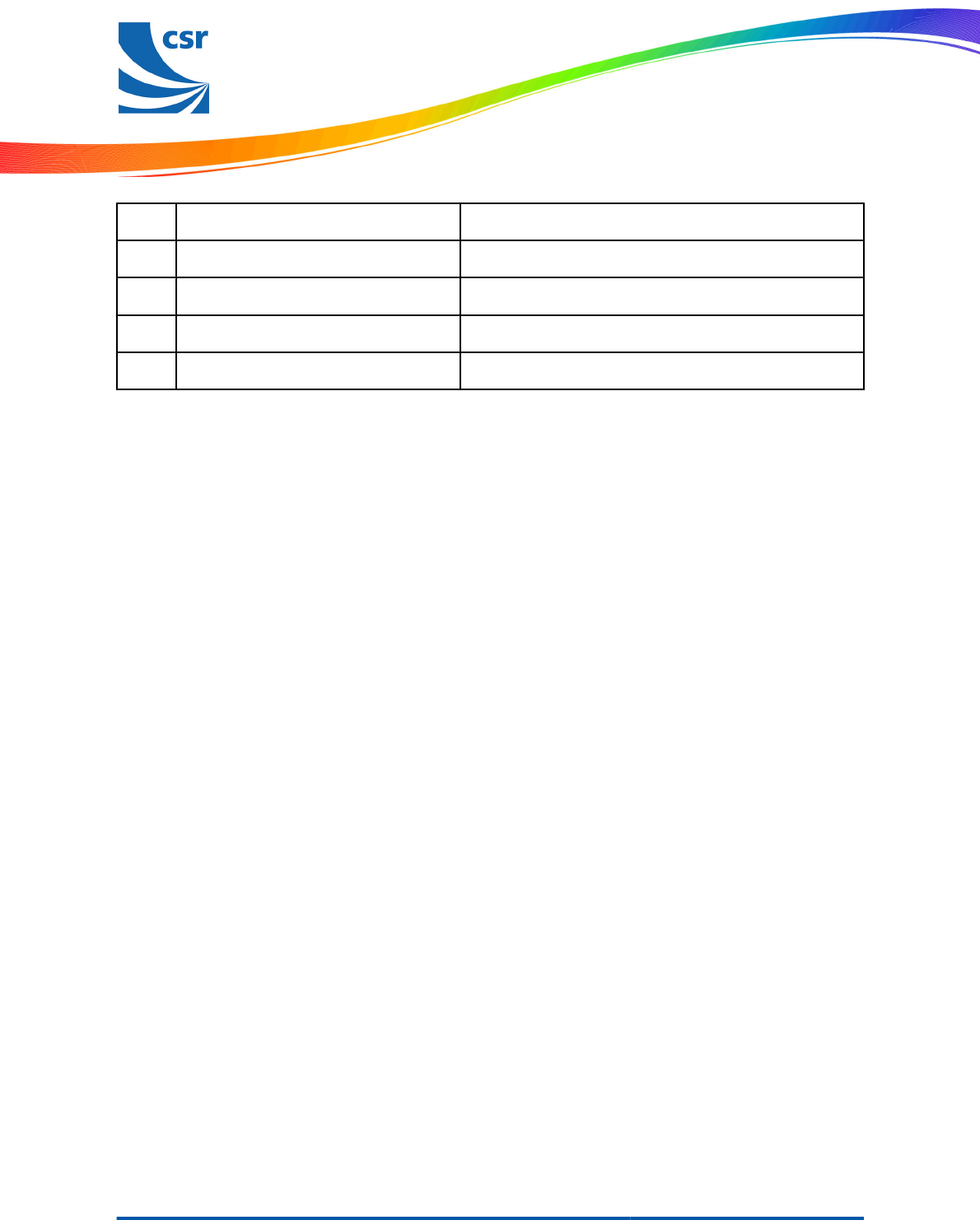
1Reset the SPI interface Hold DEBUG_CS# high for 2 DEBUG_CLK cycles
2Write the command word Take DEBUG_CS# low and clock in the 8-bit command
3Write the address Clock in the 16-bit address word
4Write or read data words Clock in or out 16-bit data word(s)
5Termination Take DEBUG_CS# high
Table 5.3: Instruction Cycle for a SPI Transaction
With the exception of reset, DEBUG_CS# must be held low during the transaction. Data on DEBUG_MOSI is clocked
into the CSR1010 QFN on the rising edge of the clock line DEBUG_CLK. When reading, CSR1010 QFN replies to
the master on DEBUG_MISO with the data changing on the falling edge of the DEBUG_CLK. The master provides
the clock on DEBUG_CLK. The transaction is terminated by taking DEBUG_CS# high.
The auto increment operation on the CSR1010 QFN cuts down on the overhead of sending a command word and
the address of a register for each read or write, especially when large amounts of data are to be transferred. The
auto increment offers increased data transfer efficiency on the CSR1010 QFN. To invoke auto increment,
DEBUG_CS# is kept low, which auto increments the address, while providing an extra 16 clock cycles for each extra
word written or read.
5.4.2 Multi-slave Operation
Do not connect the CSR1010 QFN in a multi-slave arrangement by simple parallel connection of slave MISO lines.
When CSR1010 QFN is deselected (DEBUG_CS# = 1), the DEBUG_MISO line does not float. Instead,
CSR1010 QFN outputs
0
if the processor is running or
1
if it is stopped.
Production Information
© Cambridge Silicon Radio Limited 2012
This material is subject to CSR's non-disclosure agreement
Page 25 of 42
CS-231985-DSP3
www.csr.com
CSR1010 QFN
Data Sheet
6 Power Control and Regulation
CSR1010 QFN contains 2 regulators:
■
1 switch-mode regulator, which generates the main supply rail from the battery
■
1 low-voltage linear regulator
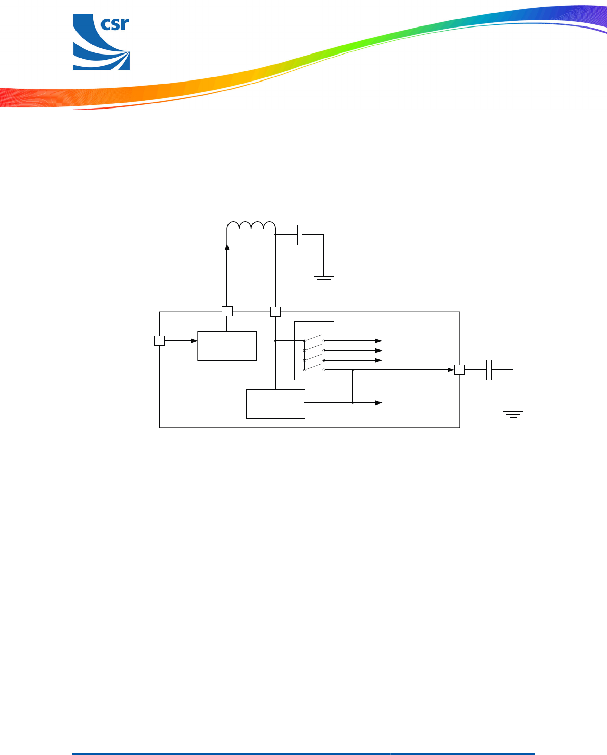
Figure 6.1 shows the configuration for the power control and regulation with the CSR1010 QFN.
G-TW-0005367.4.3
Switch-mode
Regulator
Switch
SMPS_LX
VDD _BAT _SMPS
Low-voltage
VDD_DIG
Linear Regulator
VDD_AUX 1.35 V
VDD_RADIO 1.35 V
VDD_ANA 1.35V
Digits 0.65 /1.20 V
VDD _CORE
VDD_REG_IN
Figure 6.1: Voltage Regulator Configuration
6.1 Switch-mode Regulator
The switch-mode regulator generates the main rail from the battery supply, VDD_BAT_SMPS. The main rail supplies
the lower regulated voltage to a further digital linear regulator and also to the analogue sections of the CSR1010 QFN.
The switch-mode regulator generates typically 1.35V.
6.2 Low-voltage VDD_DIG Linear Regulator
The integrated low-voltage VDD_DIG linear regulator powers the CSR1010 QFN digital circuits. The input voltage
range is 0.65V to 1.35V. It can supply programmable voltages of 0.65V to 1.20V to the digital area of the
CSR1010 QFN. The maximum output current for this regulator is 30mA.
Connect a minimum 470nF low ESR capacitor, e.g. MLC, to the VDD_CORE output pin. Software controls the output
voltage.
Important Note:
This regulator is only for CSR internal use. Section 7 shows CSR's recommended circuit connection.
6.3 Reset
CSR1010 QFN is reset by:
■
Power-on reset
■
Software-configured watchdog timer
Production Information
© Cambridge Silicon Radio Limited 2012
This material is subject to CSR's non-disclosure agreement
Page 26 of 42
CS-231985-DSP3
www.csr.com
CSR1010 QFN
Data Sheet

6.3.1 Digital Pin States on Reset
Table 6.1 shows the pin states of CSR1010 QFN on reset. PU and PD default to weak values unless specified
otherwise.
Pin Name / Group On Reset
I2C_SDA Strong PU
I2C_SCL Strong PU
PIO[11:0] Weak PD
Table 6.1: Pin States on Reset
6.3.2 Power-on Reset
Table 6.2 shows how the power-on reset occurs.
Power-on Reset Typ Unit
Reset release on VDD_DIG rising 1.05
V
Reset assert on VDD_DIG falling 1.00
Reset assert on VDD_DIG falling (Sleep mode) 0.60
Hysteresis 50 mV
Table 6.2: Power-on Reset
Production Information
© Cambridge Silicon Radio Limited 2012
This material is subject to CSR's non-disclosure agreement
Page 27 of 42
CS-231985-DSP3
www.csr.com
CSR1010 QFN
Data Sheet
8 Electrical Characteristics
8.1 Absolute Maximum Ratings
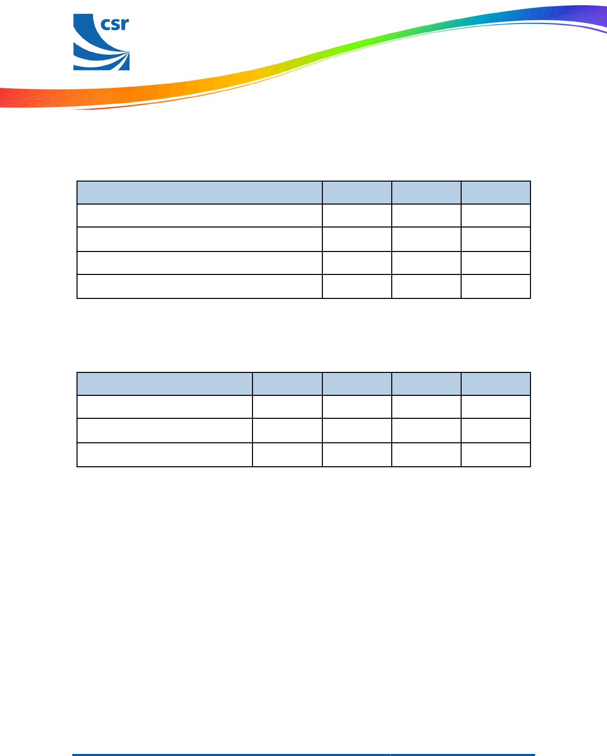
Rating Min Max Unit
Storage temperature -40 85 °C
Battery (VDD_BAT) operation
(a)
1.8 3.6 V
I/O supply voltage -0.4 3.6 V
Other terminal voltages
(b)
VSS - 0.4 VDD + 0.4 V
(a)
CSR1010 QFN is reliable and qualifiable to 4.2V, but there will be minor deviations in performance relative to published performance values
for 1.8V to 3.6V.
(b)
VDD = Terminal Supply Domain
8.2 Recommended Operating Conditions
Operating Condition Min Typ Max Unit
Operating temperature range -30 -85 °C
Battery (VDD_BAT) operation
(a)
1.8 -3.6 V
I/O supply voltage (VDD_PADS)
(b)
1.2 -3.6 V
(a)
CSR1010 QFN is reliable and qualifiable to 4.2V, but there will be minor deviations in performance relative to published performance values
for 1.8V to 3.6V.
(b)
Safe to 4.2V if VDD_BAT = 4.2V.
Production Information
© Cambridge Silicon Radio Limited 2012
This material is subject to CSR's non-disclosure agreement
Page 29 of 42
CS-231985-DSP3
www.csr.com
CSR1010 QFN
Data Sheet
8.3 Input/Output Terminal Characteristics
8.3.1 Switch-mode Regulator
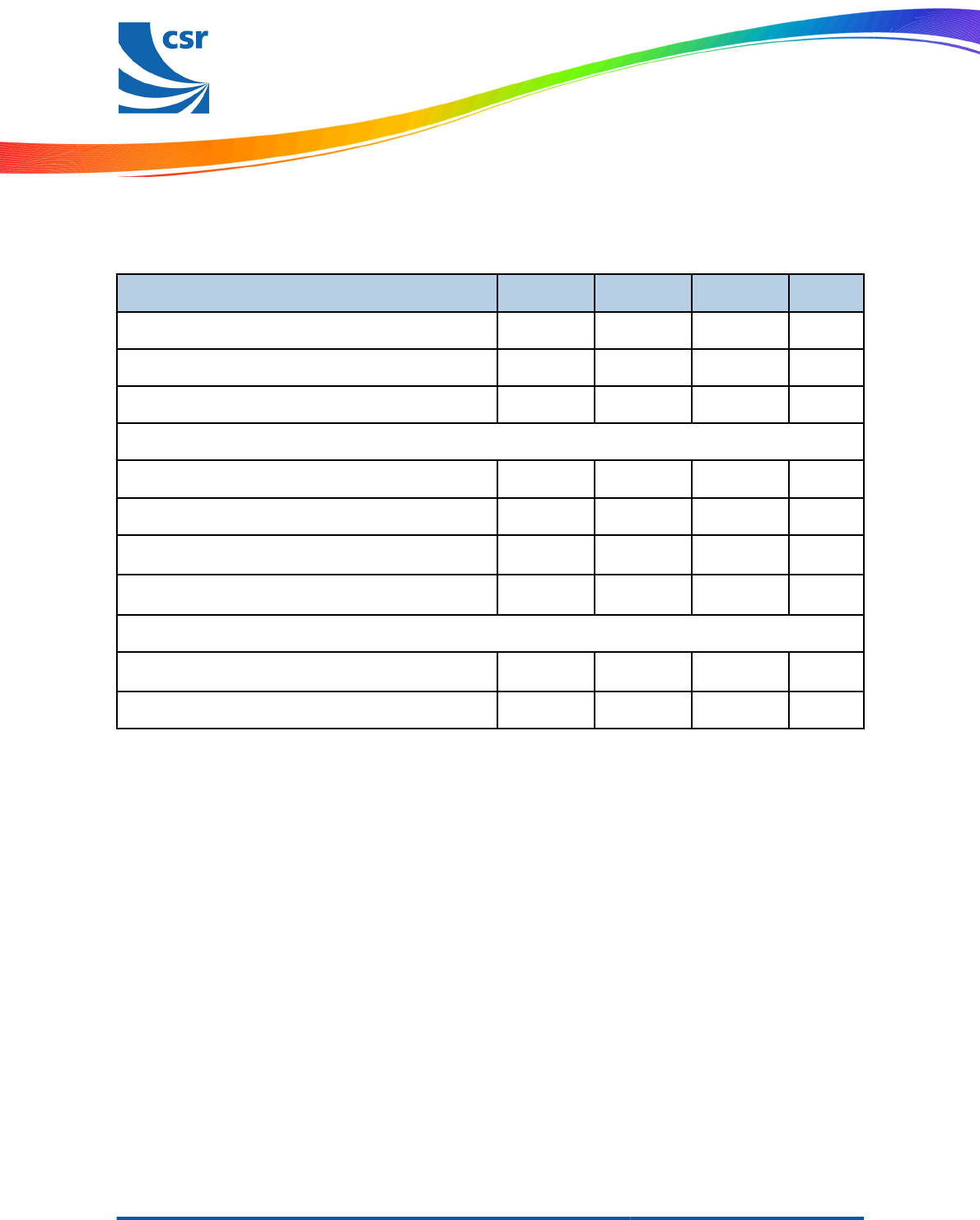
Switch-mode Regulator Min Typ Max Unit
Input voltage 1.8 -3.6 V
Output voltage 0.65 1.35 1.35 V
Temperature coefficient -200 -200 ppm/°C
Normal Operation
Output noise, frequency range 100Hz to 100kHz - - 0.4 mV rms
Settling time, settling to within 10% of final value - - 30 μs
Output current (I
max
)- - 50 mA
Quiescent current (excluding load, I
load
< 1mA) - - 20 µA
Ultra Low-power Mode
Output current (I
max
)- - 100 µA
Quiescent current - - 1 µA
Production Information
© Cambridge Silicon Radio Limited 2012
This material is subject to CSR's non-disclosure agreement
Page 30 of 42
CS-231985-DSP3
www.csr.com
CSR1010 QFN
Data Sheet
8.3.2 Low-voltage Linear Regulator
Normal Operation Min Typ Max Unit
Input voltage 0.65 -1.35 V
Output voltage 0.65 -1.20 V
Important Note:
This regulator is only for CSR internal use. Section 7 shows CSR's recommended circuit connection.
8.3.3 Digital Terminals
Input Voltage Levels Min Typ Max Unit
V
IL
input logic level low -0.4 -0.3 x
VDD_PADS V
V
IH
input logic level high 0.7 x VDD - VDD + 0.4 V
T
r
/T
f
- - 25 ns
Output Voltage Levels Min Typ Max Unit
V
OL
output logic level low, l
OL
= 4.0mA - - 0.4 V
V
OH
output logic level high, l
OH
= -4.0mA 0.75 x VDD - - V
T
r
/T
f
- - 5 ns
Input and Tristate Currents Min Typ Max Unit
With strong pull-up -150 -40 -10 μA
I²C with strong pull-up -250 - - μA
With strong pull-down 10 40 150 μA
With weak pull-up -5.0 -1.0 -0.33 μA
With weak pull-down 0.33 1.0 5.0 μA
C
I
input capacitance 1.0 -5.0 pF
Production Information
© Cambridge Silicon Radio Limited 2012
This material is subject to CSR's non-disclosure agreement
Page 31 of 42
CS-231985-DSP3
www.csr.com
CSR1010 QFN
Data Sheet
8.3.4 AIO
Input Voltage Levels Min Typ Max Unit
Input voltage 0 - VDD_AUX V
8.4 ESD Protection
Apply ESD static handling precautions during manufacturing.
Table 8.1 shows the ESD handling maximum ratings.
Condition Class Max Rating
Human Body Model Contact Discharge per JEDEC EIA/JESD22-A114 22000V (all pins)
Machine Model Contact Discharge per JEDEC EIA/JESD22-A115 200V 200V (all pins)
Charged Device Model Contact Discharge per JEDEC EIA/JESD22-C101III 500V (all pins)
Table 8.1: ESD Handling Ratings
Production Information
© Cambridge Silicon Radio Limited 2012
This material is subject to CSR's non-disclosure agreement
Page 32 of 42
CS-231985-DSP3
www.csr.com
CSR1010 QFN
Data Sheet
9 Current Consumption
Table 9.1 shows CSR1010 QFN total typical current consumption measured at the battery.
Mode Description Total Typical Current at 3V
Dormant All functions are shut down. To wake them up, toggle the
WAKE pin. <600nA
Hibernate VDD_PADS = ON, REFCLK = OFF, SLEEPCLK = ON,
VDD_BAT = ON <1.5µA
Deep sleep
VDD_PADS = ON, REFCLK = OFF, SLEEPCLK = ON,
VDD_BAT = ON, RAM = ON, digital circuits = ON,
SMPS = ON (low-power mode), 1ms wake-up time
<5μA
Idle
VDD_PADS = ON, REFCLK = ON, SLEEPCLK = ON,
VDD_BAT = ON, RAM = ON, digital circuits = ON,
MCU = IDLE, <1μs wake-up time
~1mA
RX / TX active -~16mA @ 3V peak current
Table 9.1: Current Consumption
Production Information
© Cambridge Silicon Radio Limited 2012
This material is subject to CSR's non-disclosure agreement
Page 33 of 42
CS-231985-DSP3
www.csr.com
CSR1010 QFN
Data Sheet

10 CSR Green Semiconductor Products and RoHS Compliance
CSR confirms that CSR Green semiconductor products comply with the following regulatory requirements:
■
Restriction on Hazardous Substances directive guidelines in the EU RoHS Directive 2002/95/EC and RoHS
recast 2011/65/EU
1
from 3 Jan 2013.
■
EU REACH, Regulation (EC) No 1907/2006
1
:
■
List of substances subject to authorisation (Annex XIV)
■
Restrictions on the manufacture, placing on the market and use of certain dangerous substances,
preparations and articles (Annex XVII). This Annex now includes requirements that were contained
within EU Directive, 76/769/EEC. There are many substance restrictions within this Annex, including,
but not limited to, the control of use of Perfluorooctane sulfonates (PFOS).
■
When requested by customers, notification of substances identified on the Candidate List as
Substances of Very High Concern (SVHC)
1
.
■
POP regulation (EC) No 850/2004
1
■
EU Packaging and Packaging Waste, Directive 94/62/EC
1
■
Montreal Protocol on substances that deplete the ozone layer.
■
Conflict minerals, Section 1502, Dodd-Frank Wall Street Reform and Consumer Protection act, which
affects columbite-tantalite (coltan / tantalum), cassiterite (tin), gold, wolframite (tungsten) or their
derivatives. CSR is a fabless semiconductor company: all manufacturing is performed by key suppliers.
CSR have mandated that the suppliers shall not use materials that are sourced from "conflict zone mines"
but understand that this requires accurate data from the EICC programme. CSR shall provide a complete
EICC / GeSI template upon request.
CSR has defined the "CSR Green" standard based on current regulatory and customer requirements including free
from bromine, chlorine and antimony trioxide.
Products and shipment packaging are marked and labelled with applicable environmental marking symbols in
accordance with relevant regulatory requirements.
This identifies the main environmental compliance regulatory restrictions CSR specify. For more information on the
full "CSR Green" standard, contact product.compliance@csr.com.
1
Including applicable amendments to EU law which are published in the EU Official Journal, or SVHC
Candidate List updates published by the European Chemicals Agency (ECHA).
Production Information
© Cambridge Silicon Radio Limited 2012
This material is subject to CSR's non-disclosure agreement
Page 34 of 42
CS-231985-DSP3
www.csr.com
CSR1010 QFN
Data Sheet
11 CSR1010 QFN Software Stack
CSR1010 QFN is supplied with Bluetooth v4.0 specification compliant stack firmware. Figure 11.1 shows that the
CSR1010 QFN software architecture enables the Bluetooth processing and the application program to run on the
internal RISC MCU.
G-TW-0005570.1.1
Device Manager
Generic Attribute
Profile (GATT)
Application
Security
Manager (SM)
Attribute Profile
(ATT)
L2CAP
Link Layer Control
Digital Radio Control
Physical Layer
Software Radio Control
Figure 11.1: Software Architecture
Production Information
© Cambridge Silicon Radio Limited 2012
This material is subject to CSR's non-disclosure agreement
Page 35 of 42
CS-231985-DSP3
www.csr.com
CSR1010 QFN
Data Sheet
12 Tape and Reel Information
For tape and reel packing and labelling see
IC Packing and Labelling Specification
.
12.1 Tape Orientation
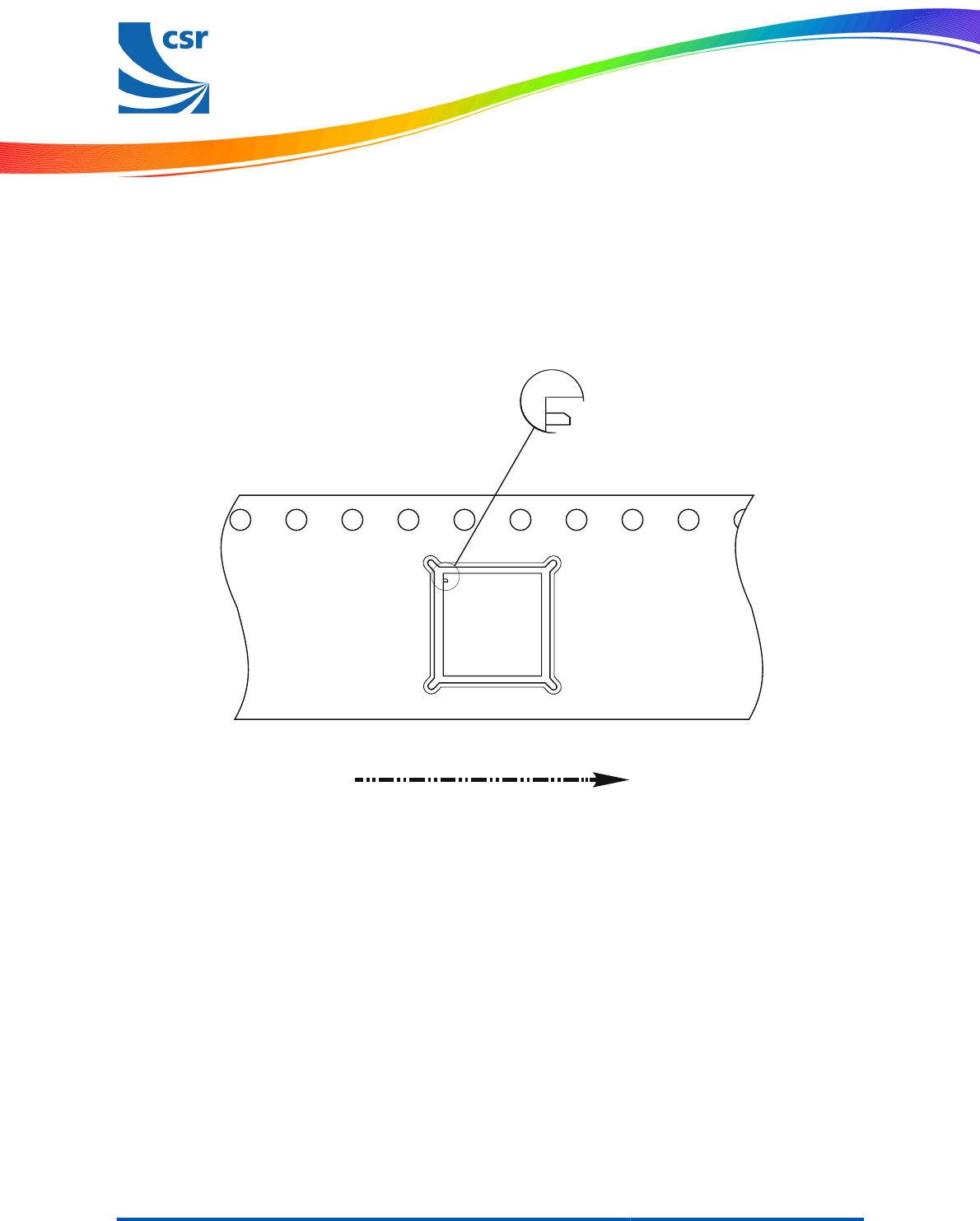
Figure 12.1 shows the CSR1010 QFN packing tape orientation.
G-TW-0002812.2.2
User Direction of Feed
Pin 1
Figure 12.1: Tape Orientation
Production Information
© Cambridge Silicon Radio Limited 2012
This material is subject to CSR's non-disclosure agreement
Page 36 of 42
CS-231985-DSP3
www.csr.com
CSR1010 QFN
Data Sheet
12.2 Tape Dimensions
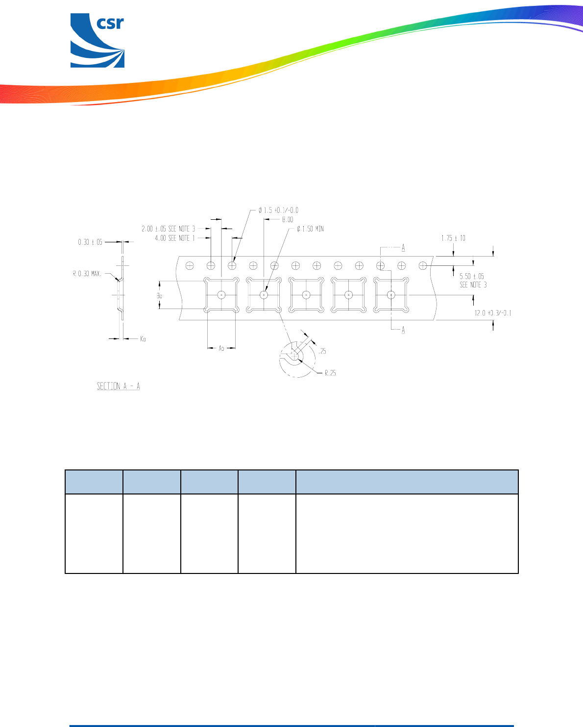
Figure 12.2 shows the dimensions of the tape for the CSR1010 QFN.
G-TW-0005504.1.1
Figure 12.2: Tape Dimensions
A
0
B
0
K
0
Unit Notes
5.25 5.25 0.80 mm
1. 10 sprocket hole pitch cumulative tolerance ±0.2.
2. Camber in compliance with EIA 481.
3. Pocket position relative to sprocket hole measured
as true position of pocket, not pocket hole.
4. A
0
and B
0
are calculated on a plane at a distance
"R" above the bottom of the pocket.
Production Information
© Cambridge Silicon Radio Limited 2012
This material is subject to CSR's non-disclosure agreement
Page 37 of 42
CS-231985-DSP3
www.csr.com
CSR1010 QFN
Data Sheet
12.3 Reel Information
G-TW-0002797.5.2
102.0
2.0
330.0
2.0
W1
(MEASURED AT HUB)
(MEASURED AT HUB)
"A"
ATTENTION
Electrostatic Sensitive Devices
Safe Handling Required
W2
20.2
MIN
2.0 0.5
13.0
+0.5
-0.2
Detail "A"
Detail "B"
6
PS
PS
6
a
(rim height)
88 REF
"b" REF
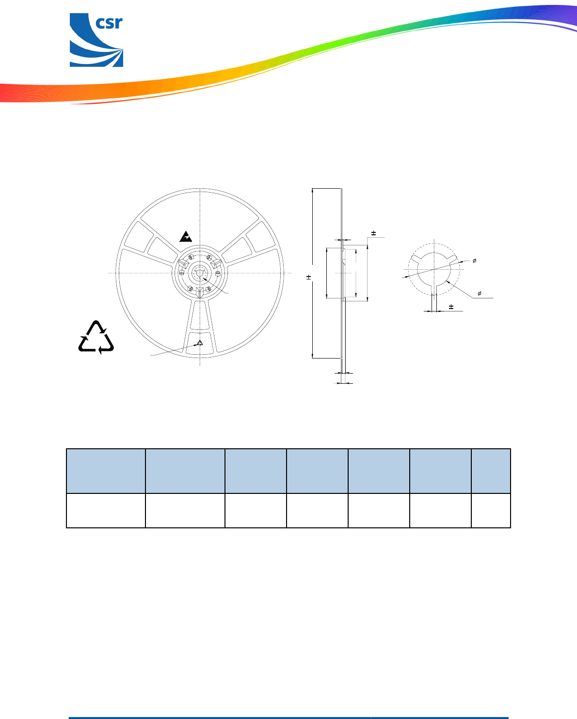
Figure 12.3: Reel Dimensions
Package Type
Nominal Hub
Width
(Tape Width)
a b W1 W2 Max Units
5 x 5 x 0.6mm
QFN 12 4.5 98.0 12.4
(2.0/-0.0) 18.4 mm
12.4 Moisture Sensitivity Level
CSR1010 QFN is qualified to moisture sensitivity level MSL3 in accordance with JEDEC J-STD-020.
Production Information
© Cambridge Silicon Radio Limited 2012
This material is subject to CSR's non-disclosure agreement
Page 38 of 42
CS-231985-DSP3
www.csr.com
CSR1010 QFN
Data Sheet
13 Document References
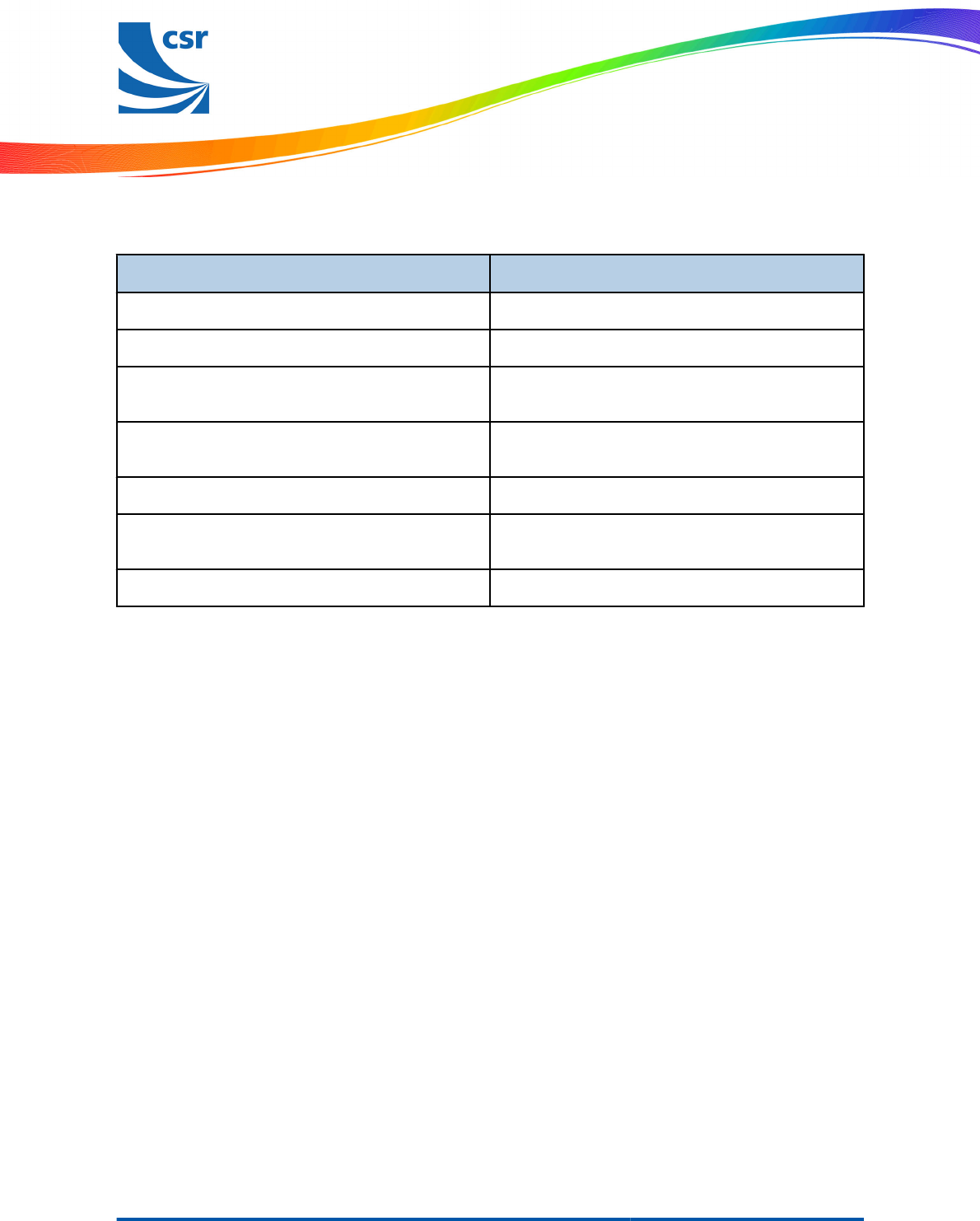
Document Reference, Date
Core Specification of the Bluetooth System.
Bluetooth Specification Version 4.0, 17 December 2009
CSR1010 QFN A05 Performance Specification.
CS-233372-SP
Electrostatic Discharge (ESD) Sensitivity Testing
Human Body Model (HBM).
JESD22-A114
Environmental Compliance Statement for CSR Green
Semiconductor Products.
CB-001036-ST
IC Packing and Labelling Specification.
CS-112584-SP
Moisture / Reflow Sensitivity Classification for
Nonhermitic Solid State Surface Mount Devices.
IPC / JEDEC J-STD-020
Typical Solder Reflow Profile for Lead-free Devices.
CS-116434-AN
Production Information
© Cambridge Silicon Radio Limited 2012
This material is subject to CSR's non-disclosure agreement
Page 39 of 42
CS-231985-DSP3
www.csr.com
CSR1010 QFN
Data Sheet
Terms and Definitions
Term Definition
AC Alternating Current
ADC Analogue to Digital Converter
AGC Automatic Gain Control
AIO Analogue Input/Output
ATT ATTribute protocol
balun balanced/unbalanced interface or device that changes a balanced output to an unbalanced
input or vice versa
Bluetooth
®
Set of technologies providing audio and data transfer over short-range radio connections
CSR Cambridge Silicon Radio
CTS Clear To Send
dBm Decibels relative to 1 mW
DC Direct Current
e.g.
exempli gratia
, for example
EDR Enhanced Data Rate
EEPROM Electrically Erasable Programmable Read Only Memory
EIA Electronic Industries Alliance
ESD Electrostatic Discharge
ESR Equivalent Series Resistance
GAP Generic Access Profile
GATT Generic ATTribute protocol
GSM Global System for Mobile communications
HID Human Interface Device
I²C Inter-Integrated Circuit Interface
I/O Input/Output
IC Integrated Circuit
IF Intermediate Frequency
IPC See www.ipc.org
IQ In-Phase and Quadrature
Production Information
© Cambridge Silicon Radio Limited 2012
This material is subject to CSR's non-disclosure agreement
Page 40 of 42
CS-231985-DSP3
www.csr.com
CSR1010 QFN
Data Sheet
Term Definition
JEDEC Joint Electron Device Engineering Council (now the JEDEC Solid State Technology
Association)
KB Kilobyte
L2CAP Logical Link Control and Adaptation Protocol
LC An inductor (L) and capacitor (C) network
LED Light-Emitting Diode
LNA Low Noise Amplifier
MAC Medium Access Control
MCU MicroController Unit
MISO Master In Slave Out
MLC MultiLayer Ceramic
MOSI Master Out Slave In
NSMD Non-Solder Mask Defined
PA Power Amplifier
PC Personal Computer
PCB Printed Circuit Board
PD Pull-down
PIO Parallel Input/Output
PIO Programmable Input/Output, also known as general purpose I/O
plc public limited company
ppm parts per million
PU Pull-Up
PWM Pulse Width Modulation
QFN Quad-Flat No-lead
RAM Random Access Memory
RF Radio Frequency
RISC Reduced Instruction Set Computer
RoHS Restriction of Hazardous Substances in Electrical and Electronic Equipment Directive
(2002/95/EC)
ROM Read Only Memory
RSSI Received Signal Strength Indication
Production Information
© Cambridge Silicon Radio Limited 2012
This material is subject to CSR's non-disclosure agreement
Page 41 of 42
CS-231985-DSP3
www.csr.com
CSR1010 QFN
Data Sheet
Term Definition
RTS Request To Send
RX Receive or Receiver
SIG (Bluetooth) Special Interest Group
SMP Security Manager Protocol
SPI Serial Peripheral Interface
TCXO Temperature Compensated crystal Oscillator
TX Transmit or Transmitter
UART Universal Asynchronous Receiver Transmitter
VCO Voltage Controlled Oscillator
W-CDMA Wideband Code Division Multiple Access
Production Information
© Cambridge Silicon Radio Limited 2012
This material is subject to CSR's non-disclosure agreement
Page 42 of 42
CS-231985-DSP3
www.csr.com
CSR1010 QFN
Data Sheet
FCC Statement
This equipment has been tested and found to comply with the limits for a Class B digital
device, pursuant to Part 15 of the FCC Rules. These limits are designed to provide
reasonable protection against harmful interference in a residential installation. This
equipment generates uses and can radiate radio frequency energy and, if not installed and
used in accordance with the instructions, may cause harmful interference to radio
communications. However, there is no guarantee that interference will not occur in a
particular installation. If this equipment does cause harmful interference to radio or television
reception, which can be determined by turning the equipment off and on, the user is
encouraged to try to correct the interference by one or more of the following measures:
-- Reorient or relocate the receiving antenna.
-- Increase the separation between the equipment and receiver.
-- Connect the equipment into an outlet on a circuit different from that to which the receiver is
connected.
-- Consult the dealer or an experienced radio/TV technician for help.
This device complies with part 15 of the FCC Rules. Operation is subject to the following two
conditions:
(1) This device may not cause harmful interference, and (2) this device must accept any
interference received, including interference that may cause undesired operation.
Changes or modifications not expressly approved by the party responsible for compliance
could void the user's authority to operate the equipment.