Microlise ML10 ML10 Tracking Unit User Manual Product Data Sheet
Microlise Limited ML10 Tracking Unit Product Data Sheet
Contents
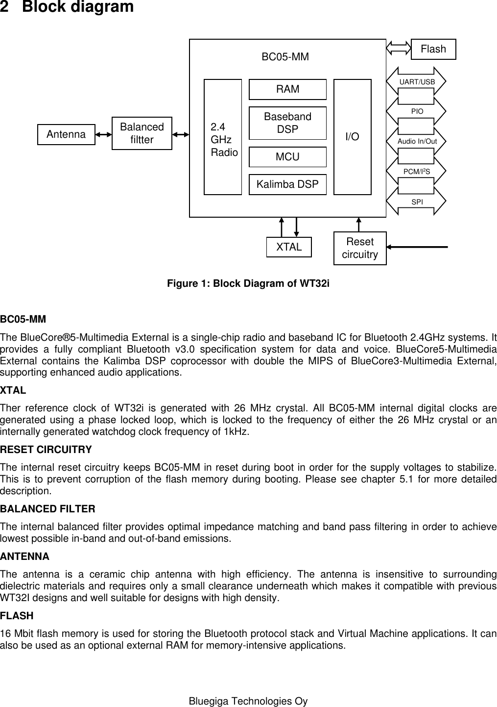
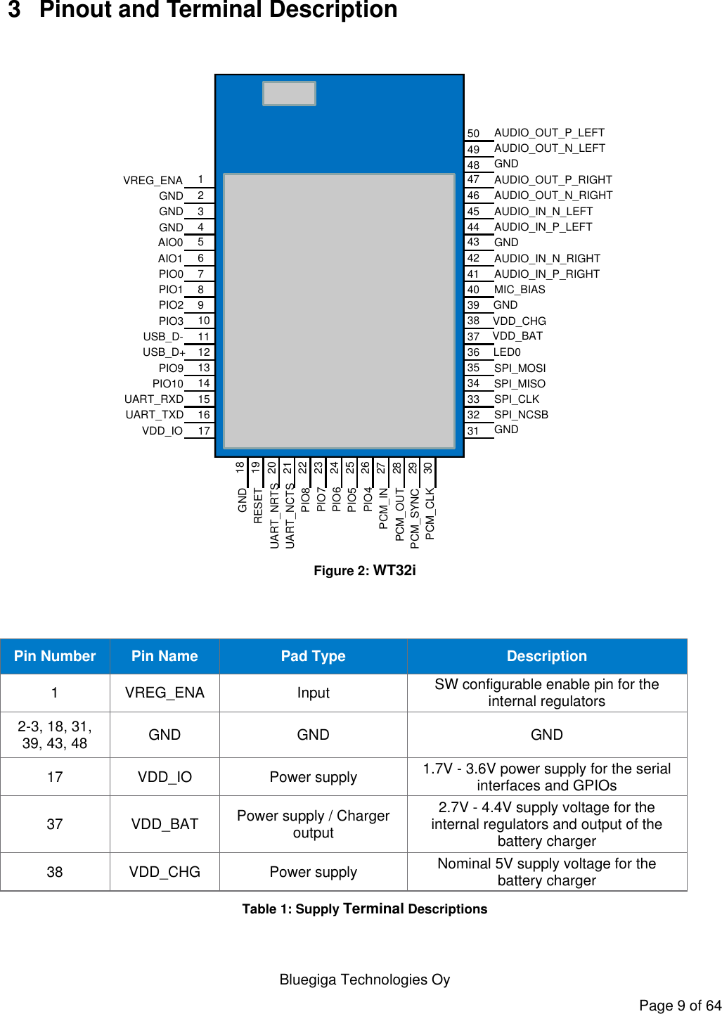
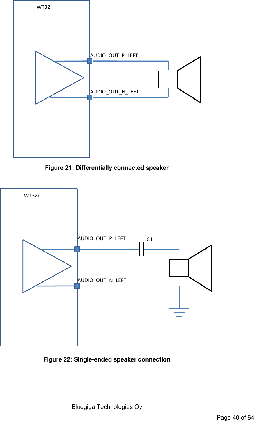
- 1. QOQWT32I Module - User Manual
- 2. User Manual
- 3. QOQBLE113 Module - User Manual
- 4. QIPEHS6 Module - User Manual
QOQWT32I Module - User Manual
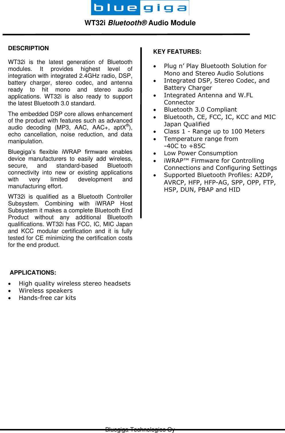

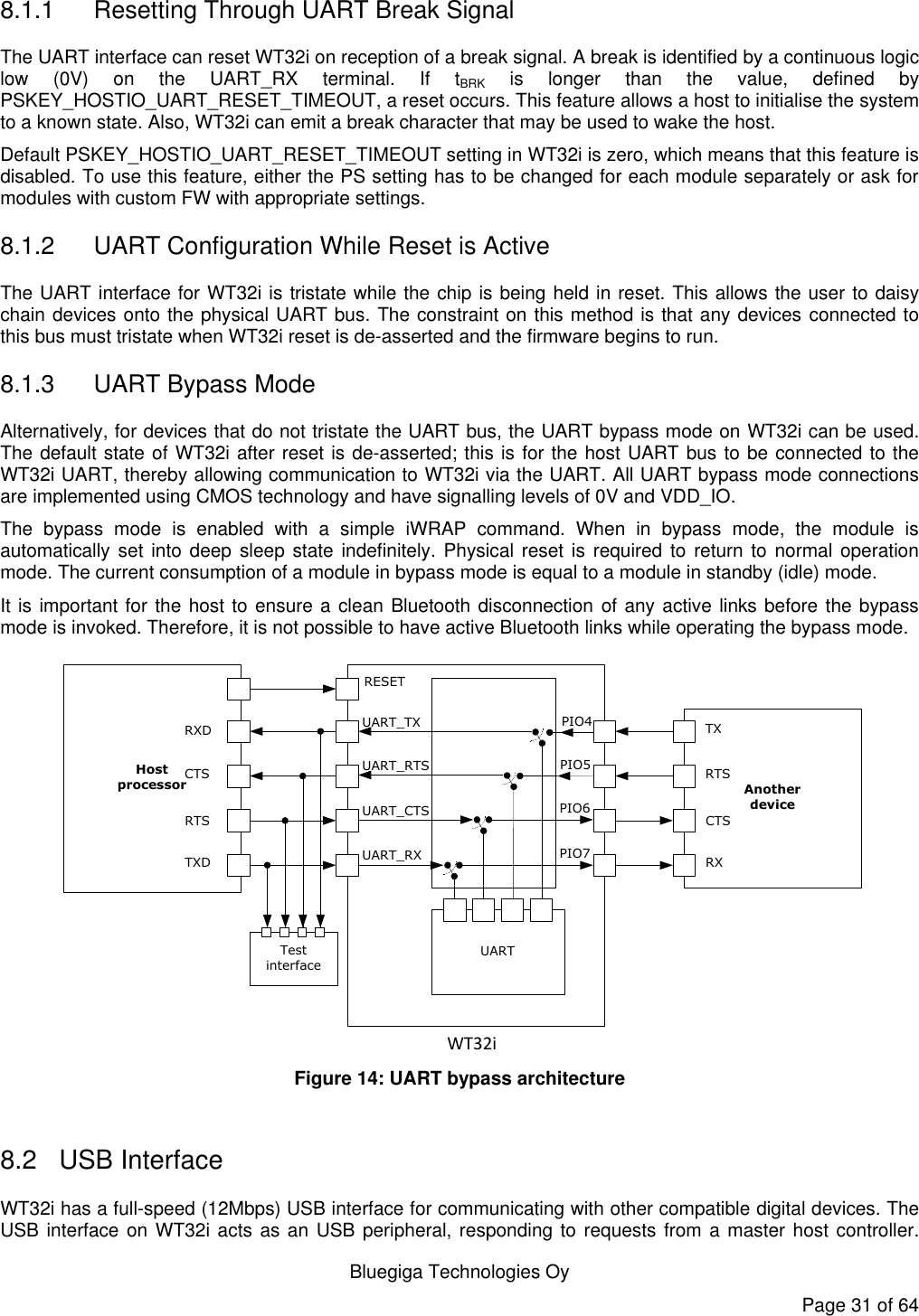
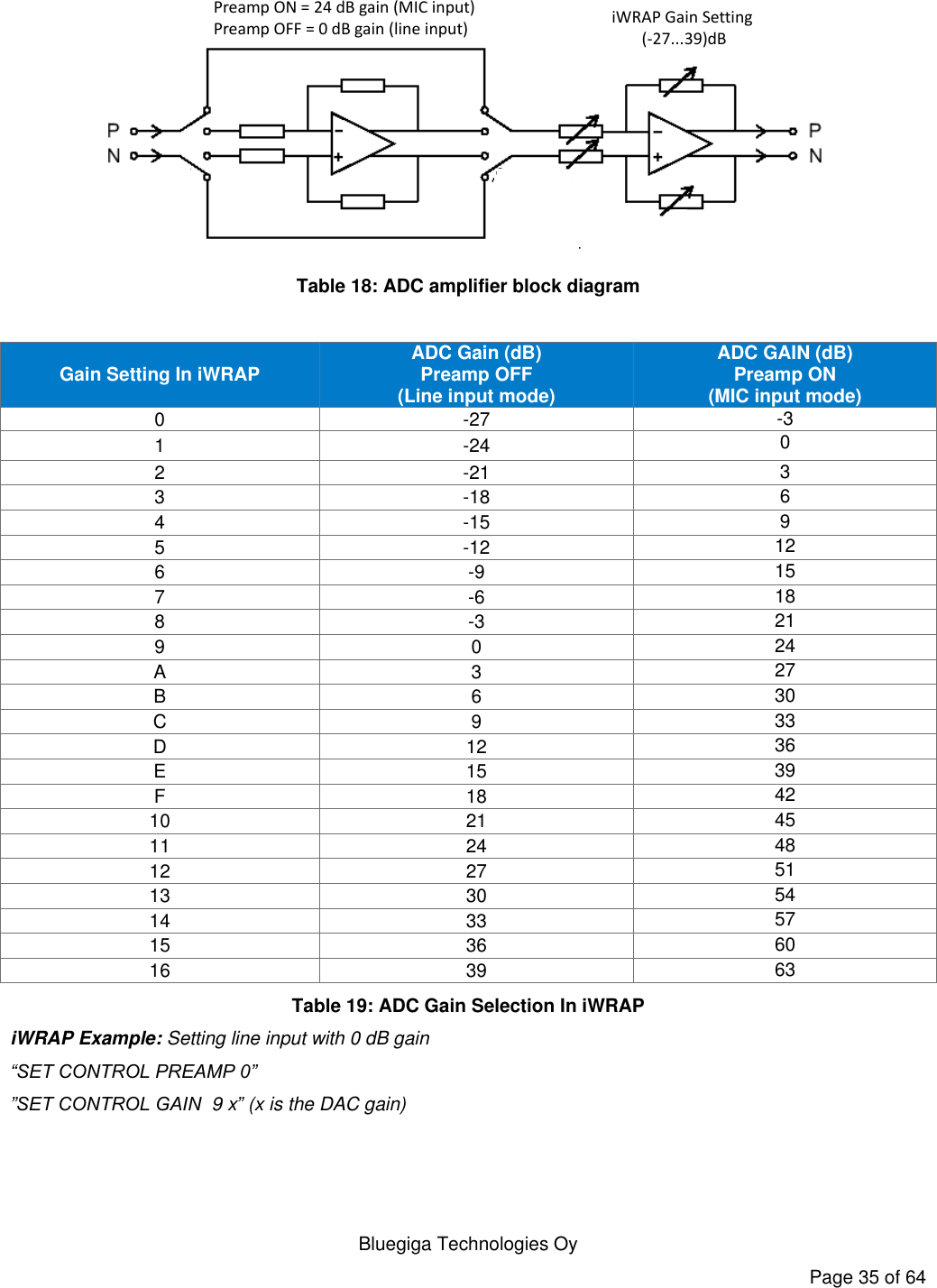
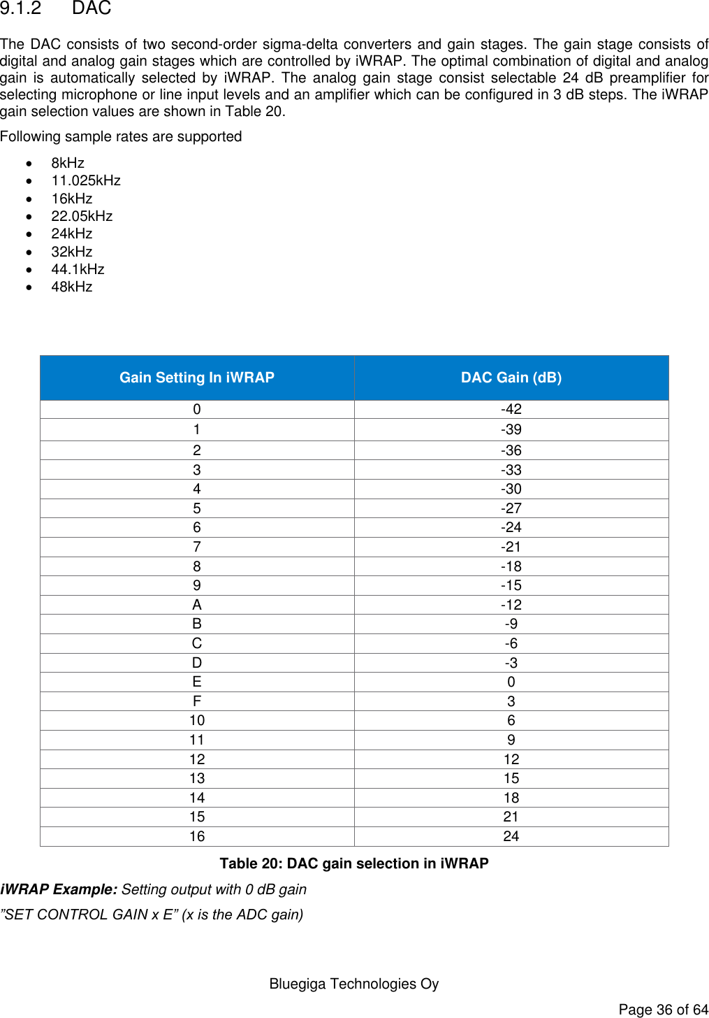
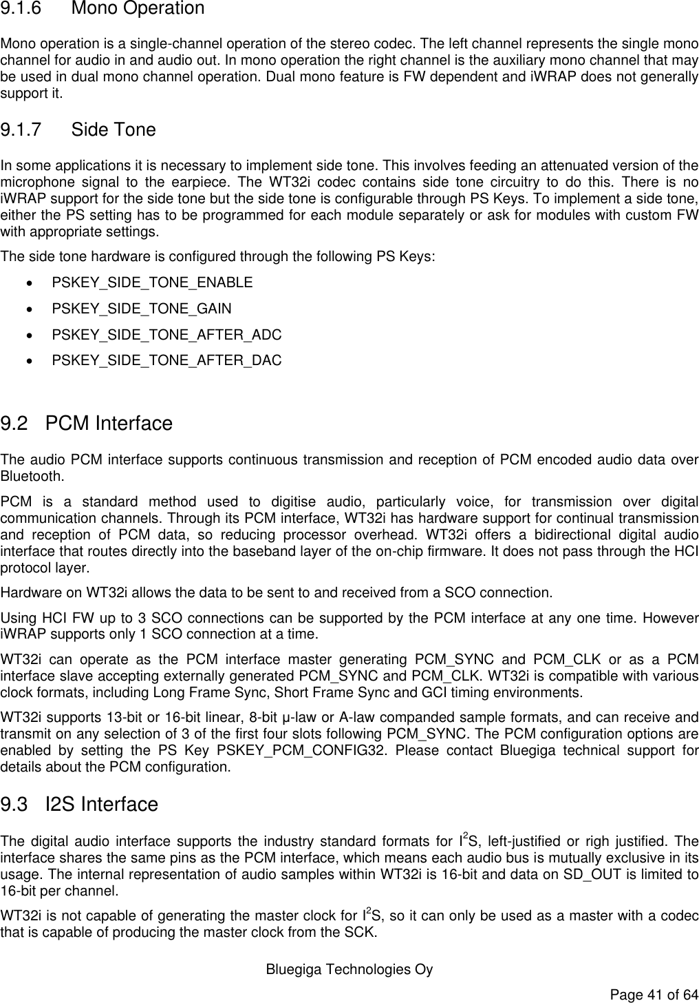
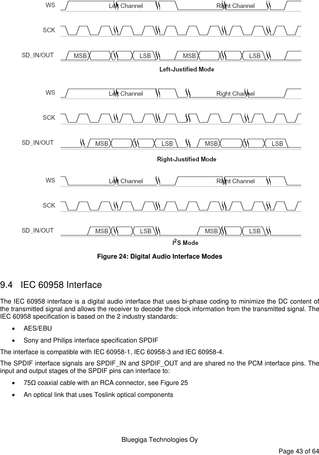
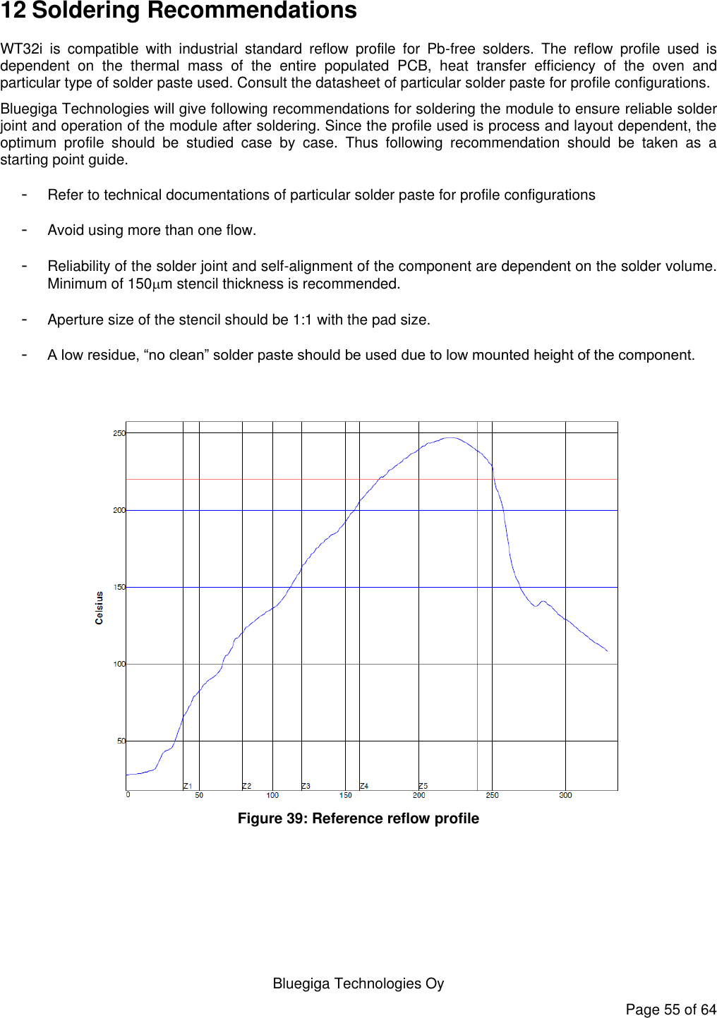
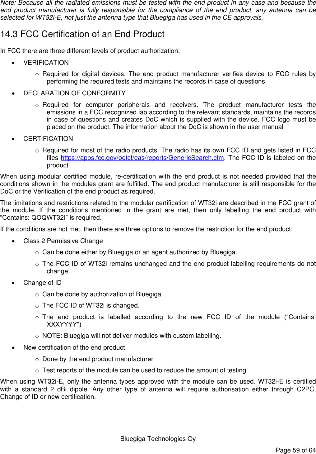
![Bluegiga Technologies Oy Page 42 of 64 WT32iWSSCKI2S_INI2S_OUTMCLK GeneratorASII2S CODEC Figure 23: I2S scheme for WT32i Bit Mask Name Description D[0] 0x0001 CONFIG_JUSTIFY_FORMAT 0 for left justified, 1 for right justified. D[1] 0x0002 CONFIG_LEFT_JUSTIFY_DELAY For left justified formats: 0 is MSB of SD data occurs in the first SCLK period following WS transition. 1 is MSB of SD data occurs in the second SCLK period. D[2] 0x0004 CONFIG_CHANNEL_POLARITY For 0, SD data is left channel when WS is high. For 1 SD data is right channel. D[3] 0x0008 CONFIG_AUDIO_ATTEN_EN For 0, 17-bit SD data is rounded down to 16bits. For 1, the audio attenuation defined in CONFIG_AUDIO_ATTEN is applied over 24bits with saturated rounding. Requires CONFIG_16_BIT_CROP_EN to be 0. D[7:4] 0x00F0 CONFIG_AUDIO_ATTEN Attenuation in 6dB steps. D[9:8] 0x0300 CONFIG_JUSTIFY_RESOLUTION Resolution of data on SD_IN, 00=16bit, 01=20bit, 10=24bit, 11=Reserved. This is required for right justified format and with left justified LSB first. D[10] 0x0400 CONFIG_16_BIT_CROP_EN For 0, 17-bit SD_IN data is rounded down to 16bits. For 1 only the most significant 16bits of data are received. Table 22: PSKEY_DIGITAL_AUDIO_CONFIG](https://usermanual.wiki/Microlise/ML10.QOQWT32I-Module-User-Manual/User-Guide-3202906-Page-42.png)