Midea Smart Technology 0003 Zigbee module User Manual UserManual
Midea Smart Technology Co., Ltd Zigbee module UserManual
UserManual

MM875033-11
zigbee Module
Datasheet
Revision Date Description Author
1.0 2016-11-11 initial release
contents
1. Introduction ........................................................................................................................... 3
1.1 1.1 Module System Block Diagram ...................................................................... 4
1.2 Module technical specifications ......................................................................... 5
2 Structure specification ........................................................................................................ 5
2.1 Module structure size .................................................................................................... 5
2.2 Hardware interface definition .................................................................................... 7
3 Wireless Specification ......................................................................................................... 8
1. Introduction
MM875033-11 is a low-power Zigbee module for the Internet of
Things,making the terminal more reliable, convenient and easy to
use.
The MM875033-11 module contains a NXP JN5169 single-chip
solution. the chip in software and hardware are used in low-power
technology, the purpose is to lower the power consumption of the
entire board, the product more competitive. The module makes up with
rf circuit, antenna, zigebee SOC, power supply, crystals and other
auxiliary circuit。At present, the module provides a complete serial
interface functions and equipment to communicate, so you can
through the serial port and mobile client to connect the cloud and
equipment.
2.4 GHz IEEE802.15.4 compliant
On-board antenna
2.0 V to 3.6 V battery operation
Power saving technology with low consumption
RX current 14.7 mA, in low power receive mode 13 mA
Configurable transmit power
Deep sleep current 140 nA (wake-up from IO)
Compensation for temperature drift of crystal oscillator frequency
The JN5169 features 512 kB embedded Flash, 32 kB RAM and 4 kB

EEPROM memoryand radio outputs up to 10 dBm.
1.1 1.1 Module System Block Diagram
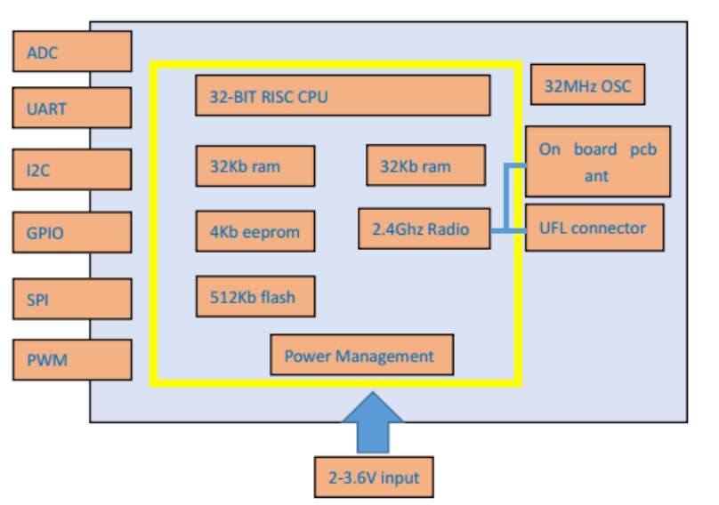
As shown in Figure 1, The MM875033-11 module contains a NXP
JN5169 single-chip solution, the chip highly integrated CPU, PMU, RAM,
Transceiver, LNA, PA, memmory, and other major parts, thus greatly
reducing the machine power, Amplitude reduces the layout area. The
module uses the internal antenna design in PCB, both for customers to
reduce the cost of the antenna, but also eliminates the need to
consider the antenna assembly space.
figure 1. Module System Block Diagram

1.2 Module technical specifications
Main chip
JN5169
Working frequency
2.40~2.485GHz
Supported standard
IEEE802.15.4
Modulation
O-QPSK MODEM
communication interface
UART
PCB layer structure
4 Layer
PCB size
22mm(L)x17mm(W)x2.0mm(H)
Antenna
PCB internal antennas
Operation temperature
0℃~+85℃
Storage temperature
-40℃~+125℃
Hardware version number
Msmart-Zigbee(JN5169)-A[V1.1]
2 Structure specification
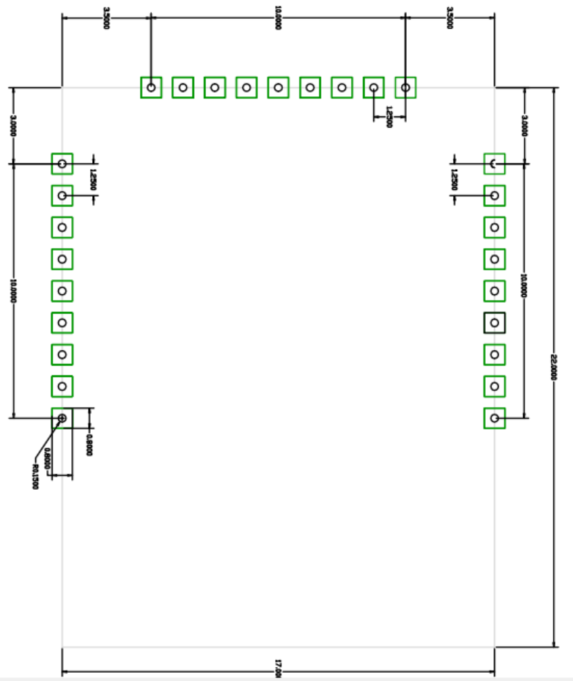
2.1 Module structure size

The size of the module as shown above, length 22mm, width 17mm, thickness
2.0mm (error +/- 0.2mm)

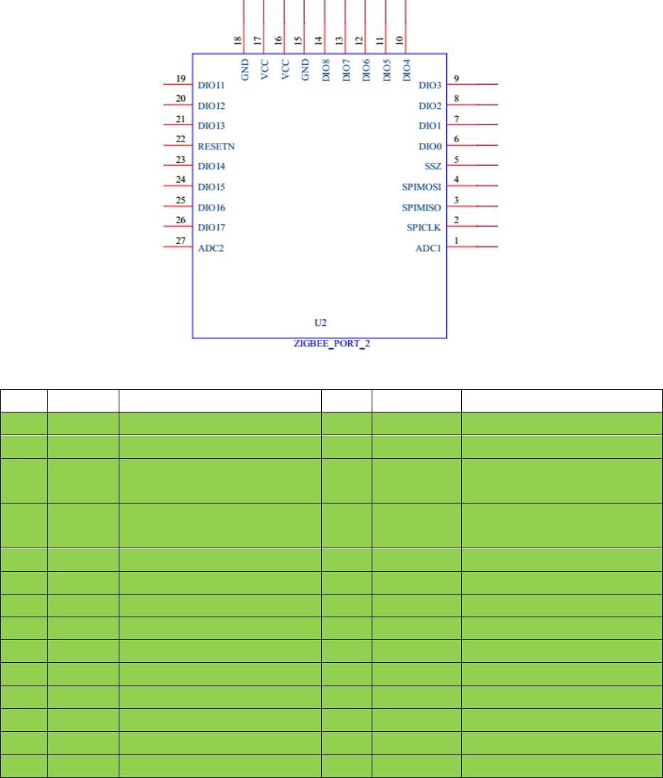
2.2 Hardware interface definition
1
ADC1
ADC INPUT 1
15
GND
Ground
2
SPICLK
SPI BUS master clock out
16
VCC
Supply Input Pin
3
SPIMISO
SPI BUS master in,slave out
input
17
VCC
Supply Input Pin
4
SPIMOSI
SPI BUS master out,slave in
output
18
GND
Ground
5
SSZ
SPI BUS master select output 0
19
DIO11
GPIO
6
DIO0
GPIO&ADC INPUT 3
20
DIO12
GPIO
7
DIO1
GPIO& ADC INPUT 4
21
DIO13
GPIO
8
DIO2
GPIO& ADC INPUT 5
22
RESETN
Reset pin,Active Low
9
DIO3
GPIO& ADC INPUT 6
23
DIO14
UART1-TX&I2C-SCL
10
DIO4
GPIO
24
DIO15
UART1-RX&I2C-SDA
11
DIO5
GPIO
25
DIO16
I2C-SCL &GPIO
12
DIO6
UART0-TX
26
DIO17
I2C-SDA &GPIO
13
DIO7
UART0-RX
27
ADC2
ADC INPUT 2
14
DIO8
GPIO

3 Wireless Specification
reference section limit
Transmission
TX Maximum Power ETSI EN 300 328 4.3.2.1 20dBm
TX Spurious 30Mhz-1Ghz ETSI EN 300 328 4.3.2.8 -36 or -54dbm(depends on
frequency)(100khz BW)
ETSI EN 300 328 4.3.2.8 -30 dBm
ECM 802.15.4 10.3.8 35%
TX Frequency Tolerance 802.15.4 10.3.9 +/-40 ppm
min of max power 802.15.4 10.3.10 -3dBm
phase noise(unspread) No reference
Reception
RX spurious 30Mhz - 1GHz ETSI EN 300 328 4.3.2.9.2 -57dBm(100 Khz)
RX spurious 1G - 12.5GHz ETSI EN 300 328 4.3.2.9.2 -47 dBm(1 Mhz)
RX sensitivity 802.15.4 10.3.4 -85dBm
Interference rejection
N+/-1(adjacent) 802.15.4 10.3.5 0dB
Interference rejection
N+/-2(alternate) 802.15.4 10.3.5 30dB
RX Max input 802.15.4_2011 10.3.11 -20dBm
FCC Statement
This equipment has been tested and found to comply with the limits for a Class B digital device, p
ursuant to part 15 of FCC Rules. These limits are designed to provide reasonable protection again
st harmful interference in a residential installation. This equipment generates and can radiate radi
o frequency energy and, if not installed and used in accordance with the instructions, may cause
harmful interference to radio communications. However, there is no guarantee that interference
will not occur in a particular installation. If this equipment does cause harmful interference to rad
io or television reception, which can be determined by turning the equipment off and on, the use
r is encouraged to try to correct the interference by one or more of the following measures:
Reorient or relocate the receiving antenna.
Increase the separation between the equipment and receiver.
Connect the equipment into an outlet on a circuit different from that to which the receiver is con
nected.
Consult the dealer or an experienced radio/TV technician for help.
This device complies with Part 15 of FCC Rules. Operation is subject to the following two conditio
ns: (1) This device may not cause harmful interference, and (2) This device must accept any interf
erence received, including interference that may cause undesired operation.

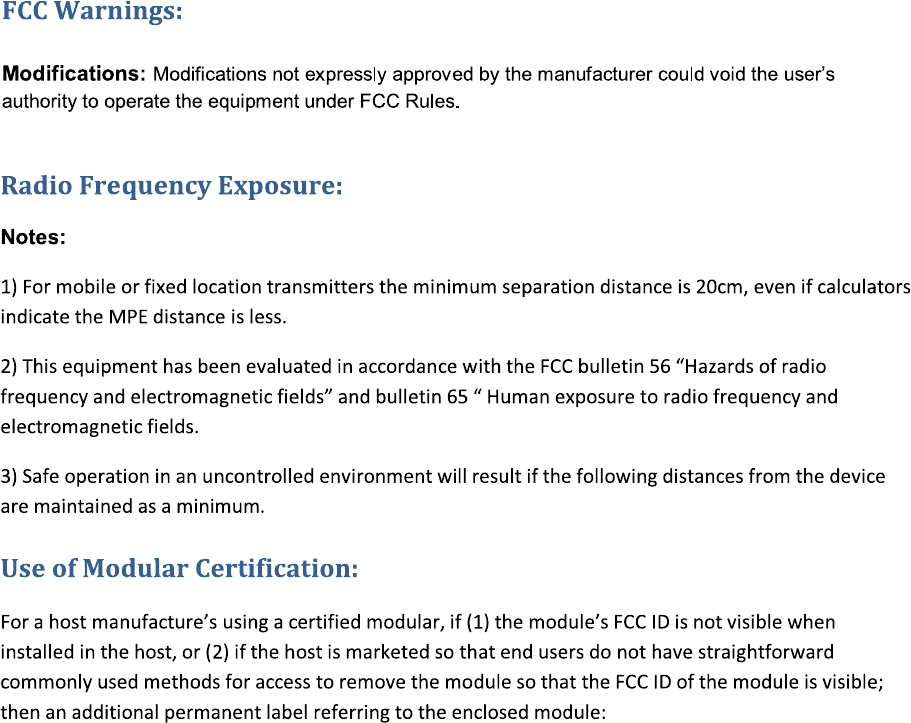
"Contains Transmitter Module FCC ID:2AIRV0003" or "Contains FCC ID:2AIRV0003" must be used.