Midland Radio SD125V3 Data Radio User Manual Design Docs
Midland Radio Corporation Data Radio Design Docs
users manual

Topaz3, LLC. 10828 N.W. Airworld Dr. Kansas City, MO 64153 Tel: 816-891-6320 Fax: 816-891-8815
August 2002
User
Guide
SD 125V3 DATA RADIO

SD 125V3
Page -1-
August 2002
THEORY OF OPERATION
THEORY OF OPERATION
The SD 125V3 radio is comprised of two PCB's (an RF PCB and a digital PCB).
These boards are connected with an 18 pin female and male connector. The digital
board is interfaced with external data equipment through the 9 pin d-sub male connec-
tor, which controls the radio and data receiving and sending.
DIGITAL CIRCUIT
The digital circuit is charged to be control for all of the signal path and set the frequen-
cies to be set and selecting the desired channel.
TX-Signal circuit The TX data signal comes from Pin 2 of Con 401, and goes through U404D. The TX-
signal is amplified by U406C. The TX-signal is filtered by U405A & B which is a 4'th
order low pass filter, therefore, the filtered signal supply to the RF board for TX modu-
lation.
RX-Signal Circuit The RX- data signal comes from the RF board, which is connected with pin 10 of Con
403. The RX-signal is switched by U404A and adjusted by RV403 and amplified by
U407. The amplified signal goes to pin10 of Con 401.
RSSI Detector From the RF board, the RSSI (Received Signal Strength Indicator ) signal comes to
U403A & B through R461. The pulse is injected from pin 5 of U403B every 1 ms and
C451 is discharged. After then, it begins to be charged by R464. Simultaneously,
RSSI signal is input to pin 7 of U403A and those signals are compared. The compared
signal is output from U403A. Pin 1 and the CPU detects the pulse width. The pulse
width is varied by RSSI DC voltage. Therefore, the CPU determines the carrier detec-
tion .
EEPROM RX. TX channel and RSSI detection level as well as other data from the programmer
are stored in the EEPROM. The data stored is retained without power supplied. This
is a non-volatile memory . The EEPROM may have information re-programmed or
erased. U402 is an EEPROM with 2048 capacity and data is written and read serially.
Channel Selector One of 16 channels may be selected using the clip switch named SW401 . SW401
encodes the channel number, selected into 4-bit binary code. The binary code plus
one equals the channel number. The binary code is decoded by the CPU enabling the
appropriate RX or TX frequency and associated data to be selected from the
EEPROM. In the binary bit of SW401, the lower 2 bits are connected to Con402. It
causes the low 4 channels to be selected from the external equipment's.
DC to DC Converter The main DC power is injected to the DC to DC converter . The DC to DC converter
regulates the various input power supply voltage and outputs a constant voltage of 7.5
Volts. It is a source for all of the RF and digital circuits.
The DC to DC converter is formed by U801, Q801, Q802, L801 and R804. U801 is a
switch mode DC to DC Converter IC. Input DC various appears as a voltage various
through R804. U801 detects the voltage and controls the switching pulse. As the
switching pulses, Q801and Q802 switches the input DC of various supply voltages
and generates the constant DC of supply voltage.

SD 125V3
Page -2-
August 2002
THEORY OF OPERATION
RF CIRCUITS
TRANSMITTER
The transmitter is comprised of:
1. Buffer
2. P.A Module
3. Low Pass Filter
4. Antenna Switch
5. A.P.C Circuits
Buffer VCO output level is -6dBm and amplified to, +6dBm. The buffer consists of Q16 and
Q17 for isolation and gain.
P. A . M o d u l e The P.A Module contains Q501, Q502, and Q503. Three stage amplifier Q501 ampli-
fies the TX signal from +10 dBm to 100 mW. Q502 is amplified to 0.5W. Q503 ampli-
fies to 3W and then matched to 50 OHMs using the L.C. network, thereby reducing
the harmonics by -30 dB.
Low Pass Filter L7, L8, L11, C72, C73, C74 and C75 are the 7th order Chebyshev low pass filter.
Unwanted harmonics are reduced by -70 dBc.
Antenna Switch When transmitting, the diodes D5 and D6 are forward biased enabling the RF signal
passage to the antenna. D6 is shorted to ground inhibiting the RF signal to front end.
In receive the diodes D5 and D6 are reversed biased passing the signal from the
antenna through L13 and C83 to the front end without signal loss.
Automatic Current
Control (ACC) Circuits
The ACC circuit consists of R109, variable resistor RV1, IC3(B) and transistors Q21
and Q22. The supply current is monitored by the difference voltage on R109 (0.1
Ohm). If the current varies by RF power output or other reasons, it produces some
bias voltage by IC3A and Q19. The differential signal at the output of IC3 is passed to
Q21 and Q22 that produces a constant power output to the antenna. RV1 is used to
adjust the RF power level.
RF CIRCUITS PLL SYNTHESIZER
12.8 MHz TCXO The TCXO contains the 3-stage thermistor network compensation and crystal oscilla-
tor and modulation ports. Compensation is +/-5 PPM or less from -30c to +60c.
PLL IC Dual Modules
Prescaler
Input frequency of 12.8 MHz to IC2 MC14519 pin 20 is divided to 6.25 KHz or 5 KHz
by the reference counter, and then supplied to the comparator. RF signal input from
VCO is divided to 1/64 at the prescaler in IC2, divided by A and N counter in IC2 to
determine frequency steps, and then supplied to the comparator. PLL comparison
frequency is 6.25/5KHz so that minimum programmable frequency step is 5/6.25 KHz.
The A and N counter is programmed to obtain the desired frequency by serial data in
the CPU. In the comparator, the phase difference between reference and VCO signal
is compared. When the phase of the reference frequency is leading , Fv is the output,
but when VCO frequency is leading, Fr is the output. When Fv=Fr, phase detector out
is a very small pulse. 64/65 modulus prescaler is comprised in IC2, and has two out-
put ports:
Port A pin 16: TX enable 2

SD 125V3
Page -3-
August 2002
THEORY OF OPERATION
Port B pin 15: prescaler power save control in PLL IC Pin 13 labeled test2 allows the
technician to see the output of the dual modulus prescaler for trouble shooting pur-
poses, no connection should be made to this pin.
Level Shifter & Charge
Pump
The charge pump is used for changing output signals Fr, Fv at PLL IC from 0-5v to 0-
12v necessary for controlling the VCO.
Reference Frequency
LPF
The Loop Filter contains R12, C21 and C22. LPF settling time is 12mS with 1 KHz fre-
quency. This also reduces the residual side-band noise for the best signal-to-noise
ratio.
DC to DC Converter The DC to DC converter convert the 5v to 14-16v to supply the necessary voltage for
wide range frequency in the VCO.
VCO The VCO consist of an RX VCO and a TX VCO. It is switched TX/RX by the power
source. It is configured as a colpits oscillator and connected to the buffer as a cascade
bias in order to save power. The varicap diode D201/D301 are low-resistance ele-
ments and produce a change in frequency with a change in reverse bias voltage (2-
11v). L203/L303 are resonant coils, which changes the control voltage by the tuning
core. D202 modulation diode, modulates the audio signal. C204 compensates for the
non-linearity of the VCO due to modulation diode, and maintains a constant modula-
tion regardless of frequency .
RECEIVER
Front End The receive signal is routed backward through the low pass filter, then onward to Pin 1
of the Hybrid Receiver Front End Module to a bandpass filter consisting of C622
through C608, L607 through L604 is coupled to the base of Q601 which serves as an
RF amplifier. Diode D601 serves as protection from static RF overload from nearby
transmitters. The output of Q601 is then coupled to a second bandpass filter consist-
ing of C607 through C623 and L604 through L607.The output of Pin 6 is then coupled
to the doubly balanced mixer D9. The receiver front end module is factory pre-tuned
and requires no adjustment. Repair is effected by replacement of the entire module of
the proper banded module. The receiver front end module signal pins are as follows:
1. RF Input
2. Input Ground
3. N/A
4. Receive +5V
5. Ground
6. Output
First Mixer D9, T2 and T3 are double balanced mixers which provide the 45.1 MHz intermediate
frequency output. The filtered frequency from the front end module is coupled to T2 .
The 45.1 MHz IF output is matched to the input of the 2-pole monolithic filter by L14,
L31, C69 and C97. The crystal filter provides a bandwidth of +/-7.2 KHz from the oper-
ating frequency providing a high degree of spurious and intermodulation protection.
Additionally, a 90 MHz trap (XF1) is also placed at the filter output to provide addi-
tional attenuation of the second order IMD. The output of the filter is impedance
matched by C97 and C69 to the base of the post of filter IF amplifier Q25.
Second Oscillator
Mixer Limiter And FM
Detector
The output of the post filter amplifier, Q25, is coupled via C98 to the input of IC5 (
MC3371). IC5 is a monolithic single conversion FM transceiver, containing a mixer,
the second local oscillator, limiter and quadrature detector. Crystal X1 44.645 MHz is

SD 125V3
Page -4-
August 2002
THEORY OF OPERATION
used to provide resultant 455KHz signal from the output of the second mixer. The
mixer output is then routed to CF1 ( 455F). These ceramic filters provide the adjacent
channel selectivity of 25 KHz bandwidth .
RSSI ( Receiver Sig-
nal Strength Indicator
)
The RSSI signal is output from IC5 on pin 13. As the receiver signals the output, DC
voltage is varied as much as receiver signal strength. Also, the DC signal is tempera-
ture compensated with a thermistor (THI ).
SD 125V3
Page -5-
August 2002
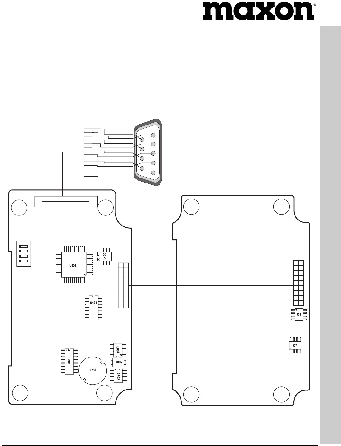
WIRING DIAGRAM
WIRING DIAGRAM
SW401
CON1CON403
1234
1
1718
2
1
1718
2
D-SUB 9 CONNECTOR
(P/N 950-010-0033)
Pin1. ....Audio In (Data RX)
Pin2. . . . . Audio Out (Data TX)
Pin3.....PTT
Pin4. . . . . GND (Ground)
Pin5. ....B+ (8-18 Volts DC)
Pin6. . . . . Carrier Detect
(Squelch)
Pin7. ....N/C No Connect
1
2
3
4
5
6
7
8
9
10
11
12
13
14
15
6
1
7
2
8
3
9
4
5
115
CON401
DIGITAL BOARD
RF BOARD
Page -6-
August 2002
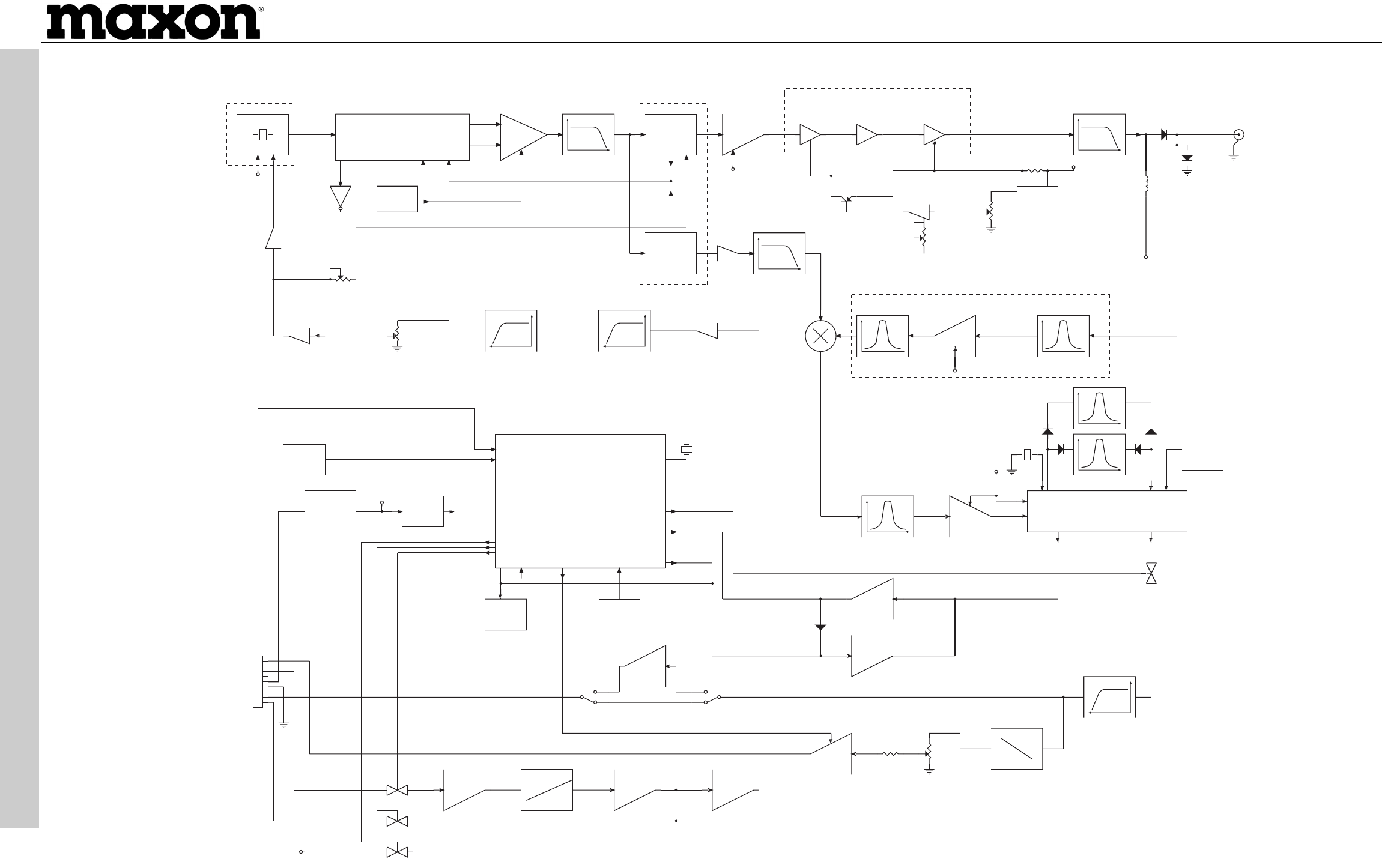
BLOCK DIAGRAM
BLOCK DIAGRAM
ANT
L.P.F
D5
ANT SW
Q502
Q501 Q503
P.A. MODULE
Q16/Q17
TX BUFFER
Q202/203
TX VCO
CONT
C21,C22
REF L.P.F TX VCO
#R
LEVEL SHFTER
Q6,7,8,11
Ref Freg
IC2
PLL CIRCUIT
PLL EN
TCXO1
TCXO(12.8MHz)
TCXO
TCXO MOD
+5V
L/D
Q5
RV401
BALANCE
INVERTER
#V
DATA
CPU
DC/DC CONVERTER
F in
16V
TX 5V
Q12
RX BUFEFER L1,L2
LOCAL LPF
CONT RX VCO
Q302/303
MOD
IC3B
AUTO POWER CONTROL
Q22
CONTROL
RV1
POWER ADJUST
HI
FROM CPU
RV6
POWER ADJUST
LOW
D6
VCC
IC3A
CURRENT DETECTOR
CONVERT
CURRENT SENSOR
TX B+
FILTER
CF1
2nd IF FILTER
25KHz
FILTER
RX
5V
FRONT-END
T2/3/D9
MIXER
Q601
LOW NOISE AMP
RX VCO
BUFFER
U405B
2nd LPF
U405A
2nd LPF
RV2
MOD LEVEL
IC405B
BUFFER
CH SEL
D/D CONVERTER
Vin 7.5V-25V
Vout 7.5V
CHANNEL
L/D
IC1
5V REGULATOR
5V
VCC 68HC705C8
X401
3.57
TCAP
DATA EN
U401
RX +5V
1st IF FILTER
45.1MHz
Q25
1st IF AMP
XF1
MIXER
INPUT
455KHz
T1
QUADRATURE
X1
2nd LOCAL
44.645MHz
CF2
2nd IF FILTER
12.5KHz
RSSI OUT DATA OUT
3KHz LPF
U406B
1
2
13
U404A
U403A
LM339
U403B
LM339
RSSI SQUELCH CONTROL
PA0
U408
RESET
LK2/LK3LK9/LK10
U409
COMPARATOR
IC408
EEPROM
386 EN
1
2
3
4
5
6
7
8
9
DB9
DB9 CABLE
U405D
PREMPHSIS
89
6
U404D
1110
1
2
U404B
U405C U406C CPU AF MUTE
R454/C422
DEMPHASIS
RV403
AF LEVEL
U407
LM386
AUDIO AMP
43
5
U404C
TX TONE
Page -7-
August 2002
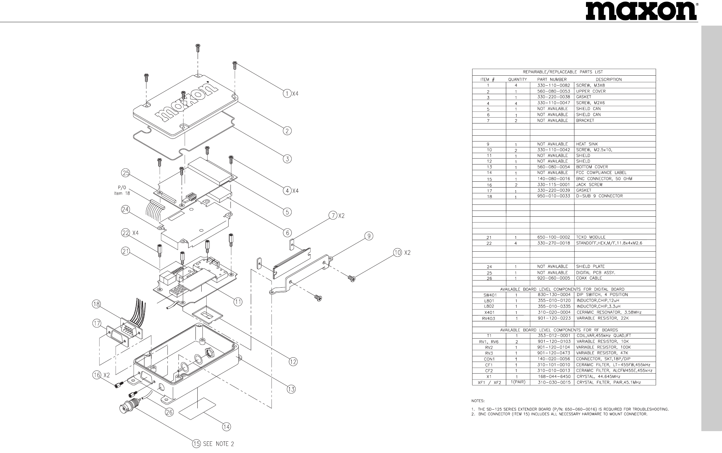
EXPLODED VIEW
EXPLODED VIEW