Mindray BIO Medical electronics WM1010BGN10 Cyberlink User Manual Cyberlink Wireless LAN Module datasheet
Shenzhen Mindray BIO-Medical electronics Co.,LTD. Cyberlink Cyberlink Wireless LAN Module datasheet
Users manual
KF-XXXX-X-XXX-版本
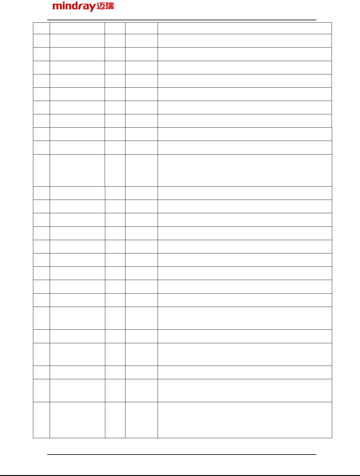
No.
Pin name Type
System Description
1 SD_CLK I WLAN SDIO Clock.
2 VIN I Common
3.3V Power supply input.
3 SD_CMD I/O WLAN SDIO Command Line.
4 GND I Common
Ground.
5 SD_D0 I/O WLAN SDIO Data Line 0.
6 /WL_RESET I WLAN Low asserting reset for WLAN core.
7 SD_D1 I/O WLAN SDIO Data Line 1.
8 SLEEP_CLK I Common
Low Power Clock input (32.768kHz).
9 SD_D2 I/O WLAN SDIO Data Line 2.
10
POW_ON I Common
Used by PMU to decide whether or not to power down
internal BCM4329 regulators. If POW_ON is low, then the
regulators will be disabled.
11
/CD O Common
Cyberlink On-line Detect. PIN tie to ground.
12
NC No use
13
SD_D3 I/O WLAN SDIO Data Line 3.
14
VIN I Common
3.3V Power Input
15
LED O Common
3.3V Output
16
VIN I Common
3.3V Power Input
17
GND I Common
Ground.
18
GND I Common
Ground.
19
WL_WAKE_IN I WLAN WLAN device wake-up signal input from host to WLAN.
20
BT_UART_TXD
O BT Bluetooth UART serial output .Serial data output for the HCI
UART interface.
21
NC No use
22
BT_UART_RXD
I BT Bluetooth UART serial input. Serial data input for the HCI
UART interface.
23
NC No use
24
BT_UART_RTS
O BT Bluetooth UART request to send. Active-low request-to
send signal for the HCI UART interface.
25
SW1 I Common
Antenna select.
SW1 and SW2 are floating, Select antenna 1
SW1=1,SW2=0,Select antenna 1
KF-XXXX-X-XXX-版本
SW1=0,SW2=1,Select antenna 2
26
BT_UART_CTS
I BT Bluetooth UART clear to send. Active-low clear-to-send
signal for the HCI UART interface.
27
SW2 I Common
Antenna select.
SW1 and SW2 are floating, Select antenna 1
SW1=1,SW2=0,Select antenna 1
SW1=0,SW2=1,Select antenna 2
28
TYPE O Common
Cyberlink type Detect. PIN tie to 3.3V.
29
GND I Common
Ground.
30
VIN I Common
3.3V Power Input
31
/BT_RESET I BT Low asserting reset for Bluetooth core.
32
BT_WAKE_IN I BT
Bluetooth device wake-up signal input from host to
Bluetooth. The polarity of this signal is software
configurable and can be asserted high or low.
33
BT_WAKE_OUT
O BT Host wake-up signal output from WLAN to host.
34
GND I Common
Ground.
35
NC Tie 10k to ground
36
WL_WAKE_OUT
O WLAN Host wake-up signal output from WLAN to host.
37
BT_PCM_CLK I/O BT PCM clock, can be master (output) or slave (input).
38
NC Reserved for MIMO
39
BT_PCM_SYNC
I/O BT PCM sync signal, can be master (output) or slave (input).
40
GND I Common
Ground.
41
BT_PCM_OUT I BT PCM data input.
42
NC No use
43
BT_PCM_IN O BT PCM data output.
44
NC Reserved for MIMO
45
NC No use
46
NC Reserved for MIMO
47
NC No use
48
NC No use
49
WL_TXD O WLAN TX pin of debug UART
50
NC No use
KF-XXXX-X-XXX-版本
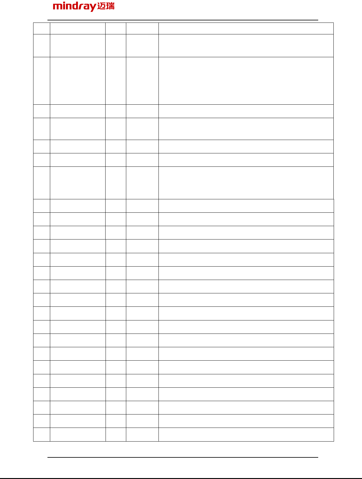
51
WL_RXD I WLAN RX pin of debug UART
52
NC No use
1.7.2 Power On Sequence
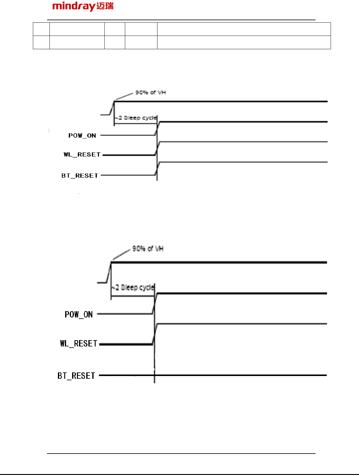
1.7.2.1 Power On Sequence 1
Figure 2 Power On Sequence 1
1.7.2.2 Power On Sequence 2
Figure 3 Power On Sequence 2
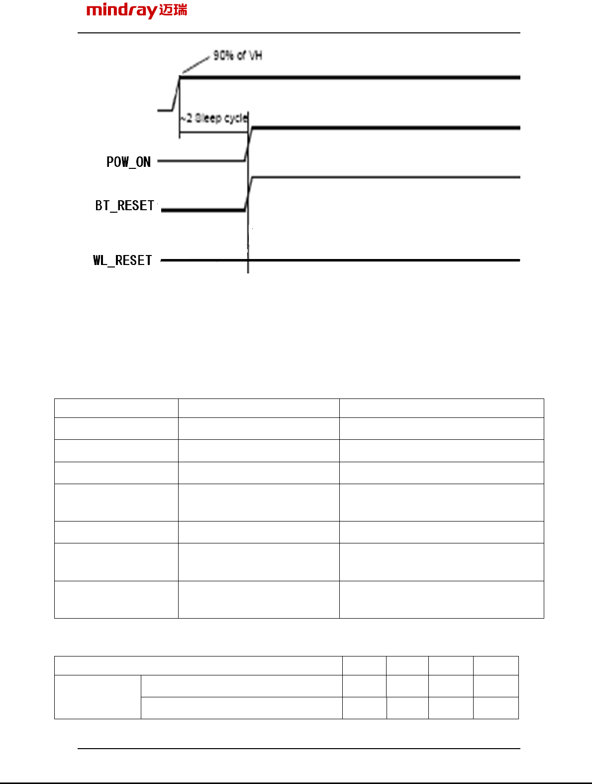
1.7.2.3
Power On Sequence
3
VIN
VINVIN
VIN
VIN
VINVIN
VIN
KF-XXXX-X-XXX-版本
Figure 4 Power On Sequence 3
1.7.3 Interface
1.7.3.1 External Clock Reference (
SLEEP_CLK
)
Table 7 External Clock Reference
Parameter Description Remarks
Nominal input frequency
32.768 KHz
Frequency accuracy +/-200 ppm
Duty cycle 30-70 %
Input signal amplitude 200 to 1800 mVp-p 200-1800 mVp-p to avoid additional
current consumption. 3.3Vp-p maximum.
Signal type Square-wave or sine-wave
Input impedance 100KΩ;< 5 pF when power is
applied or power is off
Clock jitter (integrated
over 300Hz – 15kHz)
<1 Hz
1.7.3.2 Input/Output DC Terminal Characteristics
Table 8 Input/Output DC Terminal Characteristics
Digital Terminals Min Typ Max Unit
V
IL
input logic level low - - 0.8 V
Input Voltage V
IH
input logic level high 2.0 - - V
VIN
VINVIN
VIN
VIN
VINVIN
VIN
KF-XXXX-X-XXX-版本
V
OL
output logic level low (100μA load) - - 0.4 V
Output Voltage V
OH
output logic level high (-100μA load)
2.4 - - V
I
IL
input logic level low - 0.3 - uA
Input Current: I
IH
input logic level high - 0.3 - uA
I
OL
output logic level low (V
OL
=0.4V) - - 3.0 mA
Output Current I
OH
output logic level high (V
OH
=2.9V) - - 3.0 mA
Input Capacitance :C
IN
- - 5 pF
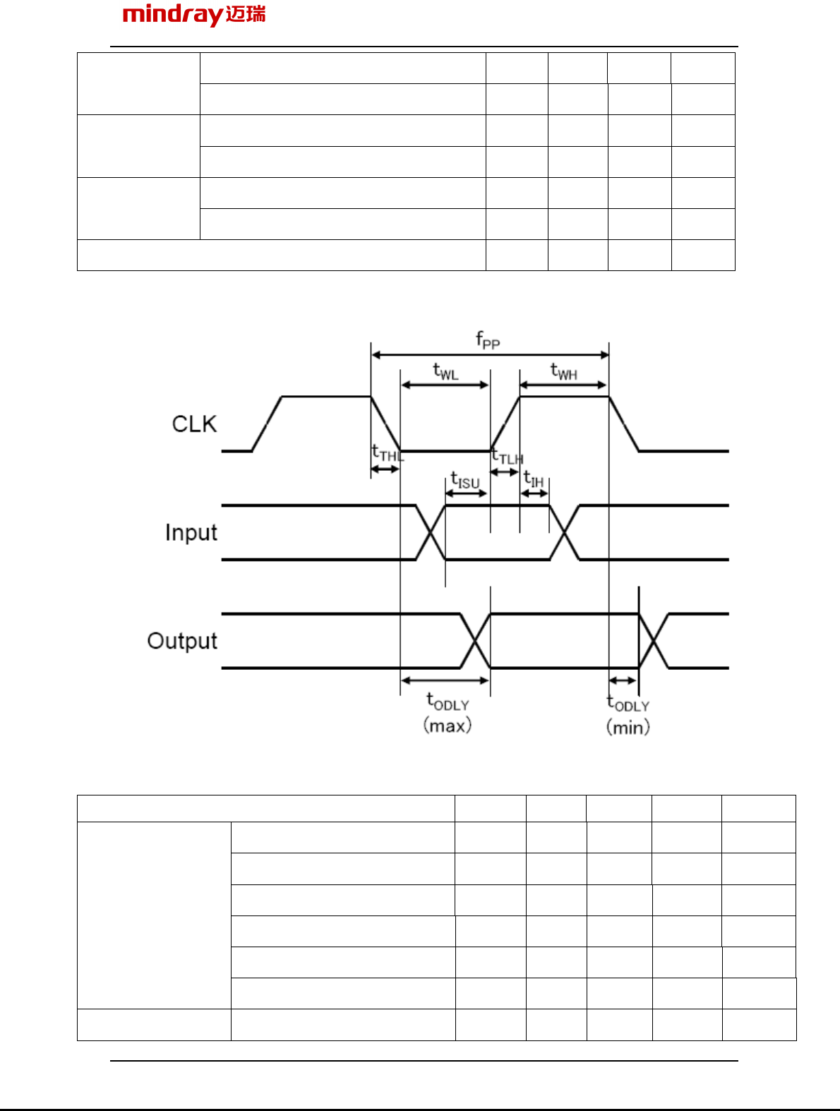
1.7.3.3 WLAN SDIO Timing
1.7.3.3.1 Default Mode
Figure 5 WLAN SDIO Timing, Default Mode
Table 9 WLAN SDIO Timing, Default Mode
Parameter Symbol
Min Typ Max Unit
Frequency-Data Transfer Mode
fPP 0 - 25 MHz
Frequency-Identification Mode fOD 0 - 400- KHz
Clock Low Time tWL 10 - - ns
Clock High Time tWH 10 - - ns
Clock Rise Time tTLH - - 10 ns
Clock CLK (All
values are referred
to min. VIH and max.
VIL)
Min (Vih) = 0.7*VIN
and max (Vil) =
0.2*VIN
Clock Falling Time tTHL - - 10 ns
Inputs: CMD, DAT Input Setup Time tISU 5 - - ns
KF-XXXX-X-XXX-版本
(referenced to CLK) Input Hold Time tIH 5 - - ns
Output Delay time-Data
Transfer Mode
tODLY - - 14 ns
Outputs: CMD, DAT
(referenced to CLK)
Output Delay time-Identification
Mode
tODLY - - 50 ns
Remark: Timing is based on CL < 40pF load on CMD and Data.
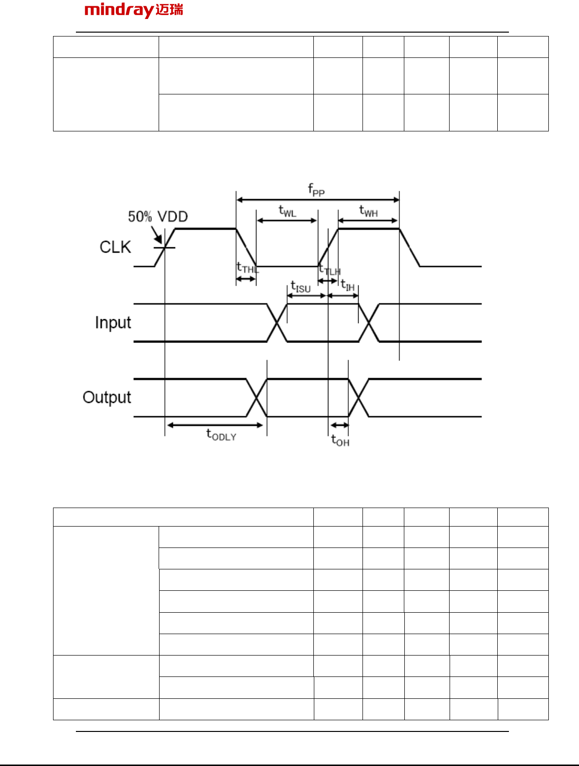
1.7.3.3.2
High Speed Mode
Figure 6 WLAN SDIO Timing, High Speed Mode
Table 10 WLAN SDIO Timing, High Speed Mode
Parameter Symbol
Min Typ Max Unit
Frequency-Data Transfer Mode
fPP 0 - 50 MHz
Frequency-Identification Mode fOD 0 - 400- KHz
Clock Low Time tWL 7 - - ns
Clock High Time tWH 7 - - ns
Clock Rise Time tTLH - - 3 ns
Clock CLK (All
values are referred
to min. VIH and max.
VIL)
Min (Vih) = 0.7*VIN
and max (Vil) =
0.2*VIN
Clock Falling Time tTHL - - 3 ns
Input Setup Time tISU 6 - - ns
Inputs: CMD, DAT
(referenced to CLK) Input Hold Time tIH 2 - - ns
Outputs: CMD, DAT Output Delay time-Data tODLY - - 14 ns
KF-XXXX-X-XXX-版本
Transfer Mode
Output Hold time tOH - - 50 ns
(referenced to CLK)
Total System Capacitance
(each line)
CL - - 40 pF
Remark: Timing is based on CL < 40pF load on CMD and Data.
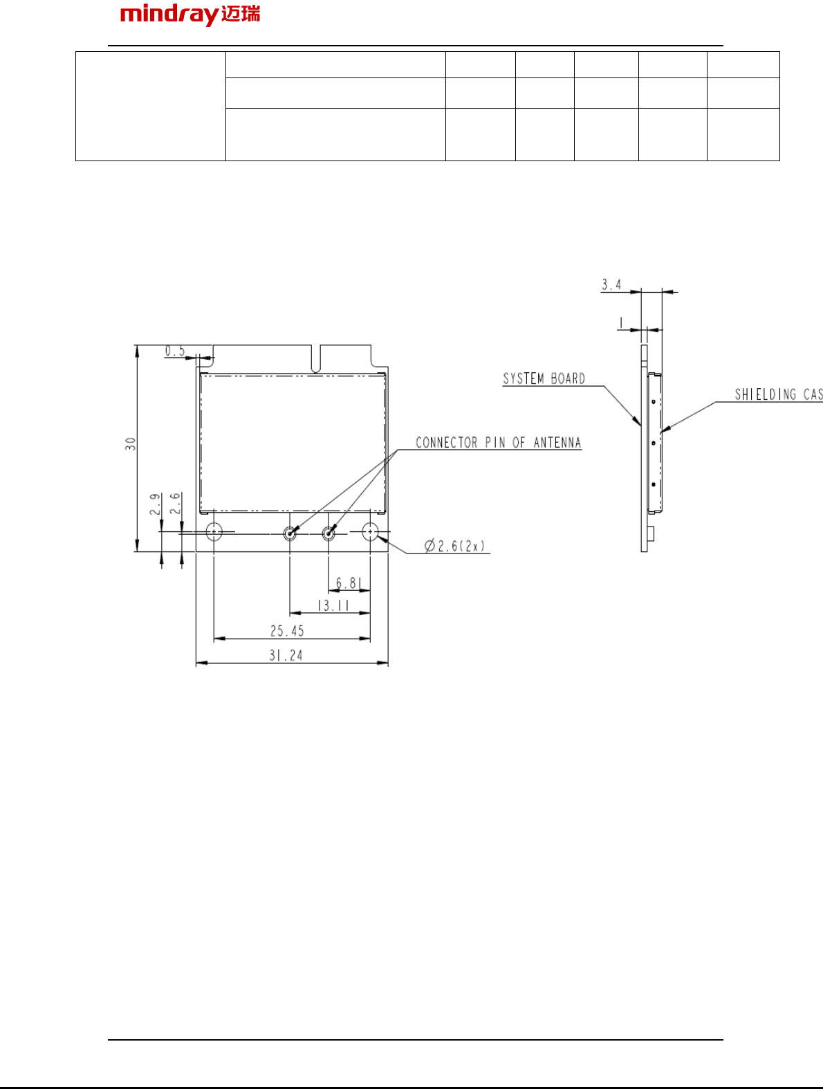
1.7.4 Mechanical
This device complies with Industry Canada licence-exempt RSS standard(s).
Operation is subject to the following two conditions: (1) this device may not cause
interference, and (2) this device must accept any interference, including interference
that may cause undesired operation of the device.
Le présent appareil est conforme aux CNR d'Industrie Canada applicables aux
appareils radio exempts de licence. L'exploitation est autorisée aux deux conditions
suivantes : (1) l'appareil ne doit pas produire de brouillage, et (2) l'utilisateur de
l'appareil doit accepter tout brouillage radioélectrique subi, même si le brouillage est
susceptible d'en compromettre le fonctionnement.
The distance between user and products should be no less than 20cm
La distance entre l'utilisateur et de produits ne devrait pas être inférieure à 20cm
The host device must be labelled to display the IC ID of the module "Contains IC:
9726A-WM1010BGN10"

KF-XXXX-X-XXX-版本
Appendix A FCC
A.1 FCC statement in User's Manual (for class B)
"Federal Communications Commission (FCC) Statement This Equipment has been tested
and found to comply with the limits for a class B digital device, pursuant to Part 15 of the FCC
rules. These limits are designed to provide reasonable protection against harmful interference in a
residential installation. This equipment generates, uses and can radiate radio frequency energy
and, if not installed and used in accordance with the instructions, may cause harmful interference
to radio communications. However, there is no guarantee that interference will not occur in a
particular installation. If this equipment does cause harmful interference to radio or television
reception, which can be determined by turning the equipment off and on, the user is encouraged
to try to correct the interference by one or more of the following measures:
Reorient or relocate the receiving antenna.
Increase the separation between the equipment and receiver.
Connect the equipment into an outlet on a circuit different from that to which the receiver is
connected.
Consult the dealer or an experienced radio/TV technician for help.
A.2 FCC Statements:
1. This device complies with Part 15 of the FCC rules. Operation is subject to the following
two conditions:
This device may not cause harmful interference,
and This device must accept any interference received, including interference that
may cause undesired operation.
2. This device and its antenna(s) must not be co-located or operating in conjunction with
any other antenna or transmitter.
3. Changes or modifications to this unit not expressly approved by the party responsible for
compliance could void the user authority to operate the equipment.
4. This compliance to FCC radiation exposure limits for an uncontrolled environment, the
minimum of 20 cm separation distance shall be maintained between antenna and body.
The host device must be labelled to display the FCC ID of the module "Contains
FCC ID: ZLZWM1010BGN10"