Mitac 8170 Users Manual
8170 to the manual f95a7b09-acb2-4a72-98f2-8a54f26aa8a1
2015-02-09
: Mitac Mitac-8170-Users-Manual-556372 mitac-8170-users-manual-556372 mitac pdf
Open the PDF directly: View PDF ![]() .
.
Page Count: 217 [warning: Documents this large are best viewed by clicking the View PDF Link!]
SERVICE MANUAL FOR
8 1 7 0
8 1 7 08 1 7 0
8 1 7 0
SERVICE MANUAL FOR
SERVICE MANUAL FOR
8 1 7 0
8 1 7 08 1 7 0
8 1 7 0
8 1 7 0
8 1 7 08 1 7 0
8 1 7 0
TESTING TECHNOLOGY DEPARTMENT / TSSC
TESTING TECHNOLOGY DEPARTMENT / TSSC
Feb . 2002
BY: Jacey
Jacey Liu
Liu

1
8170 N/B MAINTENANCE
1. Hardware Engineering Specification--------------------------------------------------------------------------------
CONTENTS
CONTENTS
1.1 Introduction--------------------------------------------------------------------------------------------------------------------------------
1.2 System Architecture----------------------------------------------------------------------------------------------------------------------
1.3 Electrical Characteristic-----------------------------------------------------------------------------------------------------------------
1.4 APPENDIX---------------------------------------------------------------------------------------------------------------------------------
1.5 BIOS Specification------------------------------------------------------------------------------------------------------------------------
2. System Assembly & Disassembly ------------------------------------------------------------------------------------
2.1 System View--------------------------------------------------------------------------------------------------------------------------------
2.2 System Disassembly----------------------------------------------------------------------------------------------------------------------
3. Definition & Location Connectors / Switches Setting -----------------------------------------------------------
3.1 Main Board---------------------------------------------------------------------------------------------------------------------------------
3.2 D/D Board-----------------------------------------------------------------------------------------------------------------------------------
3.3 Touch PAD Board-------------------------------------------------------------------------------------------------------------------------
4. Definition & Location Major Components-------------------------------------------------------------------------
4.1 Main Board---------------------------------------------------------------------------------------------------------------------------------
4.2 D/D Board----------------------------------------------------------------------------------------------------------------------------------
5. Pin Descriptions of Major Components ----------------------------------------------------------------------------
5.1 Pentium 4(Willamette/Northwood) Micro-FCPGA 478 pin----------------------------------------------------------------------
5.2 Intel 82845(Brookdale Memory Controller HUB)----------------------------------------------------------------------------------
5.3 Intel 82801BA(I/O Controller HUB )-------------------------------------------------------------------------------------------------
5.4 PCI4410(PCMCIA/1394 LINK Controller )----------------------------------------------------------------------------------------
4
4
5
22
32
39
82
82
86
104
104
107
108
109
109
111
112
112
118
125
130

2
8170 N/B MAINTENANCE
CONTENTS
CONTENTS
6. System Block Diagram -------------------------------------------------------------------------------------------------
7.1 Introduction--------------------------------------------------------------------------------------------------------------------------------
7.2 Error Codes--------------------------------------------------------------------------------------------------------------------------------
7.3 Debug Card--------------------------------------------------------------------------------------------------------------------------------
7. Maintenance Diagnostic ------------------------------------------------------------------------------------------------
8. Trouble Shooting --------------------------------------------------------------------------------------------------------
8.1 No Power------------------------------------------------------------------------------------------------------------------------------------
8.2 Battery Can not Be Charged-----------------------------------------------------------------------------------------------------------
8.3 No Display----------------------------------------------------------------------------------------------------------------------------------
8.4 VGA Controller Failure LCD No Display-------------------------------------------------------------------------------------------
8.5 VGA Controller Failure External Monitor No Display---------------------------------------------------------------------------
8.6 Memory Test Error-----------------------------------------------------------------------------------------------------------------------
8.7 Keyboard(K/B) and Touch Pad(T/B) Test Error-----------------------------------------------------------------------------------
8.8 Hard Drive Test Error-------------------------------------------------------------------------------------------------------------------
8.9 CD-ROM Drive Test Error-------------------------------------------------------------------------------------------------------------
8.10 USB Port Test Error--------------------------------------------------------------------------------------------------------------------
8.11 PIO Port Test Error---------------------------------------------------------------------------------------------------------------------
8.12 PC-Card Failure-------------------------------------------------------------------------------------------------------------------------
8.13 IEEE1394 Failure-----------------------------------------------------------------------------------------------------------------------
8.14 Audio Failure----------------------------------------------------------------------------------------------------------------------------
8.15 LAN Test Failure------------------------------------------------------------------------------------------------------------------------
9. Spare Parts List ----------------------------------------------------------------------------------------------------------
136
137
137
138
140
142
143
148
151
153
155
157
159
161
163
165
167
169
171
173
176
178

3
8170 N/B MAINTENANCE
CONTENTS
CONTENTS
10. System Explode View -------------------------------------------------------------------------------------------------
11. Circuit Diagram --------------------------------------------------------------------------------------------------------
12. Reference ----------------------------------------------------------------------------------------------------------------
189
190
215
4
8170 N/B MAINTENANCE
1.Hardware Engineering Specification
1.1 Introduction
1.1.1 General Description
This document describes the system hardware engineering specification for 8170 portable notebook computer system.
The 8170 notebook computer is a new mainstream high performance notebook in the MiTAC notebook family.
1.1.2 System Overview
CPU mPGA 478 -PIN Socket Support Intel Pentium (Willamette)/Northwood in mFC-PGA2 package
1. Dual independent Displays(LCD/CRT, LCD/TV,CRT/TV)
2. Support Motion Compensation and iDCT
3. Support Simultaneous display
Momory Two 144Pin SO-DIMM ,withont and on-board Memory
1. Support one slot of TypeII
2. Non Support Zoom video/Audio Function
IDE Support 2 IDE channel,Up to Ultra DMA 100
Support Dual 85MHz LVDS interface.
Support up to QXGA(2048*1536) Resolution
Button 5 Easy Start Button(functions defined by user)& 1 Mail Receive Button
LAN Support to 10/100 Based T
Modem 56Kbps V.90 MDC Modem
Pointing Glide PAD with 2 Buttons and 1 scroll button
Keyboard Internal Key Matrix Keyboard
BIOS 512KB Flash EEPROM (Include System BIOS&VGA BIOS)
Video
PCMCIA
LCD Display
5
8170 N/B MAINTENANCE
Audio 1. AC'97 Interface Codec. Sound Blaster Pro Compatible.
2. Built-In 21W speaker and 1 Mono-Microphone
1. Bi-Direction Parallel Port (EPP/ECP) 2. External VGA Port(D-SUB 15Pins)
3. 2 Standard USB 1.1 Port 4. SPIDF Jack
5. RJ-11 Port for Modem 6. Microphone In Jck
7. RJ-45 Port for LAN 8. VR for Audio Volume Control
9. DC Input Jack 10.Mini IEEE 1394 Port
11. S-Video Output Port(NTSC/PAL) 12. Battery Connector
Suspend Mode POS(S1), Suspend to RAM(S3), Suspend to Disk(S4)
Indicator HDD,FDD,CD-ROM,Num Lock,Caps Lock, Scroll Lock LEDs
I/O Port
1.2 System Architecture
1.2.1 Block Diagram(without Power System)
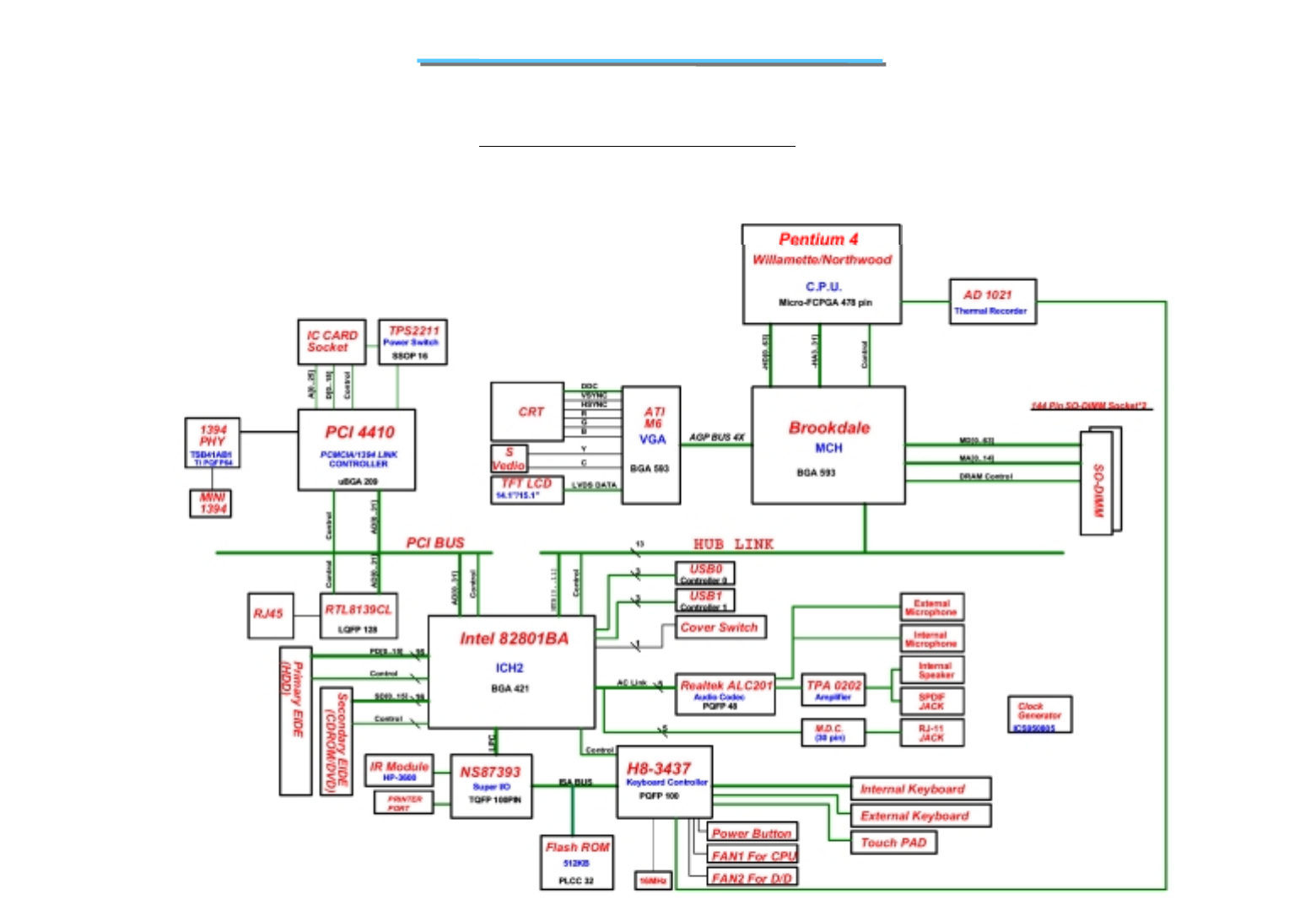
6
8170 N/B MAINTENANCE
8170 System Block Diagram

7
8170 N/B MAINTENANCE
1.2.2 Function Description
Socket Intel Pentium 4/ Northwood processors with 100MHz FSB.400MHz system bus.Capable of mFC-PGA2
package
1.2.2.1 CPU
Available at 1.50, 1.60, 1.70, 1.80, 1.90 and 2 GHz
Binary compatible with applications running on previous members of the Intel microprocessor line
Intel® NetBurst™ micro-architecture
System bus frequency at 400 MHz
Rapid Execution Engine: Arithmetic Logic Units (ALUs) run at twice the processor core frequency
Hyper Pipelined Technology
Advance Dynamic Execution
---Very deep out-of-order execution
---Enhanced branch prediction
Level 1 Execution Trace Cache stores 12K micro-ops and removes decoder latency from main execution loops
8 KB Level 1 data cache
256 KB Advanced Transfer Cache (on-die,full speed Level 2 (L2) cache) with 8-way associatively and Error
Correcting Code (ECC)
144 new Streaming SIMD Extensions 2 (SSE2) instructions
Enhanced floating point and multimedia unit for enhanced video, audio,encryption, and 3D performance
Power Management capabilities
---System Management mode
---Multiple low-power states

8
8170 N/B MAINTENANCE
Optimized for 32-bit applications running on advanced 32-bit operating systems
8-way cache associatively provides improved cache hit rate on load/store operations.
1.2.2.2 CORE LOGIC
Intel Brookdale 82845 Memory Control HUB
Intel® Pentium® 4 Processor (478 pin package) Support:
---Enhanced Mode Scaleable Bus Protocol
---2x Address, 4x Data
---System Bus interrupt delivery
---400 MHz system bus
---System Bus Dynamic Bus Inversion (DBI)
---32-bit system bus addressing
---12 deep In-Order Queue
---AGTL+ bus driver technology with integrated AGTL+ termination resistors
System Memory Support
---Directly supports one SDR SDRAM channel, 64 bits wide (72 bits with ECC)
---133 MHz SDR SDRAM devices
---64 Mb, 128 Mb, 256 Mb and 512 Mb technologies for x8 and x16 devices
---By using 64 Mb technology, the smallest memory capacity possible is 32 MB
---Configurable optional ECC operation (single bit Error Correction and multiple bit Error Detection)
---Page sizes of 2 KB, 4 KB, 8 KB and 16 KB (individually selected for every row)
---Thermal management
---Maximum of 3 Double-Sided DIMMs (6rows populated) with unbuffered PC133 (with or without ECC)
---3 GB Maximum using 512 Mb technology
---Supports up to 24 simultaneous open pages
---Maximum memory bandwidth of 1.067 GB/s with PC133

9
8170 N/B MAINTENANCE
Hub Interface to Intel® 82801BA ICH2
---266 MB/s point-to-point hub interface to ICH2
---66 MHz base clock
---MSI interrupt messages, power management state change, SMI, SCI and SERR error indication
Accelerated Graphics Port (AGP) Interface
--- Supports a single AGP device (either a connector or on the motherboard)
---Supports AGP 2.0 including 1x, 2x, and 4x AGP data transfers and 2x/4x Fast Write protocol
---Supports only 1.5 V AGP electrical characteristics
---32 deep AGP request queue
---Delayed transaction support for AGP-to-System Memory FRAME# semantic reads
System Interrupt Support
---System bus interrupt delivery mechanism
---Interrupts signaled as upstream memory writes from AGP/PCI
---Supports peer MSI between hub interface and AGP
---Provides redirection for IPI and upstream interrupts to the system bus
Power Management
---SMRAM space remapping to A0000h
---Supports extended SMRAM space above 256 MB, additional TSEG from Top of Memory
interface are not supported
---PC ’99 suspend to DRAM support
---ACPI, Revision 1.0b compliant power management
---APM, Revision 1.2 compliant power management
---NT Hardware Design Guide, Version 1.0 compliant
Package
---MCH: 593 pin FC-BGA (37.5 x 37.5 mm)

10
8170 N/B MAINTENANCE
Intel 82801BA Internal Connect HUB
PCI Bus I/F
---Supports PCI at 33 MHz
---Supports PCI Rev 2.2 Specification
---133 MByte/sec maximum throughput
---Supports up to 6 master devices on PCI
---One PCI REQ/GNT pair can be given higher arbitration priority (intended for external 1394 host controller)
Integrated LAN Controller
---WfM 2.0 Compliant
---Interface to discrete LAN Connect component
---10/100 Mbit/sec Ethernet support
---1 Mbit/sec HomePNA* support
Integrated IDE Controller
---Independent timing of up to 4 drives
---Ultra ATA/100/66/33, BMIDE and PIO modes
Read transfers up to 100MB/s, Writes to 89 MB/s
---Separate IDE connections for Primary and Secondary cables
---Implements Write Ping-Pong Buffer for faster write performance
USB
---2 UHCI Host Controllers with a total of 4 ports
---USB 1.1 compliant
---Supports wake-up from sleeping states S1–S4
---Supports legacy Keyboard/Mouse software
AC'97 Link for Audio and Telephony CODECs
---AC’97 2.1 compliant

11
8170 N/B MAINTENANCE
---Independent bus master logic for 5 channels (PCM In/Out, Mic Input, Modem In/Out)
---Separate independent PCI functions for Audio and Modem
---Support for up to six channels of PCM audio output (full AC3 decode)
---Supports wake-up events
Interrupt Controller
---Support up to 8 PCI interrupt pins
---Supports PCI 2.2 Message-Based Interrupts
---Two cascaded 82C59
---Integrated I/O APIC capability
---15 interrupts supported in 8259 mode, 24 supported in I/O APIC mode
---Supports Serial Interrupt Protocol
---Supports Front-Side Bus interrupt delivery
1.8 V operation with 3.3 V I/O
---5V tolerant buffers on IDE, PCI, USB Over current and Legacy signals
GPIO
---TTL, Open-Drain, Inversion
Timers Based on 82C54
---System timer, Refresh request, Speaker tone output
Power Management Logic
---ACPI 1.0 compliant
---ACPI Power Management Timer
---PCI PME# support
---SMI# generation
---All registers readable/restorable for proper resume from 0V suspend states
---Support for APM-based legacy power management for non-ACPI implementations

12
8170 N/B MAINTENANCE
External Glue Integration
---Integrated Pull-up, Pull-down and Series Termination resistors on IDE and processor interface
Enhanced Hub I/F buffers improve routing flexibility (Not available with all Memory Controller Hubs)
Firmware Hub (FWH) I/F supports BIOS memory size up to 8 MBs
Low Pin count (LPC) I/F
---Allows connection of legacy ISA and X-Bus devices such as Super I/O
---Supports two Master/DMA devices.
Enhanced DMA Controller
---Two cascaded 8237 DMA controllers
---PCI DMA: Supports PC/PCI — Includes two PC/PCI REQ#/GNT# pairs
---Supports LPC DMA
---Supports DMA Collection Buffer to provide Type-F DMA performance for all DMA channels
Real-Time Clock
---256-byte battery-backed CMOS RAM
---Hardware implementation to indicate century rollover
System TCO Reduction Circuits
---Timers to generate SMI# and Reset upon detection of system hang
---Timers to detect improper processor reset
---Integrated processor frequency strap logic
SM Bus
---Host interface allows processor to communicate via SM Bus
---Slave interface allows an external Micro controller to access system resources
---Compatible with most 2-Wire components that are also I2C compatible
13
8170 N/B MAINTENANCE
Supports ISA bus via external PCI-ISA Bridge
360-pin EBGA package
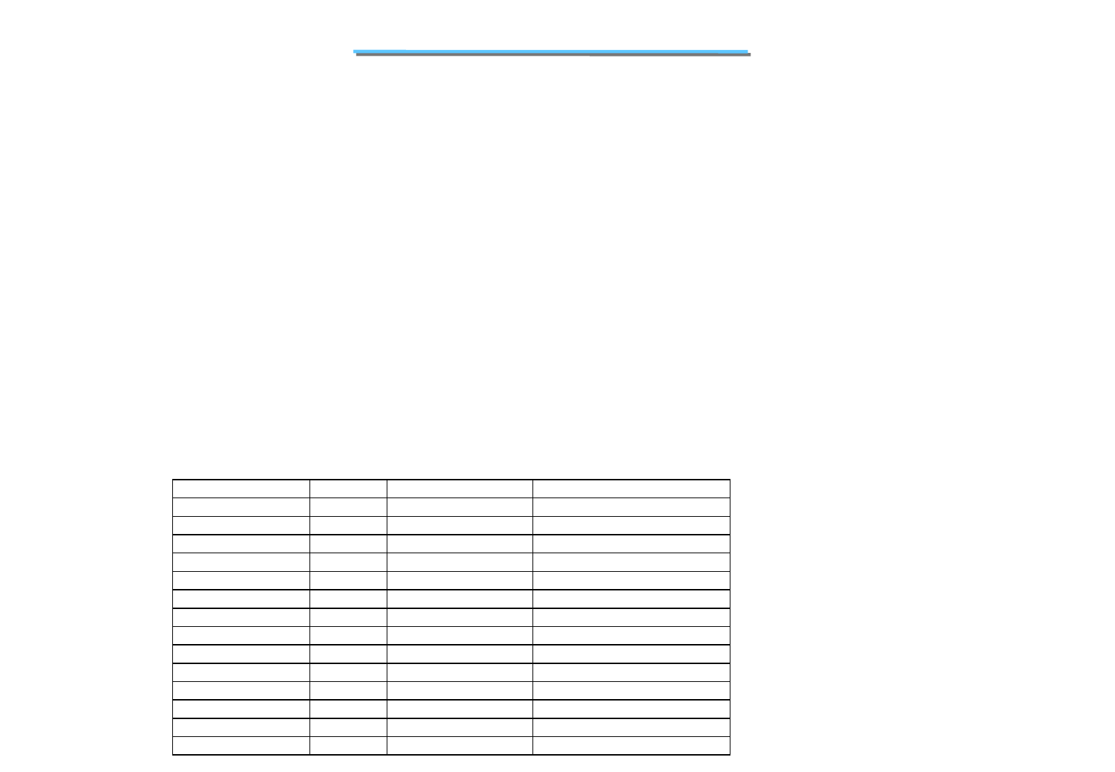
1.2.2.3 Memory
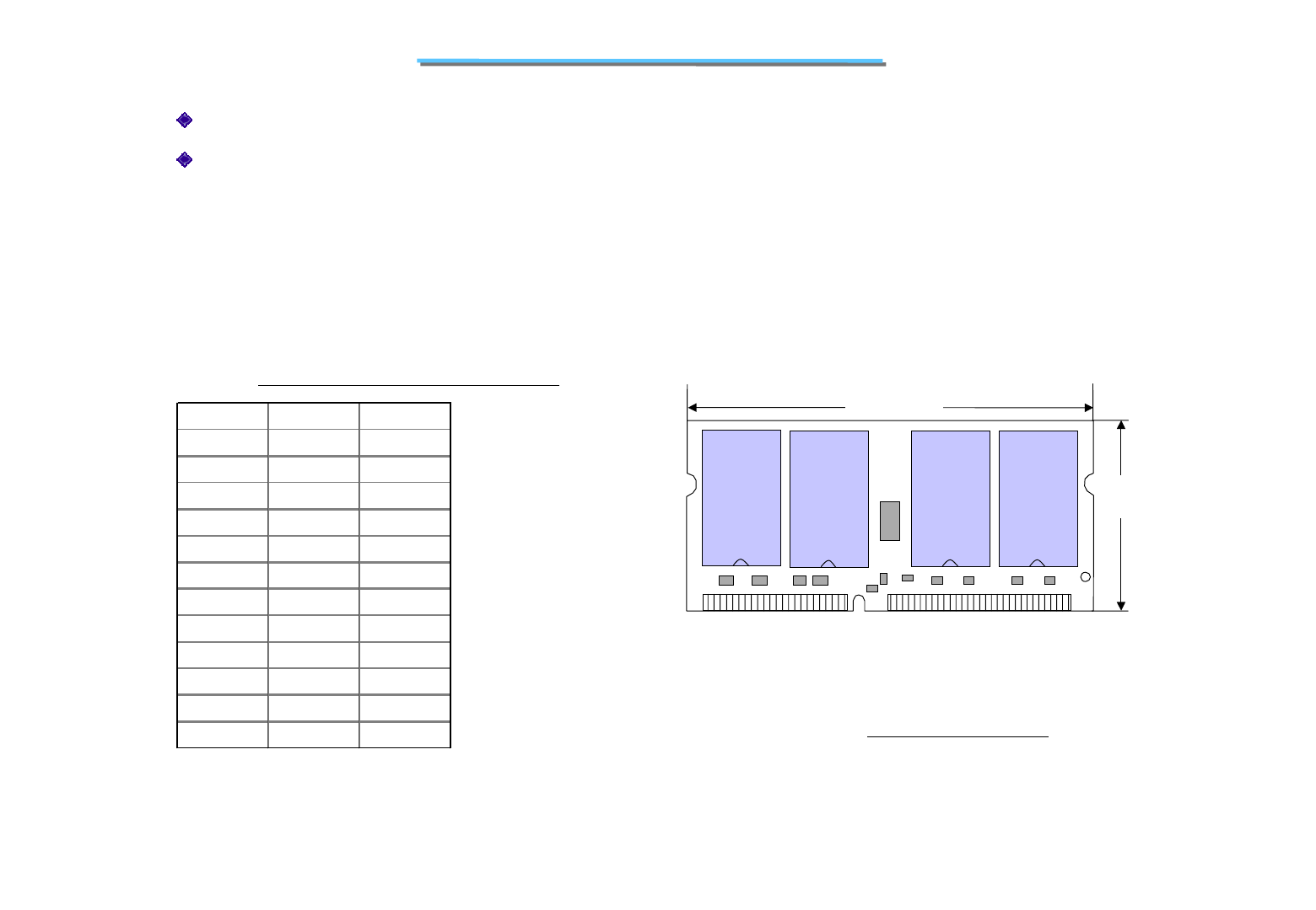
64MB PC133 SDRAM SO-DIMM Expandable to 1024MB(2 SODIMM slots).
Support 3.3V PC133 SDR SDRAM only.
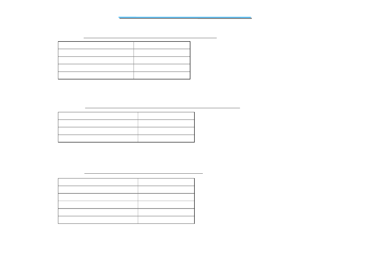
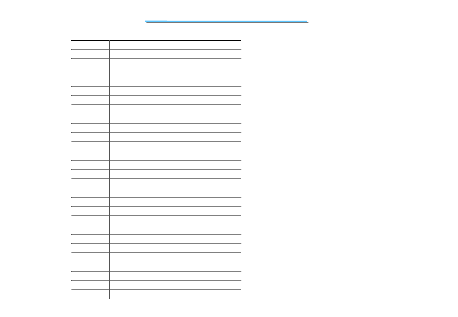
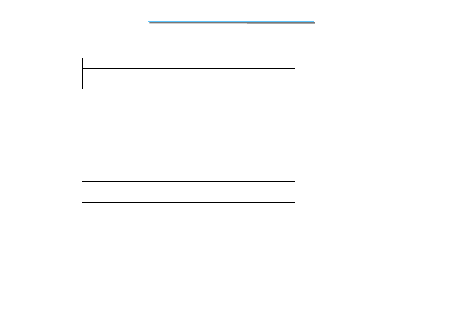
Table 1.1 MEMORY EXPANSION CAPACITY
Slot1 Slot2 Total
64MB 064MB
64MB 32MB 96MB
64MB 64MB 128MB
64MB 128MB 192MB
64MB 256MB 320MB
64MB 512MB 576MB
128MB 128MB 256MB
128MB 256MB 384MB
128MB 512MB 640MB
256MB 256MB 512MB
256MB 512MB 768MB
512MB 512MB 1024MB
Figure 1.1 SO-DIMM MODULE
59 61
54 pin or
50 pin
TSOP
54 pin or
50 pin
TSOP
54 pin or
50 pin
TSOP
54 pin or
50 pin
TSOP
1143
67.6mm ( 2.66”)
SPD
31.75mm
(1.25”)
14
8170 N/B MAINTENANCE
1.2.2.4 I/O Ports
•CRT Port
@ Standard VGA compatible port
@ DDC1 and DDC2B compliant
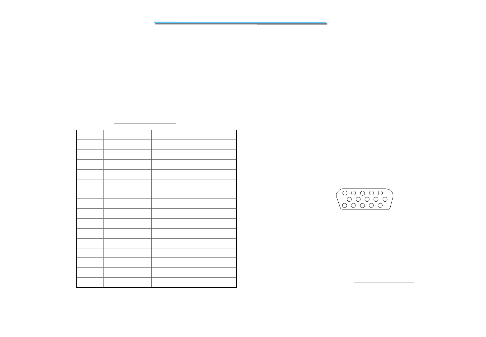
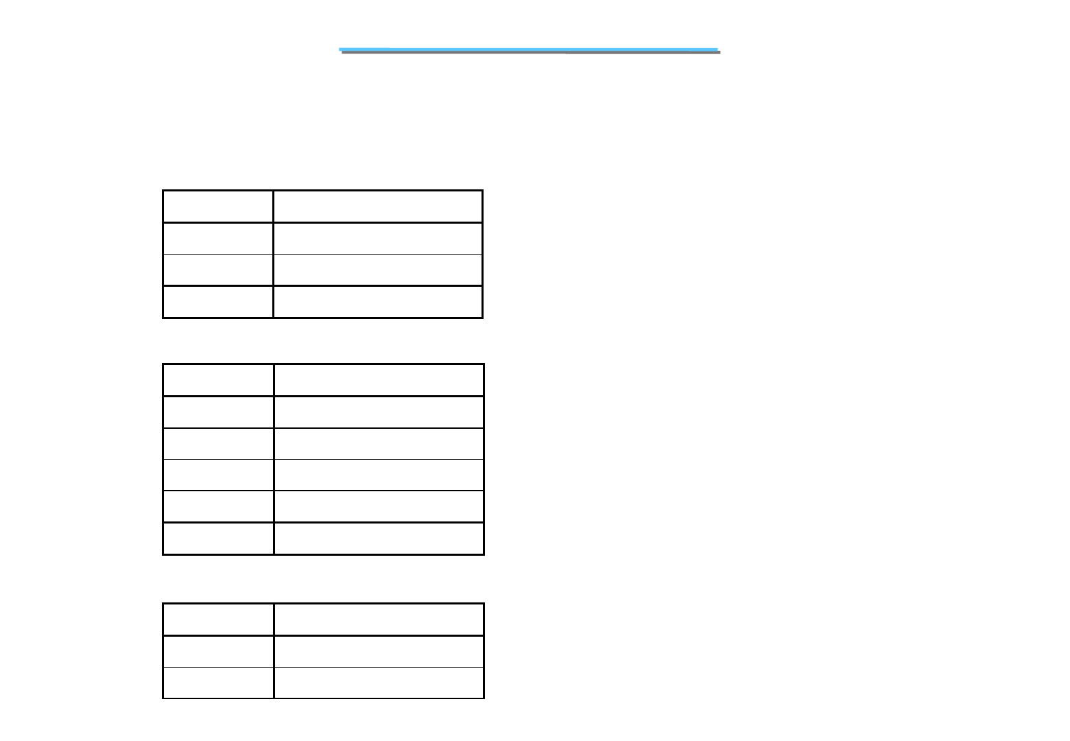
Table 1.2 CRT CONNECTOR
Figure 1.2 CRT CONNECTOR
PIN SIGNAL DESCRIPTION
1RED Red analog video output
2GREEN Green analog video output
3BLUE Blue analog video output
4Monitor Sense Monitor Sense
5GND Ground
6GND Ground
7GND Ground
8GND Ground
9VCC +5VDC
10 GND Ground
11 Monitor Sense Monitor Sense
12 CRT DATA Data from DDC monitor
13 HSYNC Horizontal Sync Control
14 VSYNC Vertical Sync control
15 CRT CLK Clock to DDC monitor
12345
10 6
1112131415
15
8170 N/B MAINTENANCE
Table 1.3 S-VIDEO CONNECTOR
•Standard 4 Pins S-VIDEO Port for TV-Out
@ Support 1024*768 resolution
@ Support 848*480 resolution in 16:9 mode
@ Support PAL and NTSC system
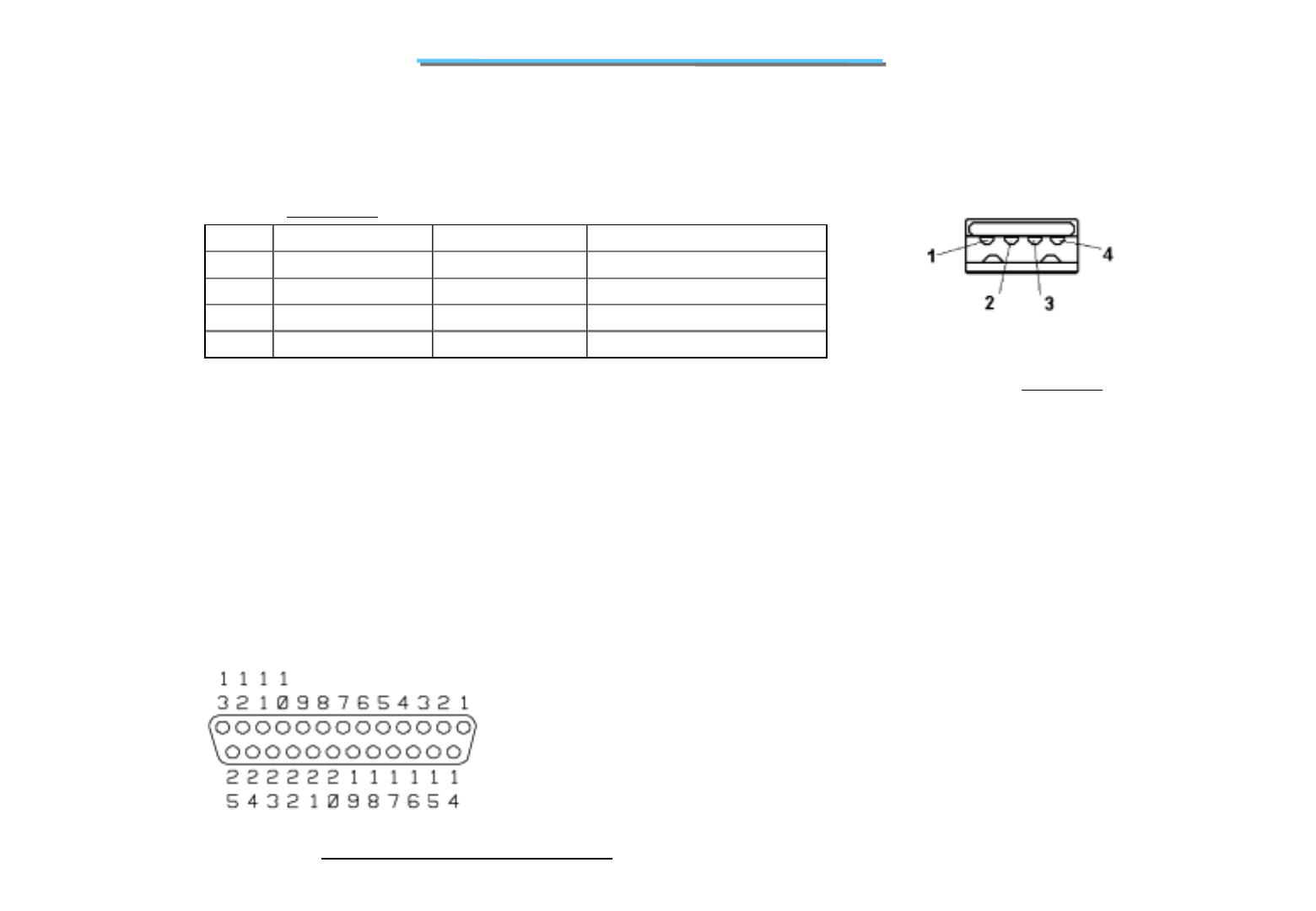
•IEEE1394 Port
Table 1.4 IEEE1394 CONNECTOR
Figure1.4 IEEE1394 Port
•AUDIO Ports
@ Built in 1 mono microphone
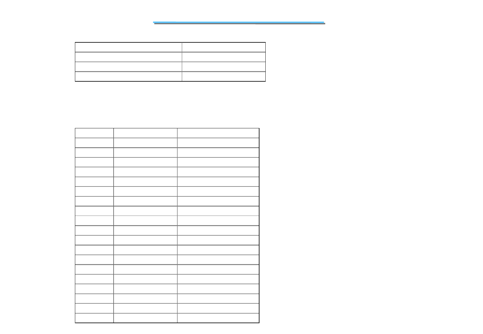
PIN SIGNAL DESCRIPTION
1GND -
2GND -
3LUMA O
4CRMA O
PIN SIGNAL DESCRIPTION
1TPB- I/O
2TPB+ I/O
3TPA- I/O
4TPA+ I/O
Figure1.3 S-VIDEO Port
Pin 1
16
8170 N/B MAINTENANCE
@ Microphone In
•RJ11
@ Connection to Modem Daughter Board connector
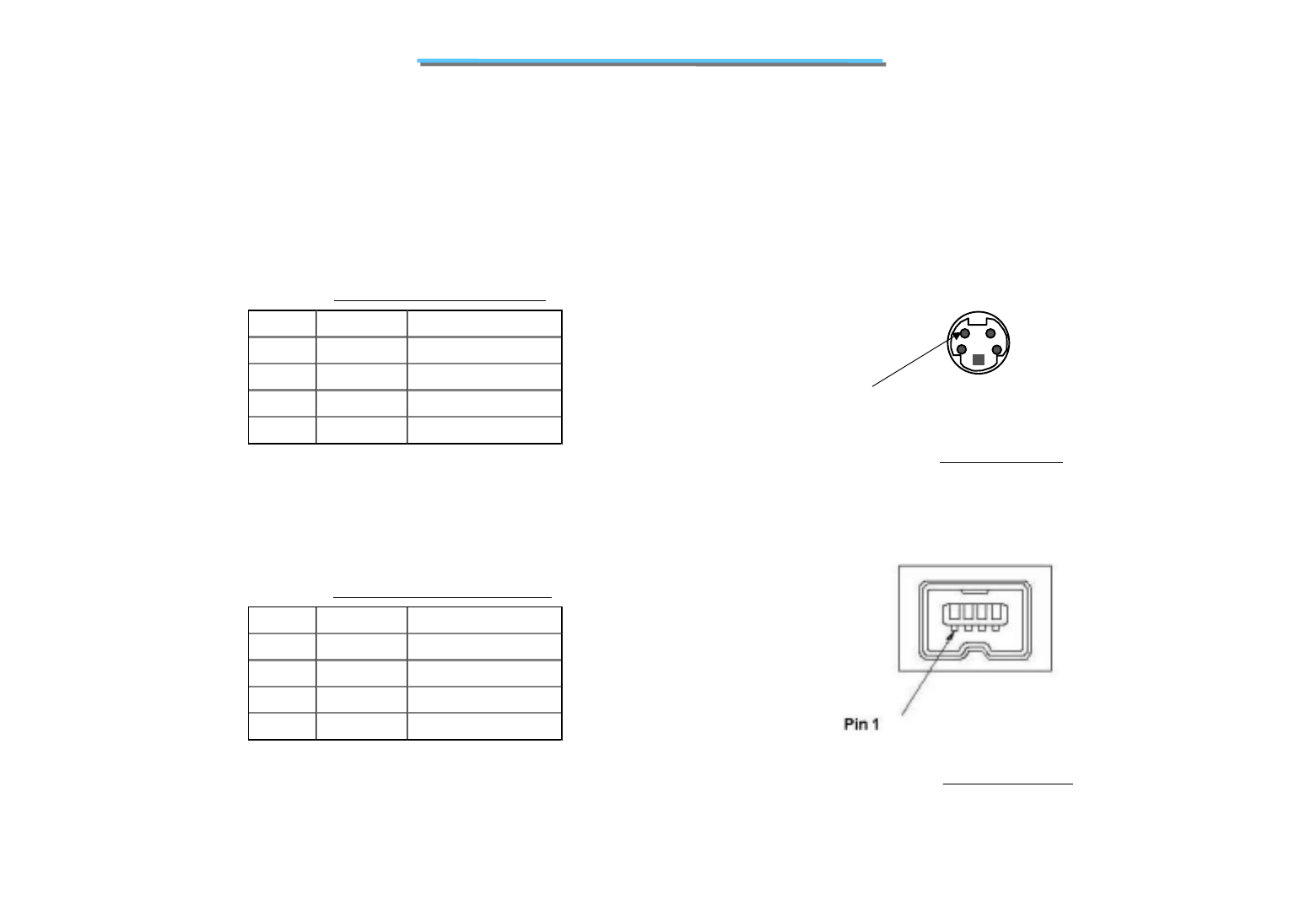
Table 1.5 MODEM CONNECTOR
Figure 1.5 MODEM Port
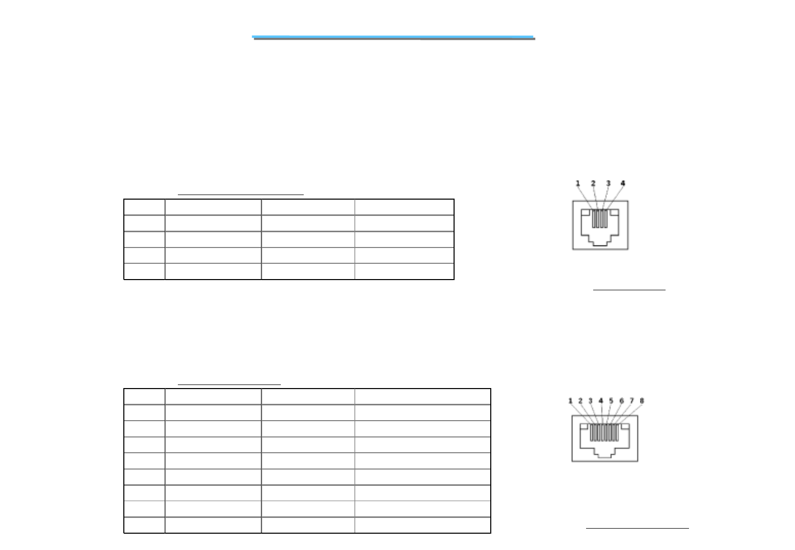
•RJ45
@ Connection to on-board NIC controller
Table 1.6 LAN CONNECTOR
Figure 1.6 LAN CONNECTOR
@ SPDIF
PIN SIGNAL NAME DIRECTION DESCRIPTION
1 NC - No Connect
2 LINE+ I/O Phone Line Positive
3 LINE- I/O Phone Line Negative
4 NC - No Connect
PIN SIGNAL NAME DIRECTION DESCRIPTION
1 TX+ Out Transmit Data Ring
2 TX- Out Transmit Data Tip
3 RX+ IN Receive Data Ring
4 TERM 1 - Internal termination resistor
5 TEMR 2 - Internal termination resistor
6RX IN Receive Data Tip
7 TERM 3 - Internal termination resistor
8 TERM 4 - Internal termination resistor
17
8170 N/B MAINTENANCE
•USB Port
@ Two industry standard USB 1.1 ports
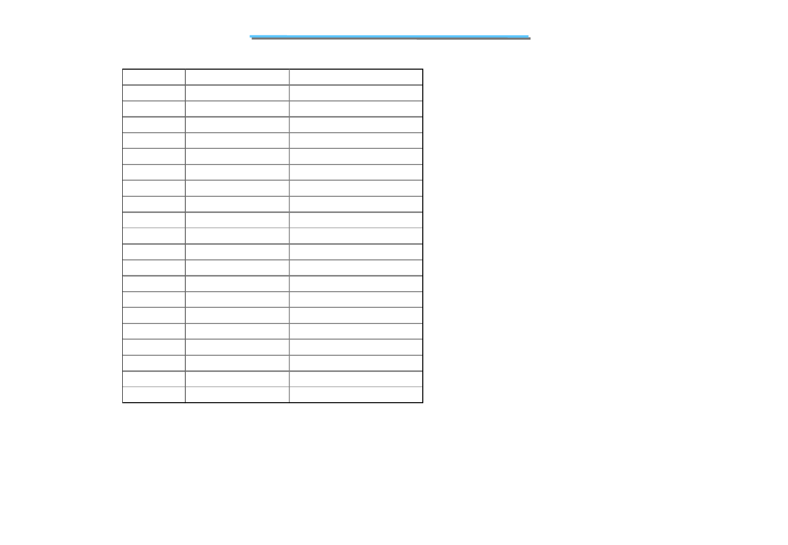
Figure 1.8 PARALLEL PORT CONNECTOR
Table 1.7 USB Port2
Figure 1.7 USB Port
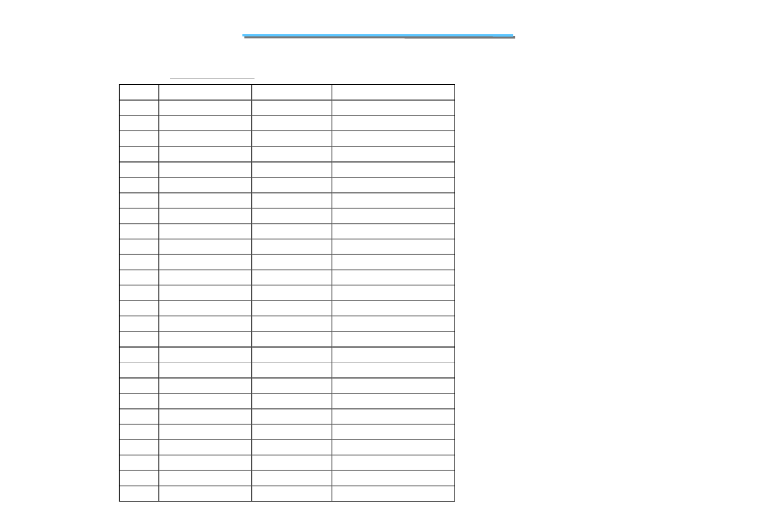
•Parallel Port
@ Configurable as logical ports LPT1,LPT2 or LPT3
@ EPP rev 1.7 & 1.9 compatible
@ ECP(IEEE 1284) compatible
@ Industry standard 25 Pins connector
PIN SIGNAL NAME DIRECTION DESCRIPTION
1 VCC - USB Device Power (+5VDC)
2 DATA- I/O Balanced Data Negaitve
3 DATA+ I/O Balanced Data Posiitve
4GND - Ground
18
8170 N/B MAINTENANCE
Table 1.8 PARALLEL Port
PIN SIGNAL NAME DIRECTION DESCRIPTION
1 STROBE# O Data Strobe
2 PD0 I/O PP Data bit 0
3 PD1 I/O PP Data bit 1
4 PD2 I/O PP Data bit 2
5 PD3 I/O PP Data bit 3
6 PD4 I/O PP Data bit 4
7 PD5 I/O PP Data bit 5
8 PD6 I/O PP Data bit 6
9 PD7 I/O PP Data bit 7
10 -ACK I Printer Acknowledge
11 BUSY I Printer Busy
12 PE I Paper Out
13 SLCT I Print Select Acknowledge
14 -AUTOFDXT O Auto Line Feed
15 -ERROR I Printer Error
16 -INIT O Reset Printer
17 SLCTIN# I Select In
18 GND - Ground
19 GND - Ground
20 GND - Ground
21 GND - Ground
22 GND - Ground
23 GND - Ground
24 GND Ground
25 GND - Ground
Case GND - Ground

19
8170 N/B MAINTENANCE
1.2.2.5 PC CARD SLOT
One Type II/I slot supporting the 1997 PC Card standard, and including full R2(16-bit) and 32-bit Card
bus Data transfer
TI PCI4410(PCMXCIA Controller)& TI TPS2211(Power Switch)
1.2.2.6 GRAPHICAL SUBBSYSTEM
ATI Mobility M6 graphical controller embedded 8M DDR SDRAM
1.2.2.7 DISPLAY
Internal LCD Display is 14.1” TFT ISP XGA color
External Video refresh rate of up to 100HZ support
---Vertical refresh frequencies to meet VESA requirements
---Simultaneous video in specified video modes-switchable with hot key
1.2.2.8 READ ONLY MEMORY(BIOS FLASH)
Fully compatible with industry standard software including windows 2000 & Windows XP
Fully support APM V1.2 and latest ACPI specification
4Mb Flash BIOS
Inside BIOS core
1.2.2.9 POWER MANAGEMENT FEATURES
Local standby mode(individual device such as HDD, graphics controller,LCD etc..)

20
8170 N/B MAINTENANCE
1.2.2.10 KEYBOARD CONTROLLER
Fully APM V1.2 compliant
Fully ACPI V1.1 compliant
Hibernate for Windows 2000 and windows XP
Thermal management
Fully US EPA Energy start compliant
Hitachi H8-3437S
1.2.2.11 SUPER I/O
Ns PC87393F LPC interface Ultra I/O
1.2.2.12 LEDS INDICATOR
CDROM & HDD & NUM & CAP & SCROLL & EMIAL
1.2.2.13 BUTTONS
EMAIL BIN & FIVE PIECE EASY START RTN
CPU Idle mode(including ACPI modes C1 and C2)
Suspend mode(including S1 and S3 ACPI modes)
21
8170 N/B MAINTENANCE
Table 1.9 MODEM DAUGHTER BOARD CONNECTOR
1.2.2.14 MODEM
PIN SIGNAL NAME PIN SIGNAL NAME
1 MONO_OUT 2 NC
3 GND 4 MODEM_SPK
5NC6NC
7NC8GND
9NC10+5V
11 NC 12 NC
13 NC 14 NC
15 GND 16 Pull Up to +3V
17 +3V 18 +5V
19 GND 20 GND
21 +3V 22 ACSYNC
23 ACSDOUT 24 MSDIN
25 -ACRST 26 MSDIN
27 GND 28 GND
29 GND 30 ACBITCLK
22
8170 N/B MAINTENANCE
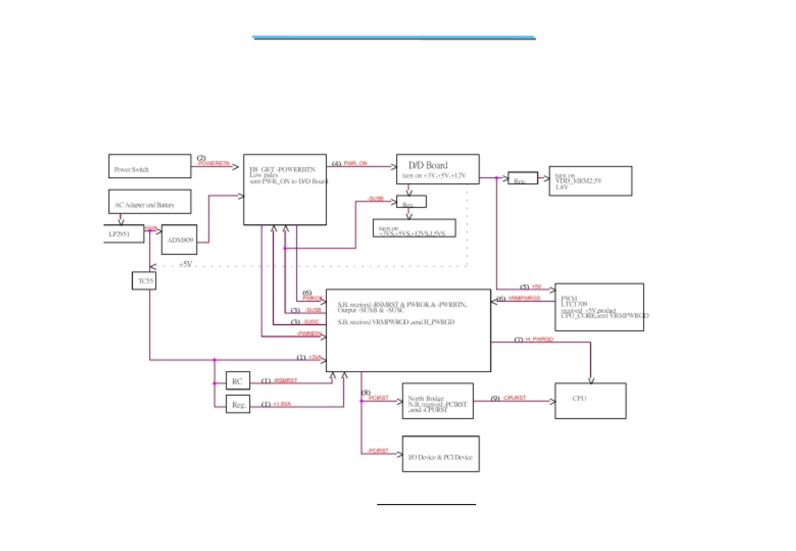
Figure 1.9 Power on Sequence
1.3 Electrical Characteristic
1.3.1 Power On Sequence
23
8170 N/B MAINTENANCE
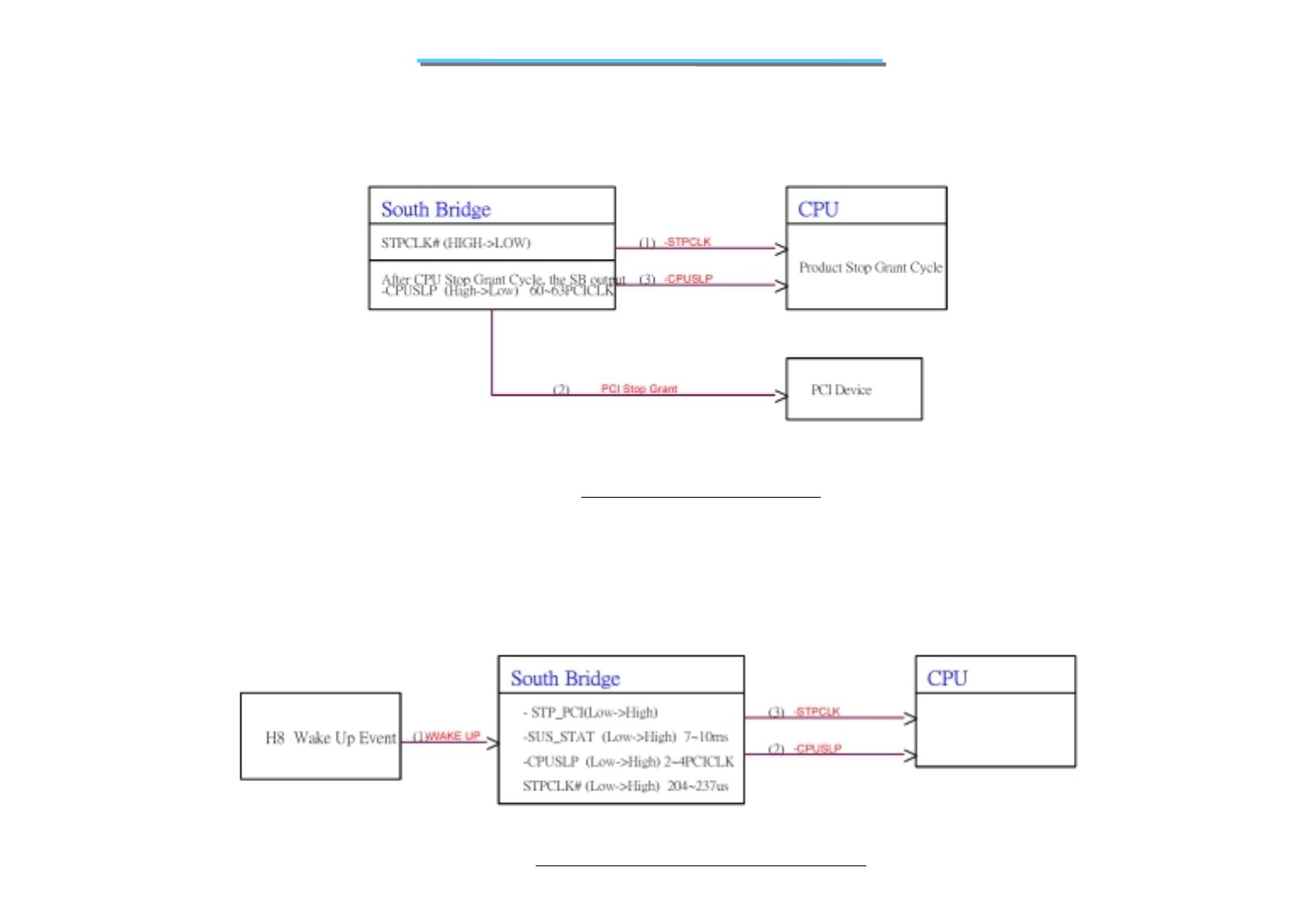
Figure 1.10 Power on Suspend Sequence
1.3.3 Resume from Power Suspend Sequence
Figure 1.11 Resume from Power Suspend Sequence
1.3.2 Power On Suspend Sequence
24
8170 N/B MAINTENANCE
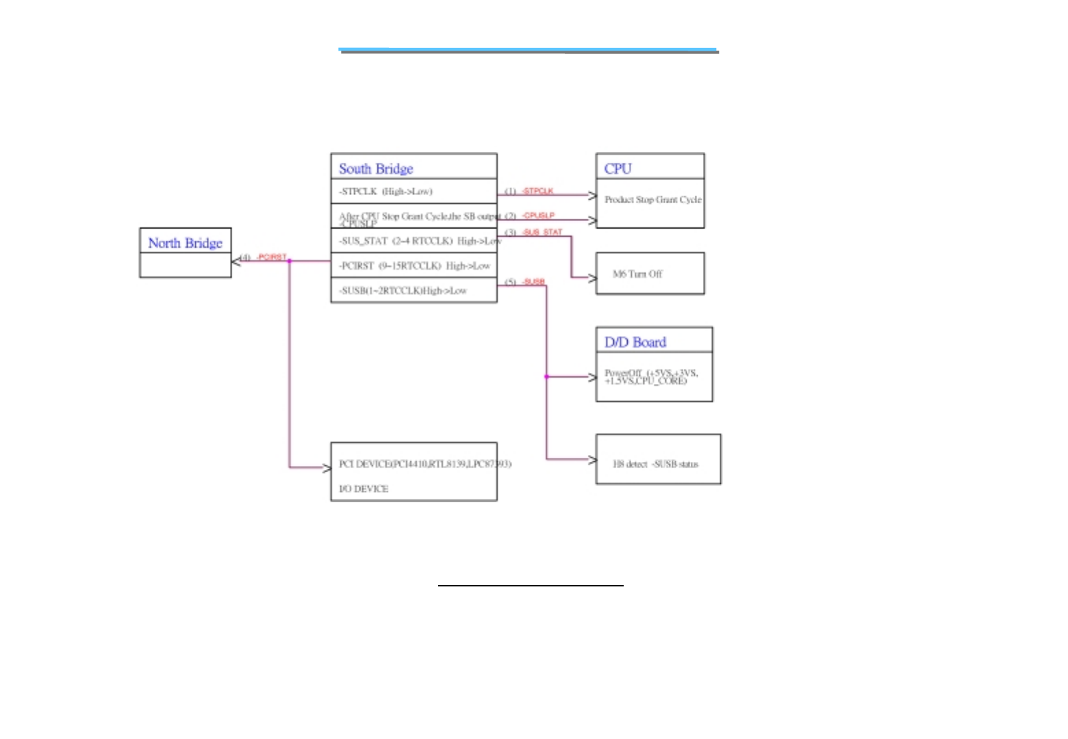
Figure 1.12 Suspend to RAM sequence
1.3.4 Suspend to RAM Sequence
25
8170 N/B MAINTENANCE
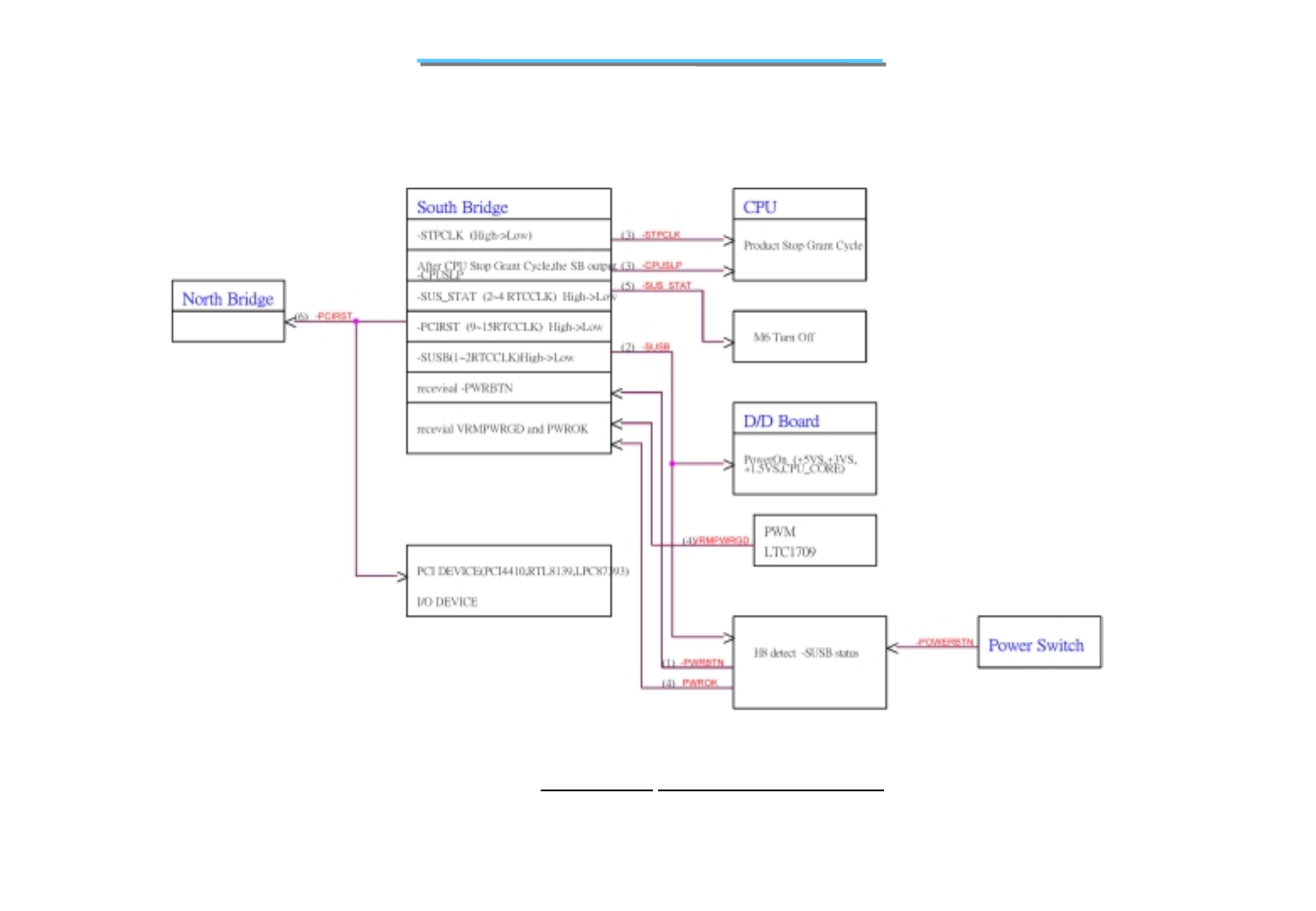
Figure 1.13 Resume from Suspend to RAM Sequence
1.3.5 Resume from Suspend to RAM Sequence
26
8170 N/B MAINTENANCE
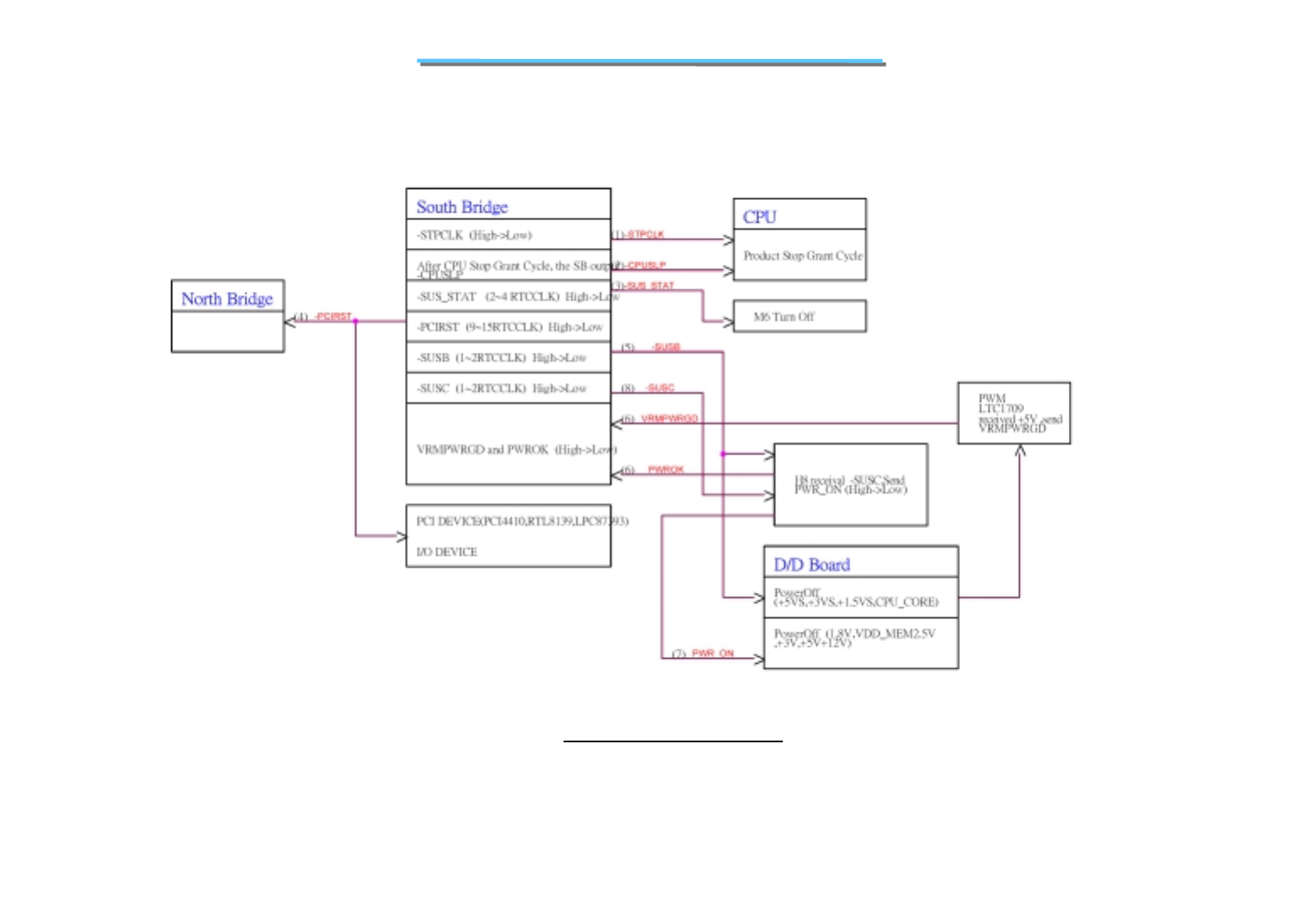
Figure 1.14 Suspend to Disk Sequence
1.3.6 Suspend to Disk Sequence
27
8170 N/B MAINTENANCE
Figure 1.15 Resume from Suspend to Disk Sequence
1.3.7 Resume from Suspend to Disk Sequence
28
8170 N/B MAINTENANCE
1.3.8 ICH2 GPI/O Pin Define
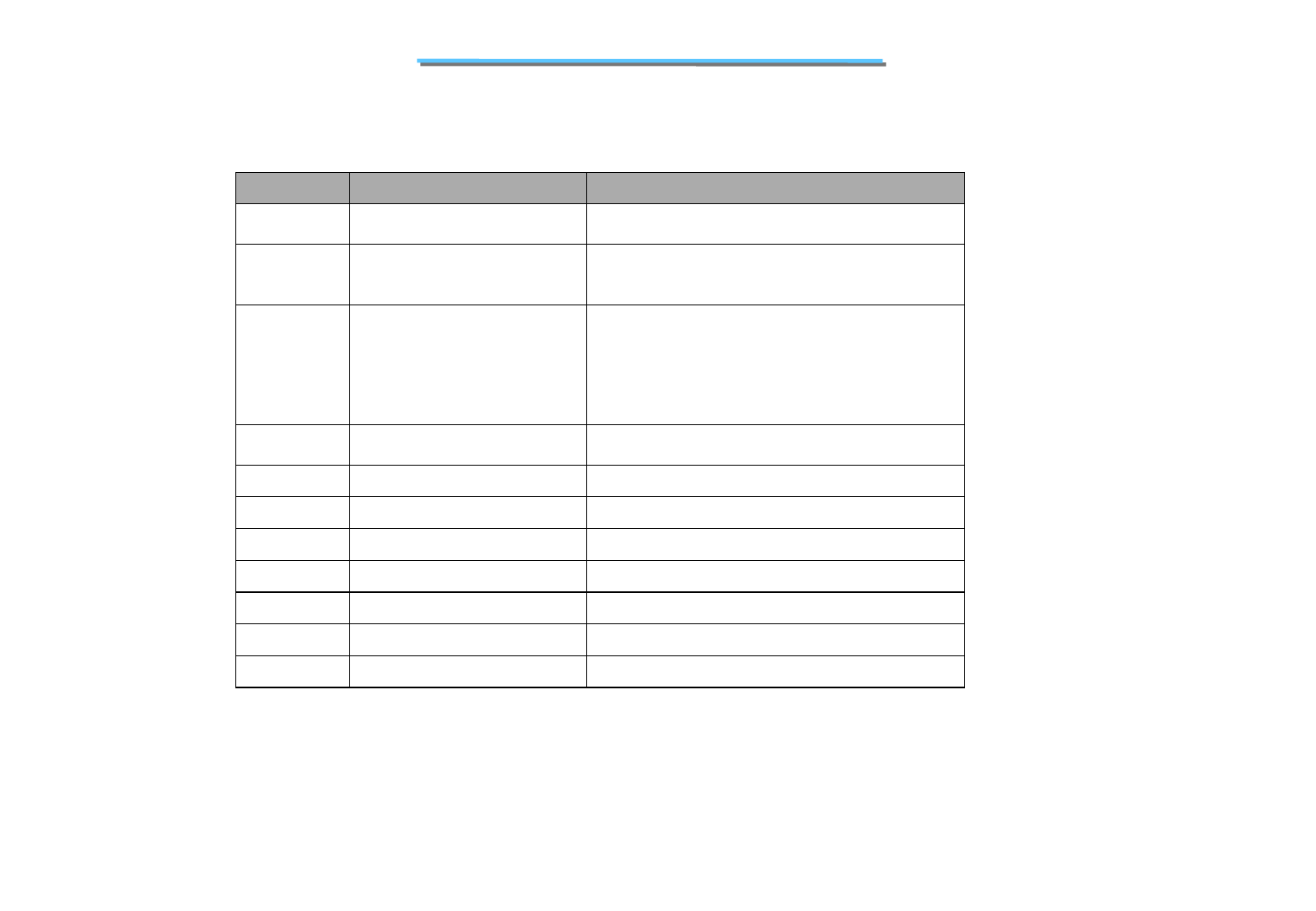
Pin Name Signal Name Power Type During
PCIRST#
Immediately After
PCIRST#
S1 S3 S4/S5 Description
GPIO0 PULL-UP +3.3VS I PC/ P CI DEVICE DRIVEN
GPIO1 PULL-UP +3.3VS I PC/ P CI DEVICE DRIVEN
GPIO2 PULL-UP +3.3VS X X X X X X X
GPIO3 PULL-UP +3.3VS I HIGH-Z HIGH-Z HIGH-Z
GPIO4 PULL-UP +3.3VS I HIGH-Z HIGH-Z HIGH-Z
GPIO6 PULL-UP +3.3VS I M A IN I/ O
GPIO7 PULL-UP +3.3VS I
GPIO8 -SCI +3.3VA I ACPIMODE-SCI
GPIO11 PULL-UP +3.3VA I HIGH-Z HIGH-Z DEFINED DEFINED DEFINED
GPIO12 -EXTSMI +3.3VA I DOS MODE -SMI
GPIO13 PULL-UP +3.3VA I
GPIO1
6
TP +3.3VS O HIGH-Z HI HI OFF OFF
GPIO17 PULL-UP +3.3VS O HIGH-Z HI HI OFF OFF
GPIO18 PULL-UP +3.3VS O HI DEFINED OFF OFF
GPIO19 -ENABKL_MAS
K
+3.3VS O HI HI DEFINED OFF OFF MA SK ENA BL
E
GPIO2
0
-CDROM_PWRON +3.3VS O HI HI DEFINED OFF OFF Control CDROM Power on
GPIO21 -HDD_PWRON +3.3VS O HI HI DEFINED OFF OFF Control HDD Power on
GPIO22 DRAMENA +3.3VS O HIGH-Z HIGH-Z DEFINED OFF OFF DRAM Data select
GPIO23 PULL-UP +3.3VS OD LOW LOW DEFINED OFF OFF
GPIO24 -1394WR +3.3VA O HIGH-Z HI DEFINED DEFINED DEFINED 1394EEPROM R/W
GPIO25 -PCIRST_MSK +3.3VA O HIGH-Z HI DEFINED DEFINED DEFINED MASK PCIRST
GPIO27 -GATE1394 +3.3VA O HIGH-Z HI DEFINED DEFINED DEFINED RST CARD BOARD
GPIO28 SPK_OFF +3.3VA O HIGH-Z HI DEFINED DEFINED DEFINED OFF SPEAKER
29
8170 N/B MAINTENANCE
1.3.9 Power Consumption Of Suspend Mode
Suspend To RAM<TBD
Suspend To Disk/Soft-Off/Mechanical Off<TBD
1.3.10 Clock Harmonic List
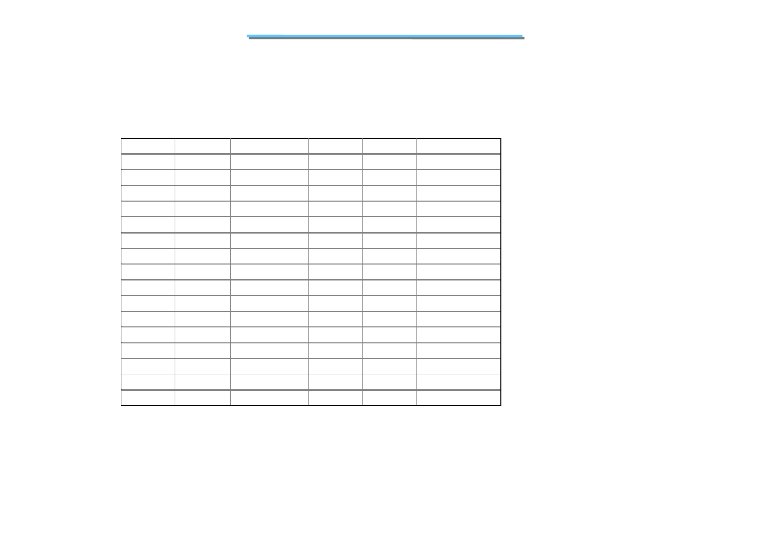
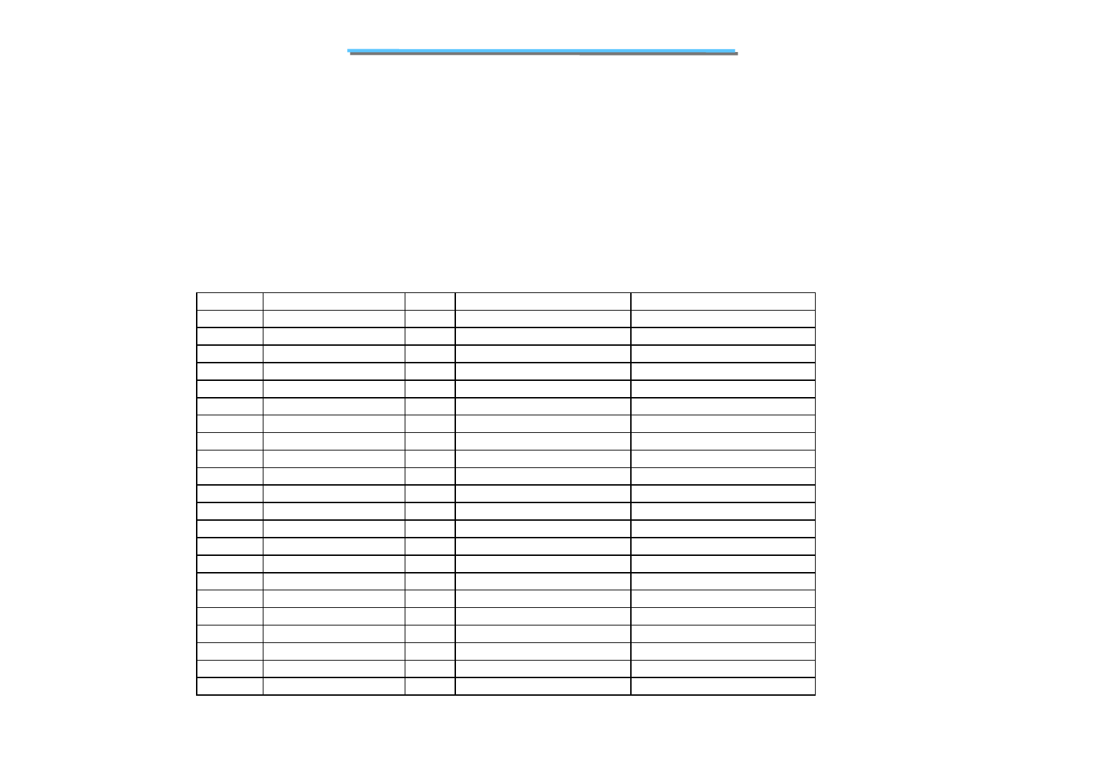
12.288 14.318 16 24 24.576 25 27 32.758 33 48 65 66 100 133
112.288 14.318 16 24 24.576 25 27 32.758 33 48 65 66 100 133
224.576 28.636 32 48 49.152 50 54 65.516 66 96 130 132 200 266
336.864 42.954 48 72 73.728 75 81 98.274 99 144 195 198 300 399
449.152 57.272 64 96 98.304 100 108 131.032 132 192 260 264 400 532
561.44 71.59 80 120 122.88 125 135 163.79 165 240 325 330 500 665
673.728 85.908 96 144 147.456 150 162 196.548 198 288 390 396 600 798
786.016 100.226 112 168 172.032 175 189 229.306 231 336 455 462 700 931
898.304 114.544 128 192 196.608 200 216 262.064 264 384 520 528 800 1064
9110.592 128.862 144 216 221.184 225 243 294.822 297 432 585 594 900 1197
10 122.88 143.18 160 240 245.76 250 270 327.58 330 480 650 660 1000 1330
11 135.168 157.498 176 264 270.336 275 297 360.338 363 528 715 726 1100 1463
12 147.456 171.816 192 288 294.912 300 324 393.096 396 576 780 792 1200 1596
13 159.744 186.134 208 312 319.488 325 351 425.854 429 624 845 858 1300 1729
14 172.032 200.452 224 336 344.064 350 378 458.612 462 672 910 924 1400 1862
15 184.32 214.77 240 360 368.64 375 405 491.37 495 720 975 990 1500 1995
16 196.608 229.088 256 384 393.216 400 432 524.128 528 768 1040 1056 1600 2128
17 208.896 243.406 272 408 417.792 425 459 556.886 561 816 1105 1122 1700 2261
18 221.184 257.724 288 432 442.368 450 486 589.644 594 864 1170 1188 1800 2394
19 233.472 272.042 304 456 466.944 475 513 622.402 627 912 1235 1254 1900 2527
20 245.76 286.36 320 480 491.52 500 540 655.16 660 960 1300 1320 2000 2660
21 258.048 300.678 336 504 516.096 525 567 687.918 693 1008 1365 1386 2100 2793
22 270.336 314.996 352 528 540.672 550 594 720.676 726 1056 1430 1452 2200 2926
23 282.624 329.314 368 552 565.248 575 621 753.434 759 1104 1495 1518 2300 3059
24 294.912 343.632 384 576 589.824 600 648 786.192 792 1152 1560 1584 2400 3192
25 307.2 357.95 400 600 614.4 625 675 818.95 825 1200 1625 1650 2500 3325
Unit: M
Clock Harmonic
30
8170 N/B MAINTENANCE
1.3.11 Audio Performance
8170 meet all the following items.
Table 1.10 Digital Playback (PC-D-A) for line Output
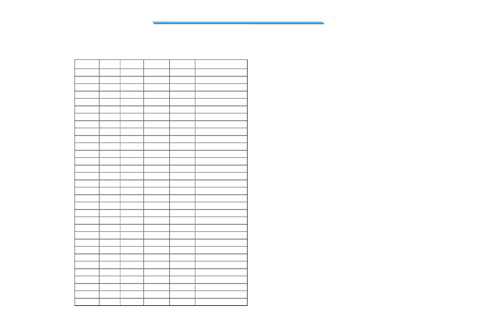
26 319.488 372.268 416 624 638.976 650 702 851.708 858 1248 1690 1716 2600 3458
27 331.776 386.586 432 648 663.552 675 729 884.466 891 1296 1755 1782 2700 3591
28 344.064 400.904 448 672 688.128 700 756 917.224 924 1344 1820 1848 2800 3724
29 356.352 415.222 464 696 712.704 725 783 949.982 957 1392 1885 1914 2900 3857
30 368.64 429.54 480 720 737.28 750 810 982.74 990 1440 1950 1980 3000 3990
31 380.928 443.858 496 744 761.856 775 837 1015.5 1023 1488 2015 2046 3100 4123
32 393.216 458.176 512 768 786.432 800 864 1048.26 1056 1536 2080 2112 3200 4256
33 405.504 472.494 528 792 811.008 825 891 1081.01 1089 1584 2145 2178 3300 4389
34 417.792 486.812 544 816 835.584 850 918 1113.77 1122 1632 2210 2244 3400 4522
35 430.08 501.13 560 840 860.16 875 945 1146.53 1155 1680 2275 2310 3500 4655
36 442.368 515.448 576 864 884.736 900 972 1179.29 1188 1728 2340 2376 3600 4788
37 454.656 529.766 592 888 909.312 925 999 1212.05 1221 1776 2405 2442 3700 4921
38 466.944 544.084 608 912 933.888 950 1026 1244.8 1254 1824 2470 2508 3800 5054
39 479.232 558.402 624 936 958.464 975 1053 1277.56 1287 1872 2535 2574 3900 5187
40 491.52 572.72 640 960 983.04 1000 1080 1310.32 1320 1920 2600 2640 4000 5320
Test Items Mobile System
Full Scale Output Voltage >=0.7Vrms(3.3V audio)
Sample Frequency Accuracy <=0.1
Frequency Response(44.1ks/sec) 20Hz~15Hz
Frequency Response(48ks/sec) 20Hz~15Hz
Dynamic Range(SNR) >=70dBFSA
THD+N <=-55dBFS
Cross-talk >=50dB
31
8170 N/B MAINTENANCE
Table 1.11 Analog Pass-Through(A-A) for line input to line Output
Table 1.12 Analog Pass-Through(A-A) for Microphone input to line Output
Table 1.13 Digital Recording(A-D-PC) for Microphone input
Test Items Mobile System
Frequency Response 20Hz~15kHz
Dynamic Range(SNR) >=70dBFSA
THD+N <=-55dBFS
Cross-talk >=50dB
Test Items Mobile System
Frequency Response 100Hz~12kHz
Dynamic Range(SNR) >=60dBFSA
THD+N <=-50dBFS
Test Items Mobile System
Full Scale Input Voltage >=100mVrms
Sample Frequency Accuracy <=0.1%
Frequency Response(22.05ks/sec) 100Hz~8.8kHz
Dynamic Range(SNR) >=60dBFSA
THD+N <=-50dBFS
32
8170 N/B MAINTENANCE
1.4 APPENDIX
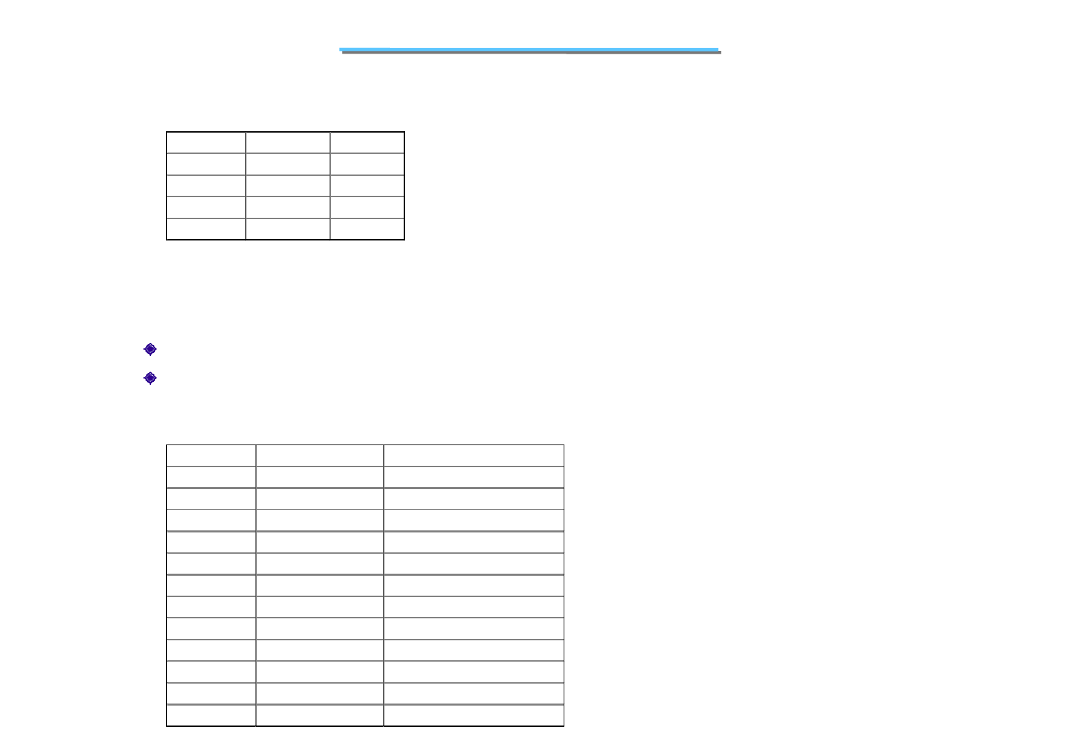
APPENDIX A WILLAMETTE CPU CORE FEQUENCY SELECTION
Bus Ratio Core Freq LINT[1]#NMI A20M# IGNNE# LINT[0]#/INTR
1/8 800MHz H H H H
1/10 1.00GHz H H L H
1/11 1.10GHz H H L L
1/12 1.2GHz H L H H
1/13 1.3GHz H L H L
1/14 1.4GHz H L L H
1/15 1.5GHz H L L L
1/16 1.6GHz L H H H
1/17 1.7GHz L H H L
1/18 1.8GHz L H L H
1/19 1.9GHz L H L L
1/20 2.0GHz L L H H
1/21 2.1GHz L L H L
1/22 2.2GHz L L L H
1/23 2.3GHz H H H L
1/24 2.4GHz L L L L
33
8170 N/B MAINTENANCE
APPENDIX B VOLTAGE INDENTIFICATION DEFFINITION
VID4 VID3 VID2 VID1 VID0 Vcc_max
111 1 1
VRM output off
11 1 1 0 1.100
11 1 0 1 1.125
11 1 0 0 1.150
11 0 1 1 1.175
11 0 1 0 1.200
11 0 0 1 1.225
11 0 0 0 1.250
10 1 1 1 1.275
10 1 1 0 1.300
10 1 0 1 1.325
10 1 0 0 1.350
10 0 1 1 1.375
10 0 1 0 1.400
10 0 0 1 1.425
10 0 0 0 1.450
0 1 1 1 1 1.475
0 1 1 1 0 1.500
0 1 1 0 1 1.525
0 1 1 0 0 1.550
0 1 0 1 1 1.575
0 1 0 1 0 1.600
0 1 0 0 1 1.625
0 1 0 0 0 1.650
0 0 1 1 1 1.675
0 0 1 1 0 1.700
0 0 1 0 1 1.725
0 0 1 0 0 1.750
0 0 0 1 1 1.775
0 0 0 1 0 1.800
0 0 0 0 1 1.825
0 0 0 0 0 1.850
34
8170 N/B MAINTENANCE
LCD CABLE REQUIREMENT
Each differential pair need meet maximum in impedance 100Ω
DC impedance have to meet maximum impedance 5m Ωin each line
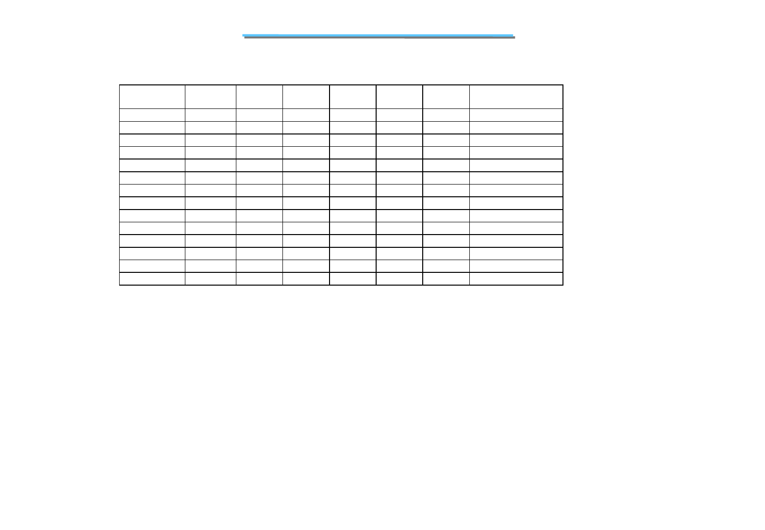
Unipac UB 141X01/Hyundai HT14X13/HannStar HSD141PX11 LCD Cable Pin Define
APPENDIX C FREQUENCY TABLE FOR BCLK[1:0]
BSEL1 BSEL0 Function
L L 100MHZ
LHRSV
HLRSV
HHRSV
Signal name M/B Pin Number LCD module pin number
LCDVCC 11
LCDVCC 22
GND 33
GND 44
GND 57
GND 610
TX2CLK+ 7NC
TXCLK+ 815
TX2CLK- 9NC
TRCLK- 10 14
GND 11 13
GND 12 16
35
8170 N/B MAINTENANCE
TX2OUT0+ 13 NC
TX2OUT1+ 14 NC
TX2OUT0- 15 NC
TX2OUT1- 16 NC
GND 17 NC
GND 18 NC
TX2OUT2+ 19 NC
TXOUT0+ 20 6
TX2OUT2- 21 NC
TXOUT0- 22 5
GND 23 19
GND 24 20
TXOUT2+ 25 12
TXOUT1+ 26 9
TXOUT2- 27 11
TXOUT1- 28 8
GND 29 NC
GND 30 NC
LCD_ID0 31 NC
+3VS 32 NC
LCD_ID1 33 NC
+3VS 34 NC
LCD_ID2 35 NC
+3VS 36 NC
NC 37 NC
NC 38 NC
NC 39 NC
NC 40 NC
36
8170 N/B MAINTENANCE
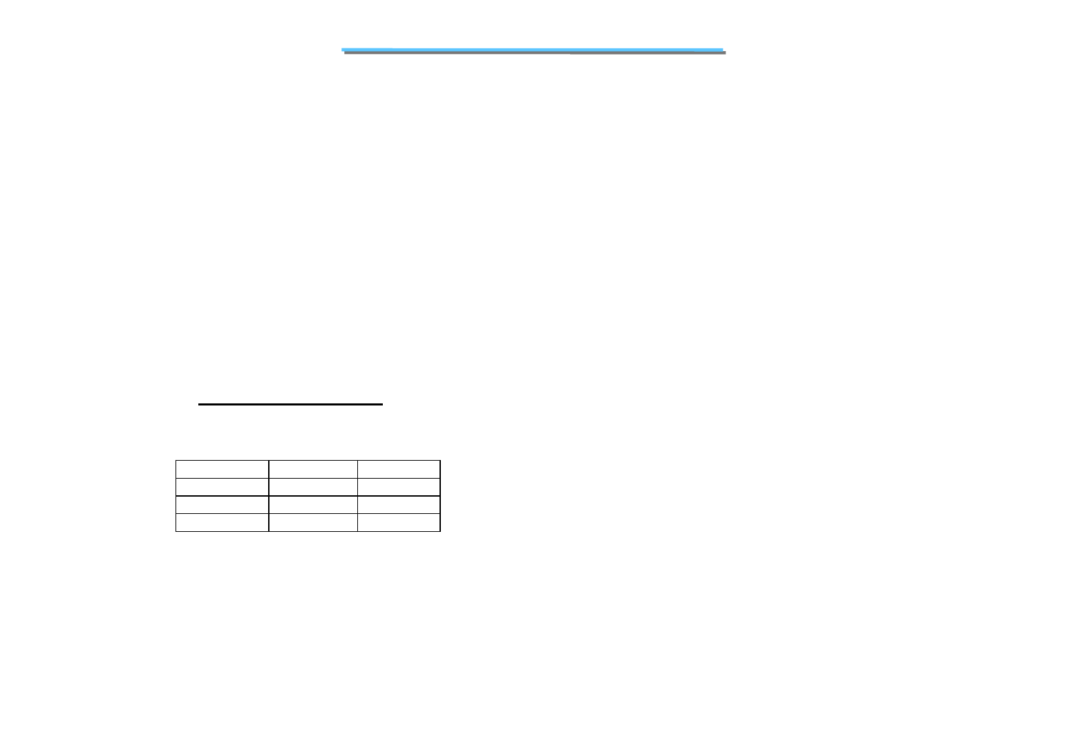
COM N141P1 LCD Cable Pin Define
LCD Panel Type Link Pin
Unipac 14.1" TFT:UB 141X01 31&32 tied together
Hyundai 14.1" TFT: HT14X13 33&34 tied together
HannStar 14.1" TFT: HSD141PX11 31&32,33&34 tied together
Signal name M/B pin Number LCD module pin number
LCDVCC 11
LCDVCC 22
GND 33
GND 44
GND 5NC
GND 6NC
TX2CLK+ 720
TXCLK+ 812
TX2CLK- 919
TXCLK- 10 11
GND 11 NC
GND 12 NC
TX2OUT0+ 13 14
TX2OUT1+ 14 16
TX2OUT0- 15 13
TX2OUT1- 16 15
GND 17 NC
GND 18 NC
TX2OUT2+ 19 18
37
8170 N/B MAINTENANCE
TXOUT+ 20 6
TX2OUT2- 21 17
TXOUT0- 22 5
GND 23 NC
GND 24 NC
TXOUT2+ 25 10
TXOUT1+ 26 8
TXOUT2- 27 9
TXOUT1-
28
7
GND
29
NC
GND
30
NC
LCD_ID0
31
NC
+3VS
32
NC
LCD_ID1
33
NC
+3VS
34
NC
LCD_ID2
35
NC
+3VS
36
NC
NC
37
NC
NC
38
NC
NC
39
NC
NC
40
NC
38
8170 N/B MAINTENANCE
LCD Panel ID Define Table
DISPLAY Link Pin
COM 14.1" SXGA+N141P1 35&36 tied together
LCD Panel LCD_ID2 LCD_ID1 LCD_ID0
Uniqac 001
Hyundai 010
HannStar 011
CMO 100

39
8170 N/B MAINTENANCE
1.5 BIOS Specification
1.5.1 BIOS Feature
@Inside BIOS for Intel 845 + ICH2 chipset
@ 256KB flash ROM
@ ACPI 1.0b Compliant (S1, S3, S4, S4BIOS)
@ Support APM 1.2 (POS, STR, STD)
@ SMBIOS 2.3.1
@ Support external 1.44MB USB Floppy
@ Support DVD-ROM and CD-ROM
@ Support Multi-boot function
@ Plug & Play for Devices
@ Support FIR
@ Silence Boot with Logo customized
@ Wake-up from USB
@ Fast boot bypass RAM/Floppy/CDROM testing
@ BIOS Lock function
Add the BIOS lock string at shadow memory address F000:E0C2

40
8170 N/B MAINTENANCE
@ Intel Pentium 4 Processors Willamette//Northwood, Support upto 1.7GHz, 400 Mhz FSB
@ Pentium 4 with 256K L2 Cache
@ 64Kbyte on-chip L1 Cache
@ CPU’s Power transition (Please refer to the chapter of Power Management for state definitions)
When in G0/Full-On, CPU can be in C0/C1/C2.
When in G1(STR)/G2(STD)/G3(Mechanical Off) State, CPU power is removed.
1.5.2.1 CPU
1.5.2.2 Memory System
@ Two SODIMM for SDRAM extension from 64MB to 512MB Pentium 4 with 256K L2 Cache
@ 400MHz Host Bus, 33MHz PCI Bus, 133MHz Memory Clock
@ Dynamically row power-down
@ Support Auto-refresh and Self-refresh command
@ Auto-detect CAS latency Programming
@ Memory Auto-sizing
@ 1/2/4 Bank SDRAM support, up to 4 page could open at any time
Please refer to the chapter of Power Management for state definitions. For PCI and PnP terms, please refer to
respective specifications
1.5.2 Component&Drives

41
8170 N/B MAINTENANCE
@VGA
---LCD panel could be turn on/off via function hotkey, or Lid switch if users define “Blank LCD” on cover
closed in SCU.
---When in G0/Full-On/Idle, VGA stays in D0 state, Panel stays on. However, if no VGA activities detected
for a specific period defined in SCU, VGA will go to D1 state, and Panel will be turned off.
---When in G2/G3/STD/Soft-Off/Mechanical Off State, VGA and Panel are power off.
---When in G1/Standby, VGA stays in D2 state, Panel stays off, Hsync/Vsync is cut.
---When in G1/STR, VGA stays in D3 state, Panel stays off, Hsync/Vsync is cut, especially, Note: VRAM
is shared on system DRAM, so no special circuit is provided for VRAM refresh when G1/STR.
@AUDIO
---When in G0/Full-On/Idle, Audio stays in D0 state
---When in G2/G3/STD/Soft-Off/Mechanical Off State, Audio is power off.
@MODEM
---Ring wake-up supported in G1/Standby/Suspend states.
---When in G0/Full-On/Idle, Modem stays in D0 state
---When in G2/G3/STD/Soft-Off/Mechanical Off State, Modem is power off.
@PMCIA(TI4410)
---PME# supported
@USB
---4 USB port are built in SB chipset (only 2 are supported in this model)
---Wake up from USB device is supported on POS/STR
1.5.2.3 PCI Devices
42
8170 N/B MAINTENANCE
---Ring wake-up supported in G1/Standby/Suspend states.
---When in G0/Full-On/Idle, PCMCIA stays in D0 state if PC card is inserted, and stays in D2 state once PC
card is removed.
---When in G2/G3/STD/Soft-Off/Mechanical Off State, PCMCIA is power off.
---When in G1/Standby, PCMCIA stays in D1 state.
---When in G1/Suspend, PCMCIA stays in D3 state.
@IEE1394(TI4410)
--- PME# supported
@LAN(RTL8139CL)
---PME# supported
---Ring wake-up supported in G1/Standby/Suspend states.
PCI Devices IDSEL
PCI Device IDESL Register Setting Bus/ Device/ Function
Intel 845 00 / 00 / 00
P2P (NB) 00 / 01 / 00
P2P (SB) AD14 00 / 30 / 00
LPC Bridge AD15 00 / 31 / 00
IDE AD15 00 / 31 / 01
USB #1 AD15 00 / 31 / 02
SMB AD15 00 / 31 / 03
USB #2 AD15 00 / 31 / 04
AC’97 AD15 00 / 31 / 05
MC’97 AD15 00 / 31 / 06
VGA 01 / 00 / 00
LAN AD18 02 / 02 / 00
PCMCIA AD19 02/ 03 / 00
IEEE 1394 AD19 02/ 03 / 01
43
8170 N/B MAINTENANCE
PCI IRQ Routing
CI Device PIRQ A PIRQ B PIRQ C PIRQ D PIRQ H PFA Bus/ Device/
Function
Intel 845 0x0000 00 / 00 / 00
P2P (NB) 0x0008 00 / 01 / 00
P2P (SB) 0x00F0 00 / 30 / 00
LPC Bridge 0x00F8 00 / 31 / 00
IDE 0x00F9 00 / 31 / 01
USB #1 INT D# 0x00FA 00 / 31 / 02
SMB 0x00FB 00 / 31 / 03
USB #2 INT C# 0x00FC 00 / 31 / 04
AC’97 INT B# 0x00FD 00 / 31 / 05
MC’97 INT B# 0x00FE 00 / 31 / 06
VGA INT A# 0x0100 01 / 00 / 00
LAN INT A# 0x0210 02 / 02 / 00
PCMCIA INT A# 0x0218 02/ 03 / 00
IEEE 1394 INT B# 0x0219 02/ 03 / 01
1.5.2.4 PCI Device
@Plug & Play Interface
---Plug and Play BIOS Spec. Rev. 1.0A Compliant
---No ESCD supported
@RTC
---User could setup current date and time in SCU. RTC must be Y2K compliant
---User could also setup a RTC wake-up event at any time of a month.

44
8170 N/B MAINTENANCE
@DMA
---ECP/FIR also use DMA but they are programmable
@PIC
---IRQ0 is used by the system timer
---IRQ1 is used by KBC (Key Board Controller)
---IRQ2 is used by slave PIC
---IRQ3 is used by IR
---IRQ5 is used by Audio
---IRQ7 is used by LPT port
---IRQ8 is used by RTC (Real Time Clock)
---IRQ9 is shared by SCI
---IRQ10 is used by LAN
---IRQ10 is used by PCMCIA
---IRQ10 is used by IEEE 1394
---IRQ10 is also shared by VGA
---IRQ12 is used by mouse
---IRQ13 is used internally by CPU to recognize FPU interrupts
---IRQ14 is used by IDE channel 1
---IRQ15 is used by IDE channel 2
---Preserve two IRQs (4, 6, 11) for other devices to use.

45
8170 N/B MAINTENANCE
@Super I/O
---SIO chip could enter a full power down mode once system enter Suspend states
---Printer Port
Print port will enter power down mode when G1/G2/G3/STD/Suspend/Standby state.
---IR Port
IR port will enter power down mode and IR module’s power will be cut off when G1/G2/G3/STD/
Suspend/Standby state.
@KBC
---H8 will automatically control its power state. Please refer to KBC’s specification
1.5.2.5 IDE Devices
@Hard Disk
---HD will enter standby mode whenever no access request is made.
---HD will enter standby mode when the system entering Standby state.
---HD will enter sleep mode when the system entering Suspend state.
@CDROM
---CD drive will enter standby mode whenever no access request is made.
---CD drive enter standby mode when the system entering Standby state.
---CD drive enter sleep mode when the system entering Suspend state
46
8170 N/B MAINTENANCE
1.5.2.6 AC’97 Device
@AC’97 Interface
@Audio Codec
---Enter the most power saving state during Suspend.
@Modem Codec
---Enter the most power saving state during Suspend
1.5.2.7 SMB
(1) South Bridge SMB BUS
@ SMBUS Device
SMB Device Read Addr Write Addr
SDRAM 0 0xA1 0xA0
SDRAM 1 0xA1 0xA0
CLK_GEN 0xD3 0xD2
@SDRAM
---Use SMB link to read configuration data from SDRAM
---Turn off clock if no SO-DIMM insert automatically when POST
@Clock Generator
---Spread spectrum is enabled during POST

47
8170 N/B MAINTENANCE
@ Thermal Sensor
---Sensed by H8
@ Charger
---Directly controlled by H8, please refer to KBC specification
1.5.2.8 Mechanics
@Button
---1 Power Button, 5 Easy Start Buttons, 1 E-Mail Received Button.
@LID Switch
---See 1.6.7
@LEDs
---All LEDs are controller via H8, Please refer to H8 Specification
@ FAN
---Controlled by H8
(2) H8 SMB BUS
@Battery Pack
---This is polling by KBC (H8)

48
8170 N/B MAINTENANCE
1.5.3.1 Introduction
1.5.3 BIOS Setup
SCU allows you to configure the BIOS settings. Those settings are vital for your notebook to identify the
types of installed devices as well as to utilize special features. Typical menu items include Date and Time,
the types of disk drives, and IDE settings. Special features include Power Saving and Password settings
The settings information is stored in the CMOS (Complementary Metal Oxide Semiconductor) RAM,
which is powered by a RTC backup battery.
You may need to run SCU when
1.5.3.2 Starting SCU
SCU is built into the system board. To run SCU, press [F2] during system startup. The main SCU screen
appears as shown in Figure 1.15.
* You see an error message on the screen requesting you to run SCU
* You want to restore the factory default settings
* You want to modify some specific settings

49
8170 N/B MAINTENANCE
Figure 1.16 Main SCU Screen
@ On the top line of the screen is the menu bar, which lists the titles of the available menus Each menu title
contains a pull-down menu, which displays items for settings
@ The middle section of the screen displays current settings of the system. If you open a pull-down menu
and select an item that provides multiple options, a submenu will pop up and let you make further
selections.
Insyde Software SCU Aug 23, 2001 2:34:12 pm
Startup Memory Disks Components Power Exit
Primary Master = 0 MB
Primary Slave = 0 MB
Secondary Master= 0 MB
Secondary Slave=0MB
Serial Port 2 = COM2, 2F8, IRQ3
Parallel Port = LPT1, 378, IRQ 7
Devices
Base = 640 KB
Extended = 64512 KB
Shadow = 176 KB
Reserved = 208 KB
Total RAM = 65536 KB
Cache (Ext) = 256 KB
Memory
CPU = Pentium 4
CPU Speed=0MHz
System
Press <Alt> Key to activate menus, and cursor keys to navigate. Mouse left
button, spacebar, and <Enter> keys accept menu item. Mouse right button and
<Esc> key cancel current action.
The SCU screen can be divided into three areas:

50
8170 N/B MAINTENANCE
@ The bottom window provides alternative information. Normally it gives the keyboard/mouse instructions
for moving around and making selections. When a menu item is highlighted, the window will provide
more detailed description of the item.
1.5.3.3 Moving Around and Making Selections
@ Using the Touch pad/Mouse
You are advised to use the touch pad or mouse. It is more straightforward than using the keyboard.
For most items, simply move the pointer with the touch pad/mouse and left-click on the intended item.
To cancel your selection, click the right button. For some items, you will need to select with the arrow
keys.
@ Using the keyboard
Keyboard information can be found at the bottom of the screen. You can also use the shortcut key, which
is highlighted in a different color on the screen.
Described below is the general procedure to complete a setting by use of the keyboard:
® Select a menu title with the left/right arrow key and press [Enter] to pull down the menu. You can
directly pull down a menu You can directly pull down a menu by pressing [Alt] and the shortcut key.
® From the pull-down menu, select an item with the up/down arrow key and press [Enter] to access the
submenu or change the setting, The submenu displays further options that you can select.
You must go through two or three levels to complete the setting for an item. In most cases, there are three
levels: menu title, pull-down menu, and submenu.
To move around and make selections, you can use both the touch pad/mouse and keyboard

51
8170 N/B MAINTENANCE
® For most menu items, pressing the [Tab] key will jump from one item to another, thus allowing you to
go through the items quickly. To confirm the changes you make, press [Enter] or select the OK button.
To cancel the changes, press [Esc] or select the Cancel button.
1.5.3.4 Startup Menu
The Startup pull-down menu, as shown below, contains some basic configuration and password settings of
the system
Date and Time >
Splash Boot Logo
√Fast Boot
Boot Device >
Set Admin password >
Set User password >
SCU Color Scheme >
Startup
@ Data and time
The “Date and Time” item sets the system date and time. When this item is selected, the submenu will
display as shown below:
Day 23 Hour 16
Month 8 Minute 56
Year 2001 Second 53
Date and Time
OK
OK Cancel
Cancel

52
8170 N/B MAINTENANCE
@ Splash Boot Logo
The “Splach boot Logo” item to enable or disable the big boot logo on screen when system is booting.
When this item is selected, no submenu will display. A check mark (√) indicates Enabled; an underline
(_) indicates Disabled. The default setting is Disabled
@ Fast Boot
The “Fast Boot” item, when enabled, speeds up the booting procedure by bypassing the memory test.
When this item is selected, no submenu will display. A check mark (√) indicates Enabled; an underline
(_) indicates Disabled. The default setting is Enabled.
@ Boot Device
The “Boot Device” item sets the sequence of booting device. When this item is selected, the submenu
will display as shown below.
( ) Hard Disk C
( ) CD-ROM Drive
(.) Diskette A
1st Boot Device
(.) Hard Disk C
( ) CD-ROM Drive
( ) Diskette A
( ) Hard Disk C
(.) CD-ROM Drive
( ) Diskette A
2nd Boot Device 3rd Boot Device
OK
OK Cancel
Cancel
Boot Device
The default setting is Diskette A, Hard Disk C, then CD-ROM Drive
NOTE: If you set all booting options to the same device (say, Hard Disk C),. then the notebook will try to
boot from that device only

53
8170 N/B MAINTENANCE
@ Set Admin Password
This item lets you set up administrator-level password. When this item is selected, the submenu will
display as shown below:
You can directly enter the new password if no password has previously existed. If a password has been
previously set up, you have to enter the correct old password before setting up a new one. In either case,
you have to enter the new password twice to complete the setting.
NOTE:
1. If you want to clear a previous password, you can enter the old password and leave the following fields
blank
2. The administrator password is required for booting and entering SCU, so the “Verify password when
…” setting can not be changed
Enter old ADMIN Password: ..........
Enter new ADMIN Password: ..........
Verify new ADMIN Password: ..........
[X] Boot System
[ ] Enter SCU
Verify password when...
OK
OK Cancel
Cancel
Set Admin password

54
8170 N/B MAINTENANCE
@ Set User Password
This item lets you set up user-level password. When this item is selected, the submenu will display as
shown below:
The procedure to set up the user password is the same as “Set Admin Password”.
NOTE:
1. You can not set up the user password unless the administrator password has been set up.
2. If both the administrator and user passwords are set up, only one password is required to boot the
system
3. To modify the SCU settings, you have to enter the administrator password. The user password only
allows you to browse the settings.
4. If the “Resume System” item is checked, the password is required only when the system is restored
from “Suspend-to-disk” status.
Enter old User Password: ..........
Enter new User Password: ..........
Verify new User Password: ..........
[X] Boot System
[ ] Enter SCU
Verify password when...
OK
OK Cancel
Cancel
Set User password

55
8170 N/B MAINTENANCE
@ SCU Color Scheme
The “Splach boot Logo” item select color set for your viewing. When this item is selected, the submenu
will display as shown below:
The default setting is “Color”.
(.) Color
( ) Alternate Color
( ) Black and White
( ) Reverse Black and
Select Color:
OK
OK Cancel
Cancel
SCU Color Scheme
1.5.3.5 Memory Menu
Cache Systems >
Memory
@ Cache System
( ) Disabled
(.) Write Back
L1 Cache
OK
OK Cancel
Cancel
Cache Systems
( ) Disabled
(.) Write Back
L2 Cache
The default settings of the “L1 Cache” and “L2 Cache” are “Write Back”.

56
8170 N/B MAINTENANCE
@ Internal HDC
The “Internal HDC” item sets if an internal hard drive is present.
When this item is selected, no submenu will display. A check mark (√) indicates Enabled; an underline
(_) indicates Disabled
The default setting is Enabled
1.5.3.6 Disk Menu
@ IDE Setting
The “IDE Settings” item sets the type of the hard disk drive in your system. When this item is selected,
the submenu will display as show below:
√Internal HDC
√IDE Setting >
Virus Alert >
Disks
( ) Standard
( ) Fast PIO
( ) Multiword DMA
( ) Ultra DMA-33
(.) ATA-66/100
HDD Timing
OK
OK Cancel
Cancel
IDE Settings
( ) Disabled
(.) Enabled
I/O 32 bit transfer
( ) Disabled
(.) Enabled
HDD Block transfer

57
8170 N/B MAINTENANCE
@ Virus Alert
The “Virus Alert” item, when enabled, gives warning messages if the hard disk boot sector (partition
table) has been changed
When this item is selected, no submenu will display. A check mark (√) indicates Enabled; an underline
(_) indicates disabled
The default setting is Disabled.
The “HDD Timing” item sets the data transmit mode of the hard drive. The default setting is Ultra DMA-33
The “I/O 32 bit transfer” item, if enabled, allows you to have better data transfer rate. This effect is more
noticeable under DOS system. The default setting is Enabled
The “HDD Block transfer” item, if enabled, allows you to use hard disk with large capacity. The default
setting is Enabled
1.5.3.7 Components
COM Ports >
LPT Port
√PS/2 Mouse Port
Legacy Usb >
√Keyboard Numlock
Keyboard Repeat >
Components
@ COM Ports
The “COM Ports” item sets the settings of COM Port A and B. When this item is selected, the submenu
will display as shown below:

58
8170 N/B MAINTENANCE
COM B is assigned to IR function. You can further select the IR mode in “Mode Setting for COM B”
item and DMA channel in“DMA Setting For Fast IR” when you select “Fast IR” in the mode setting.
@ LPT Ports
The “LPT Port” item sets the settings of LPT port. When this item is selected, the submenu will display
as shown below:
( ) Disabled
( ) COM1, 3F8, IRQ4
(.) COM2, 2F8, IRQ3
( ) COM3, 3E8, IRQ4
( ) COM4, 2E8, IRQ3
COM B I/O Settings
OK
OK Canel
Canel
COM Ports
( ) IrDA (HPSIR)
( ) ASK IR
(.) FAST IR
Mode Setting For COM B
(.) DMA 0
( ) DMA 1
( ) DMA 3
DMA Setting For Fast IR

59
8170 N/B MAINTENANCE
Your system supports EPP (Enhanced Parallel Port) and ECP (Extended Capabilities Port) standards
which turn the standard parallel port into a high speed bi-directional peripheral port. If you select ECP
item, you can further choose which DMA channel to use.
@ PS/2 Ports
The “PS/2 Mouse Port” item enables or disables the PS/2 mouse port
When this item is selected, no submenu will display. A check mark (√) indicates Enabled; an underline
(_) indicates Disabled. The default setting is enabled.
EPP Type : EPP 1.7
( ) None
(.) LPT1, 378, IRQ7
( ) LPT2, 278, IRQ5
( ) LPT3, 3BC, IRQ7
Port Address
OK
OK Cancel
Cancel
LPT Port
( ) Standard AT (Centronics)
( ) Bidirectional (PS-2)
( ) Enhanced Parallel (EPP)
(.) Extended Capabilities (ECP)
Port Definition
(.) DMA 0
( ) DMA 1
( ) DMA 3
DMA Setting For ECP Mode

60
8170 N/B MAINTENANCE
The “Enable USB Port” item enables or disables USB keyboard and USB mouse. The default setting is
enabled
The “Enable USB FDD” item enables or disables USB FDD. The default setting is enabled.
The “Enable USB FDD” item enables or disables boot from USB CDROM. The default setting is disabled
@ Keyboard Numlock
Keyboard Numlock” item sets if the numeric keypad will function
When this item is selected, no submenu will display. A check mark (√) indicates Enabled; an underline
(_) indicates Disabled. The default setting is Enabled.
@ Legacy USB
The “Legacy USB” item sets the settings of legacy USB port which enables or disables the USB keyboard,
USB mouse, USB floppy and USB CD-ROM in DOS and SCU. When this item is selected, the submenu
will display as shown below:
[X] Enable USB Port
[X] Enable USB FDD
[ ] Enable USB CDROM
OK
OK Cancel
Cancel
Legacy USB

61
8170 N/B MAINTENANCE
The “Key Repeat Rate” sets the repeat rate when you hold down a key, while the “Key Delay” item sets
the delaying time between key repeats
Note: If you disable this option, you can only activate the numeric keypad by holding down the [Fn] key
first, even when the Num Lock indicator is on. However, an externally-connected keyboard is not
affected by this feature.
@ Keyboard Repeat
The “Keyboard Repeat” item sets the repeat rate and delay time of key strokes. When this item is
selected, the submenu will display as shown below:
() 2cps
() 6cps
(.) 10 cps
()15cps
()20cps
()30cps
Key Repeat Rate
OK
OK Cancel
Cancel
Keyboard Repeat
( ) 1/4 sec
(.) 1/2 sec
( ) 3/4 sec
() 1sec
Key Delay

62
8170 N/B MAINTENANCE
@ Enable Power Saving
The “Enable Power Saving” item is the master control for the Power Management features. If this item
is disabled, all Power menu items except “Suspend Controls” will be automatically disabled.
When this item is selected, no submenu will display. A check mark (√) indicates Enabled; an underline
(_) indicates Disabled. The default setting is enabled
1.5.3.8 Power Menu
The Power pull-down menu, as shown below, contains the Power Management settings which help save
power
Power
√Enable Power Saving
Low Power Saving
Medium Power Saving
High Power Saving
√Customize >
Suspend Controls >
Resume Timer >
@ Low Power Saving / Medium Power Saving / High Power Saving / Customize
four items are mutually-exclusive options. You can select one of them. A check mark (√) indicates
Enabled; an underline (_) indicates is enabled an underline (_) indicates Disabled

63
8170 N/B MAINTENANCE
Descriptions of the four options are:
Options Descriptions
Max Performance Select this option for the pre-defined settings which allow maximum
Balanced Power Saving Select this option for the pre-defined settings which allow moderate
Max Power Saving Select this option for the pre-defined settings which allow longest
Customize Select this option for setting up your own preferences. When this
option is selected, the submenu will display as shown below that
allows you to set up Power Saving features. (See the next subsection
for information.)
Note: Under Windows98/Windows Me/Windows2000, have built-in ACPI configurations which will
override these settings When the “Customize” item is selected, the submenu will display as
shown below:
Video Timeout: Always On
Disk Timeout: Always On
Global Timeout: Always On
Monitor Video Activity: Disabled
OK
OK Cancel
Cancel
Customize
performance but shortest battery life.
performance and moderate battery life.
battery life but minimum performance.

64
8170 N/B MAINTENANCE
Video Timeout :
The “Video Timeout” item sets the time-out period for the monitor to power down if it is not in use
during the set period. The monitor will power up again when any key is pressed.
The available options are 30 Sec, 2 Min, 5 Min, 10 Min, 15 Min, 30 Min and Always On.
Disk Timeout:
The “Disk Timeout” item sets the time-out period for the hard disk to power down if it is not in use during
the set period. The hard disk will power up again when next accessed.
The available options are 30 Sec, 1 Min, 1.5 Min, 2 Min, and Always On.
Global Timeout:
The “Global Timeout” item sets the time-out period for initiating Standby mode. Whenever the system.
begins idling, the Power Saving starts the time-out for the Standby mode. If the system has been idled for
the specified time-out period, system will enter Standby mode.
If Standby mode is in effect, several system subsystems go into standby or off mode so that system power
will be reduced. The system will wake up from Standby mode when system activity is detected.
The available options are 1 Min, 2 Min, 4 Min, 6 Min, 8 Min, 12 Min, 16 Min, and Always On.
Monitor Video Activity
The “Monitor Video Activity” item sets if the video activity will be monitored. If enabled, any activity on
the screen (such as showing a movie title) will prevent the monitor from powering down.
The available options are Enabled and Disabled.

65
8170 N/B MAINTENANCE
@ Suspend Controls
The “Suspend Controls” item lets you micromanage several suspend features. When this item is selected,
the submenu will display as shown below:
Power Button Function: Power On/Off
Lid Switch Function: Blank LCD
Suspend Timeout: Never
Suspend-to-disk: Never
( ) Suspend To Disk
(.) Suspend To Ram
Suspend type
OK
OK Cancel
Cancel
Suspend Controls
Power Button Function :
This item sets the function of the power button. The available options are Power On/Off and Suspend/
Resume.
Note: When this item is set to “Suspend/Resume”, you can turn off the power by pressing the button for 4
seconds.
Lid Switch Function :
This item sets the sequential event when the top cover is closed while power is on. The available options
are Blank LCD, Suspend and CRT/TV Display.

66
8170 N/B MAINTENANCE
Suspend Type:
This item sets the suspend mode the system will enter. The available options are Suspend To Disk,
Suspend To RAM.
When Suspend-to-RAM mode is initiated, several subsystems will enter standby or power-off mode
to conserve power.The system will wake up from Suspend-to-RAM mode when a key is pressed. “
Resume Timer”, if enabled, can also wake up the system from Suspend-to-RAM mode.
When Suspend-to-Disk mode is initiated, the system preserves all the running application programs as a
file in a “suspend-to-disk partition” on the hard disk and then turns off automatically.
Suspend Timeout :
The “Suspend Timeout” item sets the time-out period for initiating suspend mode. This item works in
conjunction with previous "Global Timeout" item. When the system enters standby mode, the Power
Saving starts the time-out for the Suspend mode. If the system has been in standby mode for the specified
time-out period, system will enter Suspend mode.
The Suspend mode is determined by the “Suspend Type” item in the “Suspend Controls” submenu. It
can be Suspend-to-RAM, Suspend-to-Disk.
The available options are 1 Min, 5 Min, 10 Min, 20 Min, 20 Min, 30 Min, and Never.
Suspend-to-disk:
The “Suspend-to-disk” item sets the time-out period for initiating suspend-to-disk mode. This item works
in conjunction with previous "Suspend Timeout" item. When the system enters suspend-to-ram mode, the
Power Saving starts the time-out for the Suspend-to-disk mode. If the system has been in suspend-to-ram
mode for the specified time-out period, system will enter suspend-to-disk mode.
The available options are 1 Min, 5 Min, 10 Min, 20 Min, 30 Min, and Never.

67
8170 N/B MAINTENANCE
@ Resume Timer
The Resume Timer” item sets the date and time the system will resume from suspend mode. When this
item is selected, the submenu will display as shown below :
Alarm Resume : Disable
Resume Month 8
Resume Day 8
Resume Hour 12
Resume Minute 0
OK
OK Cancel
Cancel
Resume Timer
The default setting is Disabled
1.5.3.9 Exit Menu
The Exit pull-down menu, as shown below, displays ways of exiting SCU. After finished with your
settings, you must save and exit SCU so that the settings can take effect
Exit
Save and Exit >
Exit (No Save) >
Default Settings >
Restore Settings >
Version Info >

68
8170 N/B MAINTENANCE
Choices Descriptions
Save and Reboot Save changes and reboot the system.
Exit (No Save) Exit without saving the changes you have made.
Default Settings Load factory default values for all the items.
Restore Settings Restore previous values for all the items.
Version Info Show BIOS version information
1.5.4 Function Hotkeys
Fn + F5 Toggle display output. The display switch sequence, please refer to chapter 6
Fn + F6 Brightness Down (16 levels)
Fn + F7 Brightness Up (16 levels)
Fn + F10 Enable/Disable battery warning beep
Fn + F11 Panel on/off
Fn + F12 Suspend to RAM or disk
Descriptions of the Exit choices are:
69
8170 N/B MAINTENANCE
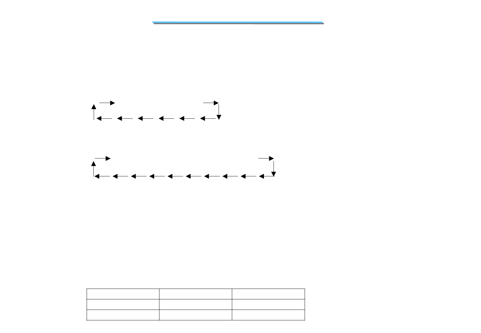
1.5.5 Display Out
When you boot the system with CRT, display output is LCD&CRT mode.
When boot with CRT, the display switch sequence by hotkey FnF5 is as following:
LCD&CRT->LCD->CRT
When boot with CRT and TV, the display switch sequence by hotkey FnF5 is as following:
LCD&CRT->TV&CRT->TV->LCD->CRT
1.5.6 LID
@ In Non-ACPI Operating System:
LID switch function is dependent on the setting in BIOS setup menu.
“Blank LCD” - LCD will be blank when LID is closed.
Before LID is closed LID is closed LID is opened
LCD is active LCD is blank LCD is active
LCD is blank LCD is blank LCD is blank
70
8170 N/B MAINTENANCE
“Suspend” -system will enter suspend mode when LID is closed.
@ In ACPI Operating System:
The LID switch function is dependent on the setting of the Power Management in the operating system.
Before LID is closed LID is closed LID is opened
System is On System enters Suspend System still in Suspend
System in Suspend System still in Suspend System still in Suspend
“CRT/TV Display” -display will be switched to CRT/TV when LID is closed.
When the LID is closed, the LCD will be inactive and external display device will be active.
When the LID is opened, the display devices status (active/inactive) will be restored to the
state before the LID is closed.
Some special conditions are list below.
Before LID is closed LID is closed LID is opened
LCD (active)
CRT (present, inactive)
TV(present, inactive)
LCD (inactive)
CRT (active)
TV(inactive)
LCD (active)
CRT (inactive)
TV(inactive)
LCD (inactive)
CRT/TV is present
LCD (inactive)
CRT/TV is plugged out
LCD (active)
CRT/TV is not present
71
8170 N/B MAINTENANCE
1.5.7 VGA Resolution of Windows 98/Me Driver
(Need Modifying via VGA Driver)
Resolution Color
640*480 256, 16bit, 32bit
800*600 256, 16bit, 32bit
1024*768 256, 16bit, 32bit
LCD(LCD&CRT)
CRT(TV)
Resolution Color
640*480 256, 16bit, 32bit
800*600 256, 16bit, 32bit
1024*768 256, 16bit, 32bit
1280*1024 256, 16bit
1600*1200 256, 16bit
Resolution Color
640*480 256, 16bit, 32bit
800*600 256, 16bit, 32bit
TV(TV+CRT)

72
8170 N/B MAINTENANCE
1.5.8 LED Indicators
System has nine status LED indicators to display system activity which include below LCD panel unit and
above keyboard:
1.5.8.1 Three LED indicators below LCD panel unit:
From left to right that indicate AC POWER, BATTERY POWER and BATTERY STATUS
®AC POWER: This LED lights green when the notebook is being powered by AC, and flash (on 1
second, off 1 second ) when Suspend to DRAM is active using AC power. The LED is off when the
notebook is off or powered by batteries, or when Suspend to Disk.
®BATTERY POWER:This LED lights green when the notebook is being powered by batteries, and
flashes (on 1 second, off 1 second ) when Suspend to DRAM is active using battery power. The LED
is off when the notebook is off or powered by AC, or when Suspend to Disk.
®BATTERY STATUS:During normal operation, this LED stays off as long as the battery is charged.
When the battery charge drops to 10% of capacity, the LED lights red, flashes per 1 second and beeps
per 2 second. When AC is connected, this indicator glows green if the battery pack is fully charged, or
orange (amber) if the battery is being charged.
1.5.8.2 Five LED indicators in front of palm rest:
From left to right that indicates CD-ROM/MO, HARD DISK DRIVE, , NUM LOCK, CAPS LOCK and
SCROLL LOCK.

73
8170 N/B MAINTENANCE
1.5.9 Power Management
1.5.9.2 Device power state
1.5.9.1 Features
® APM 1.2/1.1/1.0 compliant
® Battery warning beep
® Battery low suspend to RAM/disk
® Cover switch close to panel off, standby, or suspend
® Hot-key suspend
® Hot-key panel on/off
® Auto clock throttling to prevent overheating
® ACPI 1.0 compliant
® User programmable standby/suspend timers and sustained events when OS doesn’t support APM/ACPI
Note: Each device power states are described in the chapter titled Components & Drives. Please refer to
those paragraphs. BIOS will not automatically manage devices’ power states if ACPI engaged or APM
engaged but disabled.
1.5.8.3 Mail/Blue-Tooth LED indicators in front of palm rest:
The left side green LED flashing means new mail coming. Otherwise the LED is always OFF. The right
side red LED ON means Blue-Tooth module turn ON.

74
8170 N/B MAINTENANCE
Suspend States:
S1 – CPU stop, no system context lost
S2 – CPU stop, no system context lost except CPU & cache’s context is lost
S3 – CPU stop, the whole system context lost except system memory content is maintained
S4 – CPU stop, all system context saved to nonvolatile media before lost.
S5 – Soft Off
CPU States:
C0 – CPU is working
C1 – CPU is in Auto Halt Mode
C2 – CPU is in Quick Start Mode, the system will maintain the cache coherency
C3 – CPU is in Deep Sleep Mode, the system must disable any event which could make the cache
lost coherency. This model is not support C3 mode.
Definitions when ACPI engaged
Global States:
G0 – Global system is working
G1 – Global system is sleeping
G3 – Global system is mechanical-off
1.5.9.3 System power state

75
8170 N/B MAINTENANCE
Enter Condition:
Idle -Entered when CPU Idle Function is called
Standby -Entered when SetPowerState(Standby) Function is called
Suspend -Entered when SetPowerState(Suspend) is called, and user select STR in SCU
Save to Disk -Entered when SetPowerState(Suspend) is called, and user select STD in SCU
Resume Event :
Idle -Resume when CPU Busy Function is called
Standby -Resume only when keyboard device have activities, when ring come in on internal
modem or PCMCIA card. The reason for not selecting track-pad as resume event is that,
it’s too sensitive sometimes
Suspend -Entered when SetPowerState(Suspend) is called, and user select STR in SCU
Save to Disk -Entered when SetPowerState(Suspend) is called, and user select STD in SCU
System States:
Full On -Full running state, the system is in optimized performance
Idle -Clock throttling state, CPU is running between C0 & C2 states
Standby -Same as S1/S2 above
Suspend -Same as S3 above (Including save-to-ram and power-on-suspend)
Save to Disk -Same as S4 above
Note: When Save to Disk partition is not made on disk, BIOS will choose Save to RAM instead of Save to Disk
1.5.9.4 Definitions when APM engaged

76
8170 N/B MAINTENANCE
Exception -Note, when APM is disabled, BIOS should disable all timers and not to automatically
power manage devices. Furthermore, the APM BIOS will neither response to CPU Idle
Function, nor recognize the time periods set for Standby and Suspend in SCU.
System States:
Full On -Full running state, the system is in optimized performance
Idle -No Idle mode support in this situation .
Standby -Same as S1/S2 above
Suspend -Same as S3 above (Including save-to-ram and power-on-suspend)
1.5.9.5 Definitions when no APM or ACPI engaged
Standby -When all the devices have no system activities for a specific time period, BIOS will
inform a standby event once OS calls GetPMEvent Function.
Suspend -When all the devices have no system activities for a specific time period, BIOS will
inform a suspend event once OS calls GetPMEvent Function.
Activities -System activities is defined in SCU one by one. SCU also includes two columns for the
time periods for Standby and Suspend. In addition, Keyboard activity is always one of
the system activities. Whenever any system activities detected, timers for Standby and
Suspend are reloaded into the value specified. By the way, RTC could also
programmable to wake up the system from Standby and Suspend states.
Event Notifications:

77
8170 N/B MAINTENANCE
Special Events:
-Cover switch, or called lid could trigger an event to LCD panel off, Standby(S1/S2), or
Suspend(S3/S4). The exact state triggered is selected in SCU
-Power button is also a resume event for all power saving mode except the Idle state
-When battery capacity is low under 10% while AC is not plug-in, system will begin to
alert via PC speaker. User could also press Fn+F10 to disable/enable the warning beep.
Once the battery capacity is critically under 3%, system BIOS will try to force the whole
system into the STD state.
Resume Event:
Standby -Resume when keyboard/trackpad/PS2 devices have activities, when ring come in on
internal modem or PCMCIA card, or when COM has activities if user select to resume
from COM port
Suspend -Same as resume events for Standby state
Save to Disk -Resume when User push power button
Enter conditions:
-The timers for Standby and Suspend mode when APM engaged are also applied to this
situation that no APM or ACPI engaged.
Note: When Save to Disk partition isn’t made on disk, BIOS will choose Save to RAM instead of Save to Disk
Save to Disk -Same as S4 above

78
8170 N/B MAINTENANCE
1.5.9.7 ACPI
@Custom Software SMI Command for ACPI(Modifying if Need)
(1) 0x81 : Notify BIOS that the system is going to enter S3
(2) 0x82 : Notify BIOS that the system wake up from S3
(3) 0x83 : Get AC Status
(4) 0x84 : Get Battery General Status (_STA)
(5) 0x85 : Get Battery Information (_BIF)
(6) 0x86 : Get Battery Present Status (_BST)
(7) 0x87 : Get Battery Trip Point (_BTP)
1.5.9.6 Save to disk partition utility
0VMAKFIL.EXE S support partition only
Usage: 0VMAKEFILE.EXE -P<partition size>
< Partition size>= total of system RAM size + total of video RAM size
79
8170 N/B MAINTENANCE
Index Description Comment
0x40 AC Status Bit0: 0 – AC present
1 – AC not present
0x41 Battery Info 1 Bit0:
Bit1: 0 – NiMH
1 – LiON
0x42 Battery Info 2 Bit0: 0 – Battery not present
1 – Battery present
Bit1:
Bit2: 0 – no force charge
1 – force charge
Bit3:
0x43 Battery Info 3 Bit0: 0 – no trickle charge
1 – trickle charge
0x44~0x45 Last Full Charge Capacity
0x46~0x47 Remaining Capacity
0x48~0x49 Design Capacity
0x4A~0x4B Design Voltage
0x4C SOC1
0x4D Current Voltage
0x4E Battery Trip Point
@CMOS mapping for ACPI battery control method to use (Modifying if Need)
1.5.10 Post Massage
Reference to 7.2
80
8170 N/B MAINTENANCE
1.5.11 GPIO settings
1.5.11.1 South Bridge
@GPIO Signal
I/O Address GPIO Register I/O Address Map
GPIO # Multi. Func./Note Type Signal Name / Description Signal Select Register
0 REQ[A]# I
1 REQ[B]#/REQ[5]# I
2 Not Implement N/A
3 PIRQ[F]# I
4 PIRQ[G]# I
5 Not Implement N/A
6 I
7 I
8 I SCI#
9 Not Implement N/A
10 Not Implement N/A
11 SMBALERT# I
12 I EXTSMI#
13 I
14 Not Implement N/A
15 Not Implement N/A
16 GNT[A]# O
17 GNT[B]#/GNT[5]# O
18 O
19 O ENABKL_MSK#
20 O CDROM_PWRON#
21 O HDD_PWRON#
81
8170 N/B MAINTENANCE
22 O DRAMENA
23 O
24 I/O 1394WR# GPIOBASE+04 bit24 = 0
25 I/O PCIRST_MSK# GPIOBASE+04 bit25 = 0
26 Not Implement N/A
27 I/O GATE1394# GPIOBASE+04 bit27 = 0
28 I/O SPK_OFF GPIOBASE+04 bit28 = 0
29 Not Implement N/A
30 Not Implement N/A
31 Not Implement N/A
82
8170 N/B MAINTENANCE
2. System Assembly & Disassembly
2.1 System View
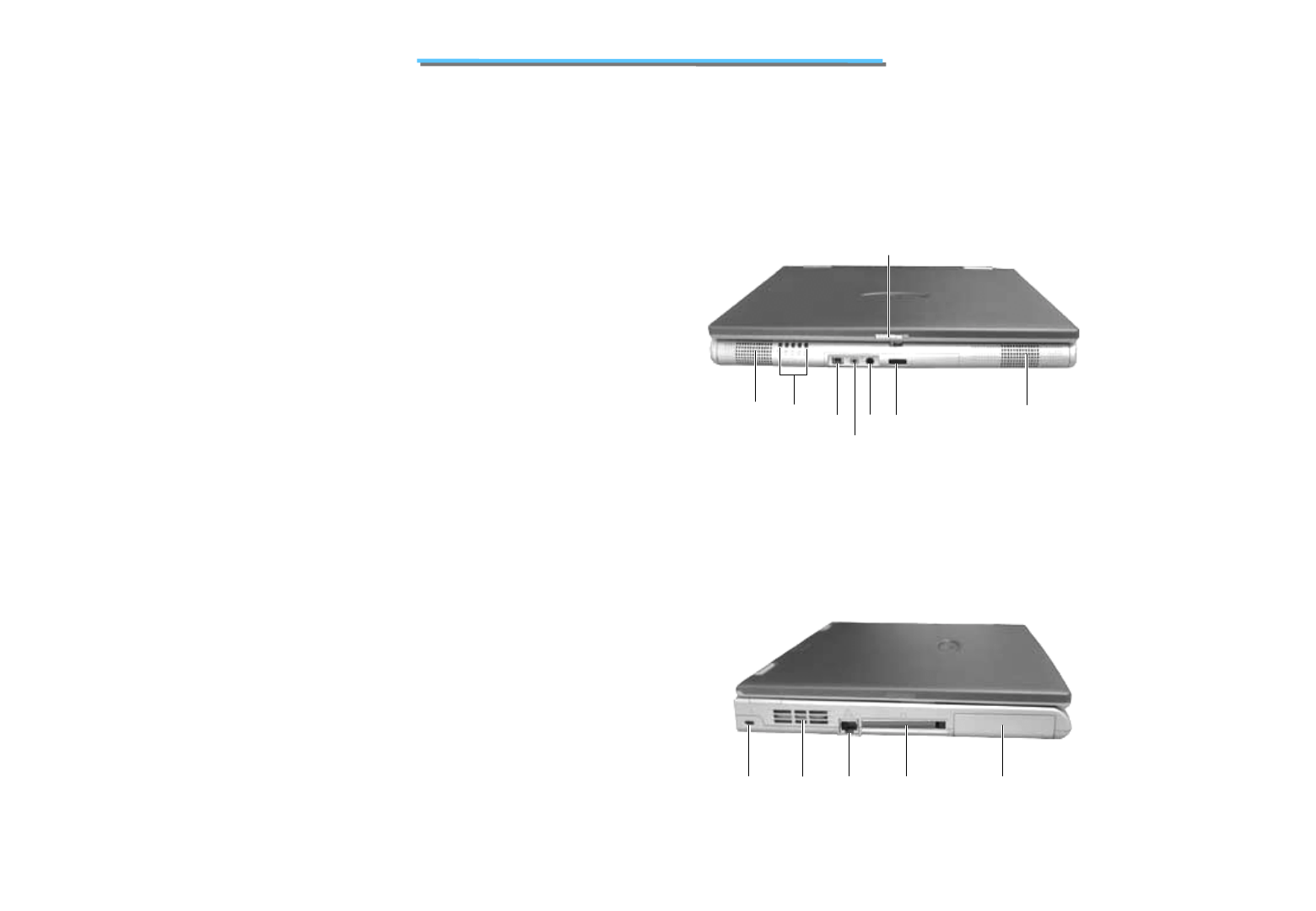
2.1.1 Front View
Stereo Speaker Set
Device Indicators
Mini IEEE1394 Connector
Audio Input Connector
Line Out Phone Jack
Volume Control
Top Cover Latch
2.1.2 Left-Side View
Kensington Lock
Ventilation Openings
RJ-45 Connector
PC Card Slot
Hard Disk Drive
83
8170 N/B MAINTENANCE
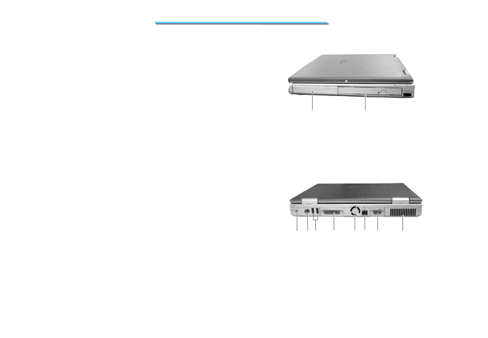
2.1.3 Right-Side View
Battery Pack
CD-ROM/DVD-ROM Drive
2.1.4 Rear View
Power Connector
S-Video Output Connector
USB Ports
Parallel Port
D/D Fan
RJ-11 Connector
VGA Port
Ventilation Openings
84
8170 N/B MAINTENANCE
2.1.5 Top-Open View
LCD Screen
Microphone
Keyboard
Touch pad
Power Button
Easy Start Buttons
Battery Charge Indicator
Battery Power Indicator
AC Power Indicator
85
8170 N/B MAINTENANCE
2.2 System Disassembly
The section discusses at length each major component for disassembly/reassembly and show corresponding
illustrations. Use the chart below to determine the disassembly sequence for removing components from the
notebook.
NOTE: Before you start to install/replace these modules, disconnect all peripheral devices and make sure the
notebook is not turned on or connected to AC power.
Modular Components
LCD Assembly Components
Base Unit Components
NOTEBOOK
2.2.1 Battery Pack
2.2.2 Keyboard
2.2.3 CPU
2.2.4 HDD Module
2.2.5 CD/DVD-ROM Drive
2.2.6 SO-DIMM
2.2.7 LCD Assembly
2.2.8 LCD Panel
2.2.9 Inverter Board
2.2.10 System Board
2.2.11 Touch pad
2.2.12 Modem Card
86
8170 N/B MAINTENANCE
2.2.1 Battery Pack
Disassembly
1. Carefully put the notebook upside down.
2. Slide the release lever to the “unlock” ( ) position (), then slide and hold the release lever outwards and
pull the battery pack out of the compartment (). (Figure 2-1)
Figure 2-1 Remove the battery pack
Reassembly
1. Push the battery pack into the compartment. The battery pack should be correctly connected when you hear a
clicking sound.
2. Slide the release lever to the “lock” ( ) position.
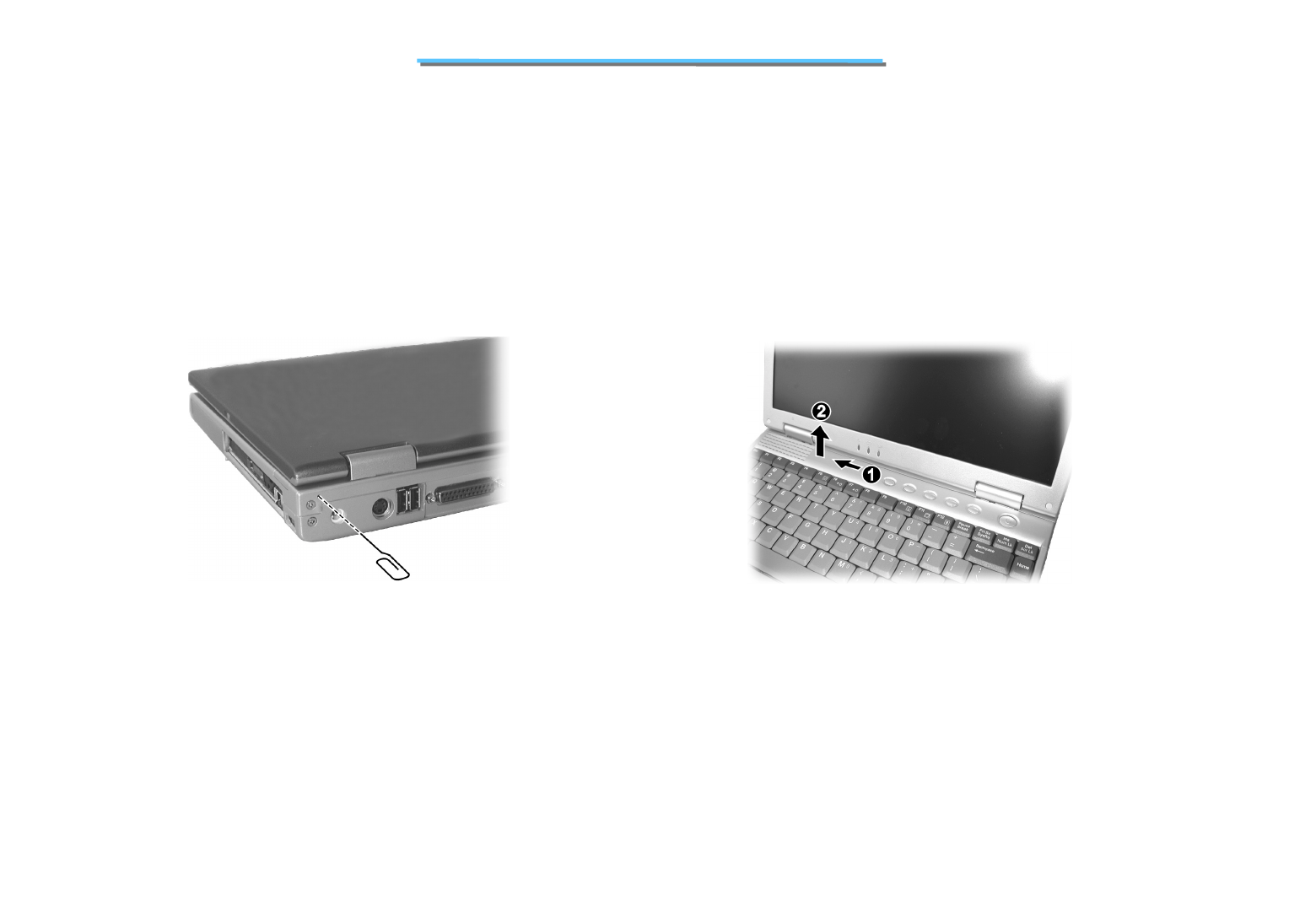
87
8170 N/B MAINTENANCE
2.2.2 Keyboard
Disassembly
1. Insert a small rod, such as a straightened paper clip, into the eject hole near the power
connector of the notebook. (Figure 2-2)
Figure 2-2 Insert a rod easy to remove Figure 2-3 Remove LED Panel
LED Panel
2. Open the top cover. Push the rod firmly and slide the LED panel to the left (). Then lift the LED panel up from
the left side () (Figure 2-3)
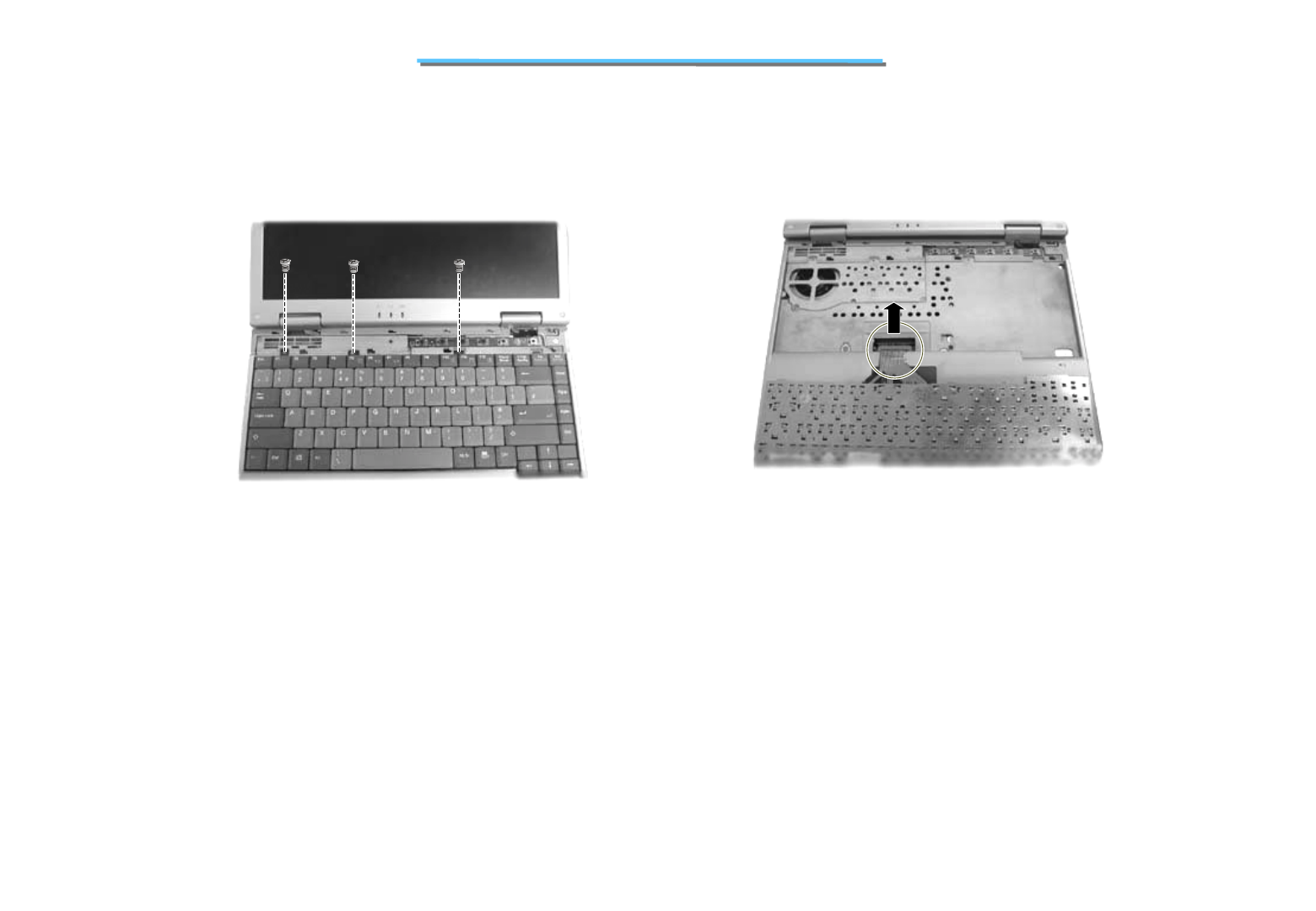
88
8170 N/B MAINTENANCE
Figure 2-4 Remove three Screws Figure 2-5 Remove keyboard
Reassembly
1. Reconnect the keyboard cable and fit the keyboard back into place.
2. Replace the LED panel.
3. Remove three screws fastening keyboard on the base unit cover. (Figure 2-4)
4. Slightly lift up the keyboard and disconnect the cable from the system board to detach the keyboard. (Figure 2-5)
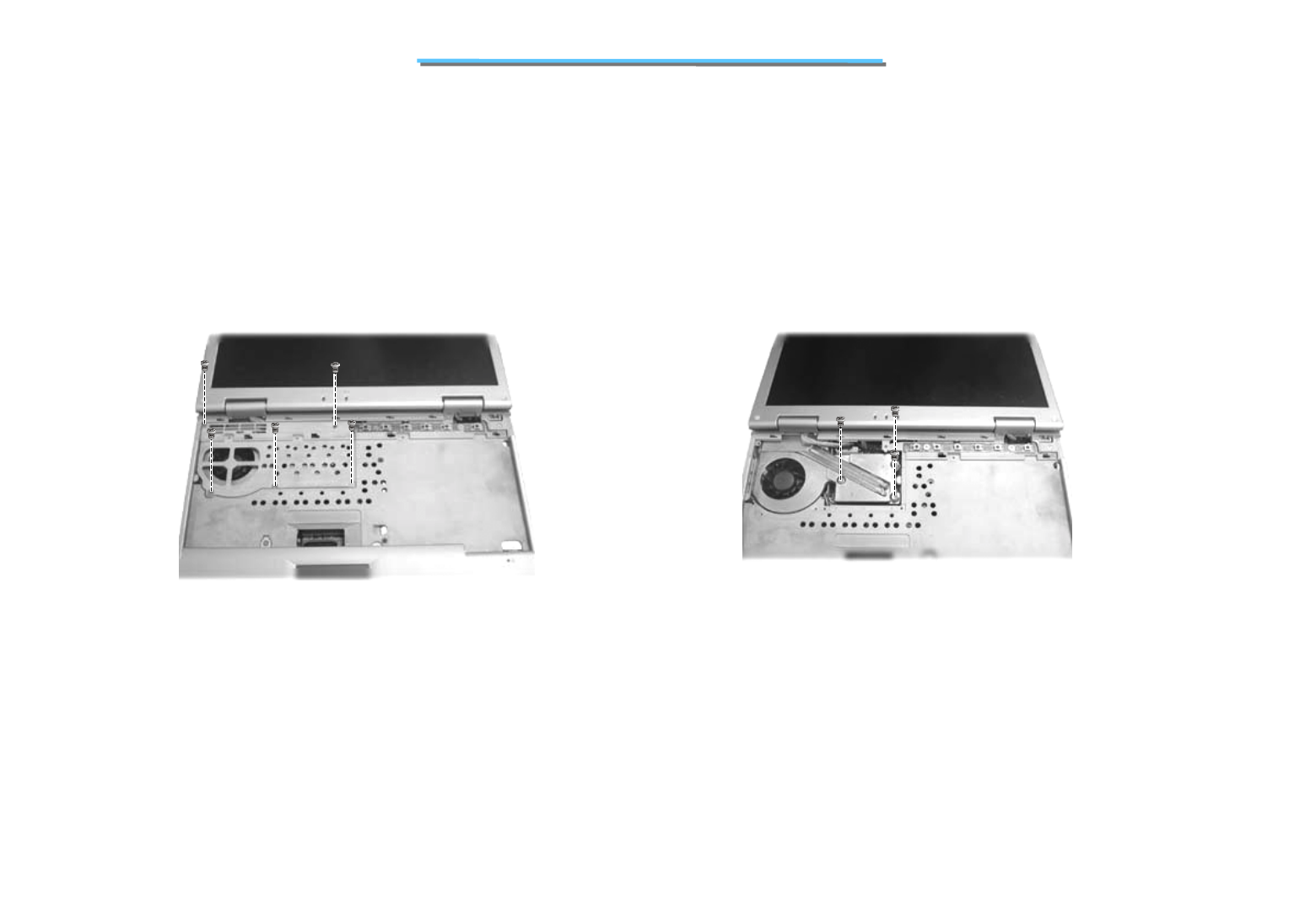
89
8170 N/B MAINTENANCE
2.2.3 CPU
Disassembly
1. Remove the LED panel and keyboard to access the CPU compartment. (See section 2.2.2 Disassembly.)
2. Remove five screws locking the heatsink cover. (Figure 2-6)
Figure 2-6 Remove the cover Figure 2-7 Remove the heatsink
3. Remove three screws locking the heatsink. (Figure 2-7)
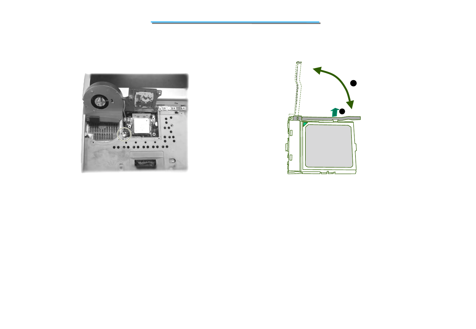
90
8170 N/B MAINTENANCE
5. push the lever to the right. Then lift up the lever to the vertical position. Finally, remove the existing CPU.
4. Disconnect the fan’s power cord from the system board, then lift up the heatsink. (Figure 2-8)
Figure 2-8 Remove the fan’s power cord Figure 2-9 Remove the CPU
Reassembly
1. Carefully, Align the arrowhead corner of the CPU with the beveled corner of the socket, then insert the CPU
pins into the holes. Place the lever back to the horizontal position and push the lever to the left .
2. Connect the fan’s power cord to the system board, fit the heatsink onto the top of the CPU and secure with
three screws.
3. Replace the keyboard .Then replace LED panel.
1
2
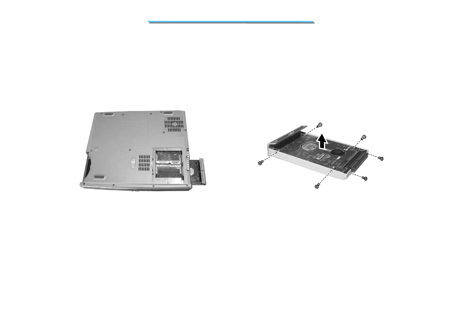
91
8170 N/B MAINTENANCE
2.2.4 HDD Module
Disassembly
1. Carefully put the notebook upside down.
2. Remove one screw and slide the HDD module out of the compartment. (Figure 2-10)
Figure 2-10 Remove HDD Module Figure 2-11 Disassemble the hard disk
3. Remove six screws to separate the hard disk drive from the metal shield. (Figure 2-11)
1. To install the hard disk drive, place it in the bracket and secure with six screws.
2. Slide the HDD module into the compartment and secure with one screw.
Reassembly
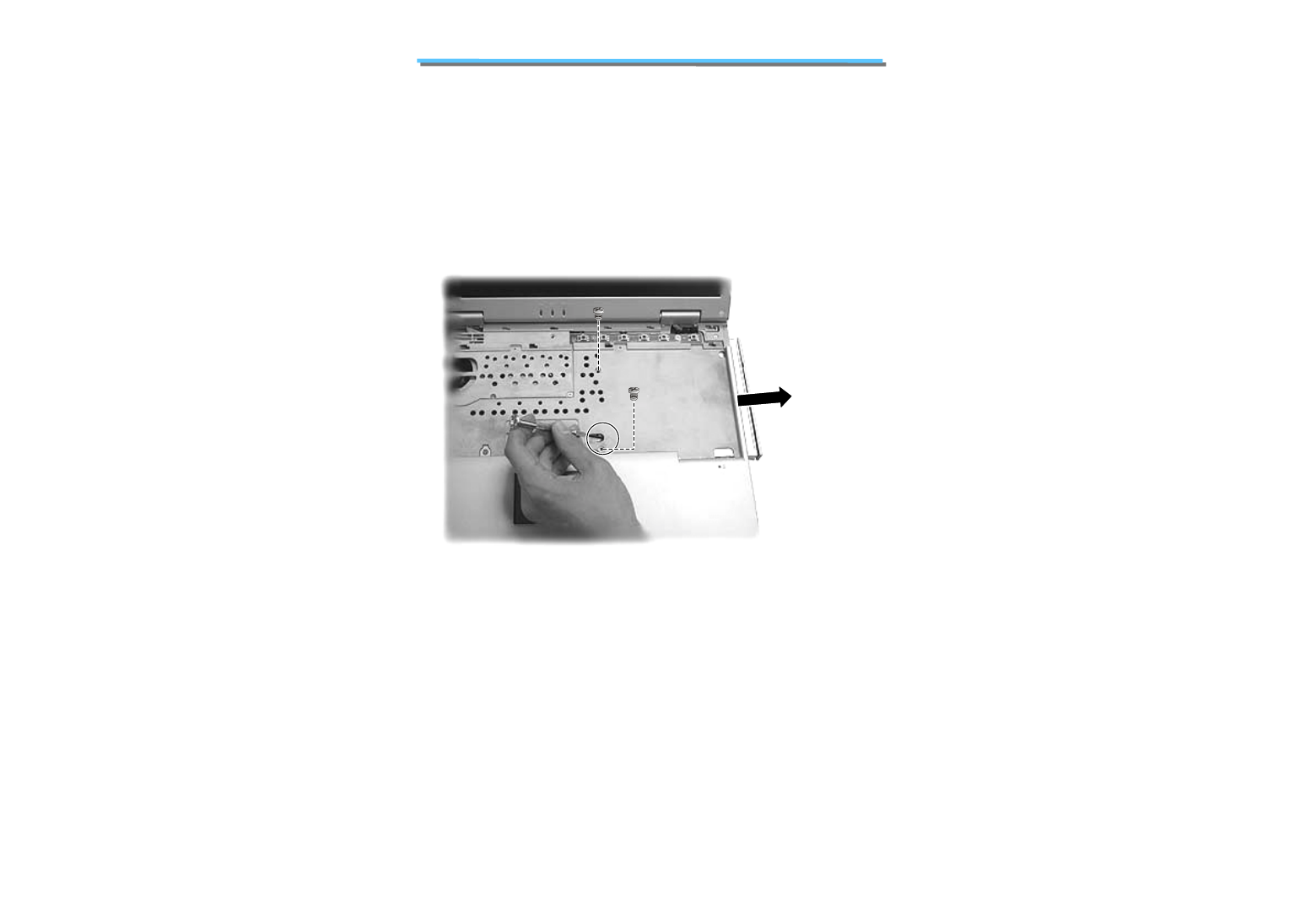
92
8170 N/B MAINTENANCE
Disassembly
1. Remove the LED panel and keyboard. (See section 2.2.2 Disassembly.)
2. Remove two screws locking the CD/DVD-ROM drive. (Figure 2-12)
Figure 2-12 Push out the CD/DVD -ROM drive
3. Use the screwdriver to push the metal pad to the right and the CD/DVD-ROM drive will pop out. Hold the
CD/DVD-ROM drive and slide it outwards carefully. (Figure 2-12)
1. Push the CD/DVD-ROM drive into the compartment.
2. Secure the CD/DVD-ROM drive with two screws.
3. Replace the keyboard and LED panel.
2.2.5 CD/DVD-ROM Drive
Reassembly
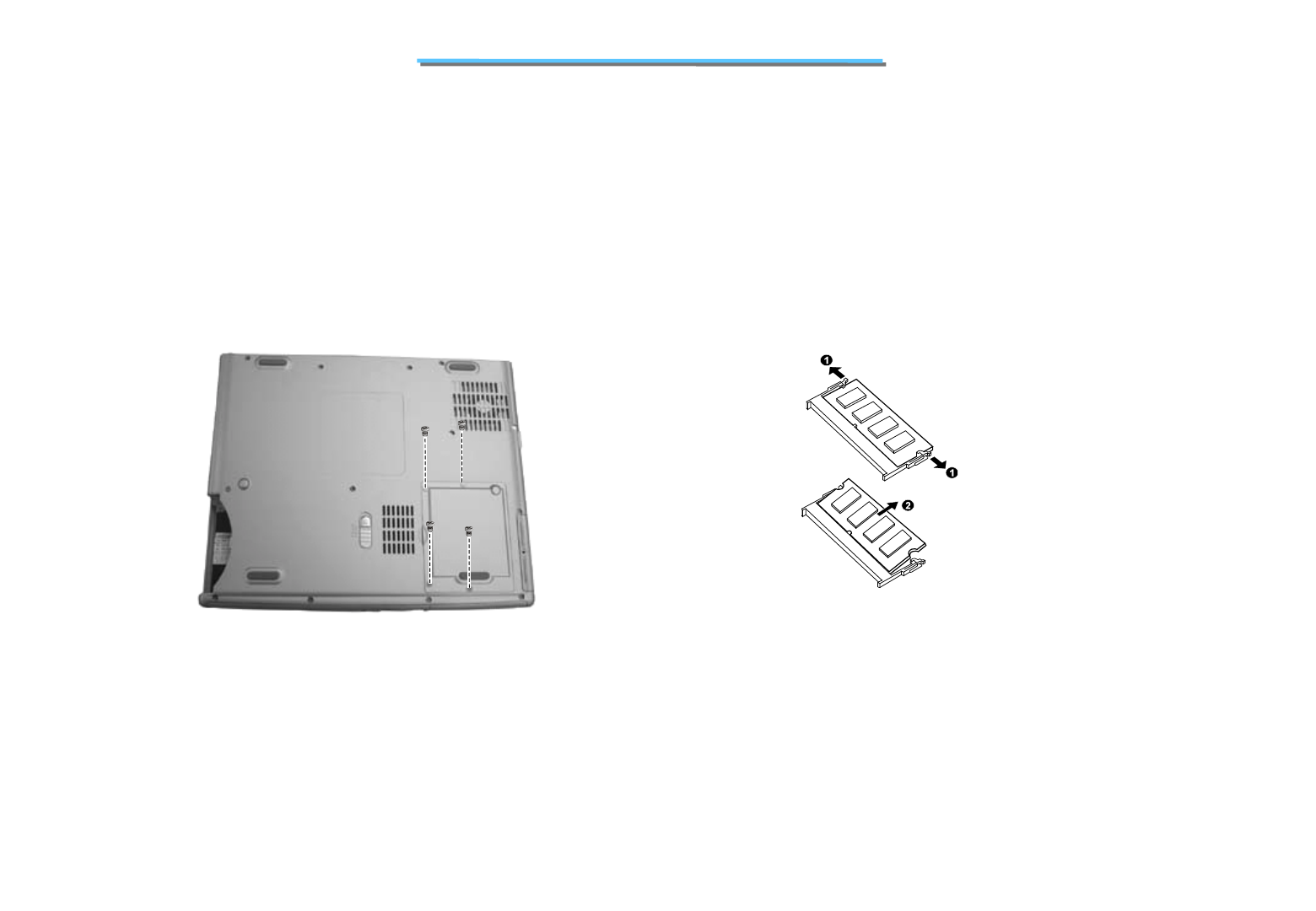
93
8170 N/B MAINTENANCE
Disassembly
1. Carefully put the notebook upside down.
2. Remove four screws to access the SO-DIMM socket.
3. Pull the retaining clips outwards () and remove the SO-DIMM (). (Figure 2-13,14)
Figure 2-13 Remove the SO-DIMM Cover Figure 2-14 Remove the SO-DIMM
Reassembly
1. To install the SO-DIMM, match the SO-DIMM's notched part with the socket's projected part
and firmly insert the SO-DIMM into the socket at 20-degree angle. Then push down until the
retaining clips lock the SO-DIMM into position.
2. Replace three screws to lock the SO-DIMM socket cover.
2.2.6 SO-DIMM
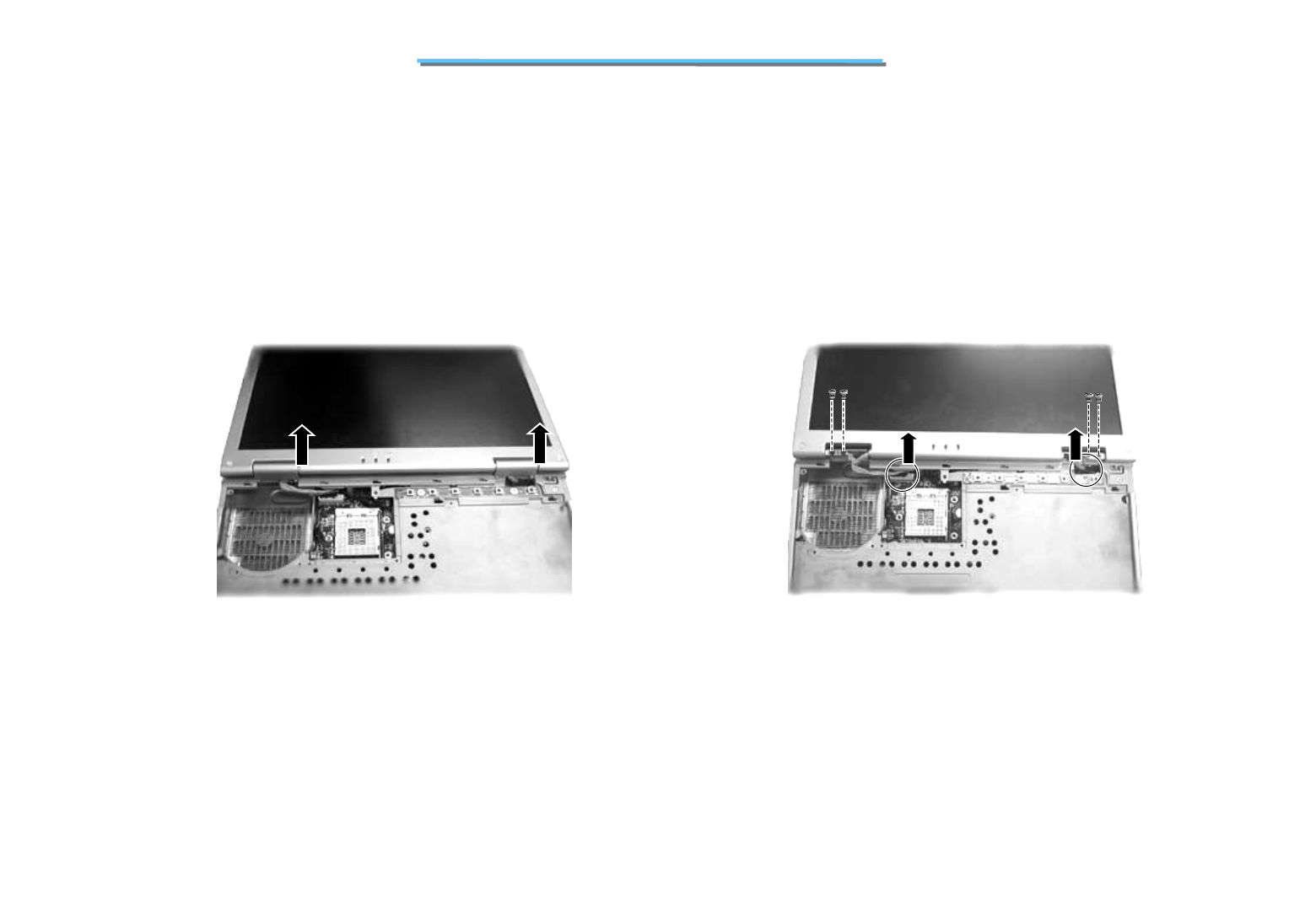
94
8170 N/B MAINTENANCE
Disassembly
1. Open the top cover. Remove the LED panel, keyboard, and heat sink . (See section 2.2.2 and 2.2.Disassembly.)
2. Pull out the antenna from the CPU compartment.
3. Remove the two hinge covers. (Figure 2-15)
Figure 2-15 Remove the LCD hinge covers Figure 2-16 Remove cables and Screws
to separate LCD
4. Disconnect the LCD cable from the system board, and remove four screws of the hinges. Now you can
separate the LCD assembly from the base unit. (Figure 2-16)
2.2.7 LCD Assembly

95
8170 N/B MAINTENANCE
Reassembly
1. Attach the LCD assembly to the base unit and secure with four screws on the hinges.
2. Reconnect the antenna to the connector on the Mini PCI socket.
3. Reconnect the LCD cable to the system board.
4. Replace the heatsink, keyboard and LED panel.two hinge covers.
5. Replace two hinge covers.
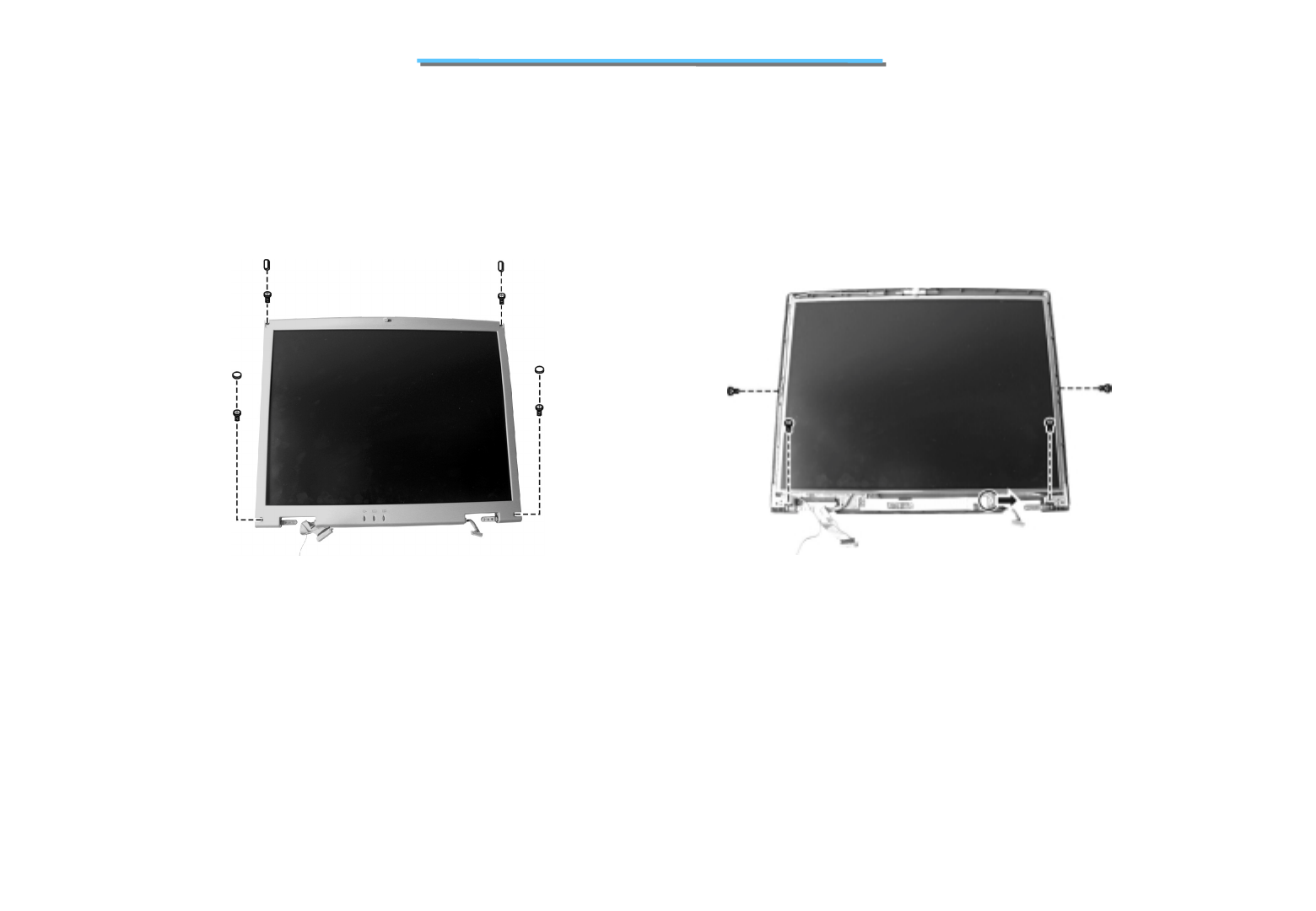
96
8170 N/B MAINTENANCE
Disassembly
1. Remove the LCD assembly. (See section 2.2.7 Disassembly.)
2. Remove the four rubber pads and four screws on the corners of the panel. (Figure 2-17)
Figure 2-17 Remove LCD frame Figure 2-18 Remove LCD panel
3. Insert a flat screwdriver to the lower part of the frame and gently pry the frame out.
Repeat the process until the frame is completely separated from the housing.
4. Remove the two screws on two sides and two screws on the lower part of of the LCD panel, and disconnect the
cable from the inverter board. (Figure 2-18)
Reassembly
1. Fit the LCD panel back into place and secure with four screws, and reconnect the cable to the inverter board.
2. Fit the LCD frame back into the housing and replace the four screws and four rubber pads.
3. Replace the LCD assembly. (See section 2.2.7 Reassembly.)
2.2.8 LCD Panel
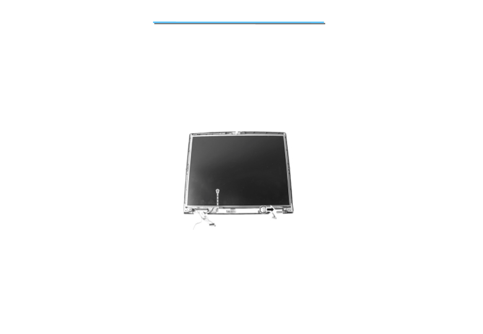
97
8170 N/B MAINTENANCE
Disassembly
1. Remove the LCD assembly. (see section 2.2.7 Disassembly. ).
2. Detach the LCD Panel. (See section 2.2.8 Disassembly. )
3. To remove the inverter board on the bottom of the LCD assembly, disconnect the cable and
remove one screw. (Figure 2-19)
Figure 2-19 Remove the Inverter Board
Reassembly
1. Fit the inverter board back into place and secure with one screw.
2. Reconnect the cable.
3. Replace the LCD frame. (See section 2.2.8 Reassembly.)
4. Replace the LCD assembly. (See section 2.2.7 Reassembly.)
2.2.9 Inverter Board
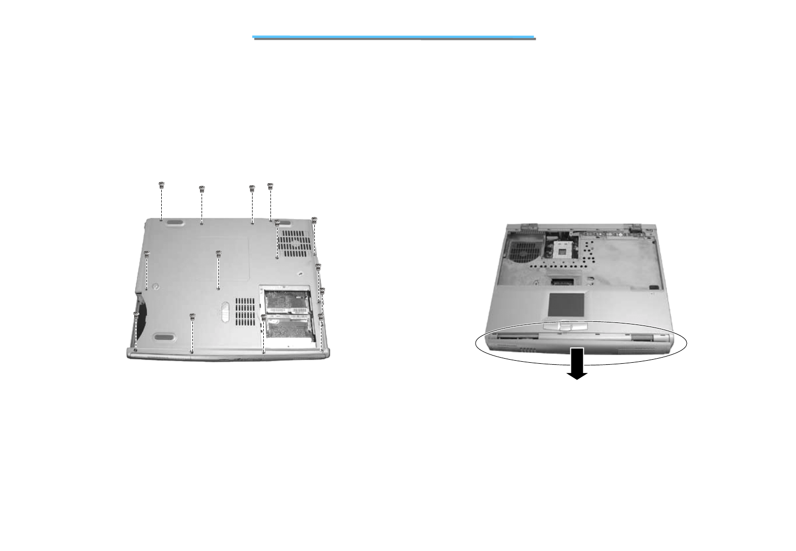
98
8170 N/B MAINTENANCE
Disassembly
1. Remove the battery pack, keyboard, CPU, HDD module, CD/DVD-ROM drive and LCD assembly.
(See sections2.2.1; 2.2.2; 2.2.3; 2.2.4; 2.2.5; 2.2.7 Disassembly.)
2. Remove fourteen screws on the bottom of the notebook. (Figure 2-20)
Figure 2-20 Remove the bottom Figure 2-21 Remove the speaker assembly
3. Remove the speaker assembly from the notebook. (Figure 2-21)
2.2.10 System Board
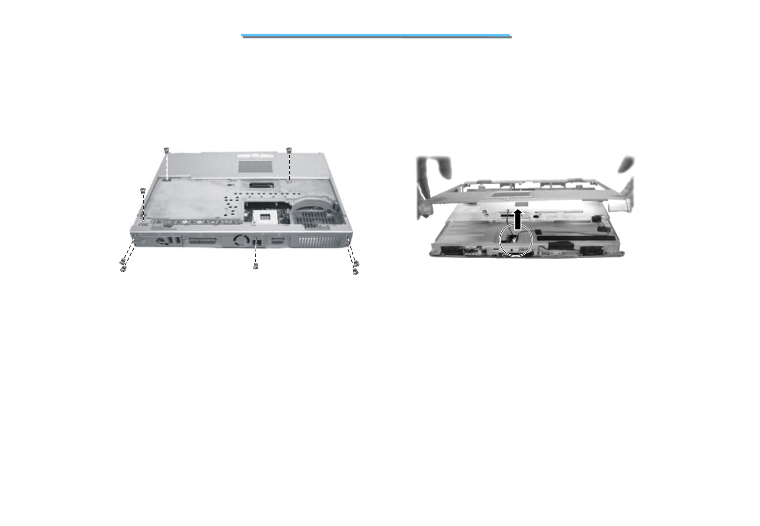
99
8170 N/B MAINTENANCE
4. Remove five screws on the rear side of the notebook, and remove three screws locking on the base unit cover.
(Figure 2-22)
Figure 2-22 Remove the base unit cover Figure 2-23 Lift up the base unit cover
5. Lift up the base unit cover and disconnect the touch pad cord. (Figure 2-23)
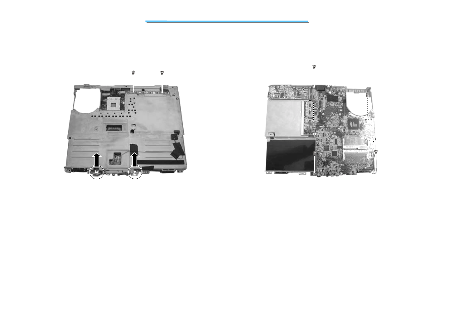
100
8170 N/B MAINTENANCE
6. Remove two screws fastening the button board on base unit. and then disconnect two cables from the
system board. (Figure 2-23)
Figure 2-23 Remove the screws Figure 2-24 Remove the base unit cover
7. Remove five screws from the system board,and lift up the base unit to access the system board. (Figure 2-24)
Reassembly
1. Replace five screws fastening the base unit
2. Reconnect two cables to the system board.
3. Replace the button board with two screws.
4. Reconnect the touch pad cable and replace the base unit cover.
5. Replace three screws fastening the base unit cover.
6. Replace five screws on the rear side of the notebook.

101
8170 N/B MAINTENANCE
7. Replace the speaker assembly.
8. Replace fourteen screws on the bottom of the notebook.
9. Replace the battery pack, LED panel, keyboard, CPU, HDD module, CD/DVD-ROM drive and LCD assembly.
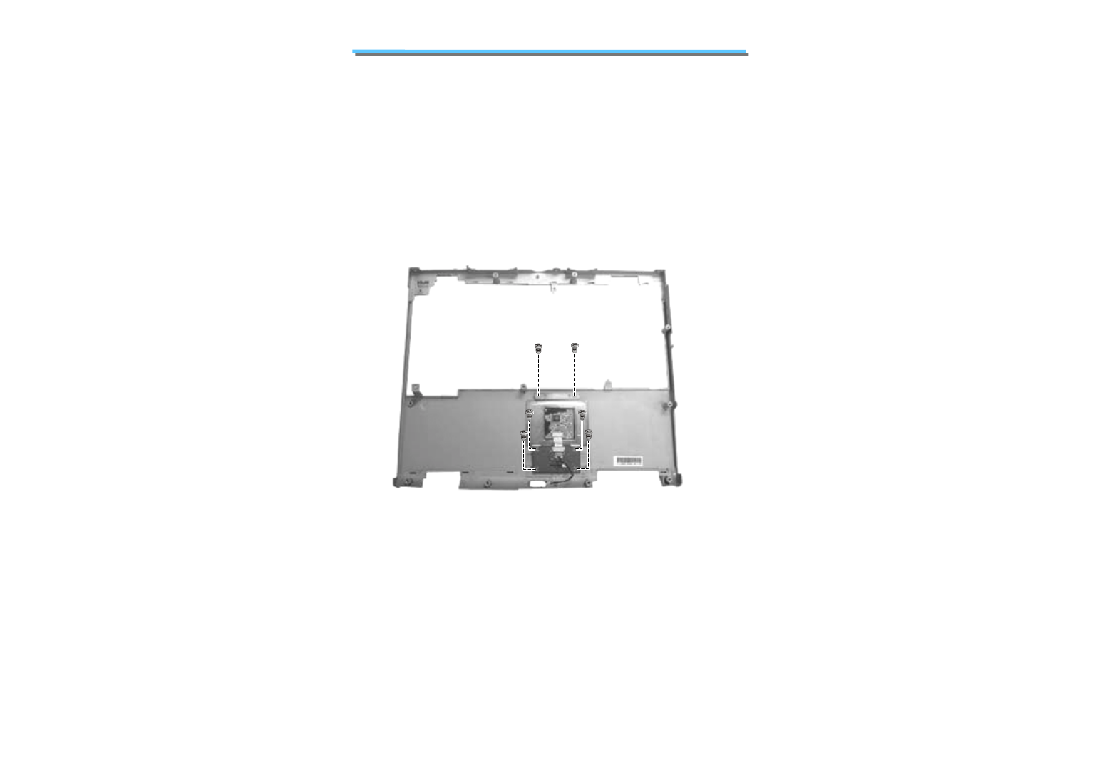
102
8170 N/B MAINTENANCE
Disassembly
1. Remove the base unit cover. (See steps 1-6 in section 2.2.11 Disassembly.)
2. Remove the six screws to lift up the touch pad holder and touch pad panel. (Figure 2-25)
Figure 2-25 Remove the touch pad
Reassembly
1. Replace the touch pad holder and touch pad panel, and secure with six screws.
2. Assemble the notebook. (See section 2.2.11 Reassembly.)
2.2.11 Touch PAD
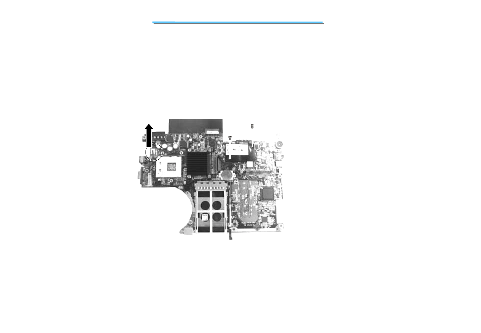
103
8170 N/B MAINTENANCE
Disassembly
1. Remove the battery pack, keyboard, CPU, HDD module, CD/DVD-ROM drive, and LCD assembly.
(See sections2.2.1; 2.2.2; 2.2.3; 2.2.4; 2.2.5; 2.2.7 Disassembly.)
3. Remove the two screws fastening the modem card,and then disconnect the cable from system board. (Figure 2-26)
Figure 2-26 Remove the Modem card
Reassembly
1. Reconnect the cable to the modem card and secure the modem card with two screws.
2. Assemble the notebook. (See section 2.2.10 Reassembly.)
2.2.12 Modem Card
2. Disassemble the notebook to access the system board. (See section 2.2.10 Disassembly.)
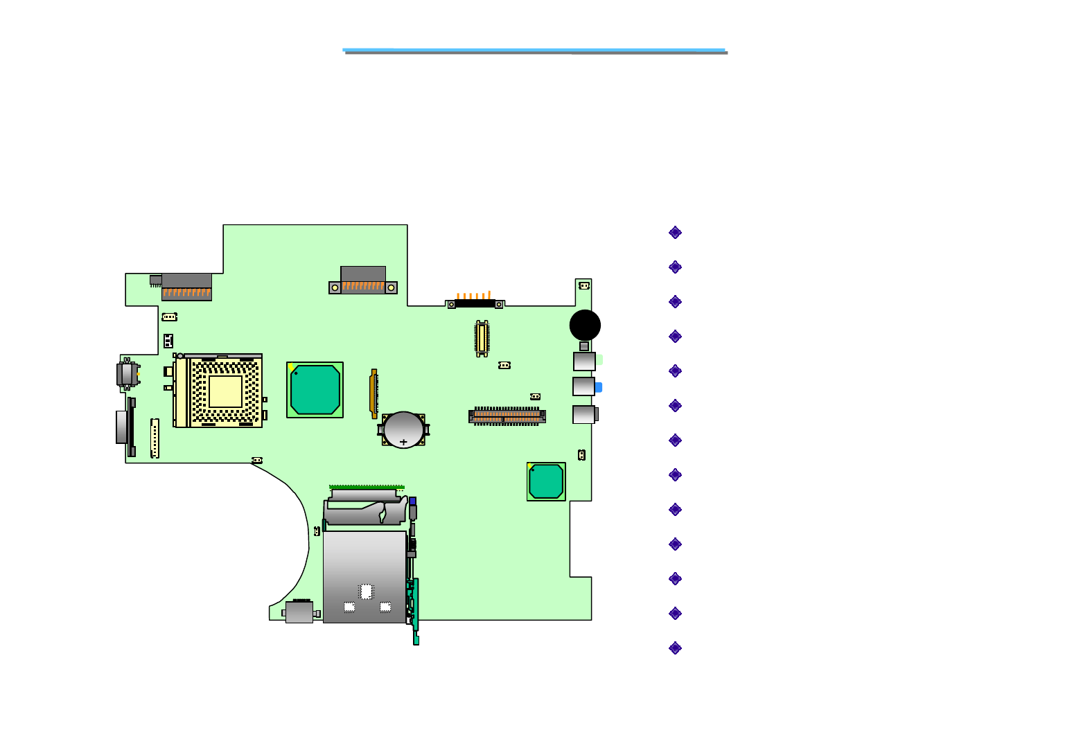
104
8170 N/B MAINTENANCE
3. Definition & Location Connectors / Switches Setting
3.1 Main Board ( Side A)
J1:External VGA Connector
J2:LCD Connector
J3:D/D Board connector
J4: Modem Daughter Board to RJ11Connector
J5:Easy Start Button Connector
J6:External USB(PIO,IR,TV OUT)Connector
J7:CPU FAN Connector
J8:Card Bus Socket
J9:RJ45
J10:Secondary EIDE Connector
J11:Modem Daughter Board
J12:Internal Keyboard Connector
J13:RJ11
J509
U1
J9
J20
VR1
SW6
J19
J22
J21
J18
J14
J16
J15
J11
J28
J10
J3
J6
J5
J4
J12
J2
J1
J13
J7
J8
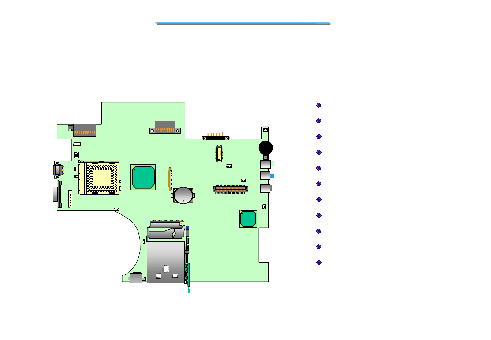
105
8170 N/B MAINTENANCE
3. Definition & Location Connectors / Switches Setting
3.1 Main Board ( Side A)
J14:Primary EIDE Connector
J15:Touch PAD Connector
J16:Internal Microphone
J18:Internal Speaker Connector(L channel)
J19:Line Out Phone Jack
J20:Internal Speaker Connector(R channel)
J21:Mini IEEE1394 Connector
J22:External Micro Phone Jack
J28:Battery Connector
VR1:Volume regulator
SW6:Switch Cover
J509
U1
J9
J20
VR1
SW6
J19
J22
J21
J18
J14
J16
J15
J11
J28
J10
J3
J6
J5
J4
J12
J2
J1
J13
J7
J8

106
8170 N/B MAINTENANCE
3. Definition & Location Connectors / Switches Setting
3.1 Main Board ( Side B )
J503
J505
U509
U508
U507 J502
U505
U504 U516
PU508
J502:D/D FAN connector
J503:DIMM1
J505:DIMM2
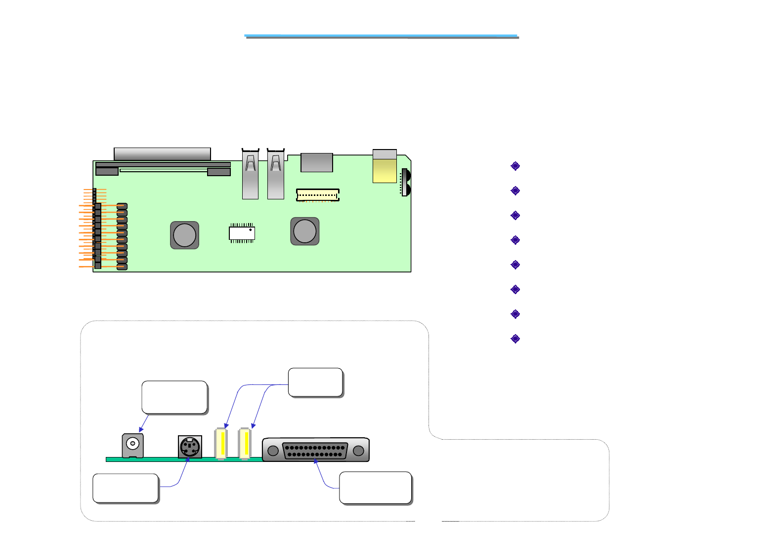
107
8170 N/B MAINTENANCE
3. Definition & Location Connectors / Switches Setting
3.2 D/D Board
J1:Parallel port connector
J2:USB2 connector
J3:USB0 connector
J4:TV Out connector
J5:Power Jack connector
J6:Inverter Board connector
PJ1:D/D Board connector
PJ2: External USB(PIO,IR,TV
OUT)Connector
J1
J2 J3
J4
J5 IR
PU1
PJ2
PJ1
J6
J5 J4 J3 J2 J1
Power Jack
connector
Power Jack
connector
TV Out
connector
TV Out
connector
USB0
connector
USB0
connector
Parallel port
connector
Parallel port
connector D/D Board Rear Side View
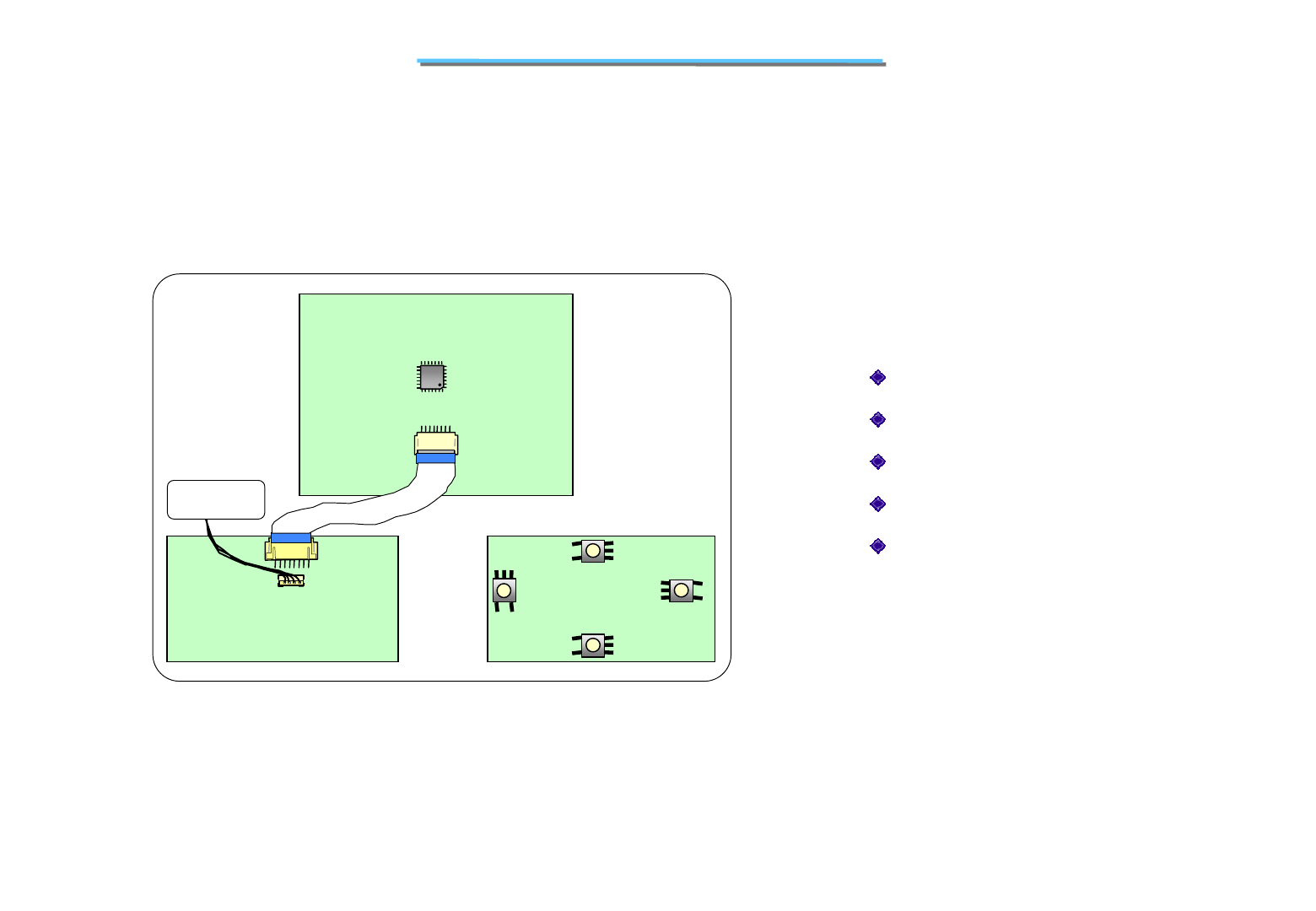
108
8170 N/B MAINTENANCE
3. Definition & Location Connectors / Switches Setting
3.3 Touch PAD Board
SW1:SCRL UP
SW2:RIGHT
SW3:LEFT
SW4:SCRL DOWN
J501:Touch PAD connector(to MB)
J500
J501
J1
U1
SW1
SW2
SW3
SW4
Connect to
MB J15

109
8170 N/B MAINTENANCE
4. Definition & Location Major Components
4.1 Main Board ( Side A )
J509
U1
U7
U17
U11
U12
U18
U13
U3
U4
U1:P4(Willamette/Northwood)Micro CPU
U3:82845 (Memory controller HUB)
U4:RTL8139CL(LANPHY)
U7:PCI4410(PCMCIA/1394 controller)
U11:74AHC373_V
U12:Flash Rom
U13:SN74CBTD3384(Level Shift)
U17:82801BA(I/O controller)
U18: Audio amplifier
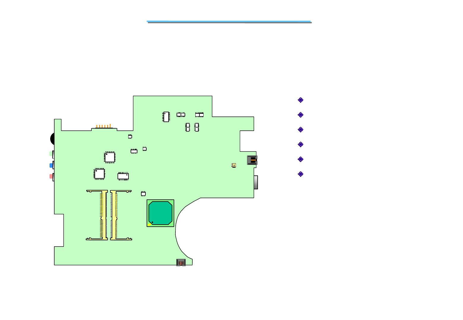
110
8170 N/B MAINTENANCE
4. Definition & Location Major Components
4.1 Main Board ( Side B )
U504:TPS2211
U507:ICS950805(Clock generator)
U508:Micro Controller(H8 F3437)
U509:PC87393(Supper I/O)
U516:ATI VGA controller
PU508:LTC1709EG-9(CPU_CORE regulator)
U509
U508
U507
J502
U504
U516
PU508
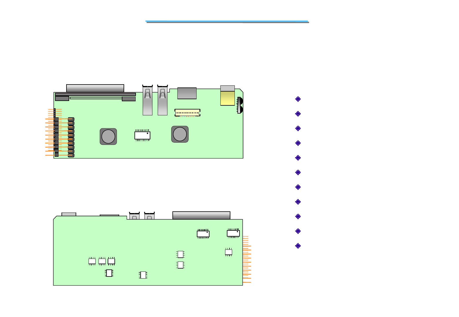
111
8170 N/B MAINTENANCE
4. Definition & Location Major Components
4.2 D/D Board
U501:PAC128401Q
U502:PAC128401Q
PU1:MAX1632(3V.5V.12V regulator)
PU501:AO4400
PU502:SI4832DY
PU503:SI4800DY
PU504:AO4400
PU505:SI4832Dy
PU506:SI4800Y
PQ502:SI4835DY
PQ503:SI4835DY
J1
J2 J3
J4
J5 IR
PU1
PJ2
PJ1
U502 U501
PU501
PU502
PU503
PU506 PU504
PQ503
PQ502
PU505
D/D Board (Side A)
D/D Board (Side B)
112
8170 N/B MAINTENANCE
5. Pin Descriptions of Major Components
5.1 Pentium 4(Willamette/Northwood) mFC-PGA2 478 pin
Name Type Description
A[35:3]# Input/
Output A[35:3]# (Address) define a 2 36 -byte physical memory address
space. In sub-phase 1 of the address phase, these pins transmit the
address of a transaction. In sub-phase 2, these pins transmit
transaction type information. These signals
must connect the appropriate pins of all agents on the Pentium 4
processor in the 478-pin package system bus. A[35:3]# are
protected by parity signals AP[1:0]#. A[35:3]# are source
synchronous signals and are latched into the receiving buffers by
ADSTB[1:0]#. On the active-to-inactive transition of RESET#, the
processor samples a subset of the A[35:3]# pins to determine
power-on configuration.
A20M# Input If A20M# (Address-20 Mask) is asserted, the processor masks
physical address bit 20 (A20#) before looking up a line in any
internal cache and before driving a read/write transaction on the
bus. Asserting A20M# emulates the 8086 processor's address
wrap-around at the 1-Mbyte boundary. Assertion of A20M# is only
supported in real mode.
A20M# is an asynchronous signal. However, to ensure recognition
of this signal following an Input/Output write instruction, it must be
valid along with the TRDY# assertion of the corresponding
Input/Output Write bus transaction.
ADS# Input/
Output ADS# (Address Strobe) is asserted to indicate the validity of the
transaction address on the A[35:3]# and REQ[4:0]# pins. All bus
agents observe the ADS# activation to begin parity checking,
protocol checking, address decode, internal snoop, or deferred reply
ID match operations associated with the new transaction.
ADSTB[1:0]# Input/
Output Address strobes are used to latch A[35:3]# and REQ[4:0]# on their
rising and falling edges. Strobes are associated with signals as
shown below.
Signals Associated Strobe
REQ[4:0]#, A[16:3]# ADSTB0#
A[35:17]# ADSTB1#
Name Type Description
AP[1:0]# Input/
Output AP[1:0]# (Address Parity) are driven by the request initiator along
with ADS#,A[35:3]#, and the transaction type on the REQ[4:0]#. A
correct parity signal is high if an even number of covered signals
are low and low if an odd number of covered signals are low. This
allows parity to be high when all the covered signals are high.
AP[1:0]# should connect the appropriate pins of all Pentium 4
processor in the 478-pin package system bus agents. The following
table defines
Request Signals subphase 1 subphase 2
A[35:24]# AP0# AP1#
A[23:3]# AP1# AP0#
REQ[4:0]# AP1# AP0#
BCLK[1:0] Input The differential pair BCLK (Bus Clock) determines the system bus
frequency. All processor system bus agents must receive these
signals to drive their outputs and latch their inputs.
All external timing parameters are specified with respect to the
rising edge of BCLK0 crossing V CROSS .
BINIT# Input/
Output BINIT# (Bus Initialization) may be observed and driven by all
processor system bus agents and if used, must connect the
appropriate pins of all such agents. If the BINIT# driver is enabled
during power-on configuration, BINIT# is asserted
to signal any bus condition that prevents reliable future operation.
If BINIT# observation is enabled during power-on configuration,
and BINIT# is sampled asserted, symmetric agents reset their bus
LOCK# activity and bus request arbitration state machines. The bus
agents do not reset their IOQ and transaction tracking state
machines upon observation of BINIT# activation. Once the BINIT#
assertion has been observed, the bus agents will re-arbitrate for the
system bus and attempt completion of their bus queue and IOQ
entries.
If BINIT# observation is disabled during power-on configuration, a
central agent may handle an assertion of BINIT# as appropriate to
the error handling architecture of the system.
BNR# Input/
Output
BNR# (Block Next Request) is used to assert a bus stall by any bus
agent who is unable to accept new bus transactions. During a bus
stall, the current bus owner cannot issue any new transactions.
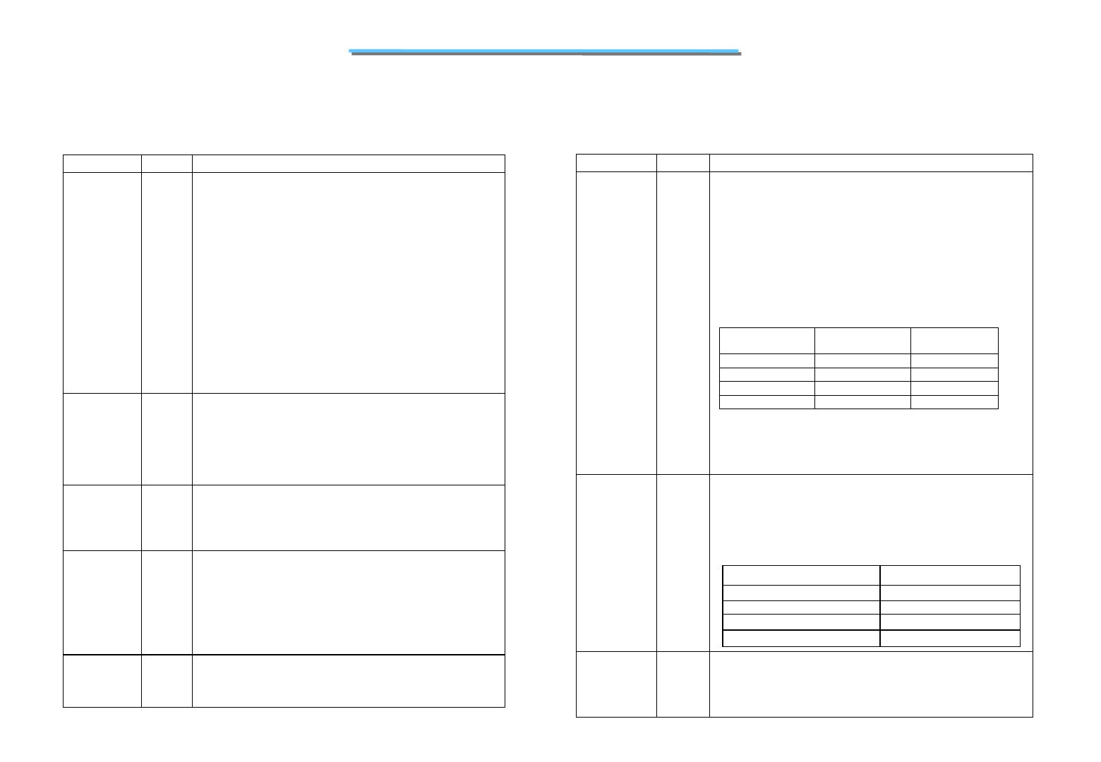
113
8170 N/B MAINTENANCE
Name Type Description
BPM[5:0]# Input/
Output BPM[5:0]# (Breakpoint Monitor) are breakpoint and performance
monitor signals. They are outputs from the processor which indicate
the status of breakpoints and programmable counters used for
monitoring processor performance. BPM[5:0]# should connect the
appropriate pins of all Pentium 4 processor in the 478-pin package
system bus agents.
BPM4# provides PRDY# (Probe Ready) functionality for the TAP
port. PRDY# is a processor output used by debug tools to determine
processor debug readiness.
BPM5# provides PREQ# (Probe Request) functionality for the TAP
port. PREQ# is used by debug tools to request debug operation of
the processor. Please refer to the Intel® Pentium® 4 Processor in
the 478-pin Package and Intel® 850 Chipset Platform Design
Guide for more detailed information.
These signals do not have on-die termination. the Intel®
Pentium® 4 Processor in the 478-pin Package and Intel® 850
Chipset Platform Design Guide for termination requirements.
BPRI# Input BPRI# (Bus Priority Request) is used to arbitrate for ownership of
the processor system bus. It must connect the appropriate pins of all
processor system bus agents. Observing BPRI# active (as asserted
by the priority agent) causes all other agents to stop issuing new
requests, unless such requests are part of an ongoing locked
operation. The priority agent keeps BPRI# asserted until all of its
requests are completed, then releases the bus by deasserting BPRI#.
BR0# Input/
Output BR0# drives the BREQ0# signal in the system and is used by the
processor to request the bus. During power-on configuration this pin
is sampled to determine the agent ID = 0.
This signal does not have on-die termination and must be
terminated.
BSEL[1:0] Output The BCLK[1:0] frequency select signals BSEL[1:0] are used to
select the processor input clock frequency. The required frequency
is determined by the processor, chipset and clock synthesizer. All
agents must operate at the same frequency. The Pentium 4
processor in the 478-pin package operates currently at a 400 MHz
system bus frequency (100 MHz BCLK[1:0] frequency). For more
information about these pins, including termination
recommendations.
COMP[1:0] Analog COMP[1:0] must be terminated on the system board using precision
resistors. Refer to the Intel® Pentium® 4 Processor in the 478-pin
Package and Intel® 850 Chipset Platform Design Guide for details
on implementation.
Name Type Description
D[63:0]# Input/
Output D[63:0]# (Data) are the data signals. These signals provide a 64-bit
data path between the processor system bus agents, and must
connect the appropriate pins on all such agents. The data driver
asserts DRDY# to indicate a valid data transfer.
D[63:0]# are quad-pumped signals and will thus be driven four
times in a common clock period. D[63:0]# are latched off the falling
edge of both DSTBP[3:0]# and DSTBN[3:0]#. Each group of 16
data signals correspond to a pair of one DSTBP# and one DSTBN#.
The following table shows the grouping of data signals to data
strobes and DBI#.
Quad-Pumped Signal Groups
Data Group DSTBN#/
DSTBP# DBI#
D[15:0]# 0 0
D[31:16]# 1 1
D[47:32]# 2 2
D[63:48]# 3 3
Furthermore, the DBI# pins determine the polarity of the data
signals. Each group of 16 data signals corresponds to one DBI#
signal. When the DBI# signal is active, the corresponding data
group is inverted and therefore sampled active high.
DBI[3:0]# Input/
Output DBI[3:0]# are source synchronous and indicate the polarity of the
D[63:0]# signals. The DBI[3:0]# signals are activated when the data
on the data bus is inverted. The bus agent will invert the data bus
signals if more than half the bits, within the covered group, would
change level in the next cycle.
DBI[3:0] Assignment To Data Bus
Bus Signal Data Bus Signals
DBI3# D[63:48]#
DBI2# D[47:32]#
DBI1# D[31:16]#
DBI0# D[15:0]#
DBR# Output DBR# is used only in processor systems where no debug port is
implemented on the system board. DBR# is used by a debug port
interposer so that an in-target probe can drive system reset. If a
debug port is implemented in the system, DBR# is a no connect in
the system. DBR# is not a processor signal.
5.1 Pentium 4(Willamette/Northwood) mFC-PGA2 478 pin
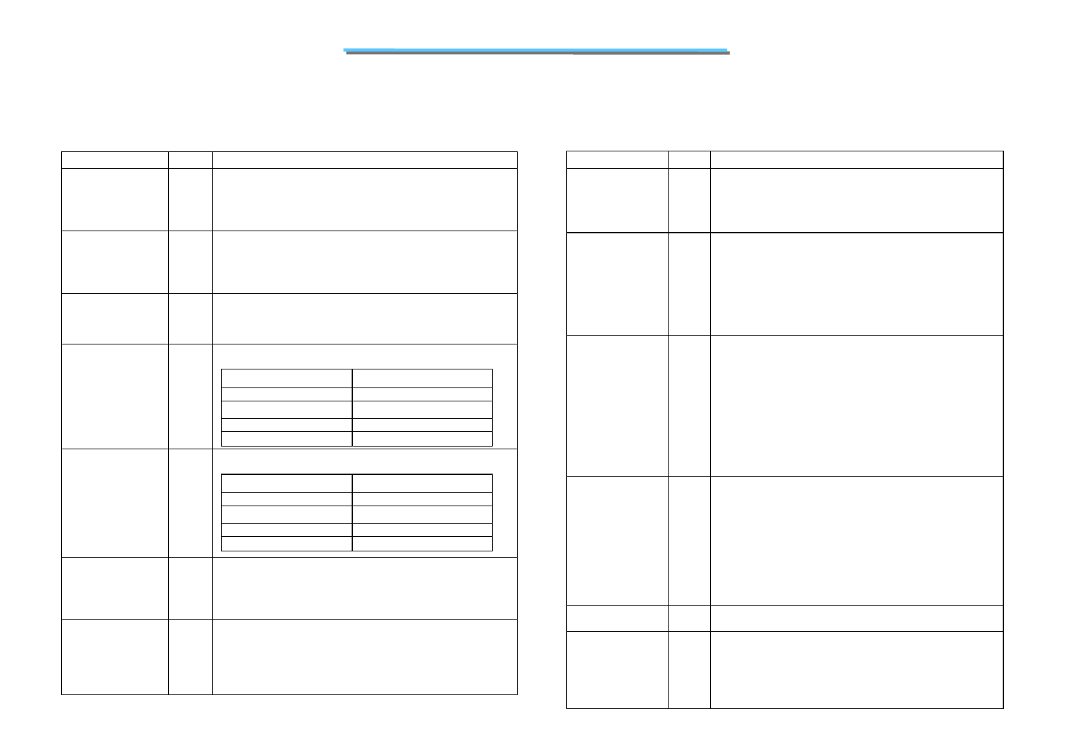
114
8170 N/B MAINTENANCE
5.1 Pentium 4(Willamette/Northwood) mFC-PGA2 478 pin
Name Type Description
DBSY#
Input/
Output
DBSY# (Data Bus Busy) is asserted by the agent responsible for
driving data on the processor system bus to indicate that the data
b
us is in use. The data bus isreleased after DBSY# is deasserted.
This signal must connect the appropriate pins on all processor
system bus agents.
DEFER#
Input
DEFER# is asserted by an agent to indicate that a transaction
cannot be guaranteed in-order completion. Assertion of
DEFER# is normally the responsibility of the addressed
memory or Input/Output agent. This signal must connect the
appropriate pins of all processor system bus agents.
DP[3:0]#
Input/
Output
DP[3:0]# (Data parity) provide parity protection for the
D[63:0]# signals. They are driven by the agent responsible for
driving D[63:0]#, and must connect the appropriate pins of all
Pentium 4 processor in the 478-pin package system bus gents.
DSTBN[3:0]#
Input/
Output
Data strobe used to latch in D[63:0]#.
Signals Associated Strobe
D[15:0]#, DBI0# DSTBN0#
D[31:16]#, DBI1# DSTBN1#
D[47:32]#, DBI2# DSTBN2#
D[63:48]#, DBI3# DSTBN3#
DSTBP[3:0]# Input/
Output
Data strobe used to latch in D[63:0]#.
Signals Associated Strobe
D[15:0]#, DBI0# DSTBP0#
D[31:16]#, DBI1# DSTBP1#
D[47:32]#, DBI2# DSTBP2#
D[63:48]#, DBI3# DSTBP3#
FERR#
Output
FERR# (Floating-point Error) is asserted when the processor
detects an unmasked floating-point error. FERR# is similar to
the ERROR# signal on the Intel 387 coprocessor, and is
included for compatibility with systems using MSDOS*-type
floating-point error reporting.
GTLREF
Input GTLREF determines the signal reference level for AGTL+ input
pins. GTLREF should be set at 2/3 VCC. GTLREF is used by the
AGTL+ receivers to determine if a signal is a logical 0 or
logical 1. Refer to the Intel® Pentium® 4 Processor in the
478-pin Package and Intel® 850 Chipset Platform Design
Guide for more information.
Name Type Description
HIT#
HITM# Input/
Output
Input/
Output
HIT# (Snoop Hit) and HITM# (Hit Modified) convey
transaction snoop operation results. Any system bus agent may
assert both HIT# and HITM# together to indicate that it requires
a snoop stall, which can be continued by reasserting
HIT# and HITM# together.
IERR#
Output IERR# (Internal Error) is asserted by a processor as the result of
an internal error. Assertion of IERR# is usually accompanied by
a SHUTDOWN transaction on the processor system bus. This
transaction may optionally be converted to an external error
signal (e.g., NMI) by system core logic. The processor will keep
IERR# asserted until the assertion of RESET#, BINIT#, or
INIT#.
This signals does not have on-die termination.
IGNNE#
Input IGNNE# (Ignore Numeric Error) is asserted to force the
processor to ignore a numeric error and continue to execute
noncontrol floating-point instructions. If IGNNE# is deasserted,
the processor generates an exception on a noncontrol
floating-point instruction if a previous floating-point instruction
caused an error.IGNNE# has no effect when the NE bit in
control register 0 (CR0) is set. IGNNE# is an asynchronous
signal. However, to ensure recognition of this signal following
an Input/Output write instruction, it must be valid along with the
TRDY# assertion of the corresponding Input/Output Write bus
transaction.
INIT#
Input INIT# (Initialization), when asserted, resets integer registers
inside the processor without affecting its internal caches or
floating-point registers. The processor then begins execution at
the power-on Reset vector configured during power-on
configuration. The processor continues to handle snoop requests
during INIT# assertion. INIT# is an asynchronous signal and
must connect the appropriate pins of all processor system bus
agents. If INIT# is sampled active on the active to inactive
transition of RESET#, then the processor executes its Built-in
Self-Test (BIST).
ITPCLKOUT[1:0]
Output
The ITPCLKOUT[1:0] pins do not provide any output for the
Pentium® 4 processor in the 478-pin package. Refer to
ITP_CLK[1:0]
Input ITP_CLK[1:0] are copies of BCLK that are used only in
processor systems where no debug port is implemented on the
system board. ITP_CLK[1:0] are used as BCLK[1:0] references
for a debug port implemented on an interposer. If a debug port
is implemented in the system, ITP_CLK[1:0] are no connects in
the system. These are not processor signals.
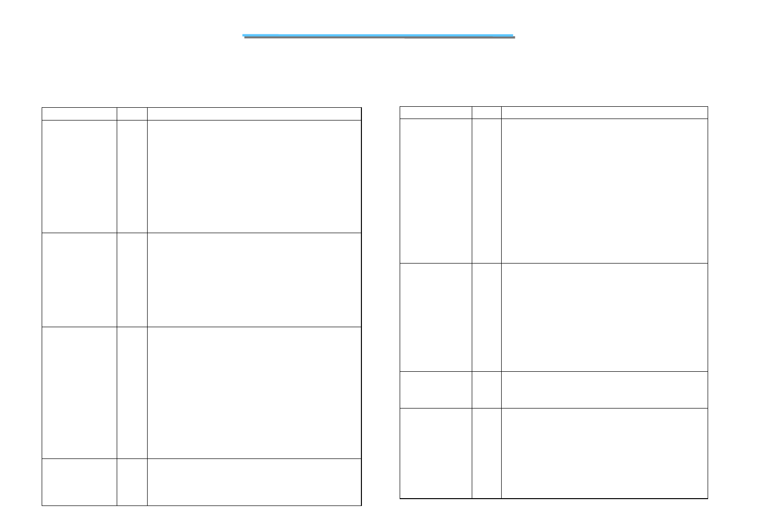
115
8170 N/B MAINTENANCE
5.1 Pentium 4(Willamette/Northwood) mFC-PGA2 478 pin
Name Type Description
LINT[1:0]
Input
LINT[1:0] (Local APIC Interrupt) must connect the appropriate
pins of all APIC Bus agents. When the APIC is disabled, the
LINT0 signal becomes INTR, a maskable interrupt request
signal, and LINT1 becomes NMI, a nonmaskable interrupt.
INTR and NMI are backward compatible with the signals of
those names on the Pentium processor. Both signals are
asynchronous.
Both of these signals must be software configured via BIOS
programming of the APIC register space to be used either as
NMI/INTR or LINT[1:0]. Because the APIC is enabled by
default after Reset, operation of these pins as LINT[1:0] is the
default configuration.
LOCK#
Input/
Output
LOCK# indicates to the system that a transaction must occur
atomically. This signal must connect the appropriate pins of all
processor system bus agents. For a locked sequence of
transactions, LOCK# is asserted from the beginning of the
first transaction to the end of the last transaction.
When the priority agent asserts BPRI# to arbitrate for ownership
of the processor system bus, it will wait until it observes
LOCK# deasserted. This enables symmetric agents to retain
ownership of the processor system bus throughout the bus
locked operation and ensure the atomicity of lock.
MCERR# Input/
Output
MCERR# (Machine Check Error) is asserted to indicate an
unrecoverable error without a bus protocol violation. It may be
driven by all processor system bus agents.
MCERR# assertion conditions are configurable at a system
level. Assertion options are defined by the following options:
Enabled or disabled.
Asserted, if configured, for internal errors along with IERR#.
Asserted, if configured, by the request initiator of a bus
transaction after it observes an error.
Asserted by any bus agent when it observes an error in a bus
transaction.
For more details regarding machine check architecture, please
refer to the IA-32 Software Developer’s Manual, Volume 3:
System Programming Guide.
PROCHOT#
Output
PROCHOT# will go active when the processor temperature
monitoring sensor detects that the processor has reached its
maximum safe operating temperature.
This indicates that the processor Thermal Control Circuit has
been activated, if enabled.
Name Type Description
PWRGOOD
Input
PWRGOOD (Power Good) is a processor input. The processor
requires this signal to be a clean indication that the clocks and
power supplies are stable and within their specifications.
‘Clean’ implies that the signal will remain low (capable of
sinking leakage current), without glitches, from the time that the
power supplies are turned on until they come within
specification. The signal must then transition monotonically to a
high illustrates the relationship of PWRGOOD to the RESET#
signal. PWRGOOD can be driven inactive at any time, but
clocks and power must again be stable before a subsequent
rising edge of PWRGOOD. It must also meet the minimum
pulse width and be followed by a 1 to 10 ms RESET# pulse.
The PWRGOOD signal must be supplied to the processor; it is
used to protect internal circuits against voltage sequencing
issues. It should be driven high
throughout boundary scan operation.
RESET#
Input
Asserting the RESET# signal resets the processor to a known
state and invalidates its internal caches without writing back any
of their contents. For a power-on Reset, RESET# must stay
active for at least one millisecond after VCC and BCLK have
reached their proper specifications. On observing active
RESET#, all system bus agents will deassert their outputs within
two clocks. RESET# must not be kept asserted for more than 10
ms while PWRGOOD is asserted.
A number of bus signals are sampled at the active-to-inactive
transition of RESET# for power-on configuration.
This signal does not have on-die termination and must be
terminated on the system board.
RS[2:0]#
Input
RS[2:0]# (Response Status) are driven by the response agent
(the agent responsible for completion of the current transaction),
and must connect the appropriate pins of all processor system
bus agents.
RSP#
Input
RSP# (Response Parity) is driven by the response agent (the
agent responsible for completion of the current transaction)
during assertion of RS[2:0]#, the signals for which RSP#
provides parity protection. It must connect to the appropriate
pins of all processor system bus agents.
A correct parity signal is high if an even number of covered
signals are low and low if an odd number of covered signals are
low. While RS[2:0]# = 000, RSP# is also high, since this
indicates it is not being driven by any agent guaranteeing
correct parity.
116
8170 N/B MAINTENANCE
5.1 Pentium 4(Willamette/Northwood) mFC-PGA2 478 pin
Name Type Description
REQ[4:0]#
Input/
Output
REQ[4:0]# (Request Command) must connect the appropriate
p
ins of all processor system bus agents. They are asserted by the
current bus owner to define the currently active transaction type.
These signals are source synchronous to ADSTB0#. Refer to the
AP[1:0]# signal description for a details on parity checking of
these signals.
SKTOCC#
Output
SKTOCC# (Socket Occupied) will be pulled to ground by the
processor. System board designers may use this pin to determine
if the processor is present.
SLP#
Input
SLP# (Sleep), when asserted in Stop-Grant state, causes the
processor to enter the Sleep state. During Sleep state, the
processor stops providing internal clock signals to all units,
leaving only the Phase-Locked Loop (PLL) still operating.
Processors in this state will not recognize snoops or interrupts.
The processor will recognize only assertion of the RESET#
signal, deassertion of SLP#, and removal of the BCLK input
while in Sleep state. If SLP# is deasserted, the processor exits
Sleep state and returns to Stop-Grant state, restarting its internal
clock signals to the bus and processor core units. If the BCLK
input is stopped while in the Sleep state the processor will exit
the Sleep state and transition to the Deep Sleep state.
SMI#
Input
SMI# (System Management Interrupt) is asserted
asynchronously by system logic. On accepting a System
Management Interrupt, the processor saves the current state and
enter System Management Mode (SMM). An SMI
Acknowledge transaction is issued, and the processor begins
program execution from the SMM handler.
If SMI# is asserted during the deassertion of RESET# the
processor will tristate its outputs.
STPCLK#
Input
STPCLK# (Stop Clock), when asserted, causes the processor to
enter a low power Stop-Grant state. The processor issues a
Stop-Grant Acknowledge transaction, and stops providing
internal clock signals to all processor core units except the
system bus and APIC units. The processor continues to snoop
bus transactions and service interrupts while in Stop-Grant state.
When STPCLK# is deasserted, the processor restarts its internal
clock to all units and resumes execution. The assertion of
STPCLK# has no effect on the bus clock; STPCLK# is an
asynchronous input.
TCK
Input
TCK (Test Clock) provides the clock input for the processor
Test Bus (also knownas the Test Access Port).
Name Type Description
TDI
Input
TDI (Test Data In) transfers serial test data into the processor.
TDI provides the serial input needed for JTAG specification
support.
TDO
Output
TDO (Test Data Out) transfers serial test data out of the
processor. TDO provides the serial output needed for JTAG
specification support.
TESTHI[12:8]
TESTHI[5:0]
Input
TESTHI[12:8] and TESTHI[5:0] must be connected to a VCC
power source through a resistor for proper processor operation.
THERMDA Other Thermal Diode Anode.
THERMDC Other Thermal Diode Cathode.
THERMTRIP#
Output
Assertion of THERMTRIP# (Thermal Trip) indicates the
processor junction temperature has reached a level beyond
which permanent silicon damage may occur. Measurement of
the temperature is accomplished through an internal thermal
sensor which is configured to trip at approximately 135°C.Upon
assertion of THERMTRIP#, the processor will shut off its
internal clocks (thus halting program execution) in an attempt to
reduce the processor junction temperature. To protect the
processor, its core voltage (VCC) must be removed following
the assertion of THERMTRIP#. Once activated,
THERMTRIP# remains latched until RESET# is asserted.
While the assertion of the RESET# signal will de-assert
THERMTRIP# , if the processor’s junction
temperature remains at or above the trip level, THERMTRIP#
will again be asserted after RESET# is de-asserted.
TMS
Input
TMS (Test Mode Select) is a JTAG specification support signal
used by debug tools.
TRDY# Input
TRDY# (Target Ready) is asserted by the target to indicate that
it is ready to receive a write or implicit writeback data transfer.
TRDY# must connect the appropriate pins of all system bus
agents.
TRST#
Input
TRST# (Test Reset) resets the Test Access Port (TAP) logic.
TRST# must be driven low during power on Reset. This can be
done with a 680 . pull-down resistor.
VCCA
Input
VCCA provides isolated power for the internal processor core
PLLs. Refer to the Intel® Pentium® 4 Processor in the 478-pin
Package and Intel® 850 Chipset Platform Design Guide for
complete implementation details.
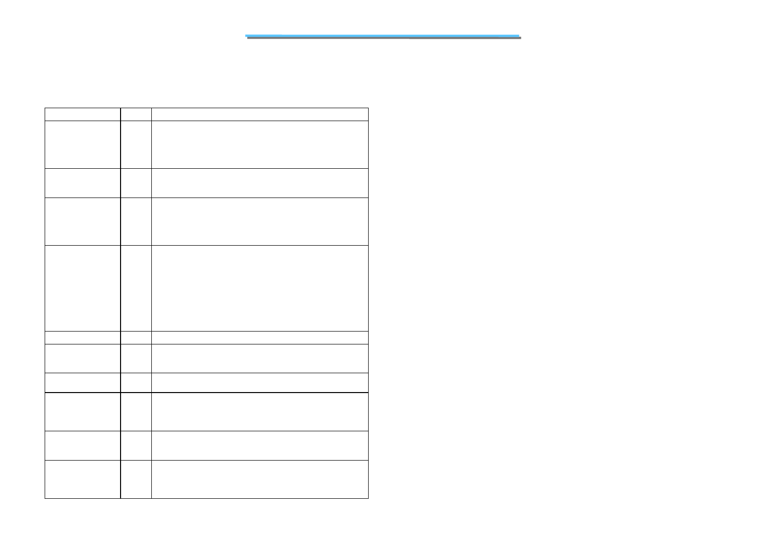
117
8170 N/B MAINTENANCE
5.1 Pentium 4(Willamette/Northwood) mFC-PGA2 478 pin
Name Type Description
VCCIOPLL
Input
VCCIOPLL provides isolated power for internal processor system
bus PLLs. Follow he guidelines for VCCA, and refer to the
I
ntel®
Pentium® 4 Processor in the 478-pin Package and Intel® 850
Chipset Platform Design Guide for complete implementation
details.
VCCSENSE
Output
VCCSENSE is an isolated low impedance connection to processor
core power(VCC). It can be used to sense or measure power near
the silicon with little noise.
VCCVID Input
There is no imput voltage requirement for VCCVID for designs
intended tosupport only the Pentium 4 processor in the 478-pin
package. Refer to the Intel® Pentium® 4 Processor in the
478-pin Package and Intel® 850 Chipset Platform Design
Guide for more information.
VID[4:0]
Output
VID[4:0] (Voltage ID) pins can be used to support automatic
selection of power supply voltages (Vcc). These pins are not
signals, but are either an open circuit or a short circuit to VSS
on the processor. The combination of opens and shorts
defines the voltage required by the processor. The VID pins are
needed to cleanly support processor voltage specification
variations. See 1.4 for definitions of these pins. The power
supply must supply the voltage that is requested by these pins,
or disable itself.
VSSA Input VSSA is the isolated ground for internal PLLs.
VSSSENSE Output
VSSSENSE is an isolated low impedance connection to processor
core VSS. It can be used to sense or measure ground near the
silicon with little noise
TMS Input TMS (Test Mode Select) is a JTAG specification support signal
used by debug tools.
TRDY# Input
TRDY# (Target Ready) is asserted by the target to indicate that
it is ready to receive a write or implicit writeback data transfer.
TRDY# must connect the appropriate pins of all system bus
agents.
TRST#
Input
TRST# (Test Reset) resets the Test Access Port (TAP) logic.
TRST# must be driven low during power on Reset. This can be
done with a 680 . pull-down resistor.
VCCA
Input
VCCA provides isolated power for the internal processor core
PLLs. Refer to the Intel® Pentium® 4 Processor in the 478-pin
Package and Intel® 850 Chipset Platform Design Guide for
complete implementation details.
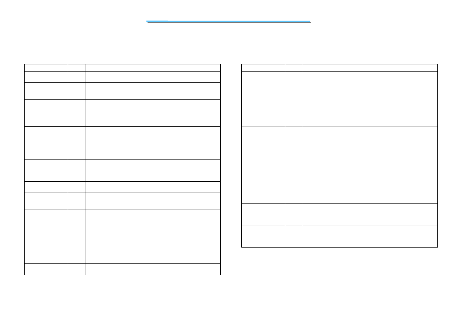
118
8170 N/B MAINTENANCE
5.2 Intel 82845(Brookdale Memory Controller HUB)
System Bus singnals
Name Type Description
ADS#
I/O
AGTL+ Address Strobe: The system bus owner asserts ADS# to indicate the
first of two cycles of a request phase.
BNR#
I/O
AGTL+
Block Next Request: BNR# is used to block the current request bus
owner from issuing a new request. This signal dynamically controls
the system bus pipeline depth.
BPRI#
O
AGTL+
Bus Priority Request: The MCH is the only Priority Agent on the
system bus. It asserts this signal to obtain the ownership of the
address bus. This signal has priority over symmetric bus requests and
will cause the current symmetric owner to stop issuing new
transactions unless the HLOCK# signal was asserted.
BR0#
I/O
AGTL+
Bus Request 0#: The MCH pulls the processor bus BR0# signal low
during CPURST#. The signal is sampled by the processor on the
active - to-inactive transition of CPURST#. The minimum setup time
for this signal is 4 BCLKs. The minimum hold time is 2 BCLKs and
the maximum hold time is 20 BCLKs. BR0# should be three-stated
after the hold time requirement has been satisfied.
CPURST#
O
AGTL+
Processor Reset: The CPURST# pin is an output from the MCH. The
MCH asserts CPURST# while RSTIN# (PCIRST# from the ICH2) is
asserted and for approximately 1 ms after RSTIN# is deasserted. The
CPURST# allows the processor to begin execution in a known state.
DBSY#
I/O
AGTL+ Data Bus Busy: DBSY# is used by the data bus owner to hold the
data bus for transfers requiring more than one cycle.
DEFER#
O
AGTL+
Defer Response: This signal, when asserted, indicates that the MCH
will terminate the transaction currently being snooped with either a
deferred response or with a retry response.
DBI[3:0]#
I/O
AGTL+
Dynamic Bus Inversion: DBI[3:0]# are driven along with the
HD[63:0]# signals. DBI[3:0]# Indicate if the associated data signals
are inverted. DBI[3:0]# are asserted such that the number of data bits
driven electrically low (low voltage) within the corresponding 16-bit
group never exceeds 8.
DBI[x]# Data Bits
DBI3# HD[63:48]#
DBI2# HD[47:32]#
DBI1# HD[31:16]#
DBI0# HD[15:0]#
DRDY# I/O
AGTL+ Data Ready. Asserted for each cycle that data is transferred.
Name Type Description
HA[31:3]#
I/O
AGTL+ Host Address Bus: HA[31:3]# connect to the system address bus.
During processor cycles, HA[31:3]# are inputs. The MCH drives
HA[31:3]# during snoop cycles on behalf of the hub interface and
AGP/Secondary PCI initiators. HA[31:3]# are transferred at 2x rate.
Note that the address is inverted on the system bus.
HADSTB[1:0]#
I/O
AGTL+ Host Address Strobe: The source synchronous strobes used to
transfer HA[31:3]# and HREQ[4:0]# at the 2x transfer rate.
Strobe Address Bits
HADSTB0# HA[16:3]#, HREQ[4:0]#
HADSTB1# HA[31:17]#
HD[63:0]#
I/O
AGTL+ Host Data: These signals are connected to the system data bus.
HD[63:0]# are transferred at a 4x rate. Note that the data signals are
inverted on the system bus.
HDSTBP[3:0]#
HDSTBN[3:0]#
I/O
AGTL+ Differential Host Data Strobes: The differential source synchronous
strobes used to transfer HD[63:0]# and DBI[3:0]# at the 4x transfer
rate.
Strobe Data Bits
HDSTBP3#, HDSTBN3# HD[63:48]#, DBI3#
HDSTBP2#, HDSTBN2# HD[47:32]#, DBI2#
HDSTBP1#, HDSTBN1# HD[31:16]#, DBI1#
HDSTBP0#, HDSTBN0# HD[15:0]#, DBI0#
HIT#
I/O
AGTL+ Hit: This signal indicates that a caching agent holds an unmodified
version of the requested line. HIT# is also driven in conjunction with
HITM# by the target to extend the snoop window.
HITM#
I/O
AGTL+ Hit Modified: This signal indicates that a caching agent holds a
modified version of the requested line and that this agent assumes
responsibility for providing the line. HITM# is also driven in
conjunction with HIT# to extend the snoop window.
HLOCK#
I/O
AGTL+ Host Lock: All system bus cycles sampled with the assertion of
HLOCK# and ADS#, until the negation of HLOCK# must be atomic
(i.e., no hub interface or AGP snoopable access to system memory are
allowed when HLOCK# is asserted by the processor).
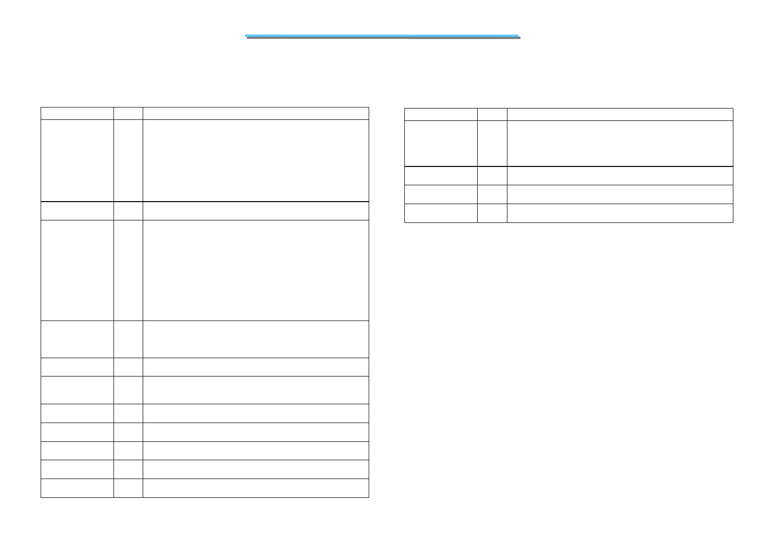
119
8170 N/B MAINTENANCE
5.2 Intel 82845(Brookdale Memory Controller HUB)
System Bus singnals
Name Type Description
HREQ[4:0]# I/O
AGTL+ Host Request Command: These signals define the attributes of the
request. In Enhanced Mode HREQ[4:0]# are transferred at 2x rate.
HREQ[4:0]# are asserted by the requesting agent during both halves
of Request Phase. In the first half the signals define the transaction
type to level of detail that is sufficient to begin a snoop request. In the
second half the signals carry additional information to define the
complete transaction type.
The transactions supported by the MCH host bridge are defined in the
Section 5.1.
HTRDY#
I/O
AGTL+ Host Target Ready: HTRDY# indicates that the target of the
processor transaction is able to enter the data transfer phase.
RS[2:0]#
O
AGTL+
Response Status: RS[2:0]# indicates the type of response according
to the following the table:
RS[2:0] Response Type
000 Idle state
001 Retry response
010 Deferred response
011 Reserved (not driven by MCH)
100 Hard Failure (not driven by MCH)
101 No data response
110 Implicit Write back
111 Normal data response
SCS[11:0]#
O
AGTL+
Chip Select: These signals select the particular SDRAM components
during the active state.
Note: There are two SCS# signals per SDRAM row. These signals
can be toggled on every rising system memory clock edge.
SMA[12:0]
O
AGTL+ Multiplexed Memory Address: These signals are used to provide
the multiplexed row and column address to SDRAM.
SBS[1:0]
O
AGTL+ Memory Bank Select: SBS[1:0] define the banks that are selected
within each SDRAM row. The SMA and SBS signals combine to
address every possible location in a SDRAM device.
SRAS#
O
AGTL+ SDRAM Row Address Strobe: SRAS# is Used with SCAS# and
SWE# (along with SCS#) to define the DRAM commands.
SCAS#
O
AGTL+ SDRAM Column Address Strobe: SCAS# is used with SRAS#
andSWE# (along with SCS#) to define the SDRAM commands.
SWE# O
AGTL+ Write Enable: SWE# is used with SCAS# and SRAS# (along with
SCS#) to define the SDRAM commands.
SDQ[63:0] I/O
AGTL+ Data Lines: These signals are used to interface to the SDRAM data
bus.
SCB[7:0] I/O
AGTL+ Check Bit Data Lines: These signals are used to interface to the
SDRAM ECC signals.
Name Type Description
SCKE[5:0]
O
AGTL+
Clock Enable: These pins are used to signal a self-refresh or
Powerdown command to a SDRAM array when entering system
suspend. SCKE is also used to dynamically powerdown inactive
SDRAM rows. There is one SCKE per SDRAM row. These signals
can be toggled on every rising SCLK edge.
RDCLKO
O
AGTL+ Clock Output: RDCLKO is used to emulate source-synch clocking
for reads. This signal connects to RDCLKIN.
SMA[12:0]
O
AGTL+ Multiplexed Memory Address: These signals are used to provide
the multiplexed row and column address to SDRAM.
RDCLKIN
I
AGTL+ Clock Input: RDCLKIN is used to emulate source-synch clocking
for reads. This signal connects to RDCLKO.
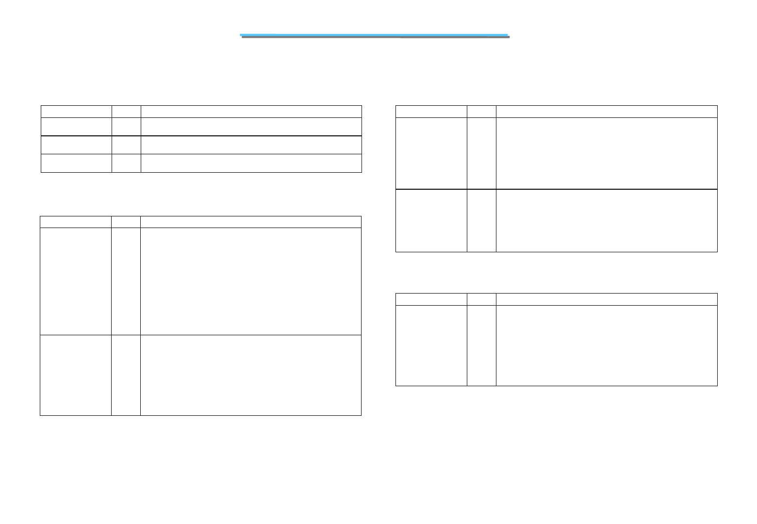
120
8170 N/B MAINTENANCE
5.2 Intel 82845(Brookdale Memory Controller HUB)
Hub Interface Signals
Name Type Description
HI_[10:0]
I/O
CMOS Hub Interface Signals: Signals used for the hub interface.
HI_STB
I/O
CMOS Hub Interface Strobe: One of two differential strobe signals used to
transmit or receive packet data over the hub interface.
HI_STB#
I/O
CMOS Hub Interface Strobe Compliment: One of two differential strobe
signals used to transmit or receive packet data over the hub interface.
AGP Addressing Signals
Name Type Description
PIPE#
I
AGP
Pipelined Read: This signal is asserted by the AGP master to
indicate a full-width address is to be enqueued on by the target using
the AD bus. One address is placed in the AGP request queue on each
rising clock edge while PIPE# is asserted. When PIPE# is deasserted,
no new requests are queued across the AD bus.
During SBA Operation: Not Used.
During FRAME# Operation: Not Used.
PIPE# is a sustained three-state signal from masters (graphics
controller), and is an MCH input.
Note: Initial AGP designs may not use PIPE# (i.e., PCI only 66
MHz). Therefore, an 8 k. pull-up resistor connected to this pin is
required on the motherboard.
SBA[7:0]
I
AGP
Sideband Address: These signals are used by the AGP master
(graphics controller) to place addresses into the AGP request queue.
The SBA bus and AD bus operate independently. That is, a
transaction can proceed on the SBA bus and the AD bus
simultaneously.
During PIPE# Operation: Not Used.
During FRAME# Operation: Not Used.
Note: When sideband addressing is disabled, these signals are
isolated (no external/internal pull-up resistors are required).
NOTE: The above table contains two mechanisms to queue requests by the AGP master. Note that
the master can only use one mechanism. The master may not switch methods without a full
reset of the system. When PIPE# is used to queue addresses the master is not allowed to
queue addresses using the SBA bus. For example, during configuration time, if the master
indicates that it can use either mechanism, the configuration software will indicate which
mechanism the master will use. Once this choice has been made, the master will continue to
use the mechanism selected until the master is reset (and reprogrammed) to use the other
mode. This change of modes is not a dynamic mechanism but rather a static decision when
the device is first being configured after reset.
AGP Flow Control Signals
Name Type Description
RBF#
I
AGP
Read Buffer Full: RBF# indicates if the master is ready to accept
previously requested low priority read data. When RBF# is asserted,
the MCH is not allowed to initiate the return low priority read data.
That is, the MCH can finish returning the data for the request
currently being serviced. RBF# is only sampled at the beginning of a
cycle. If the AGP master is always ready to accept return read data,
then it is not required to implement this signal.
During FRAME# Operation: Not Used.
WBF#
I
AGP
Write-Buffer Full: Indicates if the master is ready to accept fast
write data from the MCH. When WBF# is asserted, the MCH is not
allowed drive fast write data to the AGP master. WBF# is only
sampled at the beginning of a cycle. If the AGP master is always
ready to accept fast write data, then it is not required to implement
this signal.
During FRAME# Operation: Not Used.
AGP Status Signals
Name Type Description
ST[2:0]
O
AGP
Status: ST[2:0] provides information from the arbiter to an AGP
Master on what it may do. ST[2:0] only have meaning to the master
when its G_GNT# is asserted. When G_GNT# is deasserted, these
signals have no meaning and must be ignored. Refer to the AGP
Interface Specification, Revision 2.0 for further explanation of the
ST[2:0] values and their meanings.
During FRAME# Operation: These signals are not used during
FRAME#-based operation, except that a ¡¥111¡¦ indicates that the
master may begin a FRAME# transaction.
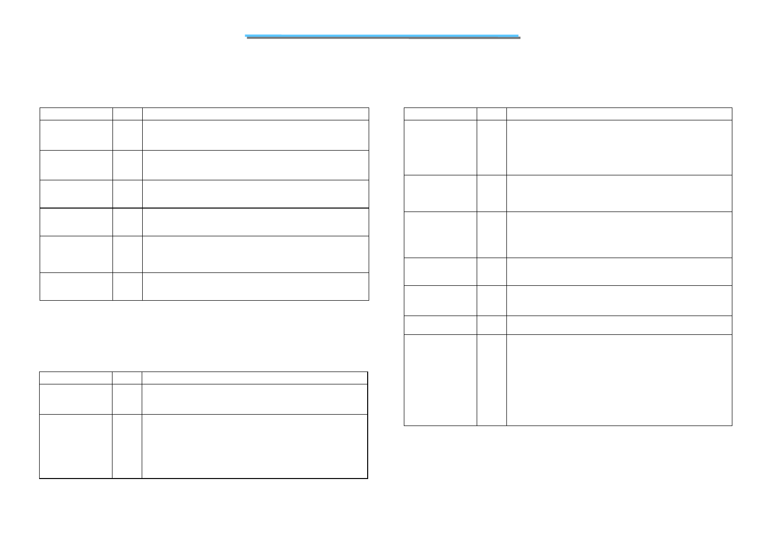
121
8170 N/B MAINTENANCE
5.2 Intel 82845(Brookdale Memory Controller HUB)
AGP Strobes Signals
Name Type Description
AD_STB0
I/O
(s/t/s)
AGP
Address/Data Bus Strobe-0: This signal provides timing for 2x and
4x data on AD[15:0] and the C/BE[1:0]# signals. The agent that is
providing the data drives this signal.
AD_STB0#
I/O
(s/t/s)
AGP
Address/Data Bus Strobe-0 Compliment: Differential strobe pair
that provides timing information for the AD[15:0] and C/BE[1:0]#
signals. The agent that is providing the data drives this signal.
AD_STB1
I/O
(s/t/s)
AGP
Address/Data Bus Strobe-1: This signal provides timing for 2x- and
4x-clocked data on AD[31:16] and C/BE[3:2]# signals. The agent that
is providing the data drives this signal.
AD_STB1#
I/O
(s/t/s)
AGP
Address/Data Bus Strobe-1 Compliment: The differential
compliment to the AD_STB1 signal. It is used to provide timing for
4x-clocked data.
SB_STB
I
AGP
Sideband Strobe: This signal provides timing for 2x- and 4x-
clocked data on the SBA[7:0] bus. It is driven by the AGP master
after the system has been configured for 2x- or 4x- clocked sideband
address delivery.
SB_STB#
I
AGP
Sideband Strobe Compliment: SB_STB# is the differential
compliment to the SB_STB signal. It is used to provide timing for
4x-clocked data.
AGP/PCISignals
For transactions on the AGP interface carried using AGP FRAME# protocol, these signals operate
similar to their semantics in the PCI 2.1 specification the exact role of all AGP FRAME# signals
are defined below.
Name Type Description
G_FRAME#
I/O
(s/t/s)
AGP
FRAME: During FRAME# Operations, G_FRAME# is an output
when the MCH acts as an initiator on the AGP Interface.
G_IRDY#
I/O
(s/t/s)
AGP
Initiator Ready#: This signal indicates the AGP compliant master is
ready to provide all write data for the current transaction. Once
G_IRDY# is asserted for a write operation, the master is not allowed
to insert wait states. The master is never allowed to insert a wait state
during the initial data transfer (32 bytes) of a write transaction.
However, it may insert wait states after each 32-byte block is
transferred.
Name Type Description
G_TRDY#
I/O
(s/t/s)
AGP
Target Ready: This signal indicates the AGP compliant target is
ready to
p
rovide read data for the entire transaction (when the transfer
size is less than or equal to 32 bytes) or is ready to transfer the initial
or subsequent block (32 bytes) of data when the transfer size is
greater than 32 bytes. The target is allowed to insert wait states after
each block (32 bytes) is transferred on write transactions.
G_STOP#
I/O
(s/t/s)
AGP
STOP: G_STOP Is an input when the MCH acts as a FRAME#-based
AGP initiator and an output when the MCH acts as a FRAME#-based
AGP target. G_STOP# is used for disconnect, retry, and abort
sequences on the AGP interface.
G_DEVSEL#
I/O
(s/t/s)
AGP
Device Select: This signal indicates that a FRAME#-based AGP
target device has decoded its address as the target of the current
access. The MCH asserts G_DEVSEL# based on the DRAM address
range being accessed by a PCI initiator. As an input it indicates
whether any device on the bus has been selected.
G_REQ#
I
AGP
Request: Indicates that a FRAME# or PIPE#-based AGP master is
requesting use of the AGP interface. This signal is an input into the
MCH.
G_GNT#
O
AGP
Grant: During SBA, PIPE# and FRAME# operation, G_GNT#,
along with the information on the ST[2:0] signals (status bus),
indicates how the AGP interface will be used next.
G_AD[31:0]
I/O
AGP Address/Data Bus: These signals are used to transfer both address
and data on the AGP interface.
G_C/BE[3:0]#
I/O
AGP
Command/Byte Enable:
During FRAME# Operation: During the address phase of a
transaction, G_C/BE[3:0]# define the bus command. During the data
phase, G_C/BE[3:0]# are used as byte enables. The byte enables
determine which byte lanes carry meaningful data.
During PIPE# Operation: When an address is enqueued using
PIPE#, the G_C/BE# signals carry command information. The
command encoding used during PIPE#-based AGP is DIFFERENT
than the command encoding used during FRAME#-
b
ased AGP cycles
(or standard PCI cycles on a PCI bus).
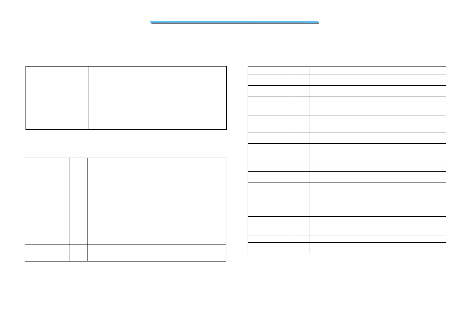
122
8170 N/B MAINTENANCE
5.2 Intel 82845(Brookdale Memory Controller HUB)
AGP/PCISignals
Name Type Description
G_PAR
I/O
AGP
Parity:
During FRAME# Operations: This signal is driven by the MCH
when it acts as a FRAME#-based AGP initiator during address and
data phases for a write cycle, and during the address phase for a read
cycle. PAR is driven by the MCH when it acts as a FRAME#-based
AGP target during each data phase of a FRAME#-based AGP
memory read cycle. Even parity is generated across AD[31:0] and
G_C/BE[3:0]#.
During SBA and PIPE# Operation: This signal is not used during
SBA and PIPE# operation.
Clocks, Reset, and Miscellaneous Signals
Name Type Description
BCLK
BCLK# I
CMOS
Differential Host Clock In: These pins receive a differential host
clock from the external clock synthesizer. This clock is used by all of
the MCH logic that is in the host clock domain.
66IN
I
CMOS
66 MHz Clock In: This pin receives a 66 MHz clock from the clock
synthesizer. This clock is used by AGP/PCI and hub interface clock
domains.
Note: That this clock input is 3.3 V tolerant.
SCK[11:0]
O
CMOS System Memory Clocks (SDR): These signals deliver a
synchronized clock to the DIMMs. There are two per row.
RSTIN#
I
CMOS
Reset In: When asserted, this signal asynchronously resets the MCH
logic. RSTIN# is connected to the PCIRST# output of the ICH2. All
AGP/PCI output and bi-directional signals will also three-state
compliant to PCI Rev 2.0 and 2.1 specifications.
Note: This input needs to be 3.3 V tolerant.
TESTIN#
I
CMOS
Test Input: This pin is used for manufacturing and board level test
purposes.
Note: This signal has an internal pull-up resistor.
Voltage Reference and Power Signals
Name Type Description
HVREF
Ref
Host Reference Voltage: Reference voltage input for the data,
address, and common clock signals of the host AGTL+ interface.
SDREF
Ref
SDRAM Reference Voltage: Reference voltage input for DQ, DQS,
RDCLKIN (SDR).
HI_REF Ref Hub Interface Reference: Reference voltage input for the hub
interface.
AGPREF Ref AGP Reference: Reference voltage input for the AGP interface.
HLRCOMP
I/O
CMOS
Compensation for Hub Interface: This signal is used to calibrate
the hub interface I/O buffers. It is connected to a 40.2 . pull-up
resistor with 1% tolerance and is pulled up to VCC1_8.
GRCOMP
I/O
CMOS Compensation for AGP: This signal is used to calibrate buffers. It is
connected to a 40.2 . pull-down resistor with a 1% tolerance.
HRCOMP[1:0]
I/O
CMOS
Compensation for Host: These signals are used to calibrate the host
AGTL+ I/O buffers. Each signal is connected to a 24.9 . pull-down
resistor with a 1% tolerance.
HSWNG[1:0]
I
CMOS Host Reference Voltage: Reference voltage input for the
compensation logic.
SMRCOMP
I/O
CMOS System Memory RCOMP:
VCC1_5
1.5 V Power Input: These pins are connected to a 1.5 V power
source.
VCC1_8
1.8 V Power Input Pins: These pins are connected to a 1.8 V power
source.
VCCSM
SDRAM Power Input Pins: These pins are connected to a 3.3 V
power source for SDR.
VCCA[1:0] PLL Power Input Pins: These pins provide power for the PLL.
VTT
AGTL+ Bus Termination Voltage Inputs: These pins provide the
AGTL+ bus termination.
VSS Ground: The VSS pins are the ground pins for the MCH.
VSSA[1:0]
PLL Ground: The VSSA[1:0] pins are the ground pins for the PLL
on the MCH.
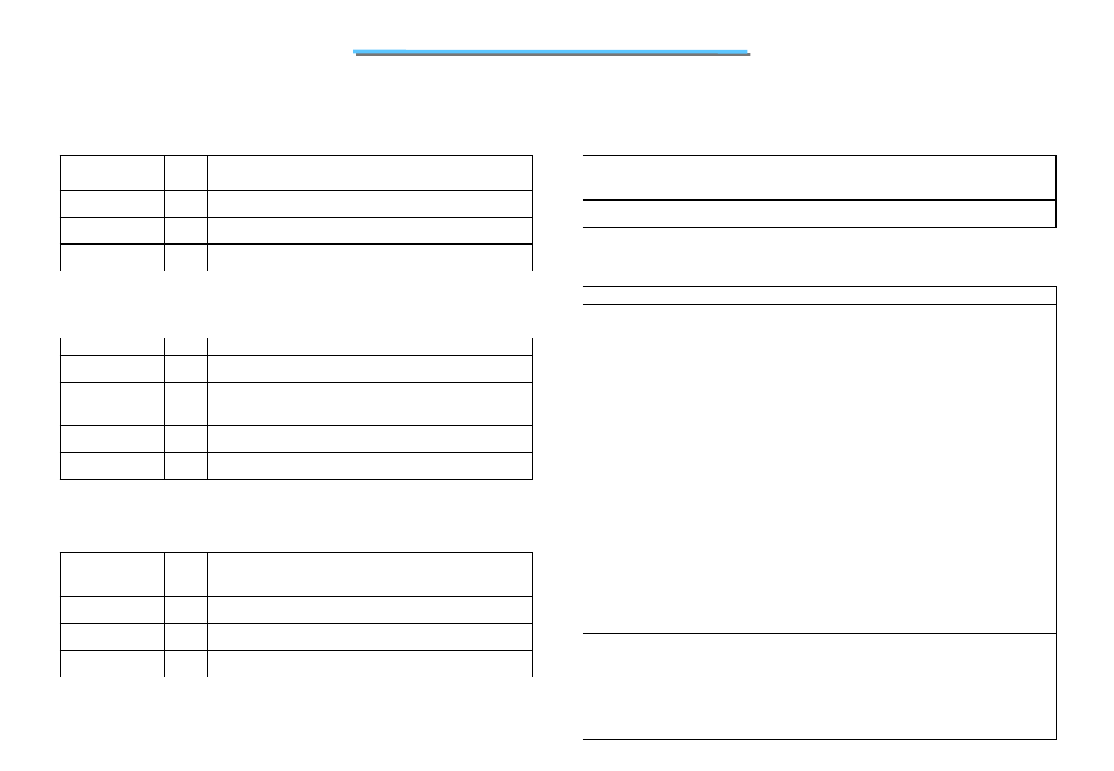
123
8170 N/B MAINTENANCE
5.3 Intel 82801BA(I/O Controller HUB )
Hub Interface Signals
Name Type Description
HL[11:0] I/O Hub Interface Signals
HL_STB
I/O
Hub Interface Strobe: One of two differential strobe signals used to
transmit and receive data through the hub interface.
HL_STB#
I/O
Hub Interface Strobe Complement: Second of the two differential
strobe signals.
HLCOMP
I/O
Hub Interface Compensation: Used for hub interface buffer
compensation.
LAN Connect Interface Signals
Name Type Description
LAN_CLK
I LAN Interface Clock: This signal is driven by the LAN Connect
component. The frequency range is 0.8 MHz to 50 MHz.
LAN_RXD[2:0]
I
Received Data: The LAN Connect component uses these signals to
transfer data and control information to the integrated LAN
Controller. These signals have integrated weak pull-up resistors.
LAN_TXD[2:0]
O
Transmit Data: The integrated LAN Controller uses these signals to
transfer data and control information to the LAN Connect component.
LAN_RSTSYNC
O
LAN Reset/Sync: The LAN Connect component’s Reset and Sync
signals are multiplexed onto this pin.
EEPROM Interface Signals
Name Type Description
EE_SHCLK
O EEPROM Shift Clock: EE_SHCLK is the serial shift clock output to
the EEPROM.
EE_DIN
I
EEPROM Data In: EE_DIN transfers data from the EEPROM to the
ICH2. This signal has an integrated pull-up resistor.
EE_DOUT
O
EEPROM Data Out: EE_DOUT transfers data from the ICH2 to the
EEPROM.
EE_CS
O
EEPROM Chip Select: EE_CS is a chip-select signal to the
EEPROM.
Firmware Hub Interface Signals
Name Type Description
FWH[3:0] /
LAD[3:0] I/O Firmware Hub Signals: These signals are muxed with LPC address
signals.
FWH[4] /
LFRAME# I/O
Firmware Hub Signals: This signal is muxed with LPC LFRAME#
signal.
PCI Interface Signals
Name Type Description
AD[31:0]
I/O PCI Address/Data: AD[31:0] is a multiplexed address and data bus.
During the first clock of a transaction, AD[31:0] contain a physical
address (32 bits). During subsequent clocks, AD[31:0] contain data.
The ICH2 drives all 0s on AD[31:0] during the address phase of all
PCI Special Cycles.
C/BE[3:0]#
I/O
Bus Command and Byte Enables: The command and byte enable
signals are multiplexed on the same PCI pins. During the address
phase of a transaction,C/BE[3:0]# define the bus command. During
the data phase, C/BE[3:0]# define the
Byte Enables.
C/BE[3:0]# Command Type
0000 Interrupt Acknowledge
0001 Special Cycle
0010 I/O Read
0011 I/O Write
0110 Memory Read
0111 Memory Write
1010 Configuration Read
1011 Configuration Write
1100 Memory Read Multiple
1110 Memory Read Line
1111 Memory Write and Invalidate
All command encodings not shown are reserved. The ICH2 does not
decode reserved values, and therefore will not respond if a PCI master
generates a cycle using one of the reserved values.
DEVSEL#
I/O
Device Select: The ICH2 asserts DEVSEL# to claim a PCI
transaction. As an output, the ICH2 asserts DEVSEL# when a PCI
master peripheral attempts an access to an internal ICH2 address or an
address destined for the hub interface (main memory or AGP). As an
input, DEVSEL# indicates the response to an ICH2- initiated
transaction on the PCI bus. DEVSEL# is tri-stated from the leading
edge of PCIRST#. DEVSEL# remains tri-stated by the ICH2 until
driven by a target device.
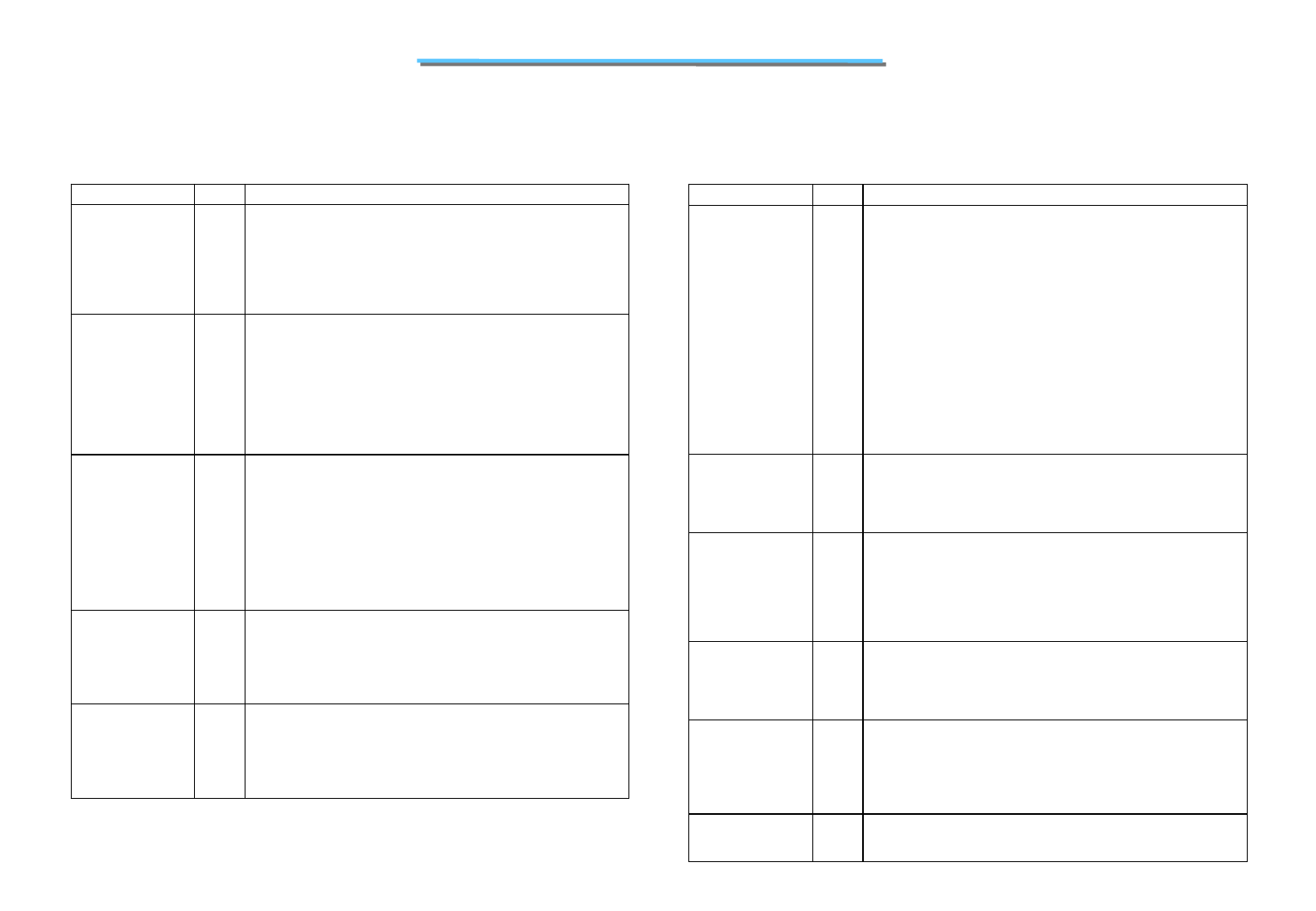
124
8170 N/B MAINTENANCE
5.3 Intel 82801BA(I/O Controller HUB )
PCI Interface Signals
Name Type Description
FRAME#
I/O Cycle Frame: The current Initiator drives FRAME# to indicate the
beginning and duration of a PCI transaction. While the initiator
asserts FRAME#, data transfers continue. When the initiator negates
FRAME#, the transaction is in the final data phase. FRAME# is an
input to the ICH2 when the ICH2 is the target, and FRAME# is an
output from the ICH2 when the ICH2 is the Initiator. FRAME#
remains tri-stated by the ICH2 until driven by an Initiator.
IRDY#
I/O
Initiator Ready: IRDY# indicates the ICH2's ability, as an Initiator,
to complete the current data phase of the transaction. It is used in
conjunction with TRDY#. A data phase is completed on any clock
both IRDY# and TRDY# are sampled asserted. During a write,
IRDY# indicates the ICH2 has valid data present on AD[31:0].
During a read, it indicates the ICH2 is prepared to latch data. IRDY#
is an input to the ICH2 when the ICH2 is the Target and an output
from the ICH2 when the ICH2 is an Initiator. IRDY# remains
tri-stated by the ICH2 until driven by an Initiator.
TRDY#
I/O
Target Ready: TRDY# indicates the ICH2's ability as a Target to
complete the current data phase of the transaction. TRDY# is used in
conjunction with IRDY#. A data phase is completed when both
TRDY# and IRDY# are sampled asserted. During a read, TRDY#
indicates that the ICH2, as a Target, has placed valid data on
AD[31:0]. During a write, TRDY# indicates the ICH2, as a Target is
prepared to latch data. TRDY# is an input to the ICH2 when the ICH2
is the Initiator and an output from the ICH2 when the ICH2 is a
Target. TRDY# is tri-stated from the leading edge of PCIRST#.
TRDY# remains tri-stated by the ICH2 until driven by a target.
STOP#
I/O
Stop: STOP# indicates that the ICH2, as a Target, is requesting the
Initiator to stop the current transaction. STOP# causes the ICH2, as an
Initiatior, to stop the current transaction. STOP# is an output when the
ICH2 is a target and an input when the ICH2 is an Initiator. STOP# is
tri-stated from the leading edge of PCIRST#. STOP# remains
tri-stated until driven by the ICH2.
REQ[0:4]#
REQ[5]# /
REQ[B]# /
GPIO[1]
I PCI Requests: The ICH2 supports up to 6 masters on the PCI bus.
REQ[5]# is muxed with PC/PCI REQ[B]# (must choose one or the
other, but not both). If not used for PCI or PC/PCI,
REQ[5]#/REQ[B]# can instead be used as GPIO[1].
Note: REQ[0]# is programmable to have improved arbitration latency
for supporting PCI-based 1394 controllers.
Name Type Description
PAR
I/O
Calculated/Checked Parity: PAR uses "even" parity calculated on
36 bits, AD[31:0] plus C/BE[3:0]#. "Even" parity means that the
ICH2 counts the number of 1s within the 36 bits plus PAR and the
sum is always even. The ICH2 always calculates PAR on 36 bits,
regardless of the valid byte enables. The ICH2 generates PAR for
address and data phases and only guarantees PAR to be valid one PCI
clock after the corresponding address or data phase. The ICH2 drives
and tri-states PAR identically to the AD[31:0] lines except that the
ICH2 delays PAR by exactly one PCI clock. PAR is an output during
the address phase (delayed one clock) for all ICH2 initiated
transactions. PAR is an output during the data phase (delayed one
clock) when the ICH2 is the Initiator of a PCI write transaction, and
when it is the target of a read transaction. ICH2 checks parity when it
is the target of a PCI write transaction. If a parity error is detected, the
ICH2 sets the appropriate internal status bits, and has the option to
generate an NMI# or SMI#.
PERR#
I/O
Parity Error: An external PCI device drives PERR# when it receives
data that has a
p
arity error. The ICH2 drives PERR# when it detects a
parity error. The ICH can either generate an NMI# or SMI# upon
detecting a parity error (either detected internally or reported via the
PERR# signal).
GNT[0:4]#
GNT[5]# /
GNT[B]# /
GPIO[17]#
O
PCI Grants: The ICH2 supports up to 6 masters on the PCI bus.
GNT[5]# is muxed with PC/PCI GNT[B]# (must choose one or the
other, but not both). If not needed PCI or PC/PCI, GNT[5]# can
instead be used as a GPIO.
Pull-up resistors are not required on these signals. If pullups are used,
they should be tied to the Vcc3_3 power rail.
GNT[B]#/GNT[5]#/GPIO[17] has an internal pullup.
PCICLK
I
PCI Clock: This is a 33 MHz clock. PCICLK provides timing for all
transactions on the PCI Bus. .
Note:For 82801BAM ICH2-M, this clock does not stop based on the
STP_PCI# signal. The PCI Clock only stops based on SLP_S1# or
SLP_S3#.
PCIRST#
O
PCI Reset: ICH2 asserts PCIRST# to reset devices that reside on the
PCI bus. The ICH2 asserts PCIRST# during power-up and when S/W
initiates a hard reset sequence through the RC (CF9h) register. The
ICH2 drives PCIRST# inactive a minimum of 1 ms after PWROK is
driven active. The ICH2 drives PCIRST# active a minimum of 1 ms
when initiated through the RC register.
SERR#
I System Error: SERR# can be pulsed active by any PCI device that
detects a system error condition. Upon sampling SERR# active, the
ICH2 has the ability to generate an NMI, SMI#, or interrupt.
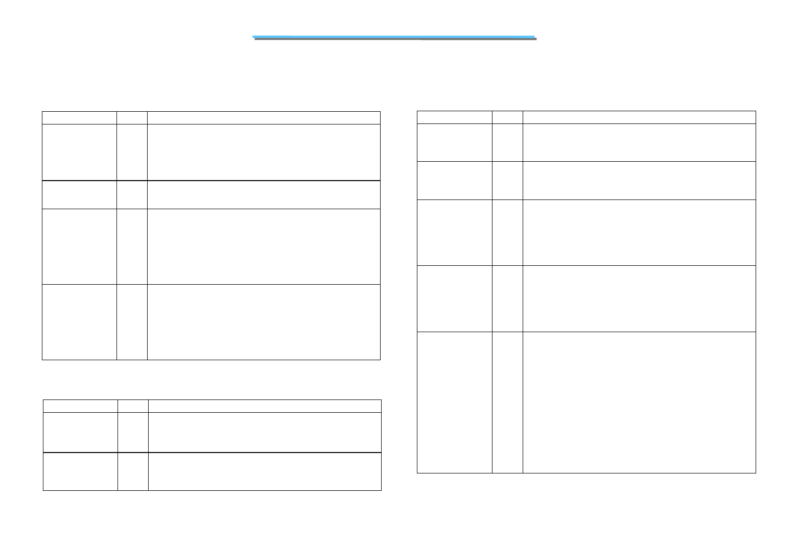
125
8170 N/B MAINTENANCE
5.3 Intel 82801BA(I/O Controller HUB )
PCI Interface Signals
Name Type Description
PME#
I
PCI Power Management Event: PCI peripherals drive PME# to
wake the system from low-power states S1–S5. PME# assertion can
also be enabled to generate SCI from the S0 state. In some cases the
ICH2 may drive PME# active due to an internal wake event. The
ICH2 will not drive PME# high, but it will be pulled up to VccSus3_3
by an internal pull-up resistor.
CLKRUN#
(ICH2-M only)
I/O
PCI Clock Run: For the ICH2-M, CLKRUN# is used to support PCI
Clock Run protocol. This signal connects to PCI devices that need to
request clock re-start or prevention of clock stopping.
REQ[A]# /
GPIO[0]
REQ[B]# /
REQ[5]# /
GPIO[1]
I
PC/PCI DMA Request [A:B]: This request serializes ISA-like DMA
Requests for the purpose of running ISA-compatible DMA cycles
over the PCI bus. This is used by devices such as PCI-based Super
I/O or audio codecs that need to perform legacy 8237 DMA but have
no ISA bus.
When not used for PC/PCI requests, these signals can be used as
General Purpose Inputs. Instead, REQ[B]# can be used as the 6th PCI
bus request.
GNT[A]# /
GPIO[16]
GNT[B]# /
GNT[5]# /
GPIO[17]
O
PC/PCI DMA Acknowledges [A:B]: This grant serializes an
ISA-like DACK# for the purpose of running DMA/ISA master cycles
over the PCI bus. This is used by devices such as PCI-
b
ased Super/IO
or audio codecs which need to perform legacy 8237 DMA but have
no ISA bus.
When not used for PC/PCI, these signals can be used as General
Purpose Outputs. GNTB# can also be used as the 6th PCI bus master
grant output. These signal have internal pull-up resistors.
IDE Interface Signals
Name Type Description
PDCS1#,
SDCS1#
O
Primary and Secondary IDE Device Chip Selects for 100 Range:
These signals are for the ATA command register block. This output
signal is connected to the corresponding signal on the primary or
secondary IDE connector.
PDCS3#,
SDCS3#
O
Primary and Secondary IDE Device Chip Select for 300 Range:
These signals are for the ATA control register block. This output
signal is connected to the corresponding signal on the primary or
secondary IDE connector.
IDE Interface Signals(continued)
Name Type Description
PDA[2:0],
SDA[2:0]
O
Primary and Secondary IDE Device Address: These output signals
are connected to the corresponding signals on the primary or
secondary IDE connectors. They are used to indicate which byte in
either the ATA command block or control block is being addressed.
PDD[15:0],
SDD[15:0]
I/O
Primary and Secondary IDE Device Data: These signals directly
drive the corresponding signals on the primary or secondary IDE
connector. There is a weak internal pull-down resistor on PDD[7] and
SDD[7].
PDDREQ,
SDDREQ
I
Primary and Secondary IDE Device DMA Request: These input
signals are directly driven from the DRQ signals on the primary or
secondary IDE connector. It is asserted by the IDE device to request a
data transfer, and used in conjunction with the PCI bus master IDE
function. They are not associated with
any AT-compatible DMA channel. There is a weak internal
pull-down resistor on these signals.
PDDACK#,
SDDACK#
O Primary and Secondary IDE Device DMA Acknowledge: These
signals directly drive the DAK# signals on the primary and secondary
IDE connectors. Each signal is asserted by the ICH2 to indicate to the
IDE DMA slave devices that a given data transfer cycle (assertion of
DIOR# or DIOW#) is a DMA data transfer cycle. This signal is used
in conjunction with the PCI bus master IDE function and are not
associated with any AT-compatible DMA channel.
PDIOR#
SDIOR#
O Primary and Secondary Disk I/O Read (PIO and Non-Ultra
DMA): This is the command to the IDE device that it may drive data
on the PDD or SDD lines. Data is latched by the ICH2 on the
deassertion edge of PDIOR# or SDIOR#. The IDE device is selected
either by the ATA register file chip selects (PDCS1# or SDCS1#,
PDCS3# or SDCS3#) and the PDA or SDA lines, or the IDE DMA
acknowledge (PDDAK# or SDDAK#).
Primary and Secondary Disk Write Strobe (Ultra DMA Writes to
Disk): This is the data write strobe for writes to disk. When writing to
disk, ICH2 drives valid data on rising and falling edges of PDWSTB
or SDWSTB.
Primary and Secondary Disk DMA Ready (Ultra DMA Reads
from Disk): This is the DMA ready for reads from disk. When
reading from disk, ICH2 deasserts PRDMARDY# orSRDMARDY#
to pause burst data transfers.
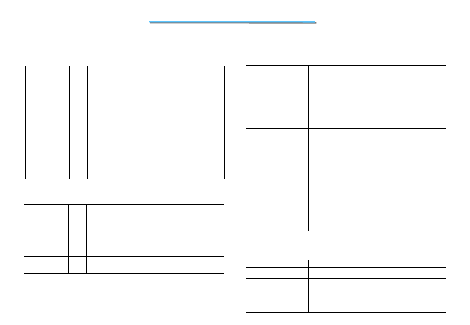
126
8170 N/B MAINTENANCE
5.3 Intel 82801BA(I/O Controller HUB )
IDE Interface Signals(continued)
Name Type Description
PDIOW#
SDIOW# O Primary and Secondary Disk I/O Write (PIO and Non-Ultra
DMA): This is the command to the IDE device that it may latch data
from the PDD or SDD lines. Data is latched by the IDE device on the
deassertion edge of PDIOW# or SDIOW#. The IDE device is selected
either by the ATA register file chip selects (PDCS1# or SDCS1#,
PDCS3# or SDCS3#) and the PDA or SDA lines, or the IDE DMA
acknowledge (PDDAK# or SDDAK#).
Primary and Secondary Disk Stop (Ultra DMA): ICH2 asserts this
signal to terminate a burst.
PIORDY
SIORDY
I Primary and Secondary I/O Channel Ready (PIO): This signal
keeps the strobe active (PDIOR# or SDIOR# on reads, PDIOW# or
SDIOW# on writes) longer than the minimum width. It adds wait
states to PIO transfers.
Primary and Secondary Disk Read Strobe (Ultra DMA Reads
from Disk): When reading from disk, ICH2 latches data on rising and
falling edges of this signal from the disk.
Primary and Secondary Disk DMA Ready (Ultra DMA Writes to
Disk): When writing to disk, this is deasserted by the disk to pause
burst data transfers
LPC Interface Signals
Name Type Description
LAD[3:0] /
FWH[3:0] I/O LPC Multiplexed Command, Address, Data: Internal pull-ups are
provided.
LFRAME# /
FWH[4] O LPC Frame: LFRAME# indicates the start of an LPC cycle, or an
abort.
LDRQ[1:0]#
O LPC Serial DMA/Master Request Inputs: These signals are used to
request DMA or bus master access. Typically, they are connected to
external Super I/O device. An internal pull-up resistor is provided on
these signals.
Interrupt Signals
Name Type Description
SERIRQ
I/O Serial Interrupt Request: This pin implements the serial interrupt
protocol.
PIRQ[D:A]#
I/OD
PCI Interrupt Requests: In Non-APIC Mode the PIRQx# signals
can be routed to interrupts 3:7, 9:12, 14, or 15 as described in the
Interrupt Steering section. Each PIRQx# line has a separate Route
Control Register.
In APIC mode, these signals are connected to the internal I/O APIC in
the following fashion: PIRQ[A]# is connected to IRQ16, PIRQ[B]# to
IRQ17, PIRQ[C]# to IRQ18, and PIRQ[D]# to IRQ19. This frees the
ISA interrupts.
PIRQ[H]#,
PIRQ[G:F]#
GPIO[4:3],
PIRQ[E]#
I/OD
PCI Interrupt Requests: In Non-APIC Mode the PIRQx# signals
can be routed to interrupts 3:7, 9:12, 14 or 15 as described in the
Interrupt Steering section. Each PIRQx# line has a separate Route
Control Register.
In APIC mode, these signals are connected to the internal I/O APIC in
the following fashion: PIRQ[E]# is connected to IRQ20, PIRQ[F]# to
IRQ21, PIRQ[G]# to IRQ22, and PIRQ[H]# to IRQ23. This frees the
ISA interrupts. If not needed for interrupts, PIRQ[G:F] can be used as
GPIO.
IRQ[14:15]
I Interrupt Request 14:15: These interrupt inputs are connected to the
IDE drives. IRQ14 is used by the drives connected to the primary
controller and IRQ15 is used
b
y the drives connected to the secondary
controller.
APICCLK I APIC Clock: The APIC clock runs at 33.333 MHz.
APICD[1:0]
I/OD
APIC Data: These bi-directional open drain signals are used to send
and receive data over the APIC bus. As in
p
uts, the data is valid on the
rising edge of APICCLK.As outputs, new data is driven from the
rising edge of the APICCLK.
USB Interface Signals
Name Type Description
USBP0P,
USBP0N,
USBP1P,
USBP1N
I/O
Universal Serial Bus Port 1:0 Differential: These differential pairs
are used to transmit Data/Address/Command signals for ports 0 and 1
(USB Controller 1).
USBP2P,
USBP2N,
USBP3P,
USBP3N
I/O
Universal Serial Bus Port 3:2 Differential: These differential pairs
are used to transmit Data/Address/Command signals for ports 2 and 3
USB Controller 2).
OC[3:0]#
I
Overcurrent Indicators: These signals set corresponding bits in the
USB controllers to indicate that an overcurrent condition has
occurred.
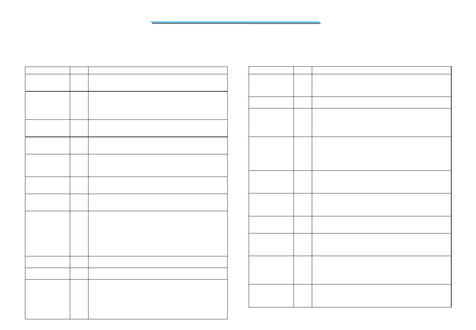
127
8170 N/B MAINTENANCE
5.3 Intel 82801BA(I/O Controller HUB )
Power Management Interface Signals
Name Type Description
THRM#
I
Thermal Alarm: THRM# is an active low signal generated by
external hardware to start the hardware clock throttling mode. This
signal can also generate an SMI# or an SCI.
SLP_S1#
(ICH2-M only)
O
S1 Sleep Control: Clock synthesizer or power plane control. This
signal connects to clock synthesizer’s PWRDWN# signal. An
optional use is to shut off power to non-critical systems when in the
S1 (Powered On Suspend), S3 (Suspend To RAM), S4 (Suspend to
Disk), or S5 (Soft Off) states.
SLP_S3#
O
S3 Sleep Control: Power plane control. This signal is used to shut off
power to all non-critical systems when in S3 (Suspend To RAM), S4
(Suspend to Disk) or S5 (Soft Off) states.
SLP_S5#
O S5 Sleep Control: Power plane control. This signal is used to shut
power off to all non-critical systems when in the S4 (Suspend To
Disk) or S5 (Soft Off) states.
PWROK
I Power OK: When asserted, PWROK is an indication to the ICH2
that core power and PCICLK have been stable for at least 1 ms.
PWROK can be driven asynchronously. When PWROK is negated,
the ICH2 asserts PCIRST#.
RSM_PWROK
(ICH2 0nly)
I Resume Well Power OK: When asserted, this signal is an indication
to the ICH2 that the resume well power (VccSus3_3, VccSus1_8) has
been stable for at least10 ms.
LAN_PWROK
(ICH2-M only)
I LAN Power OK: When asserted, this signal is an indication to the
ICH2-M that the LAN Controller power (VccLAN3_3, VccLAN1_8)
has been stable for at least 10 ms.
PWRBTN#
I Power Button: The Power Button will cause SMI# or SCI to indicate
a system request to go to a sleep state. If the system is already in a
sleep state, this signal will cause a wake event. If PWRBTN# is
pressed for more than 4 seconds, this will cause an unconditional
transition (power button override) to the S5 state with only the
PWRBTN# available as a wake event. Override will occur even if the
system is in the S1-S4 states. This signal has an internal pull-up
resistor.
RI#
I Ring Indicate: From the modem interface. This signal can be enabled
as a wake event; this is preserved across power failures.
RSMRST#
I Resume Well Reset: RSMRST# is used for resetting the resume
power plane logic.
SUS_STAT# /
LPCPD#
O Suspend Status: This signal is asserted by the ICH2 to indicate that
the system will be entering a low power state soon. This can be
monitored by devices with memory that need to switch from normal
refresh to suspend refresh mode. It can also be used by other
peripherals as an indication that they should isolate their outputs that
may be going to powered-off planes. This signal is called LPCPD# on
the LPC interface.
Name Type Description
C3_STAT# /
GPIO[21]
ICH2-M only)
O
C3_STAT#: This ICH2-M signal is typically configured as
C3_STAT#. It is used for indicating to an AGP device that a C3 state
transition is beginning or ending. If C3_STAT# functionality is not
required, this signal can be used as a GPO.
SUSCLK
O
Suspend Clock: This signal is an output of the RTC generator circuit
and is used by other chips for the refresh clock.
VRMPWRGD
(ICH2)
VRMPWRGD/
VGATE
(ICH2-M)
I
VRM Power Good (ICH2 and ICH2-M): VRMPWRGD should be
connected to be the processor’s VRM Power Good.
VGATE /
VRMPWRGD
(ICH2-M only)
I VRM Power Good Gate (ICH2-M): VGATE is used for Intel®
SpeedStepTM technology support. It is an output from the
processor’s voltage regulator to indicate that the voltage is stable.
This signal can go inactive during a Intel® SpeedStepTM transition.
In non-Intel® SpeedStepTM technology systems this
signal should be connected to the processor VRM Power Good.
AGPBUSY#
(ICH2-M only)
I AGP Bus Busy: This signal supports the C3 state. It provides an
indication that the AGP device is busy. When this signal is asserted,
the BM_STS bit will be set. If this functionality is not needed, this
signal may be configured as a GPI.
STP_PCI#
(ICH2-M only)
O Stop PCI Clock: This signal is an output to the external clock
generator to turn off the PCI clock. It is used to support PCI
CLKRUN# protocol. If this functionality is not needed, this signal
can be configured as a GPO.
STP_CPU#
(ICH2-M only)
O Stop CPU Clock: Output to the external clock generator to turn off
the processor clock. It is used to support the C3 state. If this
functionality is not needed, this signal can be configured as a GPO.
BATLOW#
(ICH2-M only)
I Battery Low: Input from battery to indicate that there is insufficient
power to boot the system. Assertion prevents wake from S1–S5 state.
This signal can also be enabled to cause an SMI# when asserted. In
desktop configurations this signal should be pulled high to VccSUS.
CPUPERF#
(ICH2-M only)
OD CPU Performance: This signal is used for Intel® SpeedStepTM
technology support. It selects which power state to put the processo
in. If this functionality is not needed, this signal can be configured as
a GPO. This is an open-drain output signal and requires an external
pull-up to the processor I/O voltage.
SSMUXSEL
(ICH2-M only)
O SpeedStep Mux Select: This signal is used for Intel SpeedStepTM
technology support. It selects the voltage level for the processor. If
this functionality is not needed, this signal can be configured as a
GPO.
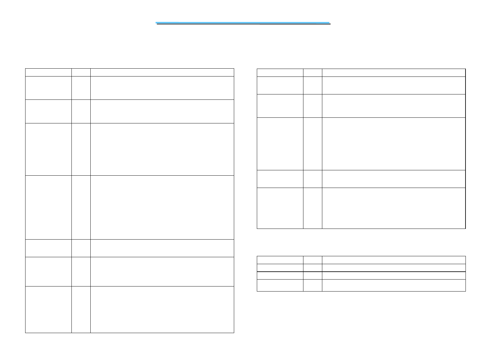
128
8170 N/B MAINTENANCE
5.3 Intel 82801BA(I/O Controller HUB )
Processor Interface Signals
Name Type Description
A20M#
O
Mask A20: A20M# goes active based on setting the appropriate bit in
the Port 92h register, or based on the A20GATE signal.
Speed Strap: During the reset sequence, ICH2 drives A20M# high if
the corresponding bit is set in the FREQ_STRP register.
CPUSLP#
O
Processor Sleep: This signal puts the processor into a state that saves
substantial power compared to Stop-Grant state. However, during that
time, no snoops occur. The ICH2 can optionally assert the CPUSLP#
signal when going to the S1 state.
FERR#
I
Numeric Coprocessor Error: This signal is tied to the coprocessor
error signal on the processor. FERR# is only used if the ICH2
coprocessor error reporting function is enabled in the General Control
Register (Device 31:Function 0, Offset D0, bit 13). If FERR# is
asserted, the ICH2 generates an internal IRQ13 to its interrupt
controller unit. It is also used to gate the IGNNE# signal to ensure
that IGNNE# is not asserted to the processor unless FERR# is active.
FERR# requires an external weak pull-up to ensure a high level when
the coprocessor error function is disabled.
IGNNE#
O Ignore Numeric Error: This signal is connected to the ignore error
pin on the processor. IGNNE# is only used if the ICH2 coprocessor
error reporting function is enabled in the General Control Register
(Device 31:Function 0, Offset D0, bit 13). If FERR# is active,
indicating a coprocessor error, a write to the Coprocessor Error
Register (F0h) causes the IGNNE# to be asserted. IGNNE# remains
asserted until FERR# is negated. If FERR# is not asserted when the
Coprocessor Error Register is written, the IGNNE# signal is not
asserted.
Speed Strap: During the reset sequence, ICH2 drives IGNNE# high
if the corresponding bit is set in the FREQ_STRP register.
INIT#
O Initialization: INIT# is asserted by the ICH2 for 16 PCI clocks to
reset the processor. ICH2 can be configured to support processor
BIST. In that case, INIT# will be active when PCIRST# is active.
INTR
O Processor Interrupt: INTR is asserted by the ICH2 to signal the
processor that an interrupt request is pending and needs to be
serviced. It is an asynchronous output and normally driven low.
Speed Strap: During the reset sequence, ICH2 drives INTR high if
the corresponding bit is set in the FREQ_STRP register.
NMI
O Non-Maskable Interrupt: NMI is used to force a non-maskable
interrupt to the processor. The ICH2 can generate an NMI when
either SERR# or IOCHK# is asserted. The processor detects an NMI
when it detects a rising edge on NMI. NMI is reset by setting the
corresponding NMI source enable/disable bit in the NMI Status and
Control Register.
Speed Strap: During the reset sequence, ICH2 drives NMI high if the
corresponding bit is set in the FREQ_STRP register.
Name Type Description
SMI# O System Management Interrupt: SMI# is an active low output
synchronous to PCICLK. It is asserted by the ICH2 in response to one
of many enabled hardware or software events.
STPCLK# O Stop Clock Request: STPCLK# is an active low output synchronous
to PCICLK. It is asserted by the ICH2 in response to one of many
hardware or software events. When the processor samples STPCLK#
asserted, it responds by stopping its internal clock.
RCIN#
I Keyboard Controller Reset Processor: The keyboard controller can
generate INIT# to the processor. This saves the external OR gate with
the ICH2’s other sources of INIT#. When the ICH2 detects the
assertion of this signal, INIT# isgenerated for 16 PCI clocks..
Note:
82801BA ICH2: The 82801BA ignores RCIN# assertion during
transitions to the S3, S4 and S5 states. 82801BAM ICH2-M: The
82801BAM ignores RCIN# assertion during transitions
to the S1, S3, S4 and S5 states.
A20GATE
I A20 Gate: This signal is from the keyboard controller. It acts as an
alternative method to force the A20M# signal active. A20GATE
saves the external OR gate needed with various other PCIsets.
CPUPWRGD
OD CPU Power Good (82801BAM ICH2-M): This signal should be
connected to the processor’s PWRGOOD input. For Intel®
SpeedStep™ technology support, this signal is kept high during a
Intel® SpeedStep™ technology state transition to prevent loss of
processor context. This is an open-drain output signal (external
pull-up resistor required) that represents a logical AND of the
ICH2-M’s PWROK and VGATE / VRMPWRGD signals.
SM Bus Interface Signals
Name Type Description
SMBDATA I/OD SMBus Data: External pull-up is required.
SMBCLK I/OD SMBus Clock: External pull-up is required.
SMBALERT#/
GPIO[11] I SMBus Alert: This signal is used to wake the system or generate an
SMI#. If not used for SMBALERT#, it can be used as a GPI.
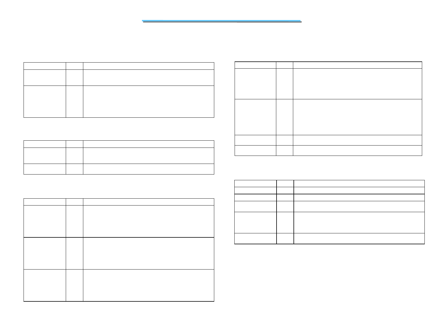
129
8170 N/B MAINTENANCE
5.3 Intel 82801BA(I/O Controller HUB )
System Management Interface Signals
Name Type Description
INTRUDER#
I Intruder Detect: This signal can be set to disable system if box
detected open. This signal’s status is readable, so it can be used like a
GPI if the Intruder Detection is not needed.
SMLINK[1:0]
I/OD System Management Link: These signals are an SMBus link to an
optional external system management ASIC or LAN controller.
External pull-ups are required.
Note:
that SMLINK[0] corresponds to an SMBus Clock signal and
SMLINK[1] corresponds to an SMBus Data signal.
Real Time Clock Interface
Name Type Description
RTCX1
Special
Crystal Input 1: This signal is connected to the 32.768 KHz crystal.
If no external crystal is used, then RTCX1 can be driven with the
desired clock rate.
RTCX2
Special
Crystal Input 2: This signal is connected to the 32.768 KHz crystal.
If no external crystal is used, then RTCX2 should be left floating.
Other Clocks
Name Type Description
CLK14
I Oscillator Clock: CLK14 is used for 8254 timers and runs at
14.31818 MHz.
82801BA ICH2: This clock is permitted to stop during S3 (or lower)
states.
82801BAM ICH2-M: This clock is permitted to stop during S1 (or
lower) states.
CLK48
I 48 MHz Clock: CLK48 is used to for the USB controller and runs at
48 MHz.
82801BA ICH2: This clock is permitted to stop during S3 (or lower)
states.
82801BAM ICH2-M: This clock is permitted to stop during S1 (or
lower) states.
CLK66
I 66 MHz Clock: CLK66 is used to for the hub interface and runs at 66
MHz.
82801BA ICH2: This clock is permitted to stop during S3 (or lower)
states.
82801BAM ICH2-M: This clock is permitted to stop during S1 (or
lower) states.
Miscellaneous Signals
Name Type Description
SPKR
O Speaker: The SPKR signal is the output of counter 2 and is internally
"ANDed" with Port 61h bit 1 to provide Speaker Data Enable. This
signal drives an external speaker driver device, which in turn drives
the system speaker. Upon PCIRST#, its output state is 1.
Note:
SPKR is sampled at the rising edge of PWROK as a functional strap.
RTCRST#
I RTC Reset: When asserted, this signal resets register bits in the RTC
well and sets the RTC_PWR_STS bit (bit 2 in GEN_PMCON3
register). Note:
Clearing CMOS in an ICH2-based platform can be done by using a
jumper on RTCRST# or GPI, or using SAFEMODE strap.
Implementations should not attempt to clear CMOS by using a
jumper to pull VccRTC low.
TP0
(ICH2 0nly) I Test Point (82801BA ICH2): This signal must have an external
pull-up to VccSus3_3.
FS0
I Functional Strap: This signal is reserved for future use. There is an
internal pullup resistor on this signal.
AC’97 Link Signals
Name Type Description
AC_RST# O AC97 Reset: Master H/W reset to external Codec(s)
AC_SYNC O AC97 Sync: 48 KHz fixed rate sample sync to the Codec(s)
AC_BIT_CLK I AC97 Bit Clock: 12.288 MHz serial data clock generated by the
external Codec(s). See Note.
AC_SDOUT
O AC97 Serial Data Out: Serial TDM data output to the Codec(s)
Note:
AC_SDOUT is sampled at the rising edge of PWROK as a functional
strap..
AC_SDIN[1:0] I AC97 Serial Data In 0: Serial TDM data inputs from the Codecs.
See Note.
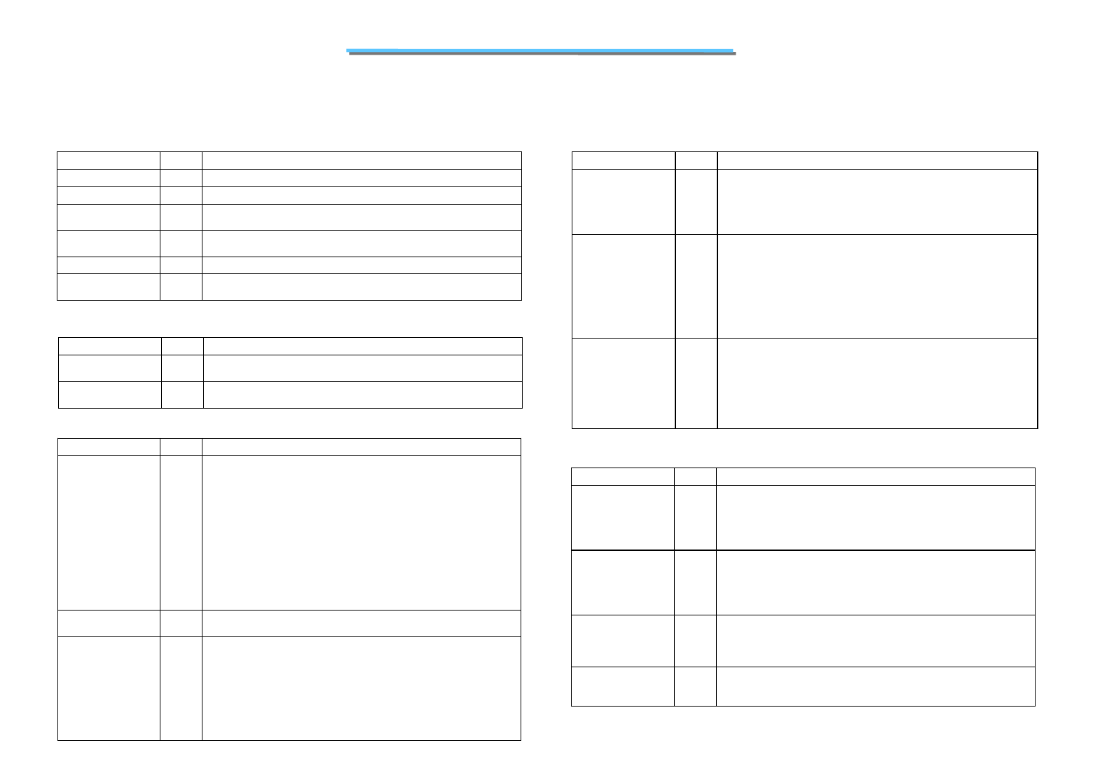
130
8170 N/B MAINTENANCE
5.4 PCI4410(PCMCIA/1394 LINK Controller )
Power-Supply Terminals
Name Type Description
GND Device ground terminals
VCC Power-supply terminal for core logic (3.3 V)
VCCB Clamp voltage for PC Card interface. Matches card signaling
environment, 5 V or 3.3 V.
VCCI
Clamp voltage for miscellaneous I/O signals (MFUNC, GRST#, and
SUSPEND#)
VCCL Clamp voltage for 1394 link function
VCCP Clamp voltage for PCI interface, ZV interface, SPKROUT, INTA#,
INTB# LED_SKT,VCCD0#, VCCD1#, VPPD0, VPPD1
PC Card Power-Switch Terminals
Name Type Description
VCCD0#
VCCD1# O
Logic controls to the TPS2211 PC Card power-switch interface to
control AVCC
VPPD0
VPPD1 O
Logic controls to the TPS2211 PC Card power-switch interface to
control AVPP
PCI System Terminals
Name Type Description
GRST#
I
Global reset. When global reset is asserted, GRST# causes the
PCI4410A device to place all output buffers in a high-impedance
state and reset all internal registers. When GRST# is asserted, the
device is completely in its default state. For systems that require
wake-up from D3, GRST# normally is asserted only during initial
boot. PRST# should be asserted following initial boot so that PME
context is retained when transitioning from D3 to D0. For systems
that do not require wake-up from D3, GRST# should be tied to PRST.
When the SUSPEND mode is enabled, the device is protected from
GRST#, and the internal registers are preserved. All outputs are
placed in a high-impedance state, but the contents of the registers are
preserved.
PCLK
I PCI bus clock. PCLK provides timing for all transactions on the PCI
bus. All PCI signals are sampled at the rising edge of PCLK.
PRST#
I
PCI bus reset. When the PCI bus reset is asserted, PRST# causes the
PCI4410A device to place all output buffers in a high-impedance
state and reset internal registers. When PRST is asserted, the device is
completely nonfunctional. After PRST# is deserted, the PCI4410A
device is in a default state. When SUSPEND# and PRST# are
asserted, the device is protected from PRST# clearing the internal
registers.All outputs are placed in a high-impedance state, but the
contents of the registers are preserved.
PCI Address and Data Terminals
Name Type Description
AD[0:31[ I/O
PCI address/data bus. These signals make up the multiplexed PCI
address and data bus on the primary interface. During the address
phase of a primary bus PCI cycle, AD31–AD0 contain a 32-bit
address or other destination information. During the data phase,
AD31–AD0 contain data.
C/BE[0:3]# I/O
PCI bus commands and byte enables. These signals are multiplexed
on the same PCI terminals. During the address phase of a primary bus
PCI cycle, C/BE3#–C/BE0# define the bus command. During the data
phase, this 4-bit bus is used as byte enables. The byte enables
determine which byte paths of the full 32-bit data bus carry
meaningful data. C/BE0# applies to byte 0 (AD7–AD0), C/BE1#
applies to byte 1 (AD15–AD8), C/BE2# applies to byte 2
(AD23–AD16), and C/BE3# applies to byte 3 (AD31–AD24).
PAR I/O PCI bus parity. In all PCI bus read and write cycles, the PCI4410A
device calculates even parity across the AD31–AD0 and
C/BE3#–C/BE0# buses. As an initiator during PCI cycles, the
PCI4410A device outputs this parity indicator with a one-PCLK
delay. As a target during PCI cycles, the calculated parity is compared
to the initiator’s parity indicator. A compare error results in the
assertion of a parity error (PERR#).
PCI Interface Control Terminals
Name Type Description
DECSEL# I/O
PCI device select. The PCI4410A device asserts DEVSEL# to claim a
PCI cycle as the target device. As a PCI initiator on the bus, the
PCI4410A device monitors DEVSEL# until a target responds. If no
target responds before timeout occurs, the PCI4410A device
terminates the cycle with an initiator abort.
FRAME# I/O
PCI cycle frame. FRAME# is driven by the initiator of a bus cycle.
FRAME# is asserted to indicate that a bus transaction is beginning,
and data transfers continue while this signal is asserted. When
FRAME# is deasserted, the PCI bus transaction is in the final data
phase.
GNT# I PCI bus grant. GNT# is driven by the PCI bus arbiter to grant the
PCI4410A device access to the PCI bus after the current data
transaction has completed. GNT# may or may not follow a PCI bus
request, depending on the PCI bus parking algorithm.
IDSEL# I Initialization device select. IDSEL# selects the PCI4410A device
during configuration space accesses. IDSEL# can be connected to one
of the upper 24 PCI address lines on the PCI bus.
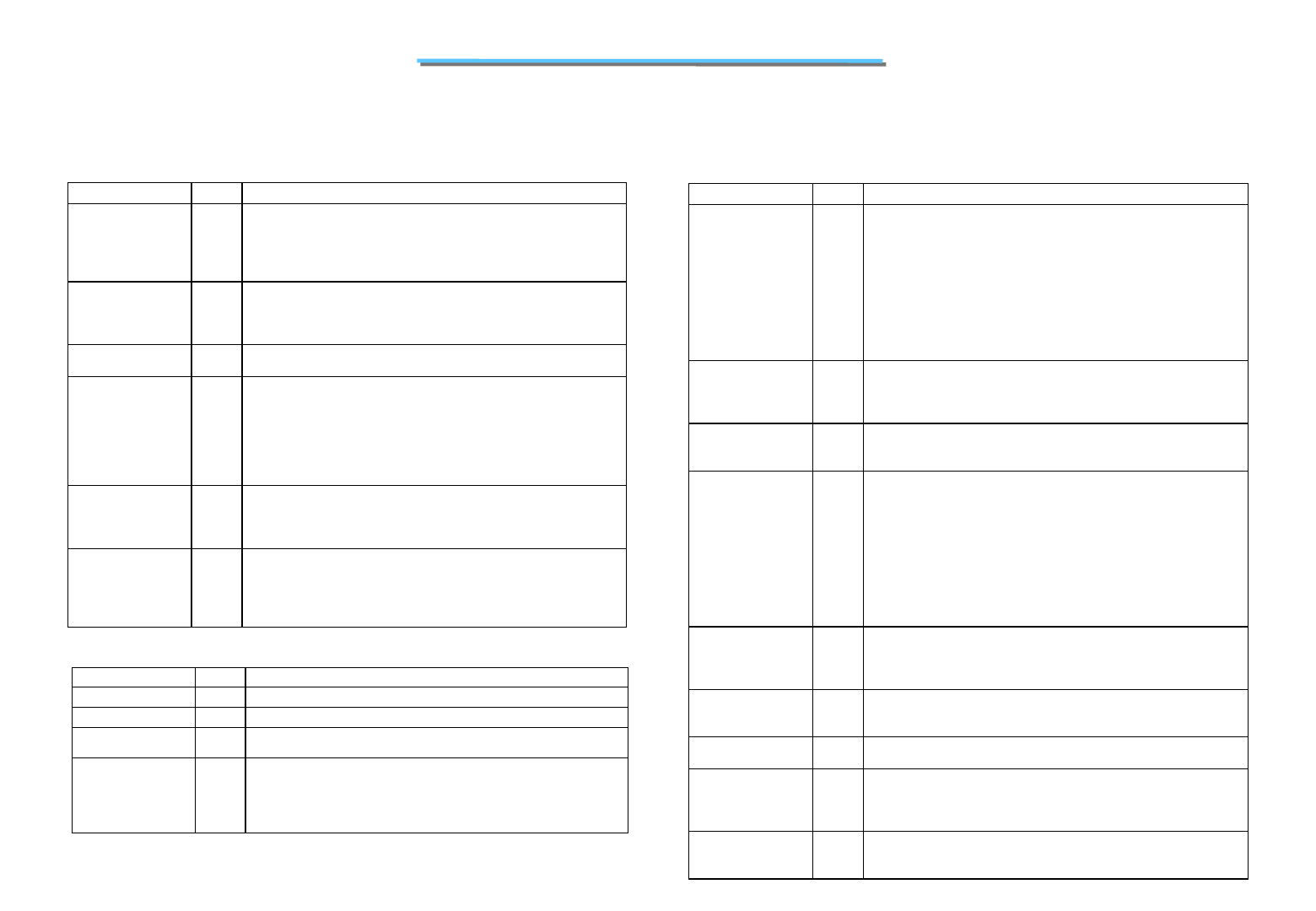
131
8170 N/B MAINTENANCE
5.4 PCI4410(PCMCIA/1394 LINK Controller )
PCI Interface Control Terminals
Name Type Description
IRDY# I/O PCI initiator ready. IRDY# indicates the PCI bus initiator’s ability to
complete the current data phase of the transaction. A data phase is
completed on a rising edge of PCLK, when both IRDY# and TRDY#
are asserted. Until IRDY# and TRDY# are both sampled asserted,
wait states are inserted.
PERR# I/O PCI parity error indicator. PERR# is driven by a PCI device to
indicate that calculated parity does not match PAR when PERR# is
enabled through bit 6 (PERR_EN) of the command register (PCI
offset 04h, see Section 4.4).
REQ# O PCI bus request. REQ# is asserted by the PCI4410A device to request
access to the PCI bus as an initiator.
SERR# O PCI system error. SERR# is an output that is pulsed from the
PCI4410A device when enabled through bit 8 (SERR_EN) of the
command register (PCI offset 04h, see Section 4.4) indicating a
system error has occurred. The PCI4410A device need not be the
target of the PCI cycle to assert this signal. When SERR# is enabled
in the command register, this signal also pulses, indicating that an
address parity error has occurred on a CardBus interface.
STOP# I/O PCI cycle stop signal. STOP# is driven by a PCI target to request the
initiator to stop the current PCI bus transaction. STOP# is used for
target disconnects and is commonly asserted by target devices that do
not support burst data transfers.
TRDY# I/O PCI target ready. TRDY# indicates the primary bus target’s ability to
complete the current data phase of the transaction. A data phase is
completed on a rising edge of PCLK, when both IRDY# and TRDY#
are asserted. Until both IRDY# and TRDY# are asserted, wait states
are inserted.
Multifunction and Miscellaneous Terminals
Name Type Description
INTA# O Parallel PCI interrupt. INTA#
INTB# O Parallel PCI interrupt. INTB#
LED_SKT O PC Card socket activity LED indicator. LED_SKT provides an output
indicating PC Card socket activity.
MFUNC0 I/O Multifunction terminal 0. MFUNC0 can be configured as parallel PCI
interrupt INTA#, GPI0, GPO0, socket activity LED output, ZV
switching outputs, CardBus audio PWM, GPE#, or a parallel IRQ.
See Section 4.32, Multifunction Routing Register, for configuration
details.
Name Type Description
MFUNC1 I/O Multifunction terminal 1. MFUNC1 can be configured as GPI1,
GPO1, socket activity LED output, ZV switching outputs, CardBus
audio PWM, GPE#, or a parallel IRQ. See Section 4.32,
Multifunction Routing Register, for configuration details.
Serial data (SDA). When VCCD0# and VCCD1# are high after a PCI
reset, the MFUNC1 terminal provides the SDA signaling for the serial
bus interface. The two-terminal serial interface loads the subsystem
identification and other register defaults from an EEPROM after a
PCI reset. See Section 3.6.1, Serial Bus Interface Implementation, for
details on other serial bus applications.
MFUNC2 I/O Multifunction terminal 2. MFUNC2 can be configured as PC/PCI
DMA request, GPI2, GPO2, ZV switching outputs, CardBus audio
PWM, GPE#, RI_OUT#, or a parallel IRQ. See Section 4.32,
Multifunction Routing Register, for configuration details.
MFUNC3 I/O Multifunction terminal 3. MFUNC3 can be configured as a parallel
IRQ or the serialized interrupt signal IRQSER. See Section 4.32,
Multifunction Routing Register, for configuration details.
MFUNC4 I/O Multifunction terminal 4. MFUNC4 can be configured as PCI
LOCK#, GPI3, GPO3, socket activity LED output, ZV switching
outputs, CardBus audio PWM, GPE#, RI_OUT#, or a parallel IRQ.
See Section 4.32, Multifunction Routing Register, for configuration
details. Serial clock (SCL). When VCCD0# and VCCD1# are high
after a PCI reset, the MFUNC4 terminal provides the SCL signaling
for the serial bus interface. The two-terminal serial interface loads the
subsystem identification and other register defaults from an EEPROM
after a PCI reset. See Section 3.6.1, Serial Bus Interface
Implementation, for details on other serial bus applications.
MFUNC5 I/O Multifunction terminal 5. MFUNC5 can be configured as PC/PCI
DMA grant, GPI4, GPO4, socket activity LED output, ZV switching
outputs, CardBus audio PWM, GPE#, or a parallel IRQ. See Section
4.32, Multifunction Routing Register, for configuration details.
MFUNC6 I/O Multifunction terminal 6. MFUNC6 can be configured as a PCI
CLKRUN# or a parallel IRQ. See Section 4.32, Multifunction
Routing Register, for configuration details.
RI_OUT#/PME#
O Ring indicate out and power-management event output. Terminal
provides an output for ring-indicate or PME# signals.
SPKROUT O Speaker output. SPKROUT is the output to the host system that can
carry SPKR# or CAUDIO through the PCI4410A device from the PC
Card interface. SPKROUT is driven as the exclusive-OR combination
of card SPKR#//CAUDIO inputs.
SUSPEND# I Suspend. SUSPEND# protects the internal registers from clearing
when the GRST or PRST signal is asserted. See Section 3.8.4,
Suspend Mode, for details.
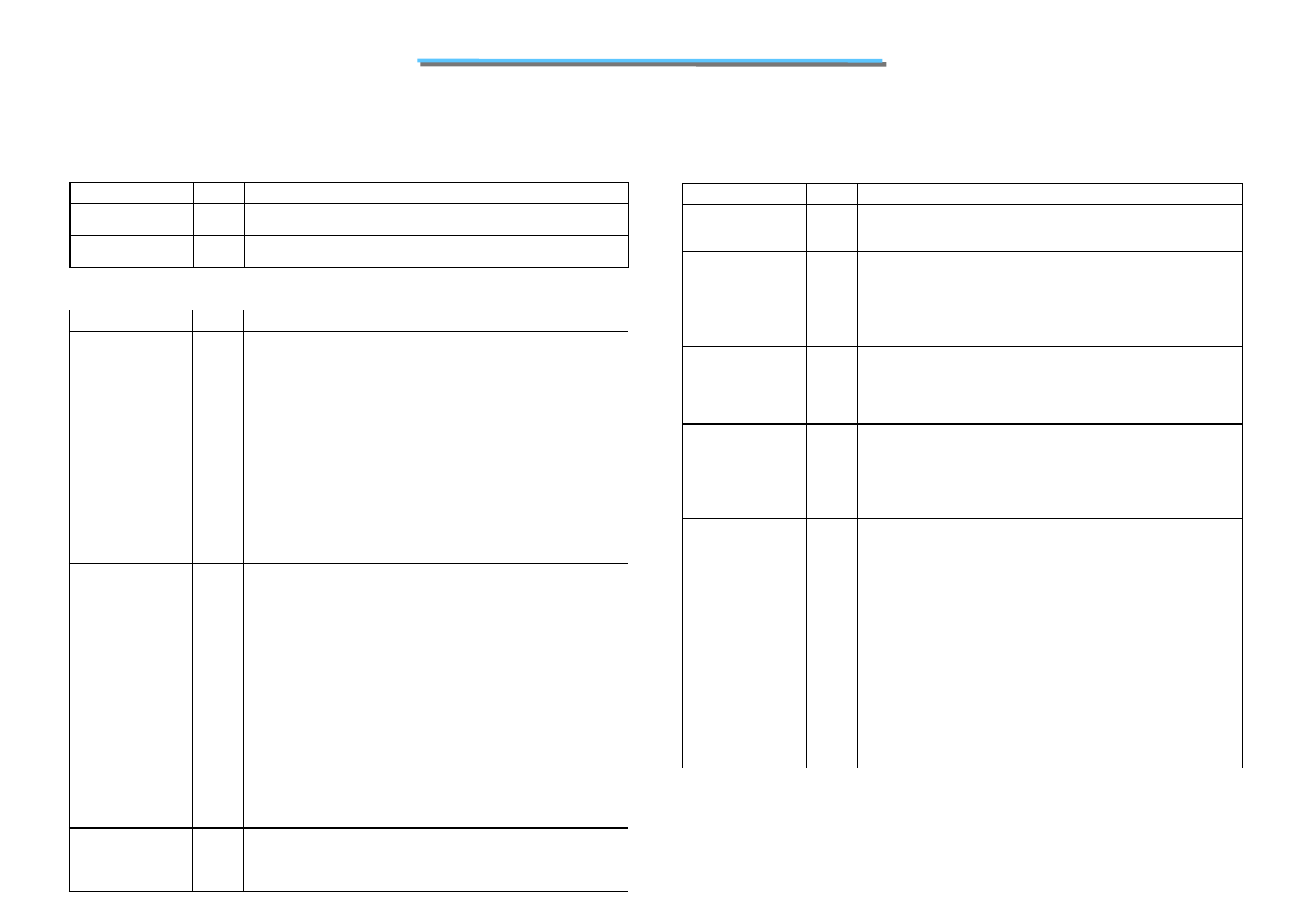
132
8170 N/B MAINTENANCE
5.4 PCI4410(PCMCIA/1394 LINK Controller )
16-Bit PC Card Address and Data Terminals
Name Type Description
ADDR[0:25] O PC Card address. 16-bit PC Card address lines. ADDR25 is the most
significant bit
DATA[0:15] I/O
PC Card data. 16-bit PC Card data lines. DATA15 is the most
significant bit.
16-Bit PC Card Interface Control Terminals
Name Type Description
BVD1
(STSCHG#/RI#)
I
Battery voltage detect 1. BVD1 is generated by 16-bit memory PC
Cards that include batteries. BVD1 is used with BVD2 as an
indication of the condition of the batteries on a memory PC Card.
Both BVD1 and BVD2 are high when the battery is good. When
BVD2 is low and BVD1 is high, the battery is weak
and should be replaced. When BVD1 is low, the battery is no longer
serviceable and the data in the memory PC Card is lost. See Section
5.6, ExCA Card Status-Change-Interrupt Configuration Register, for
enable bits. See Section 5.5, ExCA Card Status-Change Register, and
Section 5.2,ExCA Interface Status Register, for the status bits for this
signal. Status change. STSCHG# is used to alert the system to a
change in the READY, write protect, or battery voltage dead
condition of a 16-bit I/O PC Card. Ring indicate. R# is used by 16-
b
it
modem cards to indicate a ring detection.
BVD2
(SPKR#) I Battery voltage detect 2. BVD2 is generated by 16-bit memory PC
Cards that include batteries. BVD2is used with BVD1 as an
indication of the condition of the batteries on a memory PC Card.
Both BVD1and BVD2 are high when the battery is good. When
BVD2 is low and BVD1 is high, the battery is weak and should be
replaced. When BVD1 is low, the battery is no longer serviceable and
the data in the memory PC Card is lost. See Section 5.6, ExCA Card
Status-Change-Interrupt Configuration Register, for enable bits. See
Section 5.5, ExCA Card Status-Change Register, and Section 5.2,
ExCA Interface Status Register, for the status bits for this signal.
Speaker. SPKR# is an optional binary audio signal available only
when the card and socket have been configured for the 16-bit I/O
interface. The audio signals from cards A and B are combined by the
PCI4410A device and are output on SPKROUT.DMA request. BVD2
can be used as the DMA request signal during DMA operations to a
16-bit PC Card that supports DMA. The PC Card asserts BVD2 to
indicate a request for a DMA operation.
CD1#
CD2#
I Card detect 1 and Card detect 2. CD1# and CD2# are connected
internally to ground on the PC Card. When a PC Card is inserted into
a socket, CD1# and CD2# are pulled low. For signal status, see
Section 5.2, ExCA Interface Status Register.
Name Type Description
CE1#
CE2# O Card enable 1 and card enable 2. CE1# and CE2# enable even- and
odd-numbered address bytes. CE1#enables even-numbered address
bytes, and CE2# enables odd-numbered address bytes.
INPACK# I Input acknowledge. INPACK# is asserted by the PC Card when it
can respond to an I/O read cycle at the current address.DMA request.
INPACK# can be used as the DMA request signal during DMA
operations from a 16-bit PC Card that supports DMA. If it is used as a
strobe, the PC Card asserts this signal to indicate a request for a DMA
operation.
IORD# O I/O read. IORD# is asserted by the PCI4410A device to enable 16-
b
it
I/O PC Card data output during host I/O read cycles. DMA write.
IORD# is used as the DMA write strobe during DMA operations from
a 16-bit PC Card that supports DMA. The PCI4410A device asserts
IORD# during DMA transfers from the PC Card to host memory.
IOWR# O I/O write. IOWR# is driven low by the PCI4410A device to strobe
write data into 16-bit I/O PC Cards during host I/O write cycles.
DMA read. IOWR# is used as the DMA write strobe during DMA
operations from a 16-bit PC Card that supports DMA. The PCI4410A
device asserts IOWR during transfers from host memory to the PC
Card.
OE# O Output enable. OE# is driven low by the PCI4410A device to enable
16-bit memory PC Card data output during host memory read cycles.
DMA terminal count. OE# is used as terminal count (TC) during
DMA operations to a 16-bit PC Card that supports DMA. The
PCI4410A device asserts OE# to indicate TC for a DMA write
operation.
READ
IREQ# I Ready. The ready function is provided by READY when the 16-bit
PC Card and the host socket are configured for the memory-only
interface. READY is driven low by the 16-bit memory PC Cards to
indicatethat the memory card circuits are busy processing a previous
write command. READY is driven high when the 16-bit memory PC
Card is ready to accept a new data-transfer command. Interrupt
request. IREQ# is asserted by a 16-bit I/O PC Card to indicate to the
host that a device on the 16-bit I /O PC Card requires service by the
host software. IREQ# is high (deasserted) when no interrupt is
requested.
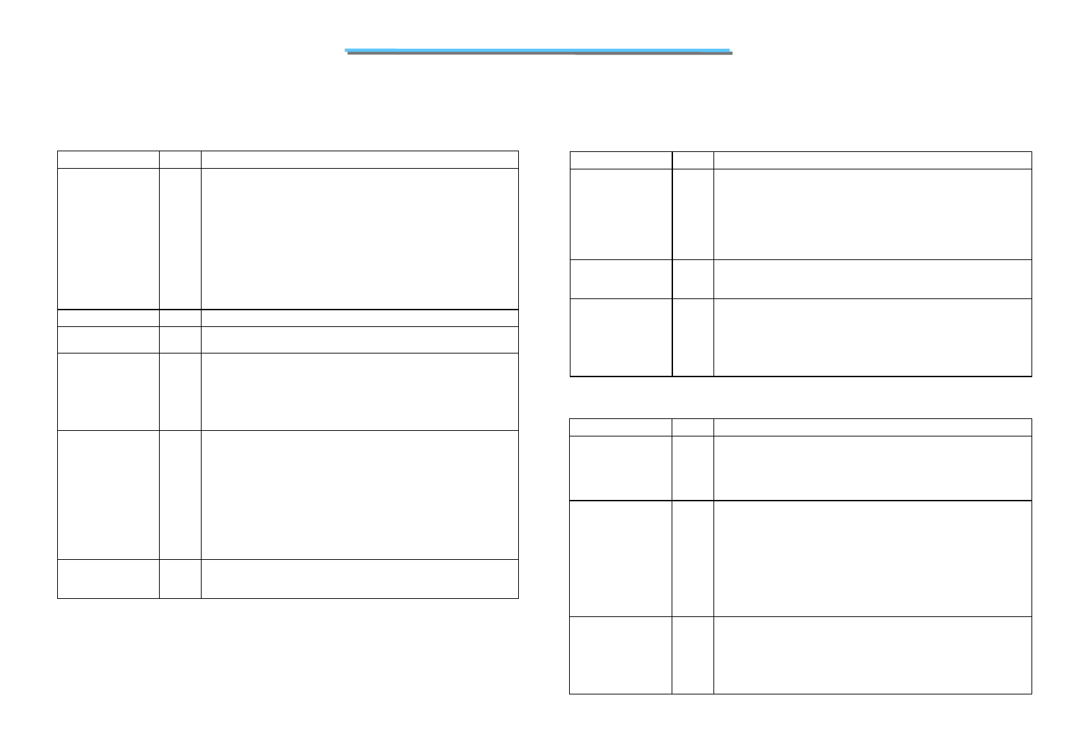
133
8170 N/B MAINTENANCE
5.4 PCI4410(PCMCIA/1394 LINK Controller )
16-Bit PC Card Interface Control Terminals
Name Type Description
REG#
O Attribute memory select. REG# remains high for all common
memory accesses. When REG# is asserted, access is limited to
attribute memory (OE# or WE# active) and to the I/O space (IORD#
or IOWR# active). Attribute memory is a separately accessed section
of card memory and generally is used to record card capacity and
other configuration and attribute information. DMA acknowledge.
REG is used as a DMA acknowledge (DACK#) during DMA
operations to a 16-bit PC Card that supports DMA. The PCI4410A
device asserts REG# to indicate a DMA operation. REG# is used in
conjunction with the DMA read (IOWR#) or DMA write (IORD#)
strobes to transfer data.
RESET O PC Card reset. RESET forces a hard reset to a 16-bit PC Card.
WA IT # I Bus cycle wait. WAIT# is driven by a 16-bit PC Card to extend the
completion of the memory or I/O cycle in progress.
WE# O Write enable. WE# is used to strobe memory write data into 16-bit
memory PC Cards. WE# also is used for memory PC Cards that
employ programmable memory technologies. DMA terminal count.
WE# is used as TC during DMA operations to a 16-bit PC Card that
supports DMA. The PCI4410A device asserts WE to indicate TC for
a DMA read operation.
WP
IOIS16# I Write protect. WP applies to 16-bit memory PC Cards. WP reflects
the status of the write-protect switch on 16-
b
it memory PC Cards. For
16-bit I/O PC cards, WP is used for the 16-bit port (IOIS16#)
function. I/O is 16 bits. IOIS16# applies to 16-bit I/O PC Cards.
IOIS16# is asserted by the 16-bit PC Card when the address on the
bus corresponds to an address to which the 16-bit PC Card responds,
and the I/O port that is addressed is capable of 16-bit accesses.
DMA request. WP can be used as the DMA request signal during
DMA operations to a 16-bit PC Card that supports DMA. If used, the
PC Card asserts WP to indicate a request for a DMA operation.
VS1#
VS2# I/O Voltage sense 1 and voltage sense 2. VS1 and VS2, when used in
conjunction with each other, determine the operating voltage of the
PC Card.
CardBus PC Card Interface System Terminals
Name Type Description
CCLK O
CardBus clock. CCLK provides synchronous timing for all
transactions on the CardBus interface. All signals except CRST#,
CCLKRUN#, CINT#, CSTSCHG, CAUDIO, CCD2#, CCD1#,
CVS2, and CVS1 are sampled on the rising edge of CCLK, and all
timing parameters are defined with the rising edge of this signal.
CCLK operates at the PCI bus clock frequency, but it can be stopped
in the low state or slowed down for power savings.
CCLKRUN# I/O
CardBus clock run. CCLKRUN# is used by a CardBus PC Card to
request an increase in the CCLK frequency, and by the PCI4410A
device to indicate that the CCLK frequency is going to be decreased.
CRST# O
CardBus reset. CRST# brings CardBus PC Card-specific registers,
sequencers, and signals to a known state. When CRST# is asserted,
all CardBus PC Card signals are placed in a high-impedance state,
and the PCI4410A device drives these signals to a valid logic level.
Assertion can be asynchronous to CCLK, but deassertion must be
synchronous to CCLK.
CardBus PC Card Address and Data Terminals
Name Type Description
CAD[0:31] I/O
CardBus address and data. These signals make up the multiplexed
CardBus address and data bus on the CardBus interface. During the
address phase of a CardBus cycle, CAD31–CAD0 contain a 32-bit
address. During the data phase of a CardBus cycle, CAD31–CAD0
contain data. CAD31 is the most significant bit.
CC/BE[0:3]# I/O
CardBus bus commands and byte enables. CC/BE3#–CC/BE0# are
multiplexed on the same CardBus terminals. During the address phase
of a CardBus cycle, CC/BE3#–CC/BE0# define the bus command.
During the data phase, this 4-bit bus is used as byte enables. The byte
enables determine which byte paths of the full 32-bit data bus carry
meaningful data. CC/BE0# applies to byte 0 (CAD7–CAD0),
CC/BE1# applies to byte 1 (CAD15–CAD8), CC/BE2# applies to
byte 2 (CAD23–CAD16), and CC/BE3# applies to byte 3
(CAD31–CAD24).
CPAR I/O
CardBus parity. In all CardBus read and write cycles, the PCI4410A
device calculates even parity across the CAD and CC/BE buses. As
an initiator during CardBus cycles, the PCI4410A device outputs
CPAR with a one-CCLK delay. As a target during CardBus cycles,
the calculated parity is compared to the initiator’s parity indicator; a
compare error results in a parity-error assertion.
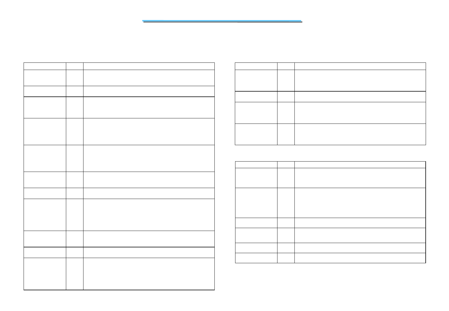
134
8170 N/B MAINTENANCE
5.4 PCI4410(PCMCIA/1394 LINK Controller )
CardBus PC Card Interface Control Terminals
Name Type Description
CAUDIO I CardBus audio. CAUDIO is a digital input signal from a PC Card to
the system speaker. The PCI4410A device supports the binary audio
mode and outputs a binary signal from the card to SPKROUT.
CBLOCK# I/O CardBus lock. CBLOCK# is used to gain exclusive access to a
target.
CCD1#
CCD2# I CardBus detect 1 and CardBus detect 2. CCD1# and CCD2# are
used in conjunction with CVS1 and CVS2 to identify card insertion
and interrogate cards to determine the operating voltage and card
type.
CDEVSEL# I/O CardBus device select. The PCI4410A device asserts CDEVSEL# to
claim a CardBus cycle as the target device. As a CardBus initiator on
the bus, the PCI4410A device monitors CDEVSEL# until a target
responds. If no target responds before timeout occurs, the PCI4410A
device terminates the cycle with an initiator abort.
CFRAME# I/O
CardBus cycle frame. CFRAME# is driven by the initiator of a
CardBus bus cycle. CFRAME# is asserted to indicate that a bus
transaction is beginning, and data transfers continue while this signal
is asserted. When CFRAME# is deasserted, the CardBus bus
transaction is in the final data phase.
CGNT# O CardBus bus grant. CGNT# is driven by the PCI4410A device to
grant a CardBus PC Card access the CardBus bus after the current
data transaction has been completed.
CINT# I CardBus interrupt. CINT# is asserted low by a CardBus PC Card to
request interrupt servicing from the host.
CIRDY# I/O CardBus initiator ready. CIRDY indicates the CardBus initiator’s
ability to complete the current data
phase of the transaction. A data phase is completed on a rising edge
of CCLK when both CIRDY and
CTRDY are asserted. Until both CIRDY and CTRDY are sampled
asserted, wait states are inserted.
CPERR# I/O CardBus parity error. CPERR# reports parity errors during CardBus
transactions, except during special cycles. It is driven low by a target
two clocks following that data when a parity error is detected.
CREQ# I CardBus request. CREQ# indicates to the arbiter that the CardBus
PC Card desires use of the CardBus bus as an initiator.
CSERR# I CardBus system error. CSERR# reports address parity errors and
other system errors that could lead to catastrophic results. CSERR# is
driven by the card synchronous to CCLK, but deasserted by a weak
pull up, and may take several CCLK periods. The PCI4410A device
can report CSERR# to the system by assertion of SERR# on the PCI
interface.
Name Type Description
CSTOP# I/O CardBus stop. CSTOP# is driven by a CardBus target to request the
initiator to stop the current CardBus transaction. CSTOP# is used for
target disconnects, and is commonly asserted by target devices
do not support burst data transfers.
CSTSCHG# I CardBus status change. CSTSCHG alerts the system to a change in
the card’s status, and is used a wake-up mechanism.
CTRDY# I/O CardBus target ready. CTRDY# indicates the CardBus target’s
ability to complete the current data phase of the transaction. A data
p
hase is completed on a rising edge of CCLK, when both CIRDY and
CTRDY# are asserted; until this time, wait states are inserted.
CVS1
CVS2 CardBus voltage sense 1 and CardBus voltage sense 2. CVS1 and
CVS2 are used in conjunction with CCD1# and CCD2# to identify
card insertion and interrogate cards to determine the operating voltage
and card type.
IEEE 1394 PHY/Link Interface Terminals
Name Type Description
PHY_CTL1
PHY_CTL0
I/O
PHY-link interface control. These bidirectional signals control
passage of information between the PHY and link. The link can drive
these terminals only after the PHY has granted permission, following
a link request (LREQ).
PHY_DATA[0:7] I/O
PHY-link interface data. These bidirectional signals pass data
between the PHY and link. These terminals are driven by the link on
transmissions and are driven by the PHY on receptions. Only
DATA1–DATA0 are valid for 100-Mbit speed. DATA4–DATA0 are
valid for 200-Mbit speed and DATA7–DATA0 are valid for 400-Mbit
speed.
PHY_CLK I
System clock. This input provides a 49.152-MHz clock signal for
data synchronization.
PHY_REQ O
Link request. This signal is driven by the link to initiate a request for
the PHY to perform some
service.
LINKON I 1394 link on. This input from the PHY indicates that the link should
turn on.
LPS O
Link power status. LPS indicates that link is powered and fully
functional.
135
8170 N/B MAINTENANCE
5.4 PCI4410(PCMCIA/1394 LINK Controller )
Zoomed-Video Interface Terminals
Name Type Description
ZV_HREF O Horizontal sync to the zoomed-video port
ZV_VSYHC O Vertical sync to the zoomed-video port
ZV_Y[0:7] O Video data to the zoomed-video port in YUV:4:2:2 format
ZV_UV[0:7] O Video data to the zoomed-video port in YUV:4:2:2 format
ZV_SCLK O Audio SCLK PCM
ZV_MCLK O Audio MCLK PCM
ZV_PCLK IO Pixel clock to the zoomed-video port
ZV_LRCLK O Audio LRCLK PCM
ZV-SDATA O Audio SDATA PCM
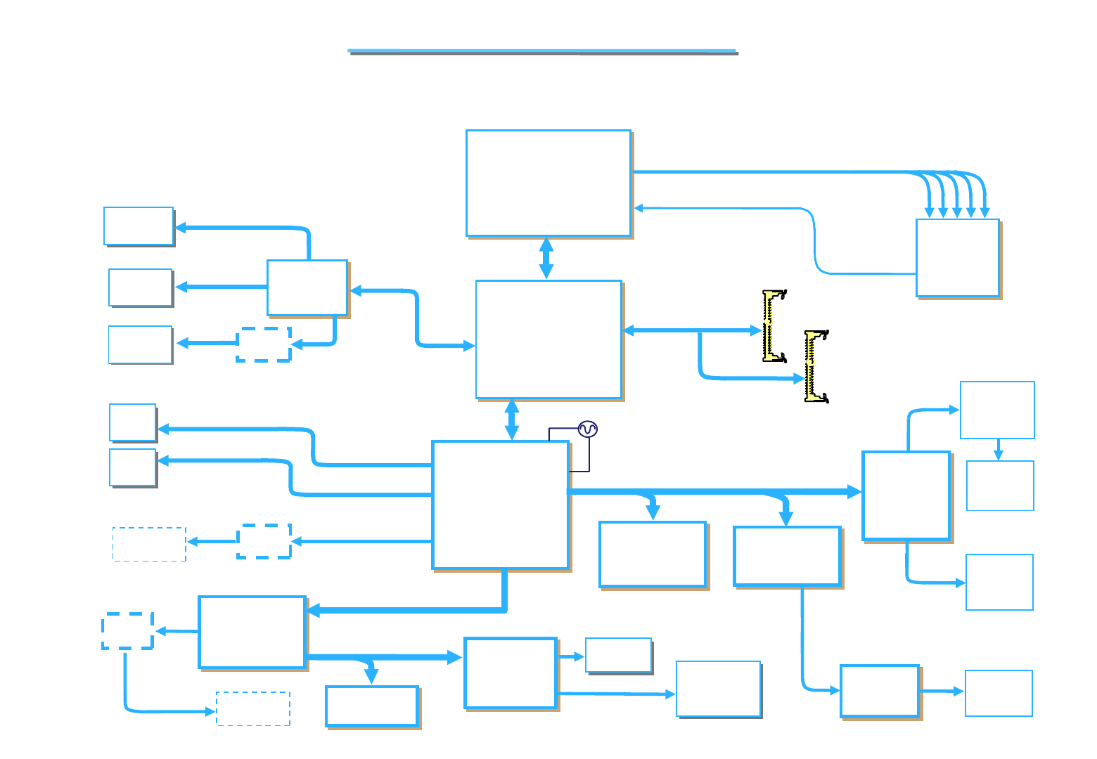
136
8170 N/B MAINTENANCE
6. System Block Diagram
U8
82801BA ICH2
360 PIN mBGA
U8
82801BA ICH2
360 PIN mBGA
PCI BUS 33M
HDD
CD-ROM
USB
X3
32.768KHZ
J503 SO-DIMM1
J505 SO-DIMM2
133M
400M
AGP4X 66M
U509
Supper I/O
PC87393
U509
Supper I/O
PC87393
LPC BUS
U516
ATI VGA U3
82845 MCH
593 PIN
mBGA
U1
Pentium 4
mFC-PGA2 478 Pin
J2
LCD Panel
J1
Monitor
ISA BUS U508
H8/3437
U508
H8/3437
U4
LANPHY
RTL8139CL
U4
LANPHY
RTL8139CL
U15
AUDIO CODEC
U15
AUDIO CODEC
U18
Amplifier
U18
Amplifier J19
Line Out
U7
PCI4410
U7
PCI4410
U14
1394
TSB41AB1
J8
Card BUS
Socket
J21
Mini
1394
J12
Internal
Keyboard
U12
Flash ROM
U12
Flash ROM
J15
Touch Pad
D/D
Board
J1
PIO Port
J5
TV OUT D/D
Board
VID[0:4]
CPU_CORE PU508
LTC1709
D/D
Board
J2,J3
USB Port
J14
IDE1
J10
IDE2

137
8170 N/B MAINTENANCE
7. Maintenance Diagnostic
7.1 Introduction
Every time the computer is turned on ,the system BIOS runs a series of internal checks on the
hardware. This power-on self test (post) allows the computer to detect problems as early as the
power-on stage. Error messages of post can alert you to the problems of your computer.
If an error is detected during these tests, you will see an error message displayed on the screen. If
the error occurs before the display, then the screen cannot display the error message. Error codes
or system beeps are used to identify a post error that occurs when the screen is not available.
The value for the diagnostic post (378H) is written at the beginning of the test. Therefore , if the
test fail, the user can determine where the problem occurs by reading the last value written to
post 378H by the PIO debug board plug at PIO port.
138
8170 N/B MAINTENANCE
7.2 Error codes :
Following is a list of error codes in sequent display on the PIO debug board.
Test 8237A page registers1Fh
Initialize monochrome adapter1Eh
Initialize color adapter1Dh
Initialize video (6845Regs)1Ch
Initialize video adapter(s)1Bh
Reset PIC’s1Ah
Check sum the ROM19h
Dispatch to RAM test18h
Sizememory17h
User register config through CMOS16h
Reset counter / Timer 115h
Search for ISA Bus VGA adapter14h
Initialize the chipset13h
Signal power on reset12h
Turn off FAST A20 for POST11h
Some type of lone reset10h
POST Routine DescriptionCode
Signon messages displayed2Fh
Search for color adapter2Eh
Search for monochrome adapter2Dh
Going to initialize video2Ch
Setup shadow2Bh
Protected mode exit successful2Ah
RAM test completed29h
Protected mode entered safely28h
RAM quick sizing27h
Initialize int vectors26h
Initialize 8237A controller25h
Test the DMA controller24h
Test battery fail & CMOS X-SUM23h
Check if CMOS RAM valid22h
Test keyboard controller21h
Test keyboard20h
POST Routine DescriptionCode
139
8170 N/B MAINTENANCE
7.2 Error codes :
Following is a list of error codes in sequent display on the PIO debug board.
Special init of COMM and LPT ports3Fh
Update NUMLOCK status3Eh
Search and init the mouse3Dh
Initialize the hardware vectors3Ch
Test for RTC ticking3Bh
Test if 18.2Hz periodic working3Ah
Setup cache controller39h
Update output port38h
Protected mode exit successful37h
RAM test complete36h
Protected mode entered safely(2)35h
Test, blank and count all RAM34h
Test keyboard command byte33h
Test keyboard Interrupt32h
Test if keyboard Present31h
Special init of keyboard ctlr30h
POST Routine DescriptionCode
Jump into bootstrap code49h
Dispatch to operate system boot48h
OEM functions before boot47h
Test for coprocessor installed46h
Update NUMLOCK status45h
OEM’s init of power management44h
Initialize option ROMs43h
Initialize the hard disk42h
Initialize the floppies41h
Configure the COMM and LPT ports40h
POST Routine DescriptionCode
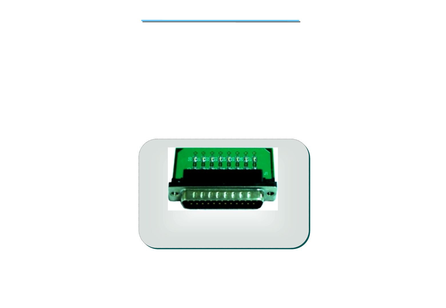
140
8170 N/B MAINTENANCE
7.3 Debug Card
7.3.1 Diagnostic Tools :
P/N:411904800001
DESCRIPTION :PWA;PWA-378PORT DEBUG BD
Note:Order it from MIC/TSSC
The 378 Port Debug Card, a kind of tool, is designed mainly for Notebook . It can be used to test the
process of BIOS POST system. It composed of eight . LED and one PIO CONNECTOR as the below
figure shows
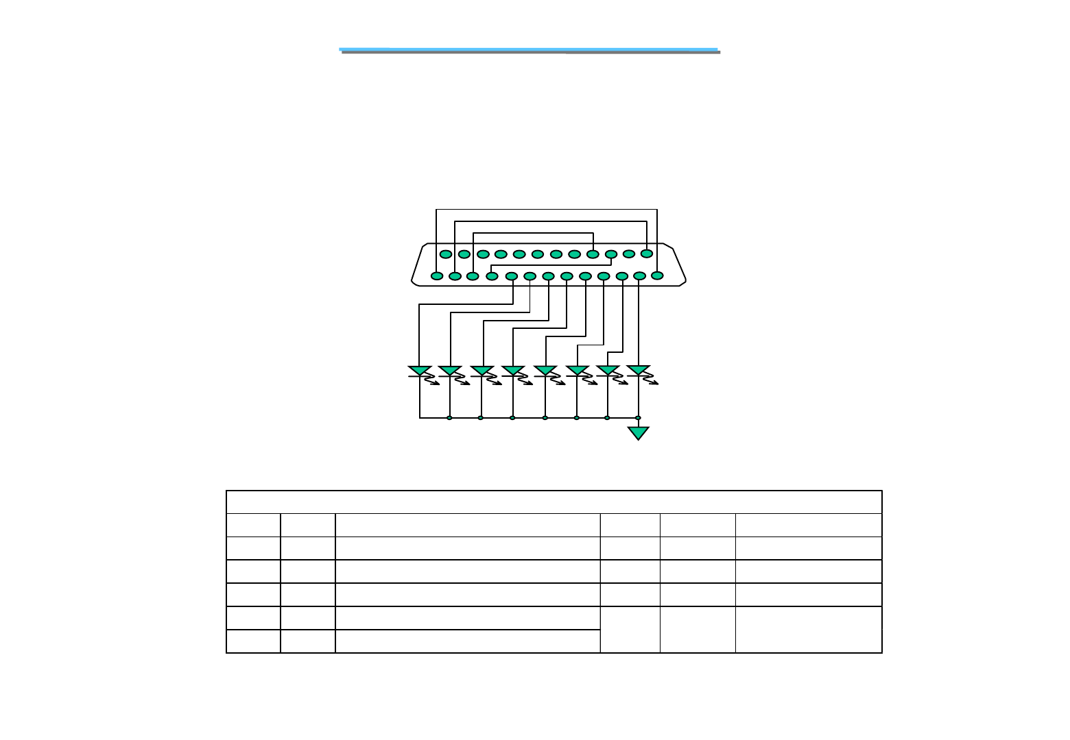
141
8170 N/B MAINTENANCE
7.3 Debug Card
7.3.2 CIRCUIT:
PIO
CONNECTOR
LED
1
13
14
25
PIN 1 STB STROBE SIGNAL PIN 14 AFD AUTO LINE FEED
PIN 2-9 D0 - D7
P
ARALLEL PORT DATA BUS D0 TO D7 PIN15 ERR ERROR AT PRINTER
PIN10 ACK ACKNOWLEDGE HANDSHANK PIN16 INIT INITIATE OUTPUT
PIN11 BUSY BUSY SIGNAL PIN17 SLIN PRINTER SELECT
PIN12 PE PAPER END
PIN13 SLCT PRINTER SELECTED
PIN DEFINITION OF PIO PORT
PIN18-25 SIGNAL
GROUND

142
8170 N/B MAINTENANCE
8.1 No Power
8.3 No Display
8.2 Battery Can not Be Charged
8.4 VGA Controller Failure LCD No Display
8.5 VGA Controller Failure External Monitor
No Display
8.6 Memory Test Error
8.7 Keyboard(K/B) and Touch Pad(T/B) Test Error
8.8 Hard Drive Test Error
8.11 PIO Port Test Error
8.12 PC-Card Failure
8.14 Audio Failure
8.15 LAN Test Error
8.10 USB Port Test Error
8.13 IEEE1394 Failure
8.Trouble Shooting
8.9 CD-ROM Drive Test Error
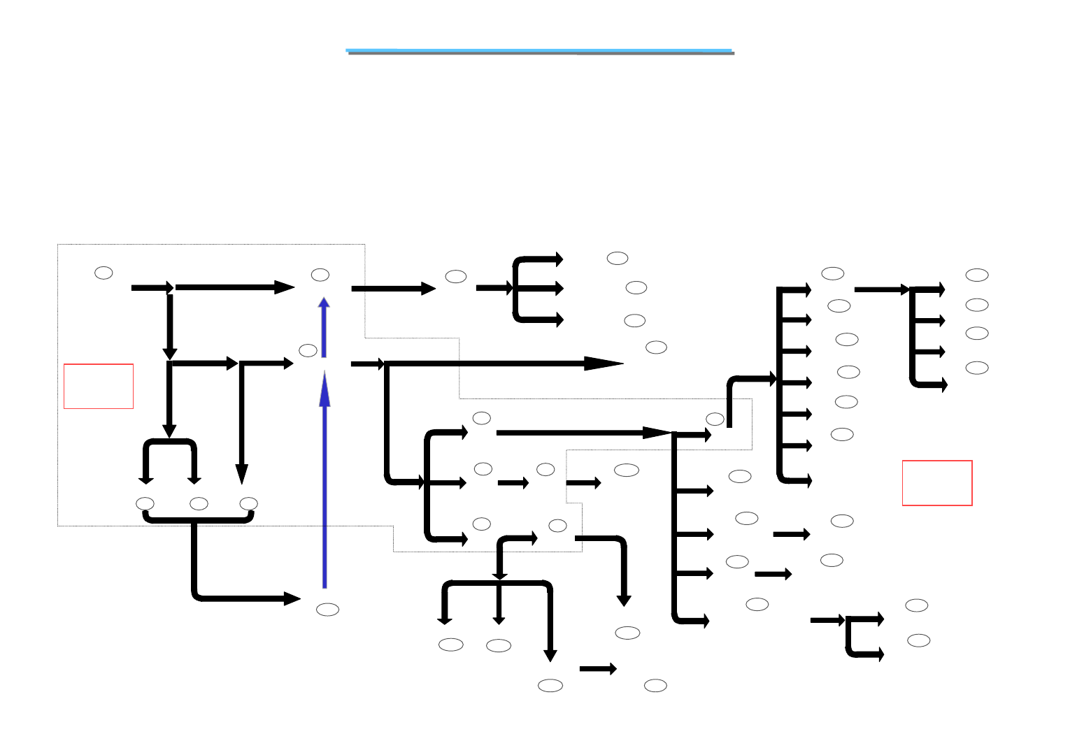
143
8170 N/B MAINTENANCE
8.1 No Power
When the power button is pressed, nothing happens, no fan activity is heard and power indicator is not light up.
Power In
J5
PF501
PL502
PL503
PD501
PQ502
PQ503
P2
ADNP ADNP_1
JL2
PR513
PR514
ADNP_2
JL3
PD4-PD6 DVMAIN
JS7 PU7 PL8 +5VA
PQ512 +5VAS
PL500 PL501PU1,
PU2,PU500-PU508 CPU_CORE
PU1 PL3 +12V
PU502
PU503 +5V
PQ2 +12VS
PU511,PU5
PU6,PL7,
PU512,PU9
PD4-PD6
DBATT
U511
JS502 AVDDAD
PU504 +5VS JS10
5V_AMP
U504
VCCA
VPPA
PU505
PU506 +3V PU501 +3VS
PU12 +1.8VS
Q514 +3VS_SPD
L12 +3V_LAN L10 AVDD_LAN
L20 1394AVDD
+3V_ICH PU514
D509 VCC_RTC
U505 VDDR_MEM2.5
L6,L7 VDD_DAC1.8
L507 VDD_PLL1.8
L4 VDD_PNLLL1.8
L514 VDD_MEMPLL1.8
L517 +3VCLKCPU
L516 +3VCLKPCI
L518 +3VCLKANA
L519 +3VCLK66
JL1 VCC3_IR
PU10
PU11
Charge
Board
P2
PD2 ALWAYS
P2 P2 P2
P2
P22
P2
P1
P1
P1
P2
P2
P21
PU13 +1.5VS
P21
P21
P21
P20
P20
L520 H8_VDD5 P19
P17
P17
P16 P16
P15
P15 P15
P13
P11
P11
P11
P11
P11
P8
P8
P8
P8
R33 AGP_VREF
P10
L506
L11 VDD_MCLK2.5
VDD_DAC2.5
P11
P11
P17
P20
PU8
+1.8V_ICH
Mother
Board
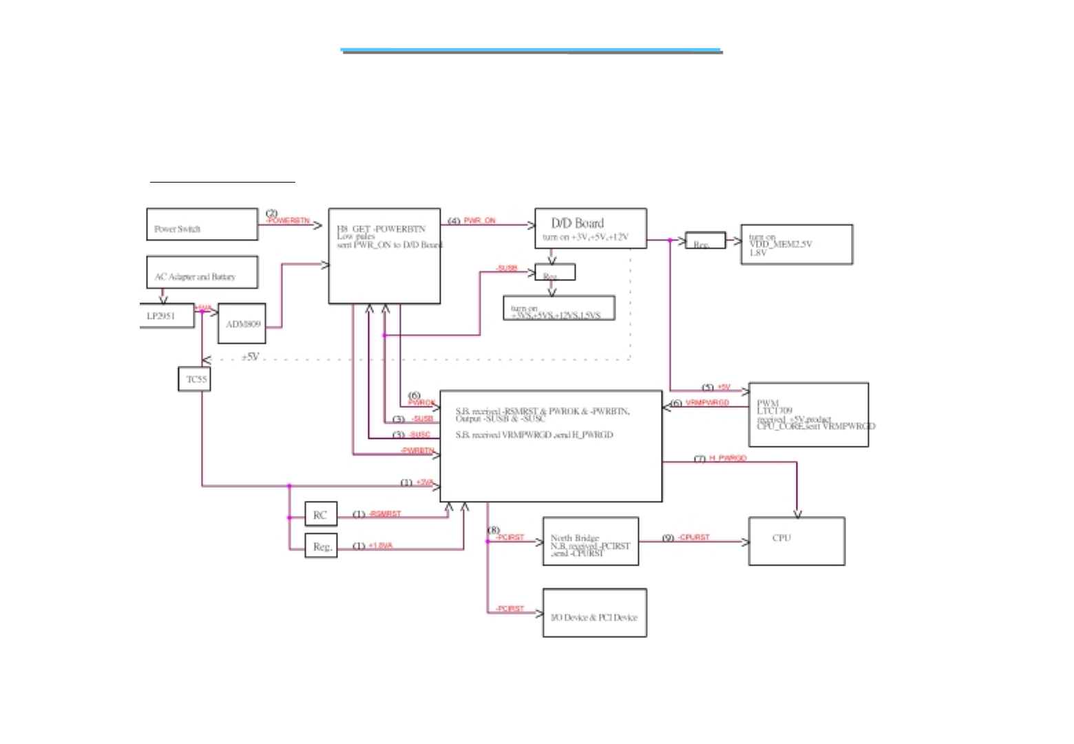
144
8170 N/B MAINTENANCE
8.1 No Power (1)
When the power button is pressed, nothing happens, no fan activity is heard and power indicator is not light up.
Power on Sequence
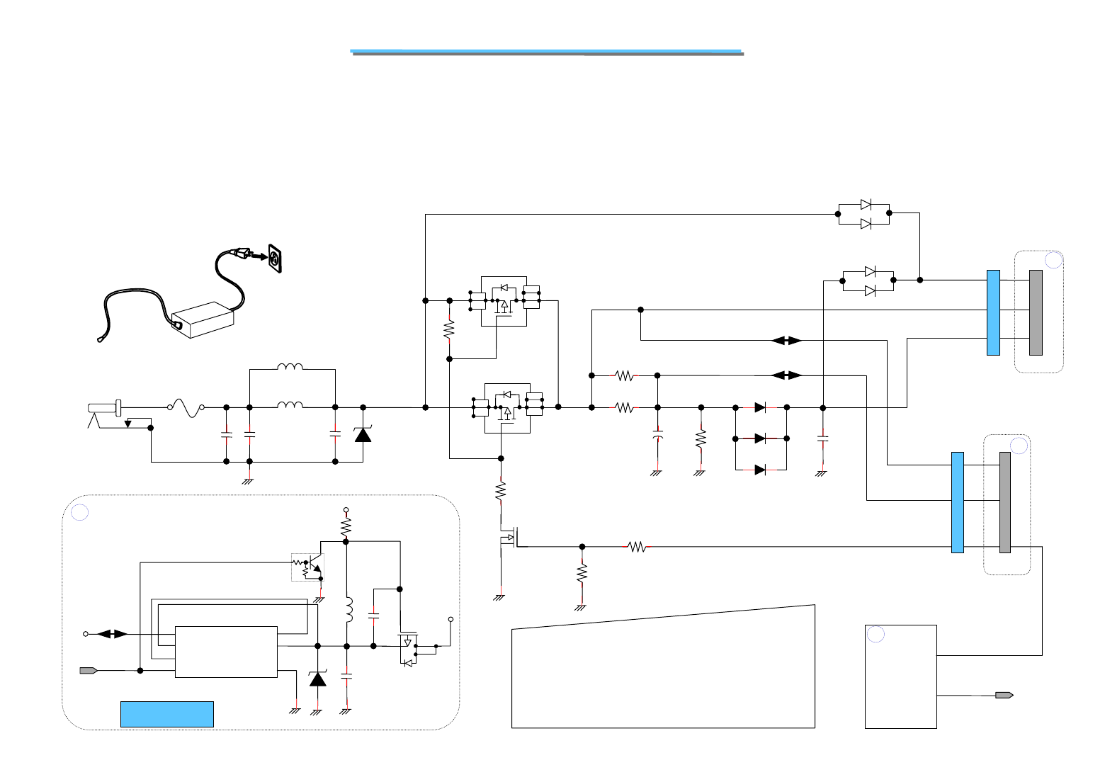
145
8170 N/B MAINTENANCE
POWER IN
J5
PF501
6.5A/32VDC PL503
120Z/100M
PC505
1U
PC510
0.1U
PD501
RLZ24D
PC509
0.1U
1
2
PR5
470k
PQ1
2N7002 G
S
D
PL502
120Z/100M
PR4
470K
PQ502
SI4835DY
S
D
2
3
1
6
7
8
5
G
S
D
2
3
1
6
7
8
5
G
PQ503
SI4835DY
PR514 .1
PR513 .1
PC19
100U
PR10
10K
PD6
PD5
PD4
PC17
0.1U
1
2
3
3
JL2
JL3
PJ1
ALWAYS
ADINP
ADINP_1
ADINP_2
DVMIAN
8
1
2
1
10,12
PJ2
PR6
100K
PR9 47K
3
LEARNING
IN
SENSE
FB
SHUTDN
5VTAP
OUT
ERR-
GND
PU7
JS7 8
2
7
PQ1
S1231DS
S
G
D
PL8
+5VA
ALWAYS
PC24
10U
3
2
1
+5V
PQ2
3
6
1
4
J3
J6
MB
MB
PD2
PD3
U508
H8
F3437
12 LEARNING
3
2
1
Step1 : Connect Adaptor to ( D/D BD ) J5 & O/P “ALWAYS”.
Step2 : “ALWAYS” --> PU7 Generate +5VA.
Step3 : H8 O/P “LEARNING” for Charger Circuitry.
Step4 : For MOSFET “PQ502&PQ503” G=0,D<-->S.
Step5 : O/P “ADINP”& “DVMAIN”.
SW_+5VA
19 SW +5VA
Mother Board
PD7
From H8
PR16
470K
PC26
0.1U
P20
P19
P22
P22
8.1 No Power (2)
When the power button is pressed, nothing happens, no fan activity is heard and power indicator is not light up.
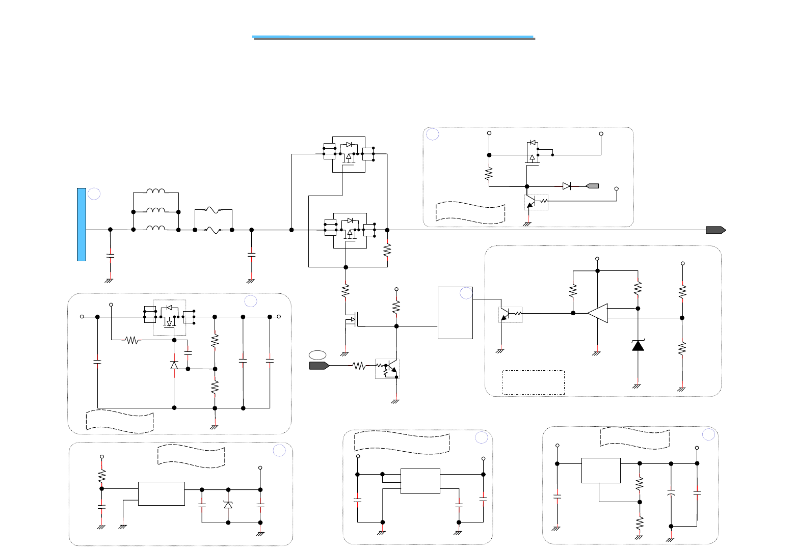
146
8170 N/B MAINTENANCE
PC32
0.01U
J28
PL11 120Z
PL10 120Z
PL9 120Z
PF2
PF1
PC30
0.1U
PU10
SI4835DY
S
D
2
3
1
6
7
8
5
G
PU11
SI4835DY
Battery Connector
G
S
D
PR554
1M
PR559
100K
1,2
PR563
100K
PQ508
2N7002
U508
H8
F3437
30
-ADEN
DBATT
2
3
1PQ509
DTC144WK
+5VA
DVMAIN
+
-
+5VAS
3
8
2
1
PR567
100K
PR572
100K PR564
475K
PU513A
LMV393M
4
PR566
100K
PQ510
SCK431
ADINP
P22
47
3
1BATT_DEAD
2
S
D
2
3
1
6
7
8
5
G
PR23 4.7K
PQ3
SCK431LCSK-5
+3V
PR22
4.7K
PR24
4.7K
PC42
470P
+12VS
+1.5VS
PC44
10U
PC45
0.1U
S
G
D
3
1
-ADEN(From H8)
PD503
PQ511
1
+5VA +5VAS
+3V
PQ512
PR573
100K
VIN
GND
EN
OUT
BYP
15
3
+3V_ICH +1.8V-ICH
24
PU514
PC559
1U PC560
0.01U
AME8801
MEEV
VIN VOUT
GND/ADJ
1
3
+3VS +1.8VS
2
PU12
AMS1085
PC37
4.7U
PC10
0.1U
PR20
560
PR19
1.2K PC9
100U
+5VA---->+5VAS
+3VS ----> +1.8VS
+3V_ICH ----> +1.8V_ICH
+3V---->+1.5VS
Q510
DTC144TKA
+3V_ICH
D8
RLZ3.6B
PC27
4.7U
PC22
0.1U
VOUT
VIN
GND
3
1
+5V
PR616
0
PC29
4.7U
2
PU8
+5V---->+3V_ICH
S
D
2
3
1
6
7
8
5
G
P20
PU13
AO4400
PC43
10P
P21
P20
PC558
4.7U
P21
P19
P21
P20
8.1 No Power (3)
When the power button is pressed, nothing happens, no fan activity is heard and power indicator is not light up.
DVMAIN
Battery OVP
PR561
169K
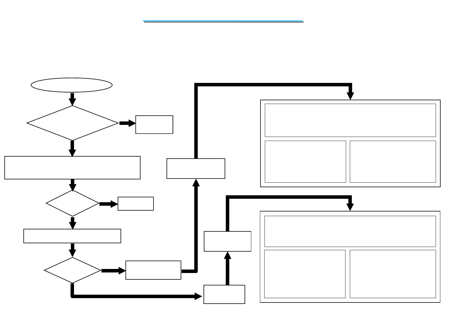
147
8170 N/B MAINTENANCE
Board-level
Troubleshooting
Replace
Motherboard
Battery can not Charge
Connect
AC adaptor.
Replace the
faulty D/D Board
No
Yes
No
Try another known good D/D Board.
Yes
Yes
Is the
notebook connected
to power (AC adaptor)?
No
1. Make sure that the battery is good.
2. Make sure that the battery is installed properly.
3. Check the D/D board is connected to M/B properly.
Correct it.
Power
OK?
Power
OK?
Board-level
Troubleshooting
Check the following parts for cold solder or one of the following
parts on the D/D Board may be defective, use an oscilloscope
to check the following signal or replace the parts one at a time and
test after each replacement.8
Parts Signal
J5 PL502 PL503 PD[501:503]
PQ1 PR5 PR9 PR514
PR513 JL2 JL3 PD[2:6]
PJ1 PJ2 J6 U508
ALWAYS ADINP
DVMAIN ADINP_1
ADINP_2 LEARNING
Check the following parts for cold solder or one of the following
parts on the mother-board may be defective, use an oscilloscope
to check the following signal or replace the parts one at a time and
test after each replacement.
Parts Signal
PU7 PQ2 PL8 PQ1
J28 PL[9:11] PF1 PF2
PU10 PU11 PR554 PR559
PQ[508:510] U508 Q510
PU513 PR567 PR572
PR564 PR566
+5VA SW_+5VA
DBATT ADINP
-ADEN BATT_DEAD
DVMAIN
8.1 No Power
When the power button is pressed, nothing happens, no fan activity is heard and power indicator is not light up.
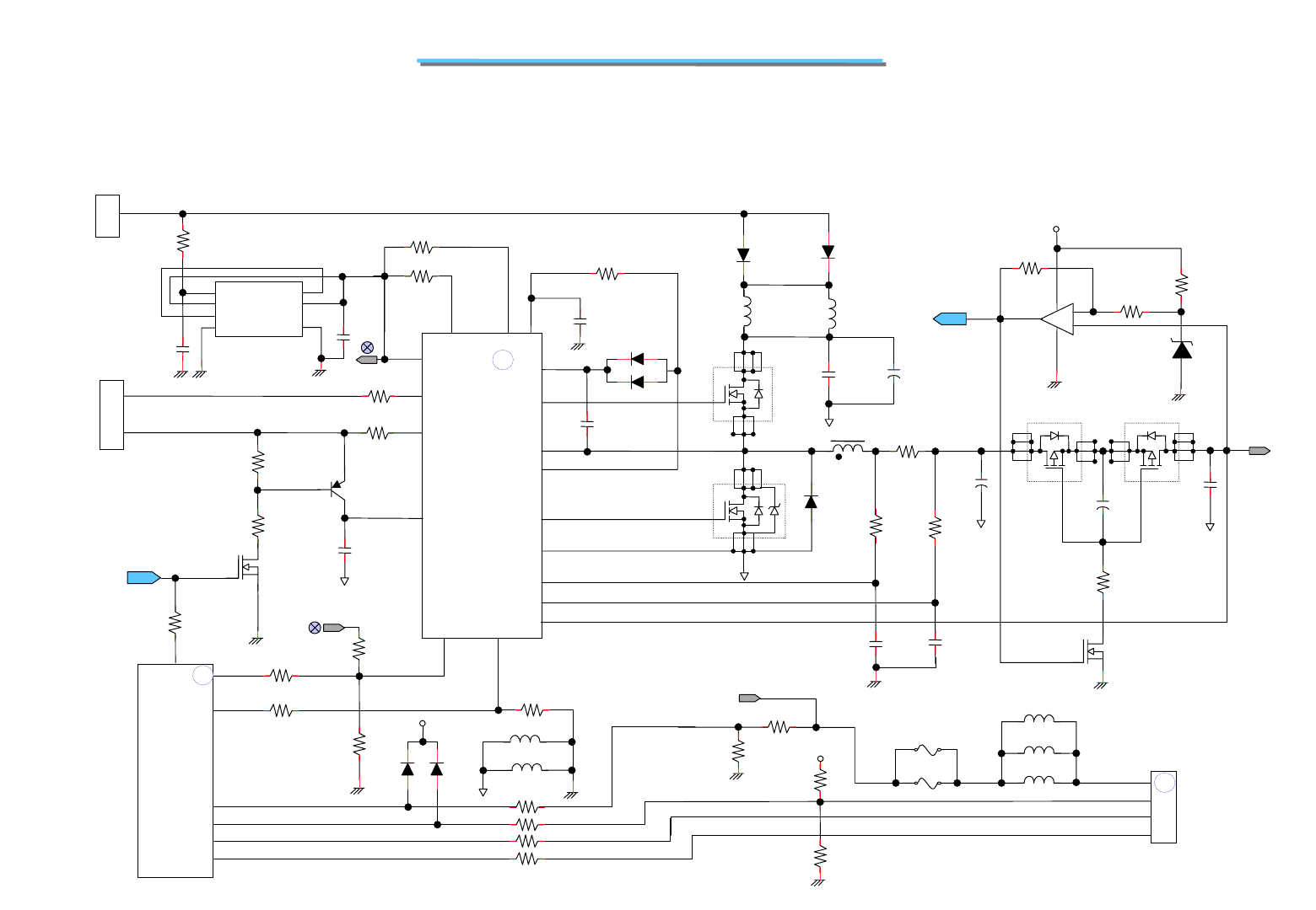
148
8170 N/B MAINTENANCE
8.2 Battery Can not Be Change
When the battery is installed but the battery status indicate LED display abnormal.
S
D
23
1
67
8
5
G
G
S
D
E
C
B
PQ506
2N7002
PR547
33K
PR553
47K
PC553
1U
PQ505
BT3906
PR546
10K
PR552 10
PR548 10
ADINP_2
ADINP_1
1
2
S
D
231
67
8
5
G
3
PD502
PU5
PU6
4
4
PC551
1U
PR557 33 PD5 PD4
PL5 PL6
PC20
10U
PC18
100U
PC542
0.1U
PD6
PL7 PR13
0.035
PC23
100U
S
D
2
3
1
6
7
8
5
GSD
2
3
1
6
7
8
5
G
PU512 PU9
PR551
1M
PR556
1M
G
S
D
PR14
1M
PR15
1M
PC539
0.1U
PC538
0.1U
17
18
19
20
21
22
23
24
25
2
1
27
26
8
2
7
3
6
1
4
IN
F/B
SENSE
SHUTDN
5VTAP
OUT
GNT
PU510
LP295
PC536
0.1U
PC535
4.7U
15
PR534 100K
16
CHARGING
PR615 0
PR555
12.1K
PL14
PR541 100K
13
VCTL
REFIN
CSSN
CSSP
DCIN
ICTL
PR536
10K
PR539 1K
PR537
47K
PL15
14 28
IINP
BATT
CSIN
CSIP
PGND
DL0
DL0V
LX
DHI
BST
LD0
CELLS
+
-
+5VAS
5
8
6
7
PR572
100K
PU513B
LMV393M
4
PQ510
100K
PR570 12.1K
PR569
1M
DBATT
PC28
10U
DBATT
PL11 120Z
PL10 120Z
PL9 120Z
PF2
PF1
+5VAS
PR17
20K
PR18
4.99K
PR565
100K
PR562
301K
BAT_T
BAT_V
69
44
40
U508
H8
F3437
39
38
99
23
1,2
3
4
5
BAT_C
BAT_D
27
1
3
4
8
6
5
RP518 33*4
+5VA
D510
3
21
J28
Battery Connector
DBATT
LI_OVP
LI_OVP
BAT_VOLT
BAT_TEMP
BAT_CLK
BAT_DATA
PU511
MAX1772
J3
10,12
J6
1
2
PQ507
2N7002
P22
P19
P20
PR532
10
ADINP
D/D Board
connector
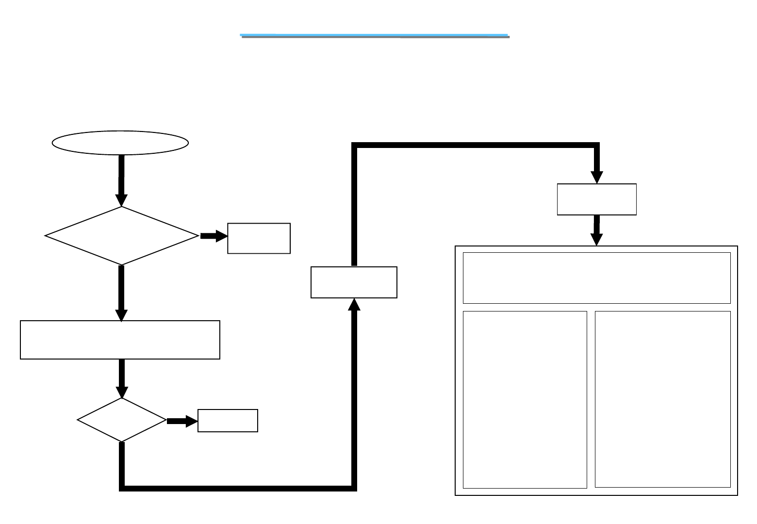
149
8170 N/B MAINTENANCE
Battery can not Charge
Connect
AC adaptor.
No
Yes
No
Yes
Is the
notebook connected
to power (AC adaptor)?
1. Make sure that the battery is good.
2. Make sure that the battery is installed properly.
Correct it.
Battery charge
OK?
Check the following parts for cold solder or one of the following
parts on the mother-board may be defective, use an oscilloscope
to check the following signal or replace the parts one at a time and
test after each replacement.2
Parts Signal
J3 J6 PU510
PR548 PR552
PQ505 PQ506
PR546 U508
PU511 PR557
PR534 PR541
PD502 PC542
PU5 PU6
PD[4:6] PL[5:7]
PL[9:11] PF[1:2]
PQ507 J28
PR556 PU513
PQ510 PR570
PR569 PU512
PU9
ADINP
ADINP_1
ADINP_2
LI_OVP
CHANGING
DBTT
BAT_T
BAT_C
BAT_D
Board-level
Troubleshooting
Replace
Motherboard
8.2 Battery Can not Be Change
When the battery is installed but the battery status indicate LED display abnormal.
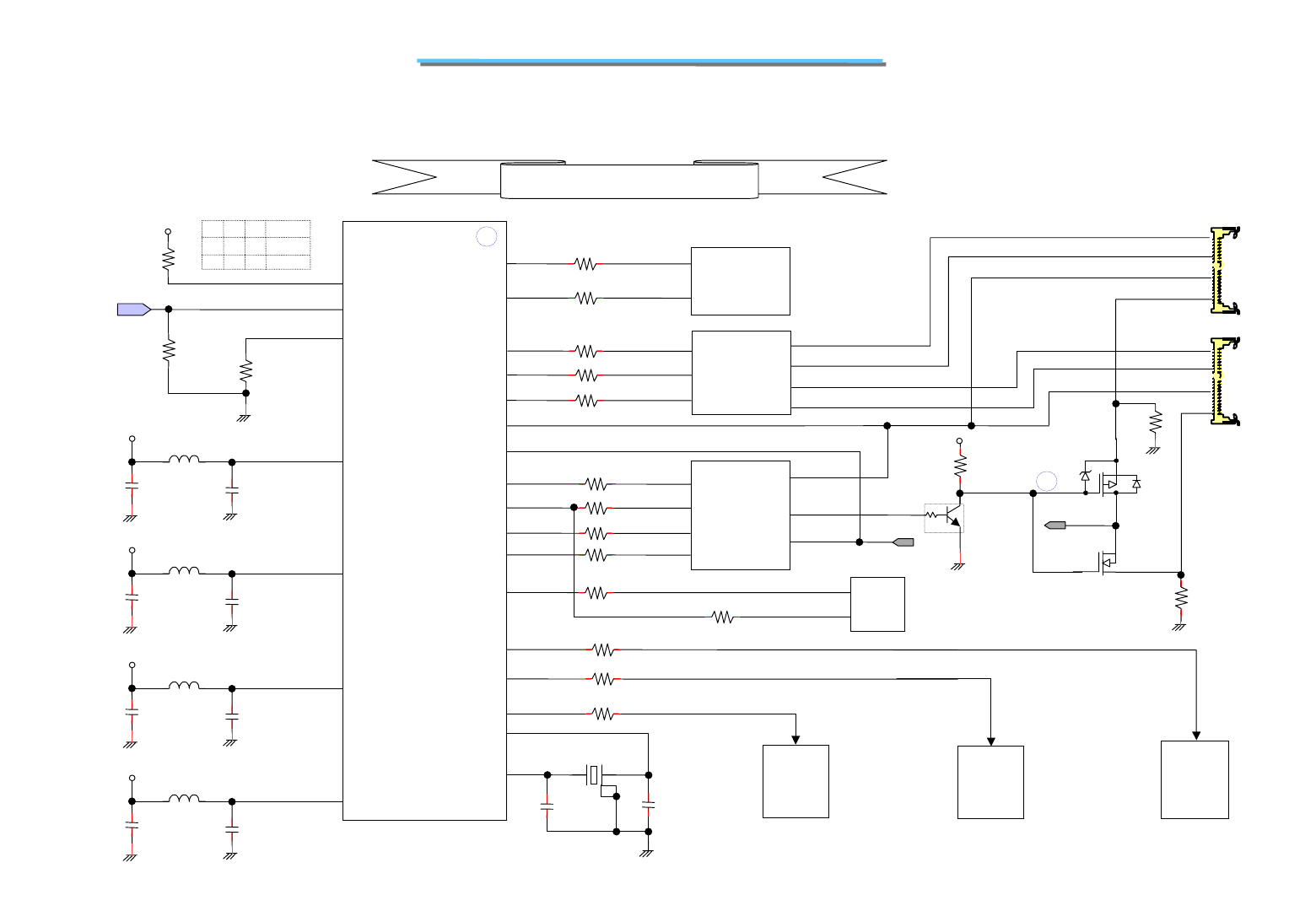
150
8170 N/B MAINTENANCE
8.3 No Display
R592 33
52 HCLK_CPU
R594 33
51 -HCLK_CPU
R608 33
45 HCLK_MCH
R612 33
41 -HCLK_MCH
R621 33
21 66M_MCH66IN
R624 33
39 USBCLK_ICH
R596 33
56 14M_ICH
R616 33
13 PCICLK_ICH
R620 33
22 66M_ICH
SMBCLK
SDRAMCLK0
SDRAMCLK1
SDRAMCLK4
SDRAMCLK5
SMBDATA
DRAMENA 3
1
2
D
S
G
S
G
D
D
SMBDATA
21
21
SMBCLK
SMBDATA
R51 10K
+5V Q7
FDV302
J503
J505
Q8
FDV302
61
74
142
141
61
74
142
141
12 R609 33 PCICLK_LPC
SIO_14.318MHZ
R595 33 20
8
U509
PC87383
U516
MOBILITY
-M6
23 R626 33 66M_AGP
11 R610 33 PCICLK_LAN
U4
RTL8139CL
10 R607 33 PCICLK_CARD
U7
PCI4410
HK
U3
Brookdale-
MCH82845
U17
ICH2
82801BA
3
2
4
X502
3
C617
5P
C618
5P
2
14.318M
U507
ICS950805
U1
Pentium 4
System Clock Check
SMBDATA1
SMBDATA0
Q6
DTC144TKA
R169
100K
R168
100K
P8
P9
+3VS
R45
1K
R50
1K
R44
1K
54
55
40
From
CPU
FS0
FS1
FS2
H_BSEL
+3VS L517
120Z/100M
C626
0.1U
C625
2.2U
+3VS L516
120Z/100M
C619
0.1U
C622
2.2U
+3VS L518
120Z/100M
C645
0.1U
C649
2.2U
+3VS L519
120Z/100M
C641
0.1U
C646
2.2U
+3VCLKCPU 46,50
+3VCLKPCI 8,14
+3VCLKNA 1,26,37
+3VCLK66 19,32
FS2 FS1 FS0 CPUCLK
0
0
0
1
1
1
100MHz
133MHz
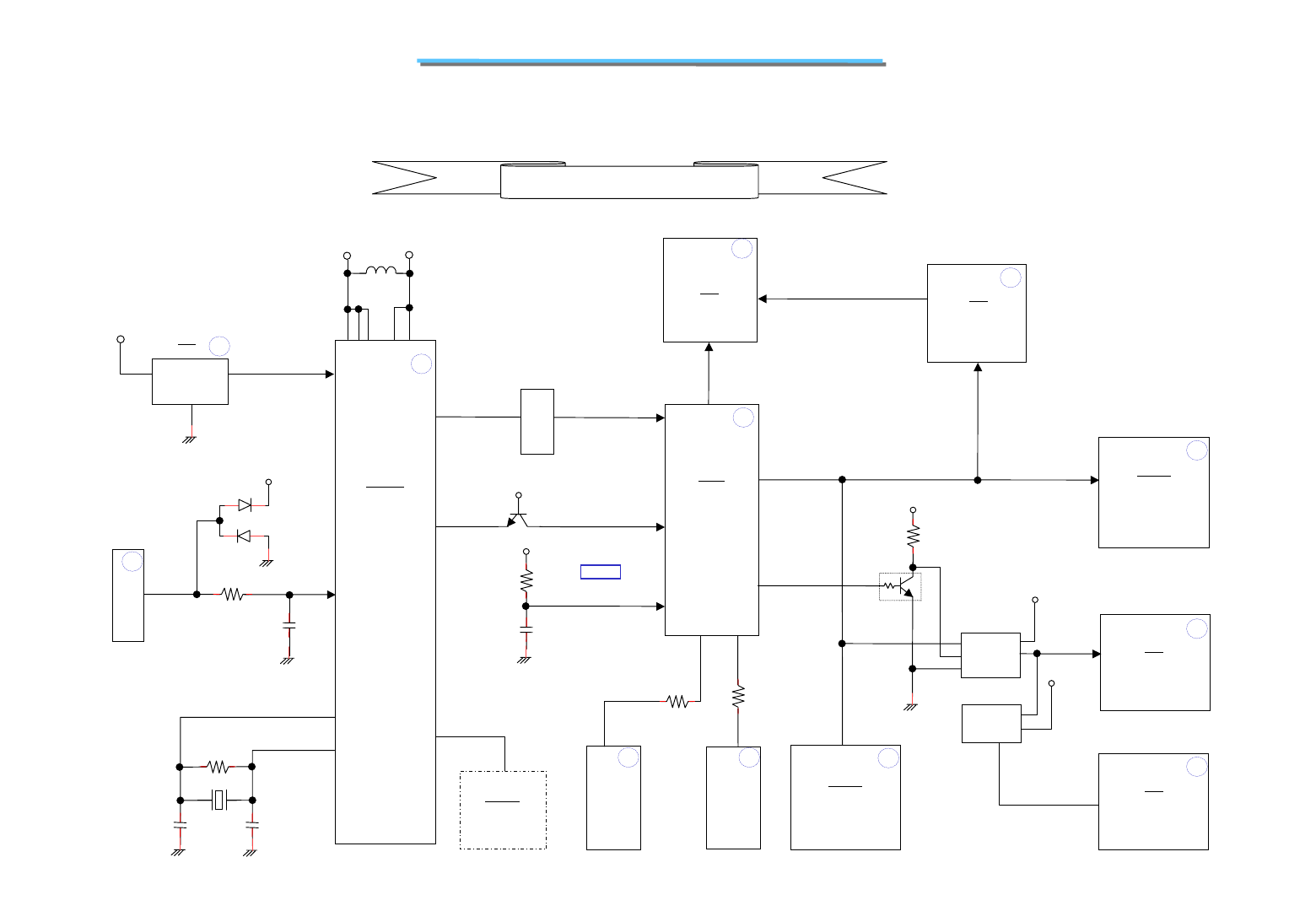
151
8170 N/B MAINTENANCE
System Reset Check
8.3 No Display
VCC
GND
RESET#
3
1
2-H8_RESET
U508
Micro
Controller
H8/F3437
8170
Power
Module
1
14
-POWERBTN
1
3
2
23
Easy Start
Button
5
J5
P19
459937
+5VA
L520
36
H8_VDD5
P19
+5VA U10
MAX809
H8_PWROK
H8_PWRON
P19
R617 1K
-PWRSW
D505
BAV99
+5VA
C634
.01U
Level Shift
5
21 4
U13
SN74CBTD3384
PWROK
18 -H8_ICH2BIN
Q513
DTC144TKA
+5V
-PWRBTN
+5V
R100
10K
C181
1U
-RSMRST
Tr>10ms
2
3
R627 1M
X503 16MHZ
C633
68P
C630
68P
U17
ICH2
82801BA
U1
Pentium 4
H_PWRGD
-PCIRST
-PCIRST
U3
MCH
82845
U516
VGA
M6
U4
LANPHY
U509
PC87393
-PCIRST
-PCIRST
9
Q15
DTC144TKA
A
B
GNT
VCC
Y4
+3V
5
+3V_ICH
U16
R158
4.7K
1
2
3
115
-CPURST
J10
Secondary
EIDE
Connector
R56 33 R55
33
J14
Primary
EIDE
Connector
15
-BRSTDRV1
-BRSTDRV2
-CDROM_RST
-HDD_RST
P13
P13
P10
P18
-PCIRST_MSK
U7
PCI14410GHK
-PCIRST_N
A
Y
+3V
VCC 5
1
4
-CBRST
P15
U8
NC7S08
NC7S08
P7
P4
P14 P14
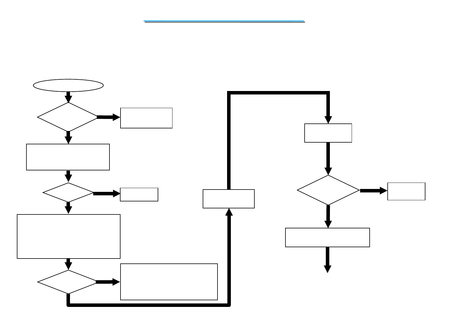
152
8170 N/B MAINTENANCE
8.3 No Display
There is no display on both LCD and VGA monitor after power on although the LCD and monitor is known-good.
No Display
Replace monitor
or LCD.
Board-level
TroubleshootingYes
No
Monitor
or LCD module
OK?
Make sure that CPU module,
DIMM memory are installed
Properly.
Display
OK?
Yes
No
Correct it.
To be continued
Clock and reset checking
Check system clock and reset
circuit.
Replace
Motherboard
1.Try another known good CPU
module, DIMM module And BIOS.
2.Remove all of I/O device (FDD,
HDD, CD-ROM…….) from
motherboard except LCD or monitor.
Display
OK?
1. Replace faulty part.
2. Connect the I/O device to the
M/B one at a time to find out
which part is causing the problem.
Yes
No
If 378 Port
Have error code
No
According error
Cord to repair
Yes
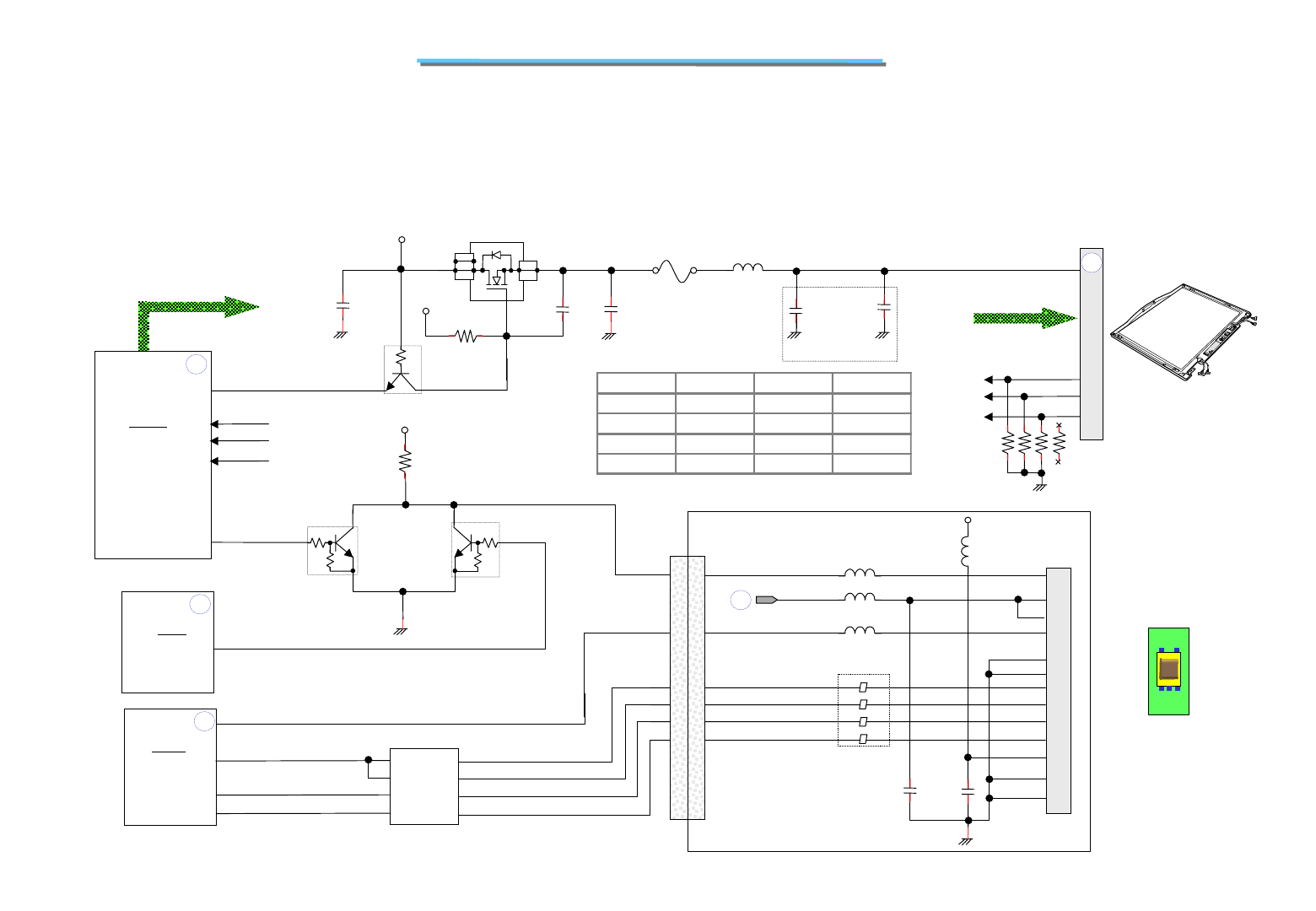
153
8170 N/B MAINTENANCE
3
1
2
2
R1
3
1
8.4 VGA Controller Failure LCD No Display
There is no display or picture abnormal on LCD or monitor.
Q500
NDS9410
S
D
2
3
1
6
7
8
5
G
C507
0.1U
3
1
2
LCD
BKL_VMAIN
Inverter Board
J6
U508
Micro
Controller
H8/F3437
ENPVDD
U516
VGA-M6
MOBILITY
M6
C512
10U
LCDVCC
J2
Close to LCD
Connector
TXCLK+, -
TX2CLK+, - TXOUT [0:2]+ ,-
TX2OUT [0:2]+, - TXCLK+ -
TX2CLK+ -
TXOUT [0:2]+ -
TX2OUT [0:2]+ -
Inverter
F502
SMDC110
+12V R515
470K
Q502
DTC144WK
+3VS
C506
0.1U
L505
120Z/100M
C503
0.1U
C1
1000P
1
2
3
4
5
6
7
9
8
10
11
8
7
6
5
1
2
3
4
FA501
L507
L510
L509
L508
+5VAS
PJ2
ENPBLT1
7
8
J6
15
13
11
9
BLADJ
-AC_POWER
-BATT_LED
-BATT_G
-BATT_R
GND1
GND2
P1
C512
0.1U
C513
0.1U
10
11
12
13
QE
QF
QG
QH
A
B
CLK
CLR
-AC_POWER
-BATT_LED
-BATT_G
-BATT_R
U514
LED_DATA 1
2
8
9
LED_CLK
-H8_RESET
90
91
1
15
13
11
9
8
BLADJ
45
-ENABKL
+3VS
P10
U17
ICH2
82801BA
1,2
Q3
DTC144WK Q12
DTC144WK
R22
10K
-ENABKL_MSK
7
LCD_ID0
LCD_ID1
LCD_ID2
31
33
35
LCD_ID0
LCD_ID1
LCD_ID2
DISPLAY LCD_ID2 LCD_ID1 LCD_ID0
UNIQAC 001
HYUNDAI 010
HANNSTAR 011
CMO 100
P13
P19
D/D Board
RP520
47K*4
1
2
34
5678
P12
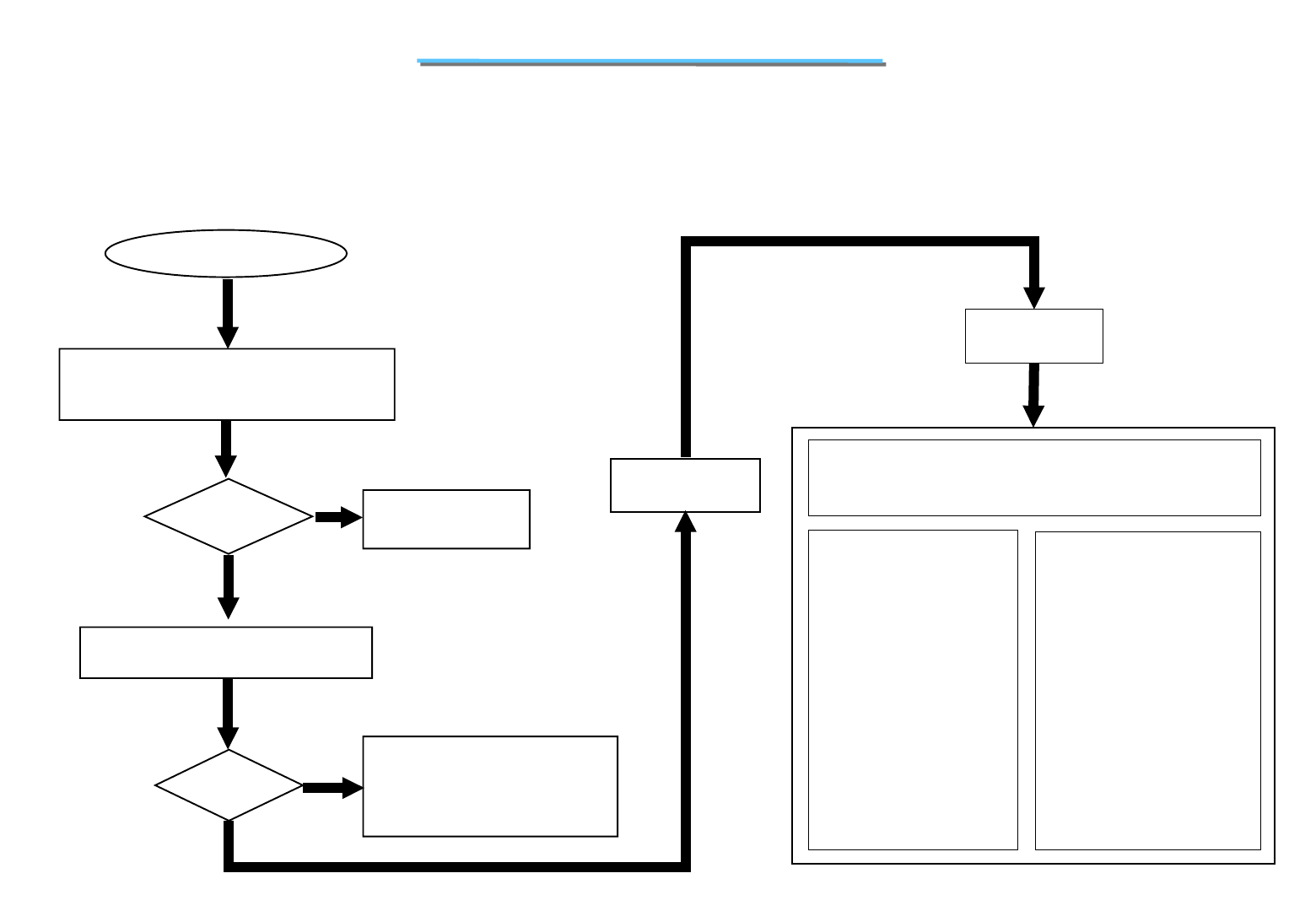
154
8170 N/B MAINTENANCE
Replace faulty
LCD
VGA Controller Failure
1.Confirm monitor is good and check the cable
are connected properly.
2. Try another known good LCD
Display
OK?
Remove all the I/O device & cable from
motherboard except extended LCD.
Display
OK?
Connect the I/O device & cable
to the M/B one at a time to find
out which part is causing the
problem.
Yes
No
Yes
No
Board-level
Troubleshooting
Replace
Motherboard
One of the following parts on the mother-board may be
defective, use an oscilloscope to check the following signal or
replace the parts one at a time and test after each replacement.
Parts: Signals:
-AC_POWER
-BATT_LED
-BATT_R
-BATT_G
-ENABLE_MSK
-ENABKL
EVPVDD
TXCLK[+:-]
TX2CLK[+:-]
TXOUT[0:2][+:-]
TX2OUT[0:2][+:-]
LCDVCC
BLADJ
BKL_VMAIN
U516 U17
Q3 Q12
R22 Q502
Q500 R515
C506 C507
F502 L505
J2 D500
J1 J6
PJ2 FA501
L[508:510]
U514
L507 C513
C512
8.4 VGA Controller Failure LCD No Display
There is no display or picture abnormal on LCD or monitor.
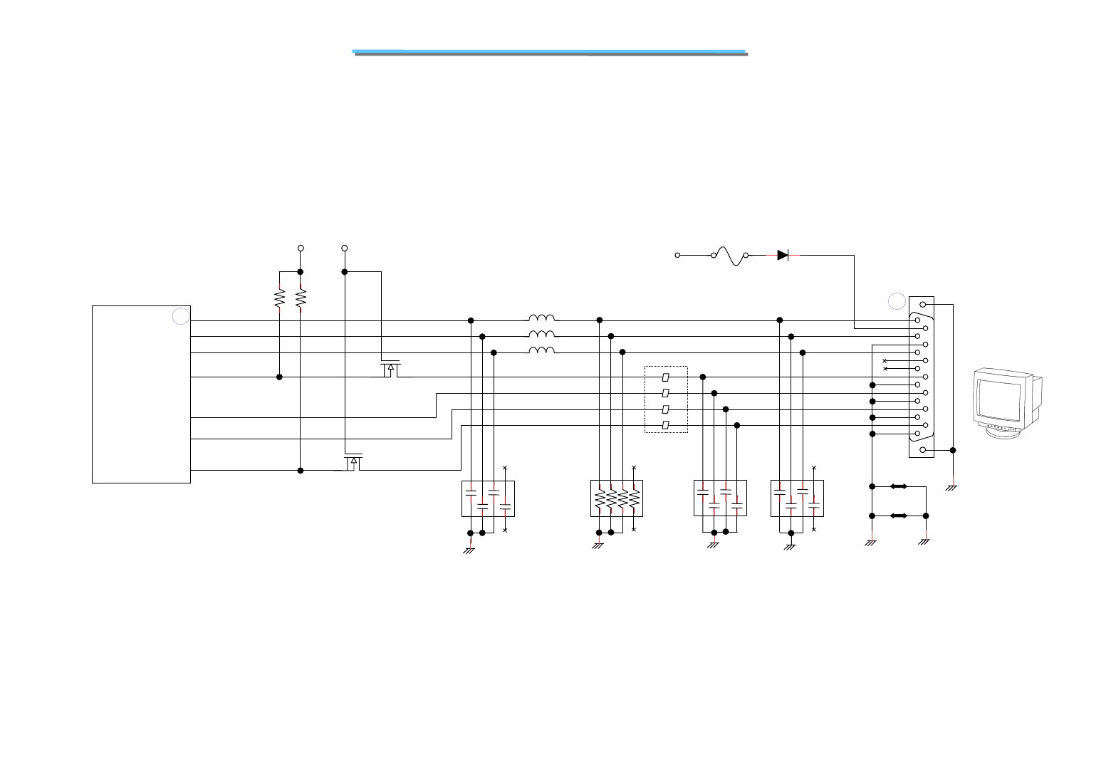
155
8170 N/B MAINTENANCE
8.5 VGA Controller Failure Monitor No Display
There is no display or picture abnormal on monitor.
MONITOR
Q502
2N7002
G
SD
+3VS
R543
4.7K
R544
4.7K
+5VS
Q501
2N7002
G
SD
4
3
2
1
5
6
7
8
4
3
2
1
5
6
7
8
4
3
2
1
5
6
7
8
RP501
75*4
4
3
2
1
5
6
7
8
CP3
22P*4
CP501
22P*4 CP500
22P*4
JL1
JL2
GND_CRT15
F501
SMDC110
DDC2B
D500
D1FS4
+5VS
120Z/100M
L500
L501
L502
120Z/100M
120Z/100M
J1
External VGA Connector
1
9
2
10
3
11
4
12
5
13
6
14
7
15
8
16
17
U516
VGA-M6
MOBILITY
M6
5
6
7
8
4
3
2
1
FA500
SCL
VSYNC
HSYNC
SDA
RED
GREEN
BLUE
P12
P10
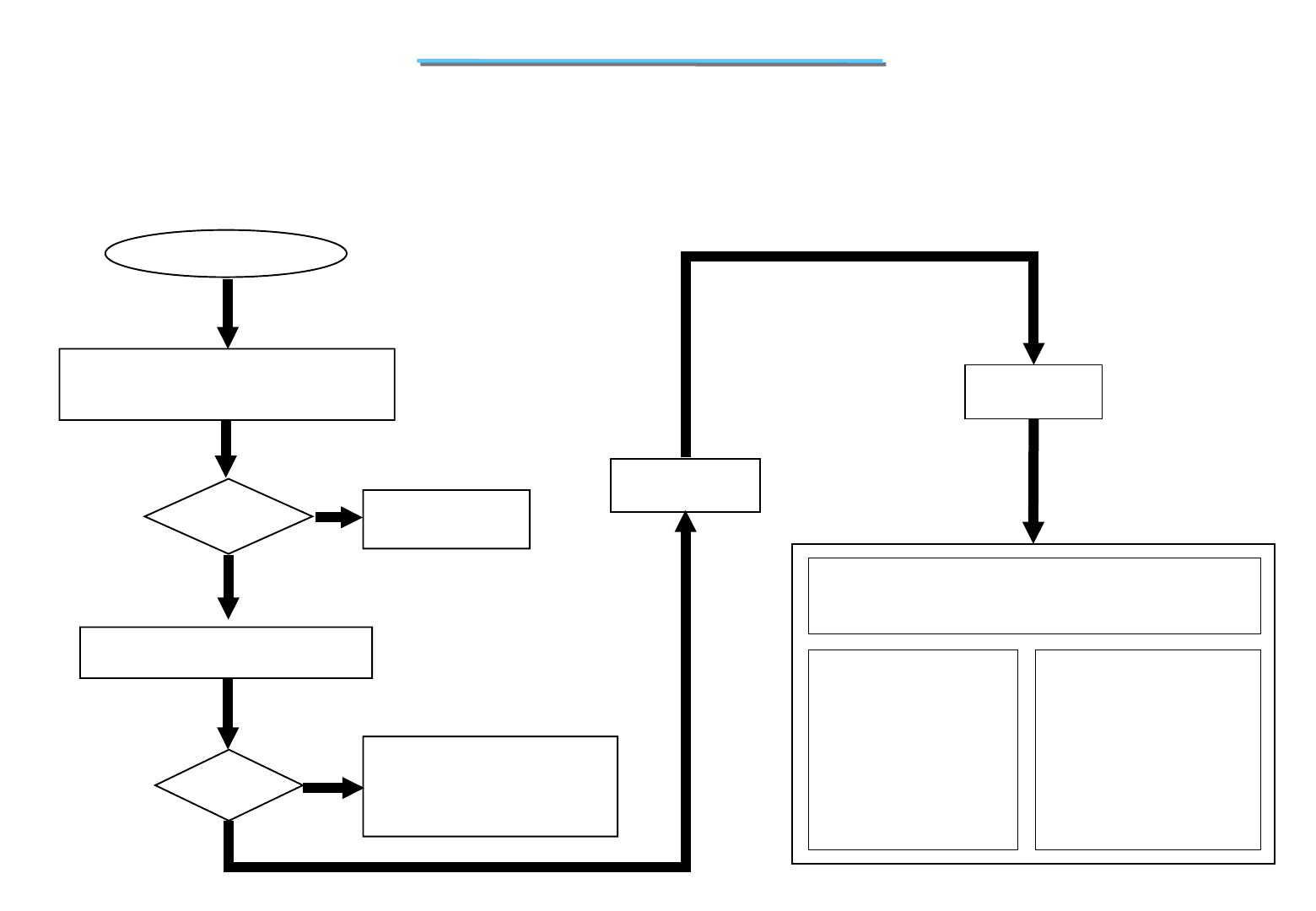
156
8170 N/B MAINTENANCE
8.5 VGA Controller Failure Monitor No Display
Replace faulty
monitor.
VGA Controller Failure
1.Confirm monitor is good and check the cable
are connected properly.
2. Try another known good monitor
Display
OK?
Remove all the I/O device & cable from
motherboard except extended monitor.
Display
OK?
Connect the I/O device & cable
to the M/B one at a time to find
out which part is causing the
problem.
Yes
No
Yes
No
Board-level
Troubleshooting
Replace
Motherboard
There is no display or picture abnormal on monitor.
One of the following parts on the mother-board may be
defective, use an oscilloscope to check the following signal or
replace the parts one at a time and test after each replacement.
Parts: Signals:
RED
GREEN
BLUE
SDA
HSYNC
VSYNC
SCL
U516 R544
R543 Q501
Q501 CP3
RP501 CP501
FA500 L500
L501 L502
CP500 F501
D500 J1
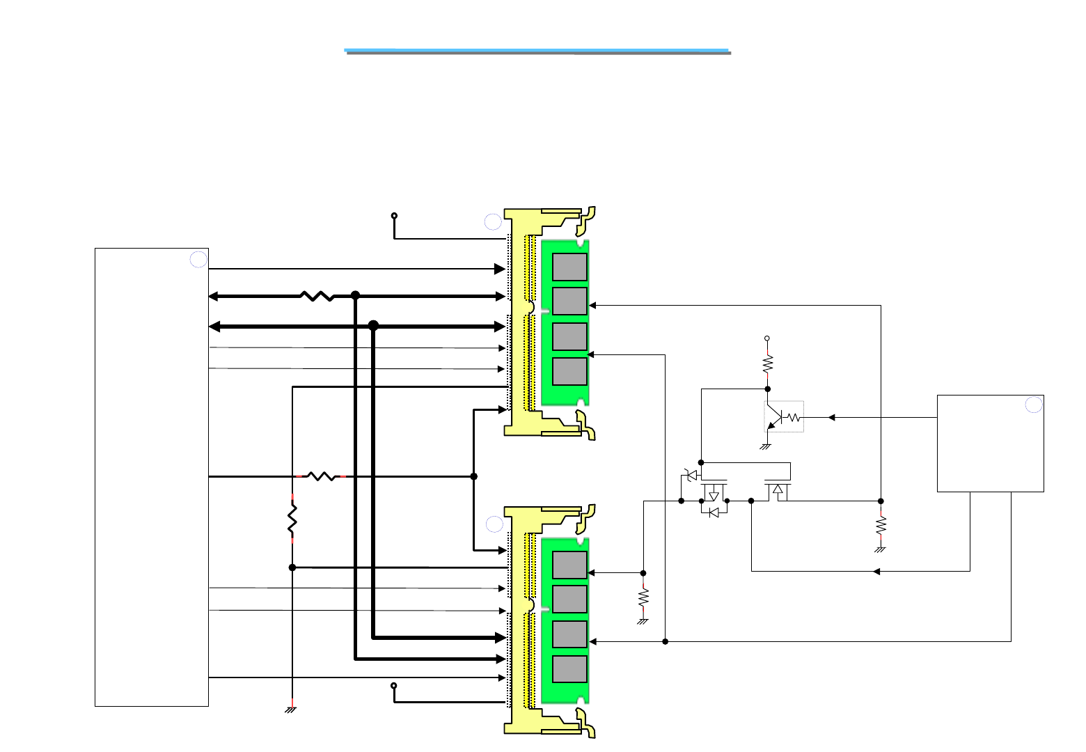
157
8170 N/B MAINTENANCE
8.6 Memory Test Error
Either one or two extend SO-DIMM RAM Module is failure or system hangs up.
J505 SO-DIMM
J503 SO-DIMM
MA [0:14]
MD [0:63]
-MCS[4:5]
-MSWEA
-MSCASA
-MSRASA
-MCS[0:1]
-MSWEA
-MSCASA
-MSRASA
-CS[0:1]
-CS[4:5]
-SWEA
-SCASA
-SRASA
CK[2:3]
CK[0:1] CKE[0:1]
CKE[2:3]
MAA [0:12]
MDD [0:63]
-MDQMA [0:7]
MAA [0:12]
MDD [0:63]
-MDQMA [0:7]
RP7,RP9
0*8
RP3
0*8
SMBCLK
G
D
S
R1
+5V
R51
10K
Q6
DTC144TKA
Q7
FDV302P
Q8
2N7002
SMBDATA1
SMBDATA
SMBCLK
DRAMENA
+3V
RP14
0*8
+3V
G
DS
SMBCLK
SMBDATA0
SMBDATA1
SDRAMCLK1
SDRAMCLK2
SDRAMCLK4
SDRAMCLK5
SDRAMCLK1
SDRAMCLK2
U17
ICH2
82801BA
SDRAMCLK4
SDRAMCLK5
U3
MCH
82845
R168
100K
R169
100K
P13
P9
P9
P7
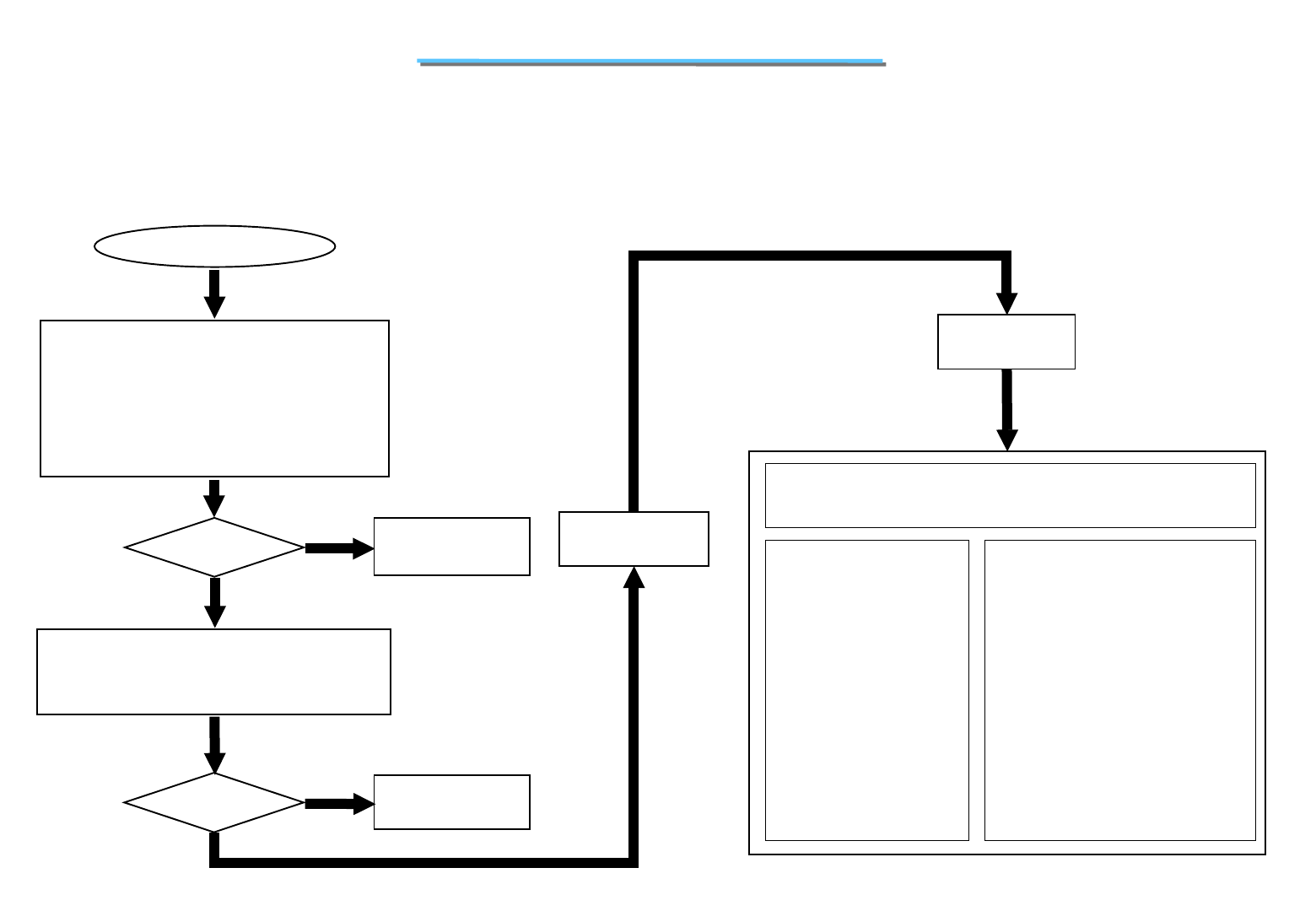
158
8170 N/B MAINTENANCE
Memory Test Error
Test
OK?
Replace the faulty
SDRAM module.
Yes
No
1.If your system installed with expansion
SO-DIMM module then check them for
proper installation.
2.Make sure that your SO-DIMM sockets
are OK.
3.Then try another known good SO-DIMM
modules.
If your system host bus clock running at
100MHZ then make sure that SO-DIMM
module meet require of PC 100.
Test
Ok?
Replace the faulty
SDRAM module.
Yes
No
Board-level
Troubleshooting
Replace
Motherboard
One of the following components or signals on the motherboard may
be defective ,Use an oscilloscope to check the signals or replace the
parts one at A time and test after each replacement.
Parts:
U3 RP7
RP9 RP3
RP14 J505
J503 U17
Q7 Q8
Q15 R51
Signals:
MD [0:63]
MDD [0:63]
MA[0:14]
MAA[0:14]
-DQMA[0:7]
-MDQMA[0:7]
-CS[0:3]
-MCS[0:3]
-SWEA
-MSWEA
-SCASA
-MSCASA
-SRASA
-MSRASA
CK[0:3]
CKE[0:3]
SDRAMCLK1
SDRAMCLK2
SDRAMCLK4
SDRAMCLK5
SMBCLK
SMBDATA
SMBDATA0
SMBDATA1
DRAMENA
8.6 Memory Test Error
Either one or two extend SO-DIMM RAM Module is failure or system hangs up.
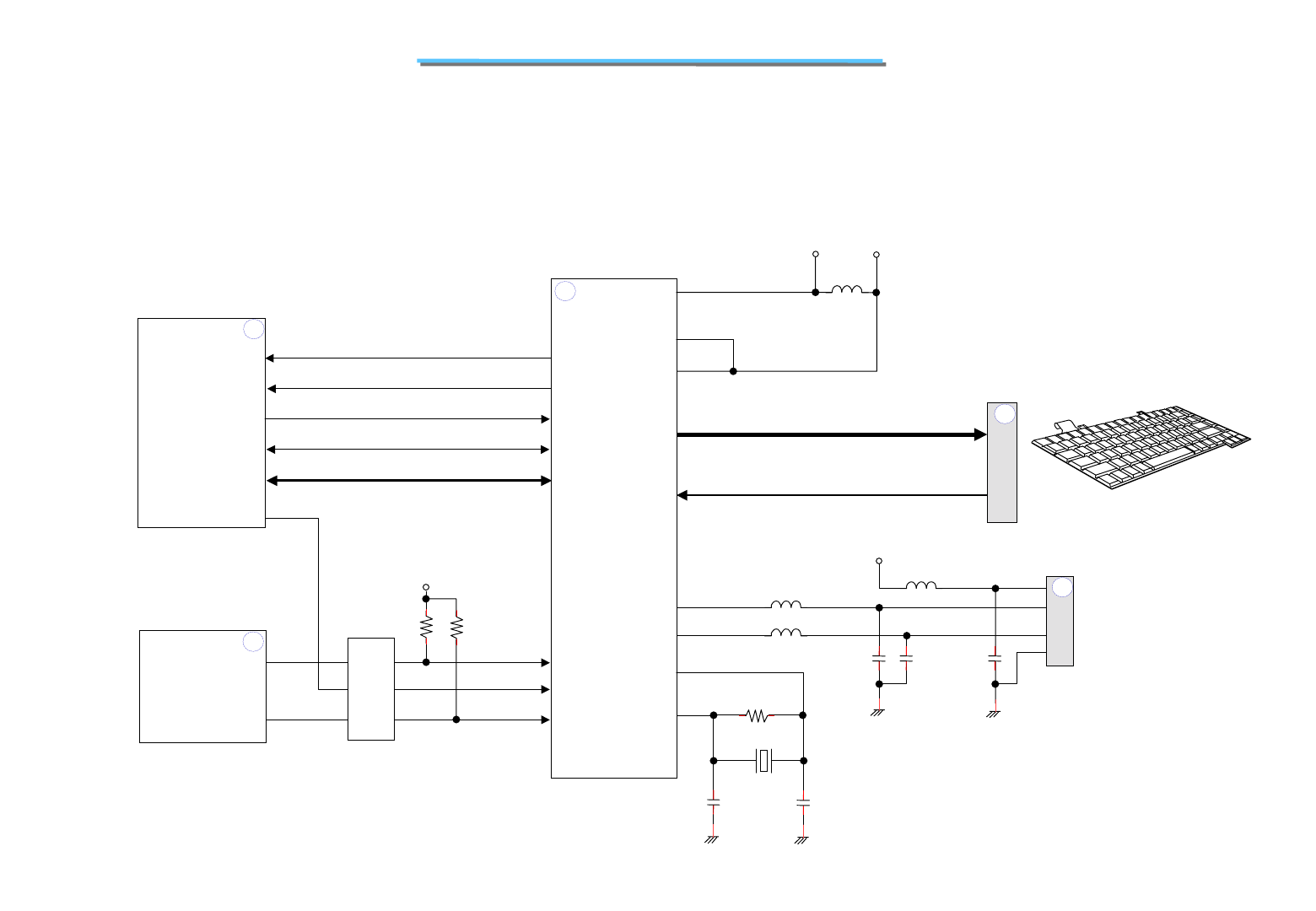
159
8170 N/B MAINTENANCE
8.7 Keyboard (K/B) Touch-Pad (T/P) Test Error
Error message of keyboard or touch-pad failure is shown or any key does not work.
U508
Micro
Controller
H8/F3437
IRQ1
IRQ12
-IOW
XD[0:7]
-IOR
Level Shift
R78
10K
+5VA
-H8_KBCS
-ROMCS 89
-H8_A20GATE
ICH-A20GATE
76
U13
74CBTD3384
2
3
Internal Keyboard Connector
J12
KO[0:15]
KI[0:7]
H8_VDD5
36
9,59,4
53
54
96
97
95
17
U17
ICH2
82801BA
U509
Supper I/O
PC87393 14 15 98
-MCCS -H8_MCCS
T_CLK
T_DATA
Touch-pad
Oonnctor
J15
+5V
L15
L16
120Z/100M
120Z/100M
L13 120Z/100M
C149
47P C139
47P C135
0.1U
4
2
3
1
57
10
R627 1M
X503
16MHz
C630
68P
C633
68P
L520
37
+5VA
R66
10K
120Z/100M
P13
P19
P19
P19
72
73
P18
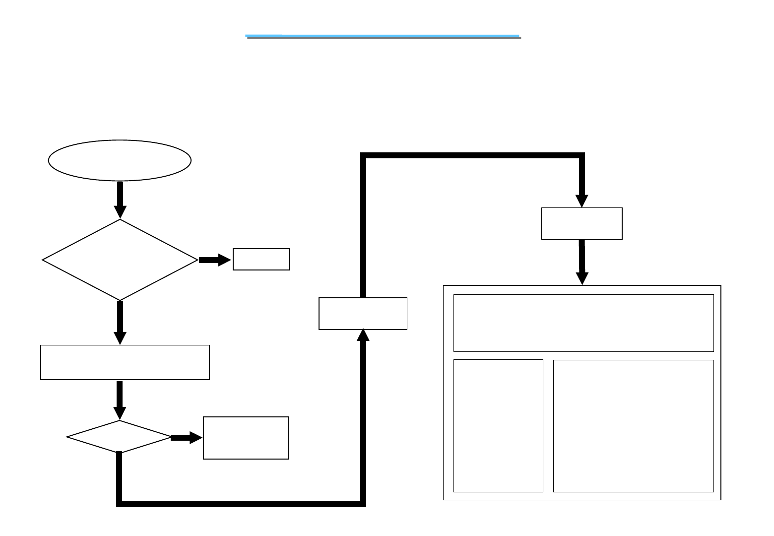
160
8170 N/B MAINTENANCE
Keyboard or Touch-Pad
Test Error
Try another known good Keyboard
or Touch-pad.(Internal or external)
Test
Ok?
Replace the faulty
Keyboard or
Touch-Pad
Yes
No
Yes
No Correct it.
Is K/B or
T/P cable connected to
notebook
properly?
Board-level
Troubleshooting
Replace
Motherboard
One of the following parts or signals on the motherboard
may be defective, use an oscilloscope to check the signals or
replace the parts one at a time and test after each replacement.
Parts
U17 U509
U13 R78
U508 L520
J12 L13
L15 L16
X503 R627
C633 C630
C149 C139
C135 J15
Signals
IRQ1
IRQ12
-IOR
-IOW
XD[0:7]
-H8_KBCS
-H8_A20GATE
-H8_MCCS
KO[0:15]
KI[0:7]
T_CLK
T_DATA
XTAL
EXTAL
8.7 Keyboard (K/B) Touch-Pad (T/P) Test Error
Error message of keyboard or touch-pad failure is shown or any key does not work.
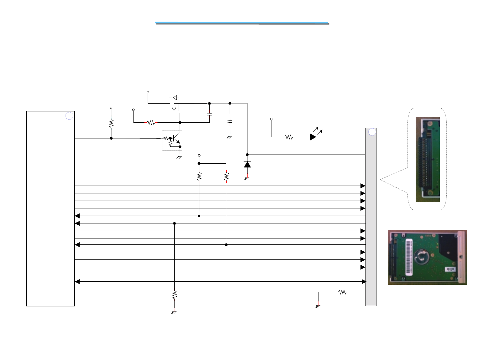
161
8170 N/B MAINTENANCE
8.8 Hard Drive Test Error
Either an error message is shown, or the driver motor continues spinning, while reading data is from or
writing data is to hard drive.
U17
ICH2
82801BA
-HDD_RST
J21
1
+3VS
-PDACK
PDA1
PDA0
PIORDY
PDREQ
-PDIOW
-PDIOR
IRQ14
-PCS1
-PCS3
PDA2
PDD [0:15] DD [0:15]
-PDACK
PDA1
PDA0
PIORDY
PDREQ
-PDIOW
-PDIOR
INTRQ
-PCS1
-PCS3
PDA2
+5VS
R156
470
D12
PG1102W
R49
470
28
31
37
38
36
25
23
21
27
35
33
29
39
-HDDACTP
Primary EIDE Connector
For Hard Disk
G
DS
+12VS
R138
10K
R137 1M
-HDD_PWRON
+5VS
Q14
DTC144WK
Q13
DTC144WK
C182
4.7U
C201
0.1U
-HDDRST
+5VS
R91
10K
R84
4.7K
R71
5.6K
41,42
D513
EC10QS04
P14
P13
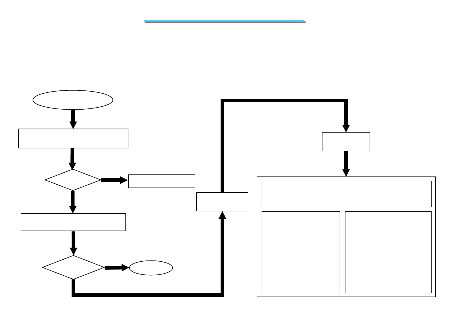
162
8170 N/B MAINTENANCE
Hard Driver
Test Error
Yes
No
Re-boot
OK? Replace the faulty parts.
1. Check if BIOS setup is OK?.
2. Try another working drive and cable.
Check the system driver for proper
installation.
No
Re - Test
OK? End
Yes
Replace
Motherboard
One of the following parts or signals on the motherboard may be
defective, use an oscilloscope to check the signals or replace the parts
one at a time and test after each replacement.
PARTS: SIGNALS:
U17 R138
Q13 Q14
R137 C201
C182 R84
R91 R71
R156 J21
-HDDRST -PDACK
PDA1 PDA0
PIORDY PDERQ
-PDIOW -PDIOR
IRQ14 -PCS1
-PCS3 PDA
PDD[0:15]
-HDD_PWRON
Board-level
Troubleshooting
8.8 Hard Drive Test Error
Either an error message is shown, or the driver motor continues spinning, while reading data is from or
writing data is to hard drive.
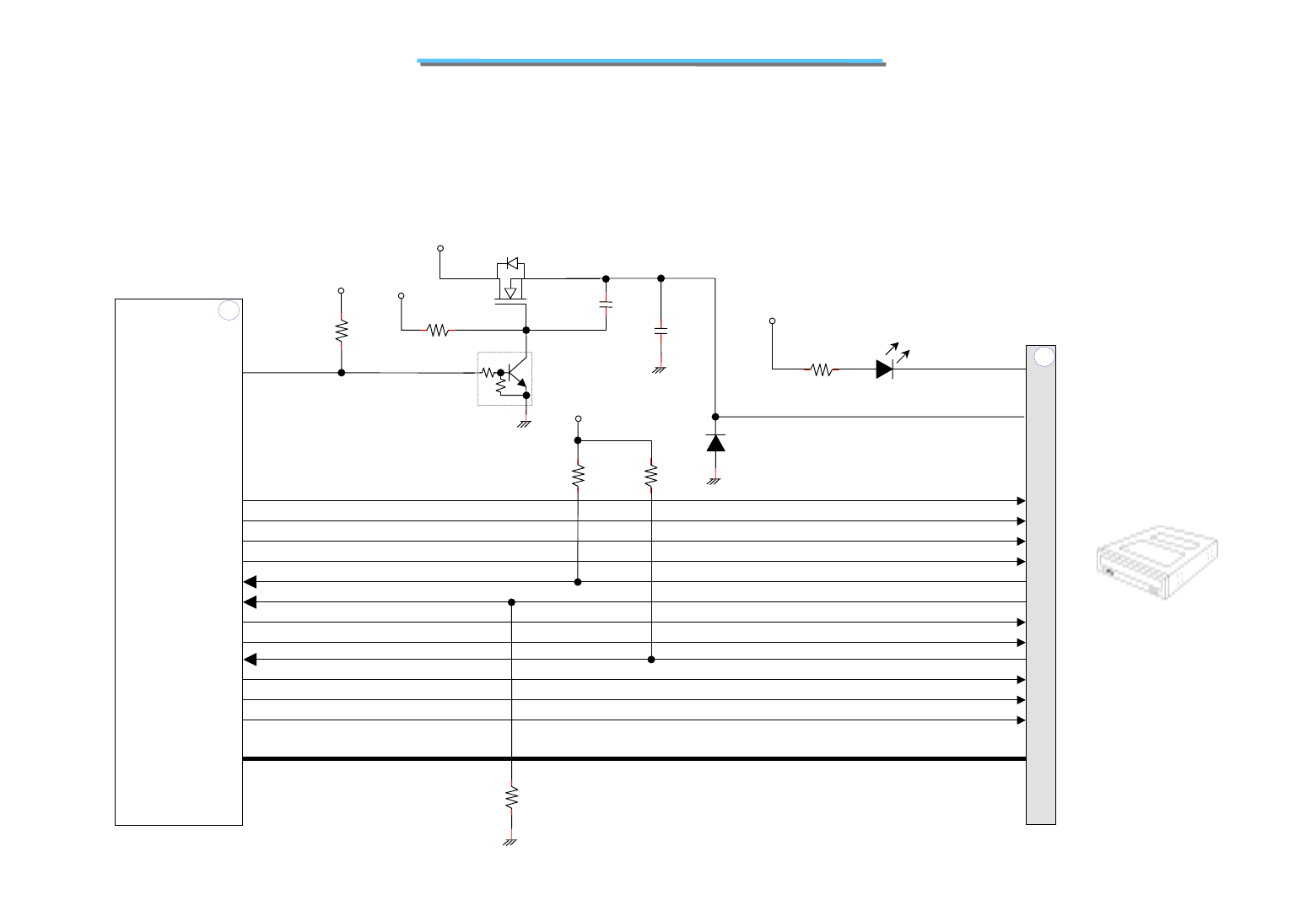
163
8170 N/B MAINTENANCE
8.9 CD-ROM Drive Test Error
An error message is shown when reading data from CD-ROM drive.
U17
ICH2
82801BA
-CDROM_RST
J10
5
+3VS
-SDACK
SDA1
SDA0
SIORDY
SDREQ
-SDIOW
-SDIOR
IRQ15
-SCS1
-SCS3
SDA2
SDD [0:15] SDD [0:15]
-SDACK
SDA1
SDA0
SIORDY
SDREQ
-SDIOW
-SDIOR
IRQ15
-SCS1
-SCS3
SDA2
+5VS
R682
470
D11
PG1102W
29
35
36
34
24
25
22
27
33
31
28
37
-CDACTP
Secondary EIDE Connector
For CD-ROM
G
DS
+12VS
R580
10K
R577 1M
-CDROM_PWRON
+5VS
Q504
DTC144WK
Q503
DTC144WK
C587
4.7U
C593
0.1U
-CDROM_RST
+5VS
R36
10K
R37
4.7K
R582
5.6K
38-42
D508
EC10QS04
P13
P14
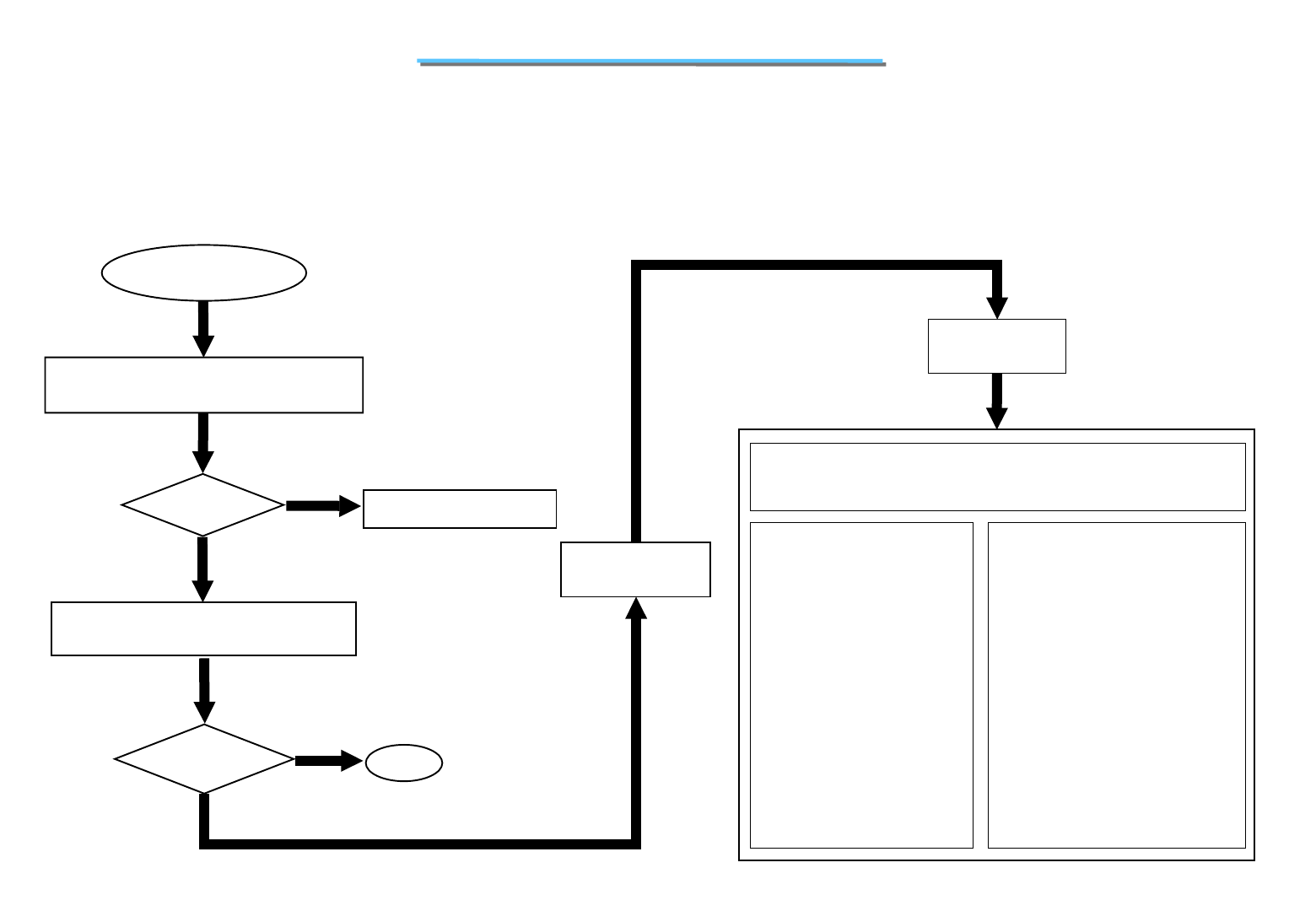
164
8170 N/B MAINTENANCE
CD-ROM Driver
Test Error
Yes
No
Test
OK? Replace the faulty parts.
1. Try another known good compact disk.
2. Check install for correctly.
Check the CD-ROM driver for proper
installation.
No
Re - Test
OK? End
Yes
Replace
Motherboard
One of the following parts or signals on the motherboard may be
defective, use an oscilloscope to check the signals or replace the parts
one at a time and test after each replacement.
PARTS: SIGNALS:
U17 R580
R577 Q503
Q504 C593
C587 R36
R37 R582
R682 D12
J10
-CDROM_RST
CDROM_PWRON
-SDACK
SDA1
SDA0
SIORDY
SDERQ
-SDIOW
-SDIOR
IRQ15
-SCS1
-SCS3
SDA2
SDD[0:15]
Board-level
Troubleshooting
8.9 CD-ROM Drive Test Error
An error message is shown when reading data from CD-ROM drive.
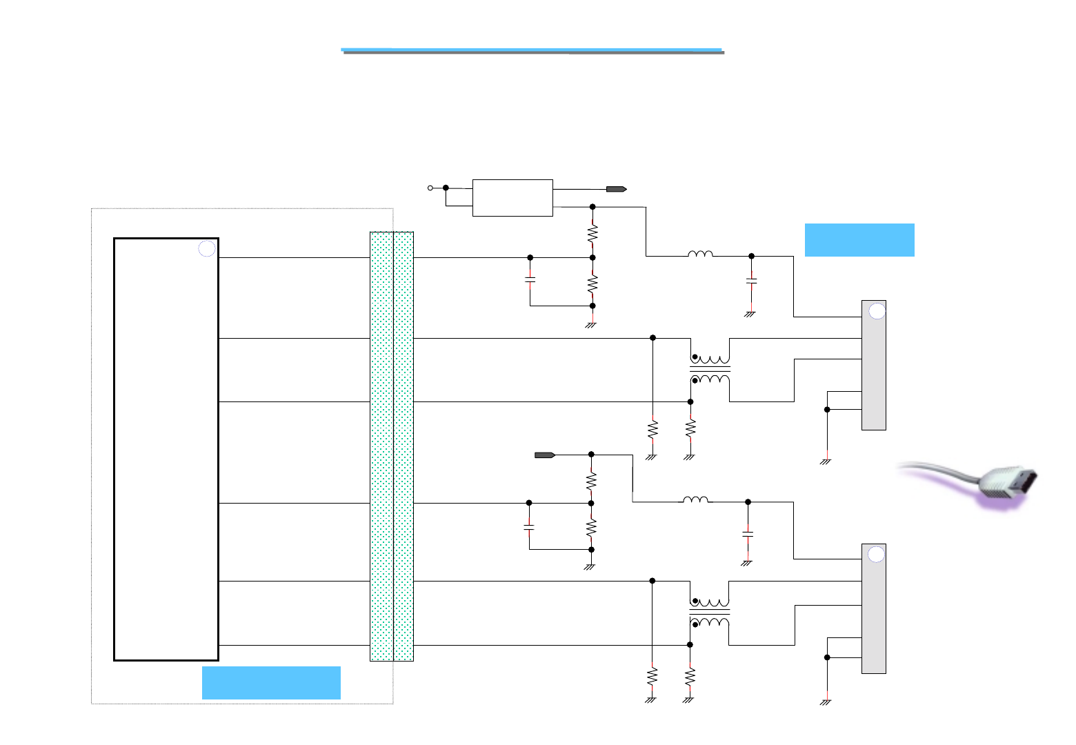
165
8170 N/B MAINTENANCE
8.10 USB Port Test Error
An error occurs when a USB I/O device is installed.
12
34
U17
ICH2
82801BA
+5V
USB2VCC5
-USBOC1
USBP2_2-
USBP2_2+
-USBOC0
USBP0_0-
USBP0_0+
J2
J6
VCCOUT1
R4
33k
R3
47k
C1
1000P
R5
33K
R6
47K
C4
1000P
L1
L4
120Z/100M
120Z/100M
C501
0.1U
L2
200Z/100M
1
2
3
4
GND
R502
15K
R503
15K
R504
15K R505
15K
C502
0.1U
1
2
3
4
GND
12
34 L3
600Z/100M
GND_USB
VCCOUT0
VIN0
VIN1
3
41
2USB0VCC5
U2
RT9701-CBL
PJ2J6
46
16
14
USB0VCC5
48
30
28
-USBOC1
USBP2_2-
USBP2_2+
-USBOC0
USBP0_0-
USBP0_0+
46
16
14
48
30
28
P13
P3
P3
Mother Board
D/D Board

166
8170 N/B MAINTENANCE
USB Test Error
Check if the USB device is installed
properly. (Including charge board.)
Re-test
OK?
No
Yes
No
Yes Correct it
Replace another known good charge
board or good USB device.
Replace
Motherboard
Correct it
Test
OK?
Check the following parts for cold solder or one of the following parts
on the mother-board may be defective, use an oscilloscope to check the
following signal or replace the parts one at a time and test after each
replacement.
Parts: Signals:
U17 J6
PJ2 U2
R4 R3
C1 C502
R[502:505]
L[1:4] R5
R6 C4
J2 J6
VCC5
USBVCC5
-USBOC1
USBP2_2-
USBP2_2+
-USBOC0
USBP0_0-
USBP0_0+
Board-level
Troubleshooting
8.10 USB Port Test Error
An error occurs when a USB I/O device is installed.
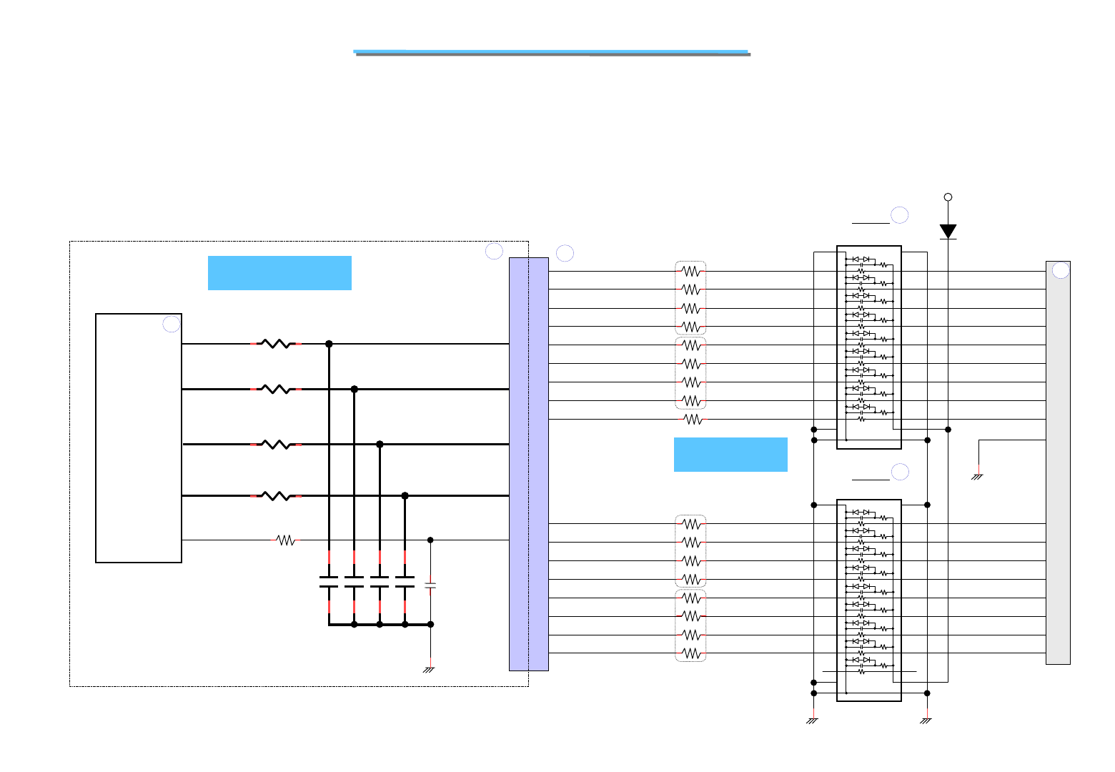
167
8170 N/B MAINTENANCE
8.11 PIO Port Test Error
When a print command is issued, printer prints nothing or garbage.
P_LPD [0:3]
P_LPD [4:7]
P_SLCT, -P_STB
-P_AFD, -P_ERR
-P_INIT, -P_SLIN
-P_ACK, P_BUSY
P_PE DP_PE
RP500
0*4
RP502
0*4
RP503
0*4
RP504
0*4
R500
0
CP502
100P*4
CP503
100P*4 CP504
100P*4 CP505
100P*4
C504
22P
Mother Board
J6
DP_LPD [0:3]
DP_LPD [4:7]
DP_SLCT, -DP_STB
-DP_AFD, -DP_ERR
-DP_INIT, -DP_SLIN
-DP_ACK, DP_BUSY
STB#
AFD#
LPD0
ERR#
LPD1
INIT#
LPD2
SLIN#
LPD3
-P_STB
-P_AFD
P_LPD0
-P_ERR
P_LPD1
-P_INIT
P_LPD2
-P_SLIN
P_LPD3
-P_ACK
P_BUSY
P_PE
P_SLCT
P_LPD4
P_LPD5
P_LPD6
P_LPD7
8
7
6
5
1
2
3
4
8
7
6
5
1
2
3
4
RP1
RP2
R1 0
8
7
6
5
1
2
3
4
8
7
6
5
1
2
3
4
RP3
120OHM/100MHZ
RP4
120OHM/100MHZ
-PP_STB
-PP_AFD
P_LPD0
-PP_ERR
PP_LPD1
-PP_INIT
PP_LPD2
-PP_SLIN
PP_LPD3
-PP_ACK
PP_BUSY
PP_PE
PP_SLCT
PP_LPD4
PP_LPD5
PP_LPD6
PP_LPD7
XX
+5VS
D501
BAS32L
Parallel Port
Connector
J1
PJ2
U501
PAC128401Q
U502
PAC128401Q
ACK#
BUSY
PE
SLCT
LPD4
LPD5
LPD6
LPD7
12
11
10
9
8
7
6
5
4
3
2
1
13
14
15
16
17
18
19
20
21
22
23
24
12
11
10
9
8
7
6
5
4
3
2
1
13
14
15
16
17
18
19
20
21
22
23
24
1
14
2
15
3
16
4
17
5
6
7
8
9
10
11
12
13
GND_IO2
18-27
GND_IO2 GND_IO2
25
23
43
21
41
19
39
17
37
35
33
31
29
36
34
32
27
U509
Supper I/O
PC87393
D/D Board
P18
P22 P2
P3
P3
P3
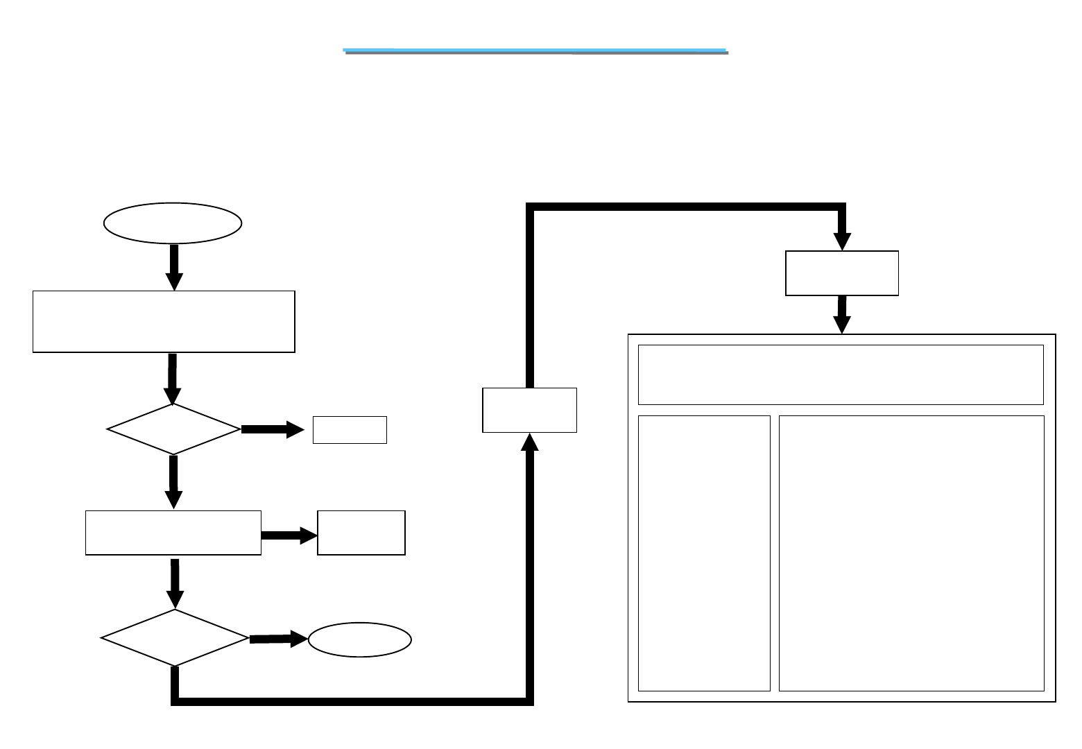
168
8170 N/B MAINTENANCE
Yes
No
Test
OK?
Replace the
faulty parts.
1. Check if PIO device is installed
properly. (J1)
2. Check CMOS LPT port setting properly.
Try another known good
PIO device.
No
Re - Test
OK? End
Yes
Correct it
Replace
Motherboard
PIO Test Error
Yes
No
One of the following parts or signals on the motherboard may be
defective, use an oscilloscope to check the signals or replace the parts
one at a time and test after each replacement.
PARTS: SIGNALS:
U509 RP500
R500 C504
J6 PJ2
RP1 RP2
R1 RP3
RP4 U501
U502 J1
RP[502:504]
CP[503:505]
P_SLCT,
-P_STB
-P_AFD,
-P_ERR
P_LPD [0:7]
-P_INIT,
-P_SLIN
-P_ACK,
P_BUSY
P_PE
AFD#
LPD0
ERR#
LPD1
INIT#
Board-level
Troubleshooting
8.11 PIO Port Test Error
When a print command is issued, printer prints nothing or garbage.
SLIN#
LPD3
LPD2
LPD4
LPD5
LPD6
LPD7
ACK#
BUSY
PE
SLCT
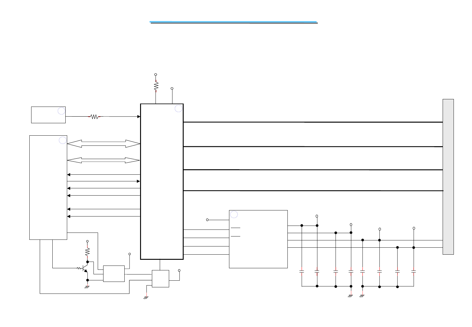
169
8170 N/B MAINTENANCE
8.12 PC-Card Socket Failure
An error occurs when a PC card device is installed.
VPPEN0
VPPEN1
-VCCEN1
-VCCEN0
C609
0.1u
C612
0.1u
C603
0.1u
C600
0.1u
C594
0.1u
C601
0.1u
C82
0.1u
C599
0.1u
+3V
+5V VCCA VPPA
3.3VA,B
5VA,B
AVCCC,B,A
AVPP
+12V
3,4
5,6
11-13
10
9
2
1
15
14
VCCD0
VCCD1
VDDP0
VDDP1
U504
TPS2211
CAD [0:31]
-CCBE [0:3]
R2_D2 R2_D14 R2_A16 CPARC
VS[1:2] CSTCHG
CCLK -CRST -CAUDIO
-CBLOCK -CCLKRUN
-CCD[ 1:2]
J8
Card Bus
Socket
PCI BUS
-CBE [0:3]
VCCA
+3V
U7
PCI4410GHK
R46
0
A21 / IDSEL
-IRQ0
-GNT0
-CARD_RI
SERIRQ
-INTA
-INTC
-CIRDY -CPERR -CSERR
-CSTOP -CTRDY -CINT
-CREQ -CGNT -CDEVSEL
U17
ICH2
82801BA
A
B
Y
4
5
3
2
1
+3V
-PCIRST_N
+3V
+3V_ICH
R158
4.7K
A
B
GNT
VCC
Y4
5
U16
1
2
3
-PCIRST
-PCIRST_RST
Q15
-GATE1394
GNT
-CBRST
U8
NC7S08
PCICLK_CARD
10 R607 33
U507
ICS950805 CAD [0:31]
-CCBE [0:3]
CCLK -CRST -CAUDIO
-CBLOCK -CCLKRUN
-CCD[ 1:2]
-CIRDY -CPERR -CSERR
-CSTOP -CTRDY -CINT
-CREQ -CGNT -CDEVSEL
R2_D2 R2_D14 R2_A16 CPARC
VS[1:2] CSTCHG
P8P15
P13
P15
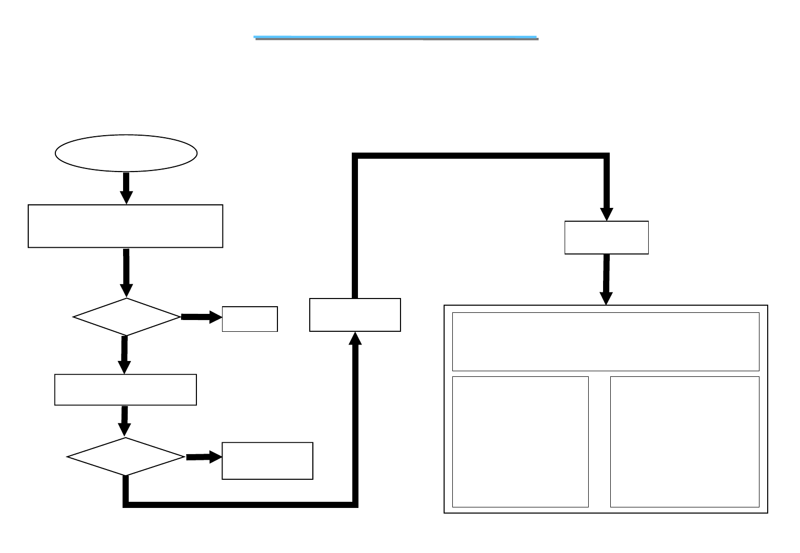
170
8170 N/B MAINTENANCE
PC Card and
Test Error
1. Check if the PC CARD device
is installed properly.
2. Confirm PC card driver is installed ok.
Test
OK?
Re-test
OK?
Yes
No
Yes
No
Change the faulty
part then end.
Try another known good
PC card device.
Correct it
Replace
Motherboard Check the following parts for cold solder or one of the following
parts on the mother-board may be defective, use an oscilloscope
to check the following signal or replace the parts one at a time and
test after each replacement.
Parts: Signals
R607 U507
U17 U8
U7 U9
C82 J8
C594 C599
C600 C602
C603 C609
PCI BUS SIGNAL
CCLK -CRST
-CAUDIO -CBLOCK
-CCLKRUN -CCD[ 1:2]
R2_D2 R2_D14
R2_A16 CPARC
VS[1:2] CSTCHG
-VCCEN1 -VCCEN0
VPPEN0 VPPEN1
Board-level
Troubleshooting
8.12 PC-Card Socket Failure
An error occurs when a PC card device is installed.
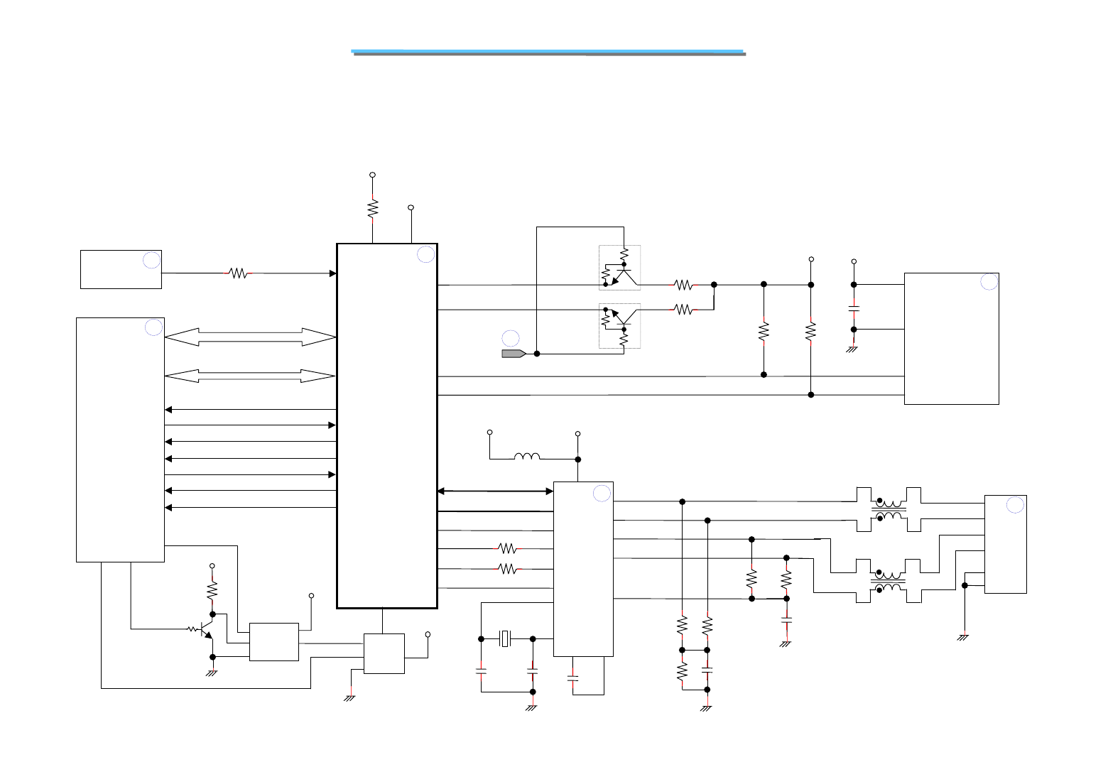
171
8170 N/B MAINTENANCE
8.13 IEEE1394 Failure
An error occurs when a PC card device or 1394 device is installed.
PCI BUS
-CBE [0:3]
VCCA
+3V
U7
PCI4410GHK
R46
0
A21 / IDSEL
-IRQ0
-GNT0
-CARD_RI
SERIRQ
-PCLKRUN
-INTA
-INTC
U17
ICH2
82801BA
A
B
Y
4
5
3
2
1
+3V
-PCIRST_N
+3V
+3V_ICH
R158
4.7K
A
B
GNT
VCC
Y4
5
U16
1
2
3
-PCIRST
-PCIRST_MSK
Q15 -GATE1394
GNT
-CBRST
U8
NC7S08
PCICLK_CARD
10 R607 33 Q5
DTC144WK
Q4
DTC144WK
R43
47K
R42
47K
+3V
R53
4.7K
R52
4.7K
C99
0.1U
+5V
U9
NM24C02N
Write Protect
when high
8
7
VCC
WC-
SDA
SCLK
5
6
-1394WR
VCCEN1
VCCEN0
PHY_D [0:7]
PHY_CTL[0:1]
PHY_LREQ
PHY_CLK
PHY_LKON
PHY_LPS
+3V 1394AVDD
1
2
19
15
R73 10
R80 10
C152
10P
C134
10P
X504
24.576MHZ
12
60
59
TPB-
TPB+
35
30,31,42
34
R106
56
R124
4.99K
R105
56
C199
270P
TPA-
TPA+
36
37
R103
56
R115
56
L20
L24
PLP32166
PLP32166
L23
1
12
43
12
432
3
4
GND1
GND2
J21
U14
TSB41AB1
C200
1U
38
C161
0.1U
54 55
TPBIAS
FILTER0
FILTER1
NC7S32
U507
ICS950805
P8
P13
P15
P13
P15
P15
P15
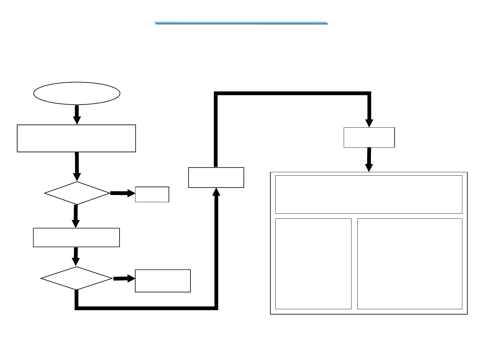
172
8170 N/B MAINTENANCE
IEEE1394 Test Error
1. Check if the 1394 device is installed
properly.
2. Confirm 1394 driver is installed ok.
Test
OK?
Re-test
OK?
Yes
No
Yes
No
Change the faulty
part then end.
Try another known good
1394 device.
Correct it
Replace
Motherboard Check the following parts for cold solder or one of the following
parts on the mother-board may be defective, use an oscilloscope
to check the following signal or replace the parts one at a time and
test after each replacement.
Parts: Signals
PCI BUS SIGNAL
PCICLK_CARD
-CBE[0:3] -IRQ0
-GNT0 -CARD_RI
SERIRQ -INTA
-INTC CBRST
VCCEN0 VCCEN1
PHY_D[0:7]
PHY_CTL[0:1]
PHY_LREQ
PHY_CLK
PHY_LKON
PHY_LPS
TPA+
TPA-
TPB+
TPB-
PHY_XI
PHY_XO
U507 U17 U7
U8 U14 X504
C134 C152 Q5
Q4 R43 R42
R53 R52 U9
C99 L23 L24
J21 R105 R103
R115 R106 R124
C199 C200 R607
Board-level
Troubleshooting
8.13 IEEE1394 Failure
An error occurs when a PC card device or 1394 device is installed.
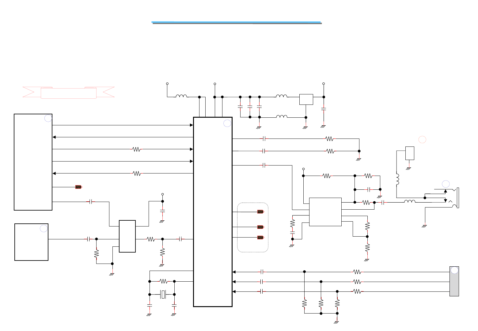
173
8170 N/B MAINTENANCE
8.14 Audio Failure
No sound from speaker after audio driver is installed.
U17
ICH2
82801BA U15
ALC201
U7
PCI4410
C670
0.1U
C667
0.1U
+3VS
C702
0.1U
C684
10U C674
0.1U
L540
SBSPKR
R649
47K
+5VS
R646
470K R647
20K
U510
NC7S32
R645 22
R648 22
-CARDSPK
11
5
8
10
6
12
1 9 25 38
1
2
3
5
4
62
AVDDAD
PC_BEEP
L14
120Z/100M
C672
0.1U
R109 6.8K
R121 6.8K
AGND
23
24
LINE/IN/L
LINE/IN/R
5
4
3
2
1
X
CAGND
J22
External
Micro Phone
Jack
J16
Internal
Micro Phone
Jack
2
21
MIC1
XTL/IN
XTL/OUT
A
B
GND
VCC
Y
C669
0.1U
CD-ROM
Audio Jack
R141
0
R142
6.8k
J10
20
18
19
2
1
3
R140
6.8k
CD/R
CD/L
CD/GND
P17
SPK_OFF To U18
Next Page
36
35
LINE/OUT/R
LINE/OUT/L To next
Page
AGND
MIC1
MIC_3
2
1
IO
GND
+12VS
13
2
U511
7805
C196 2.2U
C183 2.2U
C194 1U
-ACRST
ACSDOUT
ACSDIN
ACSYNC
ACBITCLK
L535
120Z/100M
L525
120Z/100M
C701
0.068U/25V
VCC+
2OUT
8
AVDDAD
R669 47K R670 47K
C686 10U/10V
3
1
2
1OUT
1IN+
2IN+ R148
68K
R149
100K
2IN-
7
6
4
AOUT_R
AOUT_L
R151
100K
C209
10U/10V
CDROM_RIGHT
CDROM_LEFT
CDROM_COMM
R134 6.8K
R132 6.8K
R133 0
C193 1U
C191 1U
C192 1U
U513
MC33078D
C675
0.1U
3
R88 1M
X2 24.576M
C148
10P
C167
10P
AUDIO IN
48 SPDIFOUT
MIC_2
L522
P13
P17
VCC-
R671 4.7K
5
2IN+
P15
P14
P17
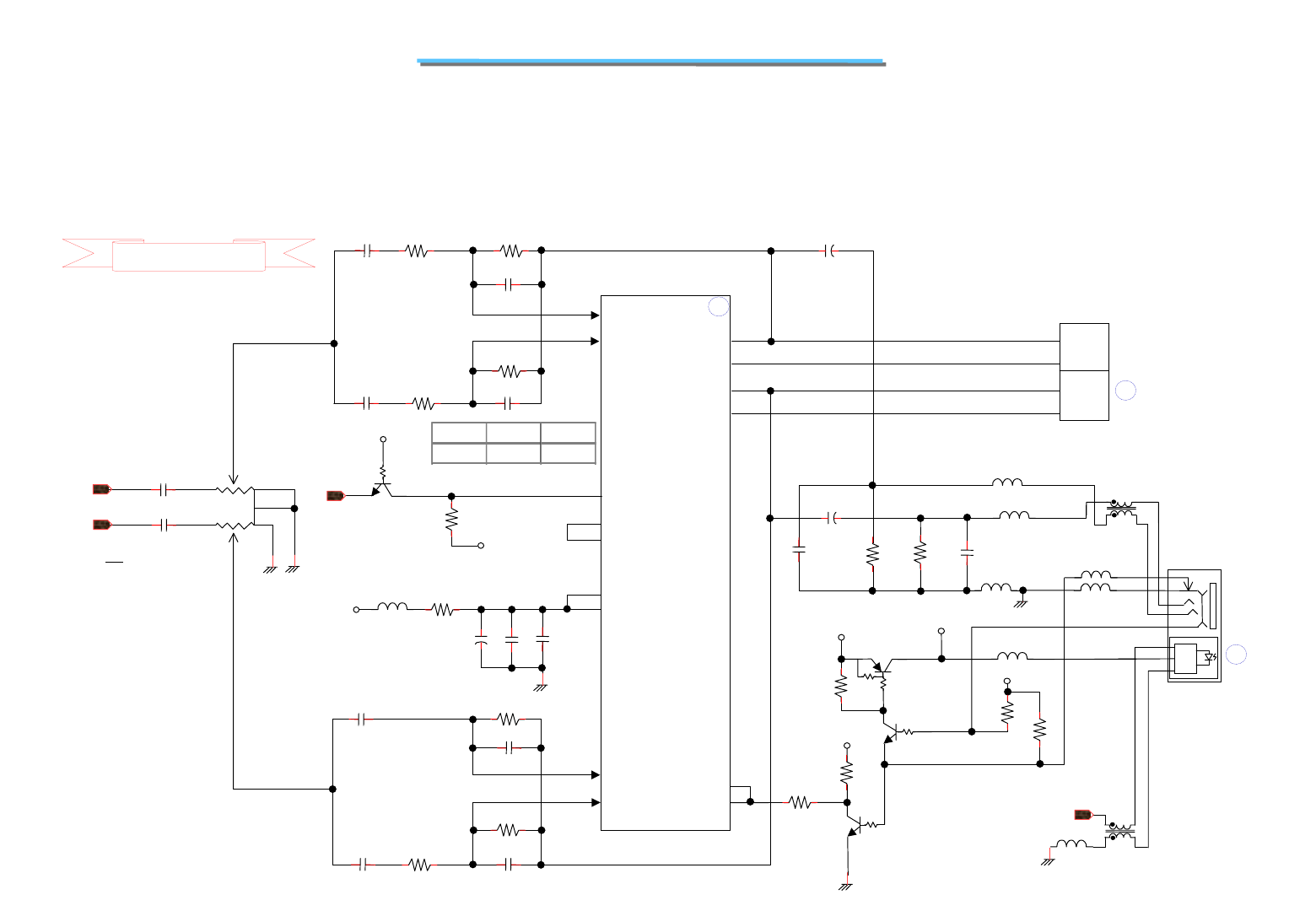
174
8170 N/B MAINTENANCE
1
2
3
6
5
47
AOUT_R
AOUT_L
VR1
10K
From U15
front page
C710 2.2U
C709 2.2U
R678 10K
R677 10K C693 470P
R667 15K
C694 680P
C708 2.2u
C707 2.2u
R676 10k
R675 10k C691 470P
R665 15k
C692 680P
SPK_OFF
5
4
2
3
1
C210 220U
C166
100U
C206
0.1U
C168
0.1U
U18
Amplifier
TPA0202
RLINE IN
RHP IN
21
20
LLINE IN
LHP IN
4
5
18
7RVDD
LVDD
11 MUTE IN
MUTE OUT
SHUTDOWN
9
8
R548 22
L47
120Z/100M
5V_AMP
From U17
R143
1K
SPKROUT+
SPKROUT-
SPKLOUT+
SPKLOUT-
R OUT+
R OUT-
L OUT+
L OUT-
22
15
3
10
SE/BTL#
HP/LINE#
14
16
1
2
1
2
R
L
J19
Line Out
Phone Jack
J20
J18
Internal
Speaker
Connector
AUDIO OUT
R666 10K
R664 10K
7
8
9
21
34
L536
PLP3216S
L524 120Z/100M
C689
100P
C204 220U
R122
1K C688
100P
L529 120Z/100M
L523 120Z/100M
+3VS_SPD
+3VS Q514
DTA144WK
5V_AMP
R673
4.7K
R685
10K
-DECT_HP/OPT
Q515
DTA144TKA
Q10
DTA144TKA
5V_AMP R659
4.7K
R102
47K
R113
100K
Signal HI LOW
SPK_OFF Shut Down Normal
-DEVICE_DECT
L532
PLP3216S
21
34
From U15
front page
SPDIFOUT
L527
120Z/100M
L537
L538
120Z/100M
L531 120Z/100M
LINE_OUT_5
LINE_OUT_2
C717 4.7U
C718 4.7U
+3V_ICH
Q16
DTC144TKA
+5VS
R166
10K
P17
P17
P17
8.14 Audio Failure
No sound from speaker after audio driver is installed.
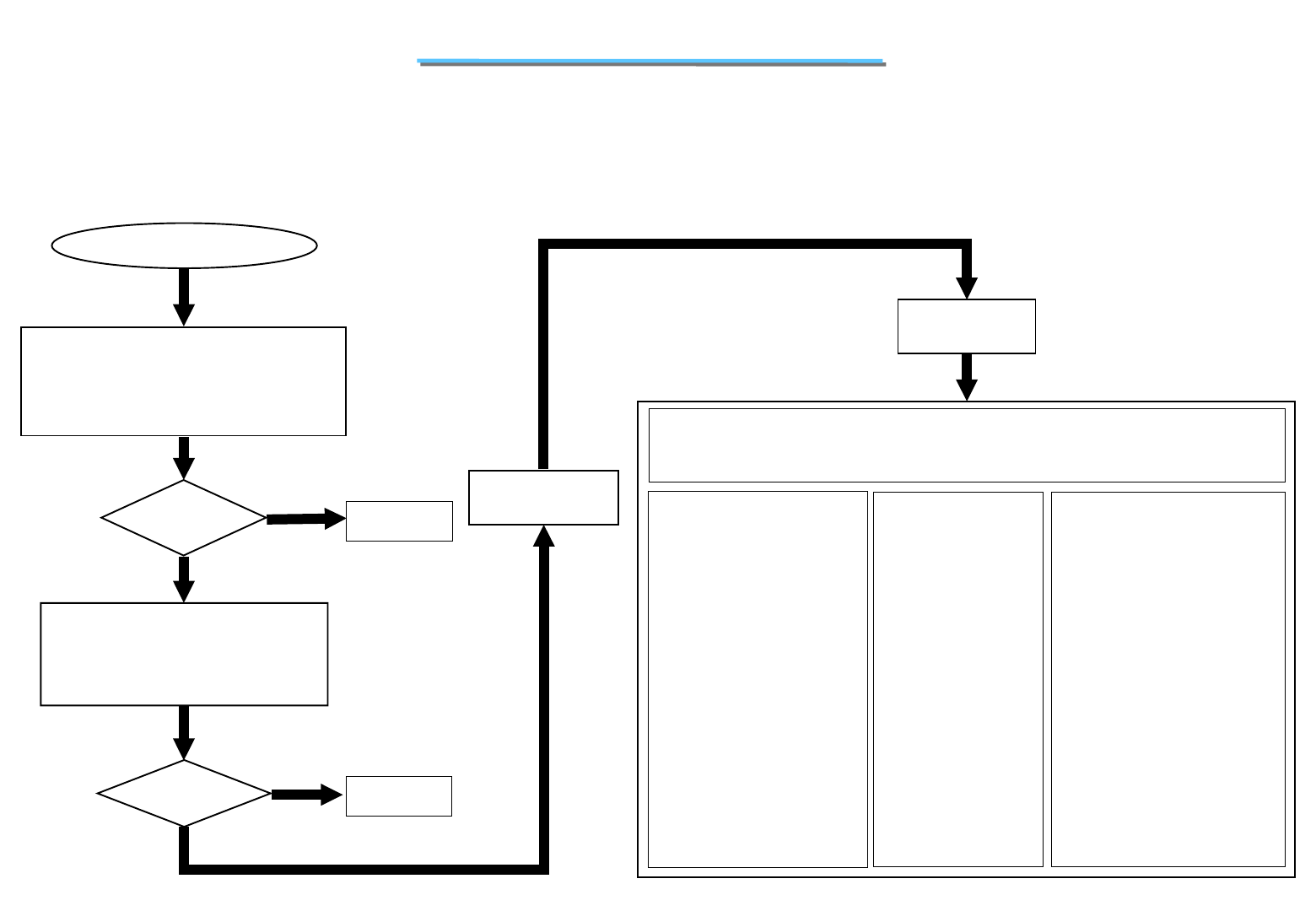
175
8170 N/B MAINTENANCE
Test
OK?
Audio Drive Failure
1. Check if speaker cables are connected
properly.
2. Make sure all the drivers are installed
properly.
1.Try another known good speaker,
CD-ROM.
2. Exchange another known good
charger board.
Re-test
OK?
Replace
Motherboard
Yes
Correct it.
Correct it.
Yes
Check the following parts for cold solder or one of the following parts on the
motherboard may be defective,use an oscilloscope to check the following signal
or replace parts one at a time and test after each replacement.
Signals:
AOUT_R
AOUT_L
SPKROUT+
SPKROUT-
SPKLOUT+
SPKLOUT-
LINE_OUT_5
LINE_OUT_2
SPK_OFF
SPDIFOUT
1.If no sound cause
of line out, check
the following
parts & signals:
2. If no sound cause
of MIC, check
the following
parts & signals:
3. If no sound cause
of CD-ROM, check
the following
parts & signals:
Parts: Signals:
MIC
MIC_2
MIC_3
Parts: Signals:
CDROM_RIGHT
CDROM_LEFT
CDROM_COMM
Parts:
No
No
J10
R[132:134]
R[140:142]
C[191:193]
J16 J22 U15
L535 L525
C701 R148
R149 R669
U513 C194
R151 C209
R670 C686
U15 X2
U510 U507
U17 U511
VR1 U18
C[707:710]
R[664:667]
C[691:694]
L47 Q514
Q515 Q10
L[537:539]
L523 L524
L528 L531
J[18:20]
Board-level
Troubleshooting
8.14 Audio Failure
No sound from speaker after audio driver is installed.
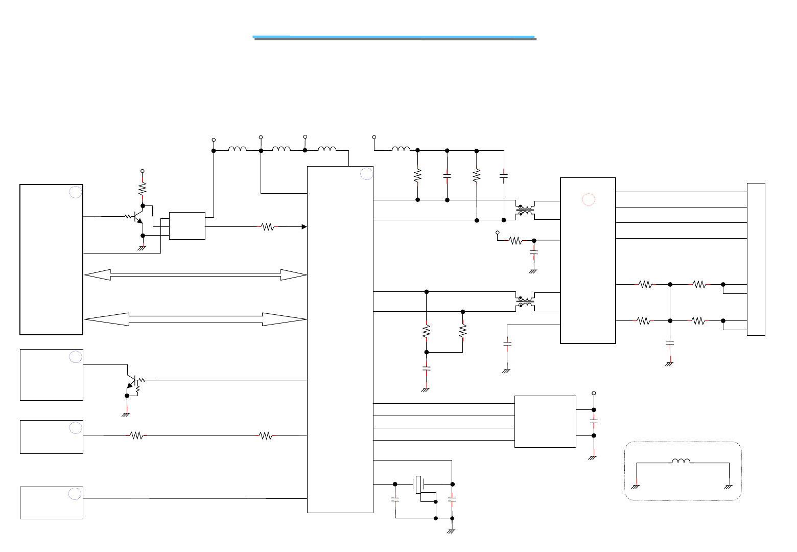
176
8170 N/B MAINTENANCE
An error occurs when a LAN device is installed.
8.15 LAN Test Error
TX+
TX-
RX+
RX-
10
9
16
15
TXC
RXC
11
14
U2
2
1
5
4
8
7
6
3
J9
RJ45
U4
LANPHY
RTL8139CL
U17
ICH2
82801BA
P17
-DEVSEL,-STOP,-PCI_INTD
+3V
+3V_ICH
R158
4.7K
A
B
GNT
VCC
Y4
5
U16
1
2
3
-PCIRST
-PCIRST_MSK
Q15
NC7S32
R31 0
115
U508
H8
F3437
Q512
DTC144WK
3
2
1
48
83
LAN_WAKE
U507
ICS950805
116
PCICLK_LAN
R610 33
11
-CBE[0:3]
AD[0:31],-PCI_REQ1,-PCI_GNT1
-PCI_IRDY,-PCI_TRDY,-FRAME
L12
120Z/100M +3V_LAN
L10 L9
AVDD_LAN
RXIN-
RXIN+
86
87
R549
51
R555
51
C577
0.1U
21
34
1
2
RD+
RD-
RDC
L513
PLP3216A
TXD+
TXD-
7
8
TD+
TD-
92
91
21
34
EECS
MA2
MA0
MA1
1
2
3
4
C69
0.1u
8
5
CS
SK
DI
DO
VCC
GND
U5
93C468
3V_LAN
50
49
48
47
XTALOUT
X501
25MHZ
3
2
4
1
C585
10P
C584
10P
79
78
XTALIN
3
C40
0.1U
6
C567
22P
L508
PLP3216A
R541
51
C572
22P
R542
51 PJTX+
PJTX-
PJRX+
PJRX-
R12 75
R17 75
R530 75
R531 75
C566
1000P
PJ4
PJ7
U7
PC14410GHK
75
R32 0
-PCLKRUN
L8
PLP3216A
L_AGND
H0011
XFMR_H0009
-PCIRST_N
77,90,96
AVDD_LAN
L511
P16
AVDD_LAN R15 0
C39
0.1U
P13
P19
P15
P8

177
8170 N/B MAINTENANCE
LAN Test Error
Yes
No
Test
OK? Correct it.
Correct it.
No
Check if BIOS setup is ok.
Re-test
OK?
Replace
Motherboard
1.Check if the driver is installed properly.
2.Check if the notebook connect with the
LAN properly.
Yes
Check the following parts for cold solder or one of the following
parts on the mother-board may be defective, use an oscilloscope
to check the following signal or replace the parts one at a time and
test after each replacement.
Parts: Signals
TXD+
TXD-
PJTX+
PJTX-
PJRX+
PJRX-
PJ4
PJ7
-PCIRST_N
-CBE[0:3]
LAN_WAKE
PCICLK_LAN
PCLKRUN
XTALIN
XTLOUT
RXIN-
RXIN+
U17 U508 U507
R158 U16 Q512
R610 R32 R31
U4 L[8:10] R542
R541 R549 R555
L508 L513 C567
C572 C577 C540
U5 C69 X501
C584 C585 R12
R17 R530 R31
J9
Board-level
Troubleshooting
An error occurs when a LAN device is installed.
8.15 LAN Test Error
178
8170 N/B MAINTENANCE
9. Spare Parts List -- recommend (1)
Category Part Number Description Remark
CPU 324180786162 BFM-IPC;IC,CPU,WILLA 526267120029(1/15 Delete,
The CPU not use in the part
SDRAM MODUL
E
323767120001 BFM-IPC;DRAM MODULE, 526267120029
340671200007 COVER ASSY; SPEAKER,8170
340671200007 COVER ASSY;KB,8170
442164900010 TOUCH PAD MODULE;TM41PD-350
422665400002 FFC ASSY;TOUCH PAD,CASE KIT,VENU
340671200002 COVER ASSY;8170
340671200006 COVER ASSY;RAM,8170 1/17 ECR:7939102700 delet
e
340671200025 COVER ASSY;RAM-1,8170 1/17 ECR:7939102700 add
343671200003 PLATE;KEYBOARD,8170
344669900003 COVER;HINGE,7170
421669900007 WIRE ASSY;TOUCHPAD,7170
340671200008 BRACKET ASSY;T-P,8170
340671200019 SPERKER ASSY;L,8170
340671200012 SPEAKER ASSY;R,8170
421671200031 MICROPHONE ASSY;8170
421671200008 WIRE ASSY;MDC,8170
340671200020 FAN ASSY;8170
411671200001 PWA;PWA-8170,MOTHER BD
412155600047 PCB ASSY;MDM,56K,UNIV,F-PACK,WO/
340671200003 HOUSING ASSY;8170
BATT ASSY 442671200001 BATT ASSY;11.1V/6AH,LI-,PANASONI
COVER ASSY
PCB;PWA-8170
TOUCHPAD BD
HOUSING KIT
PWA;PWA-
8170,MOTHER
BD,T/U
Category Part Number Description Remark
411671200004 PWA;PWA-8170,D/D BD,SMT
346671200011 INSULATOR;CD-ROM,M-B,8170
346671200036 INSULATOR,MDC,8170
413000020305 BFM-IPC;LCD,UB141X01 526267120014,17,29
413000020281 LCD;14X13-102,TFT,14 526267120037
421671200002 WIRE ASSY;UNIPAC,14. 526267120014,17,29
421671200001 WIRE ASSY;HYUNDAI,14 526267120037
421671200007 WIRE ASSY;INVERTER,8170
340669900001 TILT UNIT;R,7170
340669900002 TILT UNIT;L,7170
340671200016 HOUSING ASSY;HANNSTER,14.1",LCD,
340671200017 HOUSING ASSY;UNIPAC, 526267120014,17,29
340671200015 HOUSING ASSY;HYUNDAI 526267120037
341669900004 BRACKET;LCD,14.1",HYUNDAI,L,7170
345669900004 RUBBER;LCD,DOWN,7170
345671200001 RUBBER;LCD,UP,8170
346664900010 FILM;LCD PROTEC,.14.2",235*300,5
340671200018 COVER ASSY;LCD,8170
341669900003 BRACKET;LCD,14.1,HYU
412671200001 PCB ASSY;INVERTER BD,11P,8170,MS 1/22 add option(7939102656
)
412671300001 PCB ASSY;D/A BD,SUMIDA,STINGRAY 1/22 add option(7939102656
)
PWA;PWA- 411671200007 PWA;PWA-8170,ESB BD
AC ADPT ASSY 442671200004 AC ADPT ASSY;19V/4.74A,DELTA,817
242670800113 BFM-WORLD MARK;WINXP,7521N
PWA;PWA-
8170,D/D
BD,T/U
LCD ASSY
179
8170 N/B MAINTENANCE
Category Part Number Description Remark
344669900010 CASE;HDD,7170
523467120012 BFM-IPC;HDD DRIVE,30 526267120029
531066990001 KBD;86,US,K000918E1,7170
531020237308 KBD;87,FR,K000918F1, 526267120014
531020237307 KBD;87,GR,K000918F1, 526267120017,29
332810000033 PWR CORD;125V/7A,2P,BLACK,AMERIC
332810000034 PWR CORD;250V/2.5A,2 526267120017
332810000043 PWR CORD;250V/3A,2P, 526267120037
421015560001 CABLE ASSY;PHONE LINE,6P2C,W/Z C
340669900046 BEZEL ASSY;DVD ROM,QUANTA,7170
343669900006 BRACKET;CD-ROM,7170
523430061901 DVD DRIVE;8X,SDR-081,H=12.7,QUAN
BEZEL
ASSY;DVD
ROM,QUANTA,
HDD ASSY;30G
KBD
AK;01-EN
9. Spare Parts List -- recommend (2)
180
8170 N/B MAINTENANCE
9. Spare Parts List -- All (1)
Part Number Description Location(s)
441999900204 AC ADPT ASSY OPTION;8170
442671200004 AC ADPT ASSY;19V/4.74A,DELTA,817
541667120001 AK;01-EN,BOX,8170
541667120032 AK;EN,8170,UTILITY ONLY
441999900056 BATT ASSY OPTION;LI,9-CELL,8170
442671200001 BATT ASSY;11.1V/6AH,LI-,PANASONI
298000000002 BATTERY HOLDER;FOR CR2032,BH-800 BT1
338530010018 BATTERY; LI,3V/220MAH,CR-2032 BT1
340669900046 BEZEL ASSY;DVD ROM,QUANTA,7170
242670800113 BFM-WORLD MARK;WINXP,7521N
221669940001 BOX;AK,7170
340671200008 BRACKET ASSY;T-P,8170
343669900006 BRACKET;CD-ROM,7170
341669900005 BRACKET;LCD,14.1",HANNSTAR,R,717
341669900004 BRACKET;LCD,14.1",HYUNDAI,L,7170
421015560001 CABLE ASSY;PHONE LINE,6P2C,W/Z C
421671000001 CABLE ASSY;USB FDD
272075103702 CAP;.01U ,50V,+80-20%,0603,SMT C562,C576,C60,PC32,PC500
,
272072473402 CAP;.047U,16V ,10%,0603,X7R,SMT C651
272075104701 CAP;.1U ,50V,+80-20%,0603,SMT C103,C104,C105,C109,C110,
272075104701 CAP;.1U ,50V,+80-20%,0603,SMT C501,C502,C507,C512,C513,
272003683401 CAP;0.068U,CR,25V,10%,0805,X7R C701
272075102701 CAP;1000P,50V ,+/-20%,0603,X7R,S C1,C132,C141,C173,C174,C
5
272075102701 CAP;1000P,50V ,+/-20%,0603,X7R,S C1,C4,PC18,PC517,PC518
272030102405 CAP;1000P,CR,3KV,10%,1808,X7R,TU C500,C502,C566
Part Number Description Location(s)
272075101701 CAP;100P ,50V ,+ -10%,0603,NPO,S C688,C689,PC528
272075101701 CAP;100P ,50V ,+ -10%,0603,NPO,S C503,C504,C505,C506
272431105901 CAP;100U ,10V ,20%,7343,SMT PC1,PC3,PC8
272431107509 CAP;100U,2V,20%,7343,SDK-CAP C12,C28,PC572,PC573,PC57
272075100701 CAP;10P ,50V ,+-10%,0603,NPO,SM C101,C107,C108,C117,C134,
272011106701 CAP;10U ,10V,+80-20%,1206,Y5V,S C10,C11,C13,C14,C15,C17,C
272023106701 CAP;10U ,25V ,+80-20%,1210,Y5U, PC20,PC28,PC541,PC544
272075120301 CAP;12P ,CR,50V ,5% ,0603,NPO,S C211,C212
272073180401 CAP;18P ,CR,25V ,10%,0603,NPO,S C556,C559
272071105701 CAP;1U ,CR,10V ,80-20%,0603,Y5 C122,C142,C160,C163,C164,
272071105701 CAP;1U ,CR,10V ,80-20%,0603,Y5 PC2
272003105701 CAP;1U ,CR,25V ,+80%-20%,0805, C171,C522,C545,C681,PC51
8
272003105701 CAP;1U ,CR,25V ,+80%-20%,0805, PC505
272002225701 CAP;2.2U ,CR,16V ,+80-20%,0805,Y C183,C196,C622,C625,C646,
272012225702 CAP;2.2U ,CR,16V ,+80-20%,1206,Y C638,C65,C81
272075222701 CAP;2200P,50V ,+/-20%,0603,X7R,S C531
272075221302 CAP;220P ,50V ,5% ,0603,NPO,SMT C523,C524,C546,C547,C704
272075220701 CAP;22P ,50V ,+ -10%,0603,NPO,S C187,C197,C203,C205,C504,
272021226701 CAP;22U ,10V,+80-20%,1210,Y5V,S C16,C49,C514,C552,C59,C6
1
272043226501 CAP;22U ,25V ,+-20%,1812,Y5U,SMT PC505,PC506,PC507,PC513,
272075271401 CAP;270P ,50V,+-10%,0603,X7R,SMT C199,C46,C93
272431337506 CAP;330U,4V,20%,7343,SMT PC7
272432336506 CAP;33U,16V,+-20%,7343,POSCAP,SM C30,C31
272421336501 CAP;33U,TT,8V,20%,3528,SMT C570,C571
272001475701 CAP;4.7U ,CR,10V ,+80-20%,0805,Y C125,C131,C153,C208,C35,
C
181
8170 N/B MAINTENANCE
9. Spare Parts List -- All (2)
Part Number Description Location(s)
272012475701 CAP;4.7U ,CR,16V ,+80-20%,1206,Y C182,C54,C587
272012475701 CAP;4.7U ,CR,16V ,+80-20%,1206,Y PC501,PC511,PC514
272075471401 CAP;470P ,50V,10%,0603,X7R,SMT C611,C691,C692,C693,C694,
272075471401 CAP;470P ,50V,10%,0603,X7R,SMT PC20
272075470701 CAP;47P ,50V ,+ -10%,0603,NPO,S C136,C139,C143,C149,C680,
272075509801 CAP;5P ,CR,50V,+ -.5PF,0603,NP C617,C618
272075680302 CAP;68P ,50V ,5% ,0603,NPO,SMT C630,C633
221668950010 CARD BOARD,BTM,PALLET,M722
221669950008 CARD BOARD;FRAME,PALLET,7170
221669950006 CARD BOARD;TOP,PALLET,7170
221671220002 CARTON;NON-BRAND,MSL,8170
431671200001 CASE KIT;8170
344669900010 CASE;HDD,7170
451669900051 CD ROM ME KIT;24X,7170
273000500052 CHOKE COIL;0.7UH,1.6mOHM,25%,20A PL1,PL2
273000500053 CHOKE COIL;10UH,21.6mOHM,5.4A PL7
273000500053 CHOKE COIL;10UH,21.6mOHM,5.4A PL1
273000111004 CHOKE COIL;160OHM/100MHZ,25%,321 L23,L24,L508,L513,L532,L5
3
273000111004 CHOKE COIL;160OHM/100MHZ,25%,321 L2,L3
273000500015 CHOKE COIL;50UH(REF),D.4*2,5.5T, L1
331000007009 CON;BAT,7P,2.5MM,CENLINK J28
331720015006 CON;D,FM,15P,2.29,R/A,3ROW J1
331720025005 CON;D,FM,25P,2.775,R/A J1
291000153006 CON;FPC/FFC,15P*2,.8MM,BD/BD,ST, J11
291000144004 CON;FPC/FFC,20P*2,1.0MM,H=4.6,ST J2
Part Number Description Location(s)
291000142404 CON;FPC/FFC,24P,1MM,H8.2,ST,ACES J12
291000150804 CON;FPC/FFC,8P,1MM,R/A,2CONTAC,E J500
331040020004 CON;HDR,FM,10P*2,2.54MM,R/A,H8,4 J3
331030044013 CON;HDR,FM,22*2,2MM,ST,C16805
331040050011 CON;HDR,FM,25P*2,1.27MM,R/A,HSG J6
291000011024 CON;HDR,FM,5P*2,1.27MM,ST,H4.5,S J501
331040020005 CON;HDR,MA,10P*2,2.54MM,R/A,H8.4 PJ1
291000011209 CON;HDR,MA,12P*1,1.25,ST,SMT J6
291000024409 CON;HDR,MA,22P*2,2MM,R/A,SMT,ALL J14
331040050009 CON;HDR,MA,25P*2,1.27MM,R/A,HSG PJ2
331040050010 CON;HDR,MA,50P,0.8MM,R/A,H1.1 J10
291000011027 CON;HDR,MA,5P*2,1.27MM,ST,H17.5, J5
291000020303 CON;HDR,SHROUD,MA,3P,1.25MM,R/A, J502
291000256823 CON;IC CARD PART;68P,0.635,H5,SM J8
331000004018 CON;IEEE1394,MA,4P,.8MM,R/A,LINK J21
331870004017 CON;MINI DIN,4P,R/A,W/GROND,C108 J4
331810006044 CON;PHONE JACK,6P2C,H11.5,RJ11,T J13
291000810806 CON;PHONE JACK,8P8C,SMD,RJ45 J9
331840010005 CON;POF MINI JACK,10P,W/SPDIF,2F J19
331910003039 CON;POWER JACK,3P,D=2.0,SINGATRO J5
331840005013 CON;STEREO JACK,5P,R/A,28MF60-07 J22
331000004025 CON;USB,MA,R/A,4P*1,2MM,85116-40 J2,J3
291000410201 CON;WFR,MA,2P,1.25,ST,SMT/MB J16,J18,J20,J4
291000410301 CON;WFR,MA,3P,1.25,ST,SMT/MB J7
291000410401 CON;WFR,MA,4P,1.25MM,ST,SMT J501

182
8170 N/B MAINTENANCE
9. Spare Parts List -- All (3)
Part Number Description Location(s)
291000410401 CON;WFR,MA,4P,1.25MM,ST,SMT J15
345669600065 CONDUCTIVE TAPE;MB,SDRAM,RACE
340671200007 COVER ASSY; SPEAKER,8170
340671200002 COVER ASSY;8170
340671200001 COVER ASSY;ID1,8170
340671200009 COVER ASSY;KB,8170
340671200018 COVER ASSY;LCD,8170
340671200006 COVER ASSY;RAM,8170
344671000001 COVER;FOR 7170;USB FDD
344669900003 COVER;HINGE,7170
272625220401 CP;22P*4 ,8P,50V ,10%,1206,NPO,S CP500,CP501,CP502,CP503,
291006214438 DIMM SOCKET;144P,.8MM,H4,SX6E,HR J505
291006214439 DIMM SOCKET;144P,.8MM,H4,SX6ER,H J503
288100032013 DIODE;BAS32L,VRRM75V,MELF,SOD-80 PD503
288100032013 DIODE;BAS32L,VRRM75V,MELF,SOD-80 D501
288100054001 DIODE;BAT54,30V,200mA,SOT-23 D10,D16
288100701002 DIODE;BAV70LT1,70V,225MW,SOT-23 D509,D510
288100701002 DIODE;BAV70LT1,70V,225MW,SOT-23 PD2,PD3
288100099001 DIODE;BAV99,70V,450MA,SOT-23 D1,D3,D4,D6
288100099001 DIODE;BAV99,70V,450MA,SOT-23 D501,D502,D503,D504,D50
5
288100099001 DIODE;BAV99,70V,450MA,SOT-23 D502,D503
288100056003 DIODE;BAW56,70V,215MA,SOT-23 PD500,PD502
288100056003 DIODE;BAW56,70V,215MA,SOT-23 PD502
288101003001 DIODE;EC10QS03L,30V,1A,SMT D508,D513
288101003001 DIODE;EC10QS03L,30V,1A,SMT PD503,PD504
Part Number Description Location(s)
288100112003 DIODE;EC11FS2-TE12L,SCHOTTKY,200 D500
288100112003 DIODE;EC11FS2-TE12L,SCHOTTKY,200 PD1
288103103001 DIODE;EC31QS03L,30V,3A,SMT PD1,PD2,PD4,PD5,PD6
288103103001 DIODE;EC31QS03L,30V,3A,SMT PD4,PD5,PD6
288104148001 DIODE;RLS4148,200MA,500MW,MELF,S D5,D7
288100024002 DIODE;RLZ24D,ZENER,23.63V,5%,SMT PD501
288100036001 DIODE;RLZ3.6B,ZENER,3.45V,5%,SMT D8
288100056005 DIODE;UDZ5.6B,ZENER,5.6V,UMD2,SM PD7
344670500042 DUMMY CARD;PCMCIA,TETRA
523430061901 DVD DRIVE;8X,SDR-081,H=12.7,QUAN
523467120011 DVD ROM ASSY;8X,SDR-081,QUANTA,8
272602107501 EC;100U,16V,M,6.3*5.5,-55+85'C,S C166
312271006358 EC;100U,25V,RA,M,D6.3*7,SGX,SANY PC18,PC23,PC46,PC47
312271006358 EC;100U,25V,RA,M,D6.3*7,SGX,SANY PC11,PC19,PC4,PC5,PC9
272601227501 EC;220U ,10V,M,6.3*7.7,-15+105', C204,C210
312278206152 EC;820U ,4V,+-20%,10X10.5,FPCAP PC3,PC5,PC6,PC7
227669900005 END CAP; HEATSINK, AK BOX,7170
227671200001 END CAP;8170
227669900004 END CAP;BATTERY,7170
227669900002 END CAP;FDD,FRAME,7170
227669900003 END CAP;FDD,T/B,7170
481671200002 F/W ASSY;KBD CTRL,8170 U508
481671200001 F/W ASSY;SYS/VGA BIOS,8170 U12
340671200020 FAN ASSY;8170
523411442052 FD DRIVE;1.44M,3.5",D353FU,MITSU
183
8170 N/B MAINTENANCE
9. Spare Parts List -- All (4)
Part Number Description Location(s)
523499993004 FDD DRIVER OPTION;EXT. FDD,7170
523467100002 FDD KIT;D353FUE,FOR 7170,USB,MSL
273000610008 FERRITE ARRAY;120OHM/100MHZ,TKIN FA501
273000610014 FERRITE ARRAY;60OHM/100MHZ,3216, FA500
273000610014 FERRITE ARRAY;60OHM/100MHZ,3216, RP1,RP2,RP3,RP4
273000130019 FERRITE CHIP;120OHM/100MHZ,1608, L500,L501,L502,L520,PL8
273000130019 FERRITE CHIP;120OHM/100MHZ,1608, L508,L510
273000150013 FERRITE CHIP;120OHM/100MHZ,2012, L505,PL10,PL11,PL14,PL15,
273000150013 FERRITE CHIP;120OHM/100MHZ,2012, L1,L4,L507,L509,PL2,PL3,P
L
273000130039 FERRITE CHIP;130OHM/100MHZ,1608, L10,L11,L12,L13,L14,L15,L1
273000130039 FERRITE CHIP;130OHM/100MHZ,1608, L502,L503,L504,L505
273000130038 FERRITE CHIP;600OHM/100MHZ,1608, L523,L524,L525,L527,L528,
L
273000150022 FERRITE CHIP;60OHM/100MHZ,2012,S L17,L18,L19
273000150022 FERRITE CHIP;60OHM/100MHZ,2012,S L501
422665400002 FFC ASSY;TOUCH PAD,CASE KIT,VENU
346664900010 FILM;LCD PROTEC,.14.2",235*300,5
341671200009 FINGER;EMI GROUND SMD FINGER,H=2 E1,E2,E3,E4,E5,E500,E502,
E
341671200010 FINGER;EMI GROUND SMD FINGER,H=4 E501,E509,E510,E513
341671200010 FINGER;EMI GROUND SMD FINGER,H=4 E501
342600001203 FINGER;EMI GROUNDING SMD FINGER, E514,E515
288003600001 FIR;HSDL3600#007,FRONT VIEW,10P, U1
295000010044 FUSE;1.1A/6V,POLY SWITCH,1210,SM F500,F501,F502
295000010016 FUSE;NORMAL,6.5A/32VDC,3216,SMT PF1,PF2
295000010016 FUSE;NORMAL,6.5A/32VDC,3216,SMT PF501
346671200026 GASKET;1394,M/B,8170
Part Number Description Location(s)
283466570001 IC;EEPROM,9346,64*16 BITS,SO8,SM U5
283400000003 IC;EEPROM,NM24C02N,2K,SO,8P U9
283450083002 IC;FLASH,512K*8-70,PLCC32,ST39SF
284583437003 IC;H8/F3437S,KBD CTRL,TQFP,100P,
284582801027 IC;ICH2,82801BA,BGA421 U17
284595080001 IC;ICS950805,200MHZ,TSSOP56 U507
286100393004 IC;LMV393,DUAL COMPARTOR,SSOP,8P PU513
286302951015 IC;LP2951ACM,VOLTAGE REGULATOR,S PU7
286329510001 IC;LP2951CM-3.3,VOLTAGE REGULATO PU510
286317099001 IC;LTC1709-9,PWM,QSOP,36P PU508
286301632002 IC;MAX1632CAI,PWM CTRL,SSOP,28P PU1
286301772001 IC;MAX1772,PWM,QSOP,28P PU511
286133078001 IC;MC33078D,LOW NOISE OP AMP.,SO U513
286305248002 IC;MIC 5248-1.2BM5,LV12,LDO REG, U501
284500006003 IC;MOBILTY RADEON M6-D,BGA484 U516
281300732001 IC;NC7S32,SINGLE OR GATE,SC70-5 U16,U510
281307085001 IC;NC7SZ08P5,2-INPUT & GATE,SC70 U8
286307805010 IC;NJM78L05UA,VOL REGULATOR,SOT, U511
286302040002 IC;P2040B,LCD PANEL EMI,S0,8P U503
284501284001 IC;PAC1284-01Q,TERMIN. NETWK,QSO U501,U502
284587393002 IC;PC87393F,TQFP,100P U509
284504410005 IC;PCI4410A,CARDBUS/OHCI,uBGA,20 U7
286309701001 IC;RT9701,POWER DISTRI SW,SOT23- U2
286300431014 IC;SC431LCSK-.5,.5%,ADJ REG,SOT2 PQ3,PQ510,Q505
286300055001 IC;TC55,3.3V,250mA,REG.,SOT89 PU8

184
8170 N/B MAINTENANCE
9. Spare Parts List -- All (5)
Part Number Description Location(s)
286100202001 IC;TPA0202,AUDIO AMP,2W,TSSOP,24 U18
286302211001 IC;TPS2211,POWER DISTRI SW,SSOP1 U504
284500411001 IC;TSB41AB1,1394 PHY,PQFP,64P U14
273000114002 INDUCTER;4.7UH,10%,1206,SMT L509,L512
273000990023 INDUCTOR;10UH,CDRH125B,SMT PT1
273000150106 INDUCTOR;4.7UH,10%,2012,SMT L2,L3
346671200036 INSULATOR,MDC,8170
346671200011 INSULATOR;CD-ROM,M-B,8170
346668300024 INSULATOR;DIMM P/N MB TOP,HOPE
346669900004 INSULATOR;INVERTER,7170
346671200007 INSULATOR;PCMCIA,8170
346671200008 INSULATOR;RTC,8170
531099990101 KBD OPTION;86,US,7170
531066990001 KBD;86,US,K000918E1,7170
451671200052 LABEL KIT;N-B,8170
242600000145 LABEL;10*10,BLANK,COMMON
242600000145 LABEL;10*10,BLANK,COMMON
242662300009 LABEL;25*10MM,3020F
242600000378 LABEL;27*7MM,HI-TEMP 260'C
242671200004 LABEL;AGENCY-GLOBAL,MSL,8170
242600000157 LABEL;BAR CODE,125*65,COMMON
242669900012 LABEL;BAR CODE,32x11MM,7170
242600000433 LABEL;BLANK,11*5MM,COMMON
242669900009 LABEL;BLANK,60*80MM,7170
242664800013 LABEL;CAUTION,INVERT BD,PITCHING
Part Number Description Location(s)
242669900005 LABEL;LCD SIDE,7170
242600000195 LABEL;SOFTWARE,INSYDE BIOS-M
441671200004 LCD ASSY;HANNSTAR,SXGA+,14.1",81
451671200004 LCD ME KIT;HANNSTAR,SXGA+,14.1",
413000020290 LCD;HSD141PK11-A,TFT,14.1",SXGA+
294011200001 LED;GRN,H1.5,0805,PG1102W,SMT D11,D12,D13,D14,D15
344671000003 LENS;HOUSING,USB FDD
526267120001 LTXNX;8170/4BCI/30C/1US1/18D3A/X
561567120001 MANUAL KIT;EN,8170,N-B
561567120013 MANUAL;USER'S,EN,8170,N-B
421671200031 MICROPHONE ASSY;8170
416267120004 NB PF;HANNSTAR,SXGA+,14.1",8170
375102030010 NUT-HEX;M2,2,NIW
375120262008 NUT-HEX;M2.6,NCG
461671200002 PACKING KIT;N-B,8170
227669900006 PAD;LCD/KB,ANIT-STATIC,7170
221669950004 PARTITION;A,PALLET,7170
221669950001 PARTITION;AK BOX,7170
221669950005 PARTITION;B,PALLET,7170
412671200001 PCB ASSY;INVERTER BD,11P,8170,MS
412155600047 PCB ASSY;MDM,56K,UNIV,F-PACK,WO/
316671200003 PCB;PWA-8170 TOUCHPAD BD R01
316671200002 PCB;PWA-8170/DD BD R01
316671200005 PCB;PWA-8170/ESB BD R01
316671200001 PCB;PWA-8170/M BD R01
185
8170 N/B MAINTENANCE
9. Spare Parts List -- All (6)
Part Number Description Location(s)
286100202001 IC;TPA0202,AUDIO AMP,2W,TSSOP,24 U18
286302211001 IC;TPS2211,POWER DISTRI SW,SSOP1 U504
284500411001 IC;TSB41AB1,1394 PHY,PQFP,64P U14
273000114002 INDUCTER;4.7UH,10%,1206,SMT L509,L512
273000990023 INDUCTOR;10UH,CDRH125B,SMT PT1
273000150106 INDUCTOR;4.7UH,10%,2012,SMT L2,L3
346671200036 INSULATOR,MDC,8170
346671200011 INSULATOR;CD-ROM,M-B,8170
346668300024 INSULATOR;DIMM P/N MB TOP,HOPE
346669900004 INSULATOR;INVERTER,7170
346671200007 INSULATOR;PCMCIA,8170
346671200008 INSULATOR;RTC,8170
531099990101 KBD OPTION;86,US,7170
531066990001 KBD;86,US,K000918E1,7170
451671200052 LABEL KIT;N-B,8170
242600000145 LABEL;10*10,BLANK,COMMON
242600000145 LABEL;10*10,BLANK,COMMON
242662300009 LABEL;25*10MM,3020F
242600000378 LABEL;27*7MM,HI-TEMP 260'C
242671200004 LABEL;AGENCY-GLOBAL,MSL,8170
242600000157 LABEL;BAR CODE,125*65,COMMON
242669900012 LABEL;BAR CODE,32x11MM,7170
242600000433 LABEL;BLANK,11*5MM,COMMON
242669900009 LABEL;BLANK,60*80MM,7170
242664800013 LABEL;CAUTION,INVERT BD,PITCHING
Part Number Description Location(s)
242669900005 LABEL;LCD SIDE,7170
242600000195 LABEL;SOFTWARE,INSYDE BIOS-M
441671200004 LCD ASSY;HANNSTAR,SXGA+,14.1",81
451671200004 LCD ME KIT;HANNSTAR,SXGA+,14.1",
413000020290 LCD;HSD141PK11-A,TFT,14.1",SXGA+
294011200001 LED;GRN,H1.5,0805,PG1102W,SMT D11,D12,D13,D14,D15
344671000003 LENS;HOUSING,USB FDD
526267120001 LTXNX;8170/4BCI/30C/1US1/18D3A/X
561567120001 MANUAL KIT;EN,8170,N-B
561567120013 MANUAL;USER'S,EN,8170,N-B
421671200031 MICROPHONE ASSY;8170
416267120004 NB PF;HANNSTAR,SXGA+,14.1",8170
375102030010 NUT-HEX;M2,2,NIW
375120262008 NUT-HEX;M2.6,NCG
461671200002 PACKING KIT;N-B,8170
227669900006 PAD;LCD/KB,ANIT-STATIC,7170
221669950004 PARTITION;A,PALLET,7170
221669950001 PARTITION;AK BOX,7170
221669950005 PARTITION;B,PALLET,7170
412671200001 PCB ASSY;INVERTER BD,11P,8170,MS
412155600047 PCB ASSY;MDM,56K,UNIV,F-PACK,WO/
316671200003 PCB;PWA-8170 TOUCHPAD BD R01
316671200002 PCB;PWA-8170/DD BD R01
316671200005 PCB;PWA-8170/ESB BD R01
316671200001 PCB;PWA-8170/M BD R01
186
8170 N/B MAINTENANCE
9. Spare Parts List -- All (7)
Part Number Description Location(s)
271071270301 RES;27 ,1/16W,5% ,0603,SMT R502
271071301011 RES;301 ,1/16W,1% ,0603,SMT R5,R537
271071301311 RES;301K ,1/16W,1% ,0603,SMT PR562
271071330302 RES;33 ,1/16W,5% ,0603,SMT PR557,R55,R56,R585,R586,
R
271071334301 RES;330K ,1/16W,5% ,0603,SMT R689
271071333101 RES;33K ,1/16W,1% ,0603,SMT PR547
271071333301 RES;33K ,1/16W,5% ,0603,SMT R4,R5
271071374211 RES;37.4K,1/16W,1% ,0603,SMT PR15
271071390302 RES;39 ,1/16W,5% ,0603,SMT R521
271071472101 RES;4.7K ,1/16W,1% ,0603,SMT PR23,PR24,PR572,R158,R19
271071499111 RES;4.99K,1/16W,1% ,0603,SMT PR18,R124,R587
271071402811 RES;40.2 ,1/16W,1% ,0603,SMT R16,R8,R82
271071402311 RES;402K ,1/16W,1% ,0603,SMT PR568
271071432211 RES;43.2K,1/16W,1% ,0603,SMT PR571
271071470301 RES;47 ,1/16W,5% ,0603,SMT R581
271071471302 RES;470 ,1/16W,5% ,0603,SMT R156,R157,R682,R683,R684,
271071474301 RES;470K ,1/16W,5% ,0603,SMT PR16,R1,R501,R642,R646
271071474301 RES;470K ,1/16W,5% ,0603,SMT PR4,PR5,PR506
271071475011 RES;475 ,1/16W,1% ,0603,SMT R619
271071475311 RES;475K ,1/16W,1% ,0603,SMT PR564
271071473301 RES;47K ,1/16W,5% ,0603,SMT PR553,R102,R42,R43,R579,
R
271071473301 RES;47K ,1/16W,5% ,0603,SMT PR9,R3,R6
271071499811 RES;49.9 ,1/16W,1% ,0603,SMT R520,R527,R528,R529,R535,
271071499211 RES;49.9K,1/16W,1% ,0603,SMT PR516,PR542
271071499011 RES;499 ,1/16W,1% ,0603,SMT R14
Part Number Description Location(s)
271071562301 RES;5.6K ,1/16W,5% ,0603,SMT R582,R71
271071511812 RES;51.1,1/16W,1% 0603,SMT R507,R508,R510,R512,R513,
271071560301 RES;56 ,1/16W,5% ,0603,SMT R103,R105,R106,R115
271071561101 RES;560 ,1/16W,1% ,0603,SMT PR20
271071634111 RES;6.34K,1/16W,1% ,0603,SMT R104
271071682301 RES;6.8K ,1/16W,5% ,0603,SMT PR519,R151,R24,R27,R550,
R
271071620102 RES;62,1/16W,1% 0603,SMT R2,R3,R506,R517
271071681101 RES;680 ,1/16W,1% ,0603,SMT R522
271071683301 RES;68K ,1/16W,5% ,0603,SMT R148
271071750302 RES;75 ,1/16W,5% ,0603,SMT R12,R17,R514,R530,R531
271071822301 RES;8.2K ,1/16W,5% ,0603,SMT R107,R108,R117,R118,R154,
271071841101 RES;845 ,1/16W,1% ,0603,SMT R533
271611000301 RP;0*4 ,8P ,1/16W,5% ,0612,SMT RP521
271611103301 RP;10K*4 ,8P ,1/16W,5% ,0612,SMT RP508
271611102301 RP;1K*4 ,8P ,1/16W,5% ,0612,SMT RP510
271621102302 RP;1K*8 ,10P,1/32W,5% ,1206,SMT RP2,RP505
271611330301 RP;33*4 ,8P ,1/16W,5% ,0612,SMT RP518
271611472301 RP;4.7K*4,8P ,1/16W,5% ,0612,SMT RP511
271611473301 RP;47K*4 ,8P ,1/16W,5% ,0612,SMT RP520
271621473301 RP;47K*8 ,10P,1/16W,5% ,1206,SMT RP512,RP515
271611682301 RP;6.8K*4,8P ,1/16W,5% ,0612,SMT RP1,RP506,RP507,RP509
271611750301 RP;75*4 ,8P ,1/16W,5% ,0612,SMT RP501
271611750301 RP;75*4 ,8P ,1/16W,5% ,0612,SMT RP501
271621822302 RP;8.2K*8,10P,1/32W,5% ,1206,SMT RP15,RP16,RP17,RP18
345671000001 RUBBER FOOT;HOUSING,USB FDD
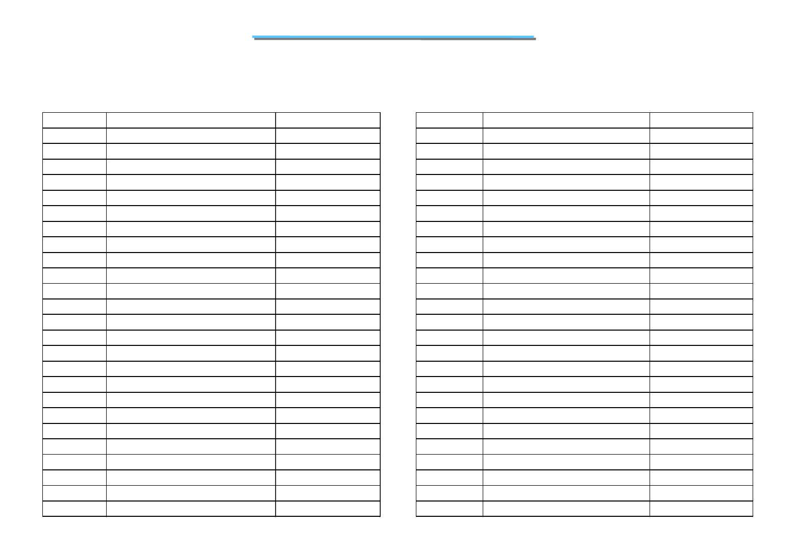
187
8170 N/B MAINTENANCE
9. Spare Parts List -- All (8)
Part Number Description Location(s)
345669900004 RUBBER;LCD,DOWN,7170
345671200001 RUBBER;LCD,UP,8170
565167120001 S/W;CD ROM,SYSTEM,8170
565180626001 S/W;CD*1,DVD,WIN-DVD,INTERVIDEO
340671200013 SCREW ASSY;CPU,8170
340671200014 SCREW ASSY;IC,82845,8170
371102011502 SCREW;M2L15,FLT(+),NIW/NLK
323760000002 SDRAM MODULE;256M,8M*16,PC133,SP
340671200005 SHIELDING ASSY;TOP,8170
561860000022 SINGLE PAGE;GN,NOTE FOR BATTERY&
370102610302 SPC-SCREW;M2.6L3,NIB,K-HD,NYLOK
370102610405 SPC-SCREW;M2.6L4,NIW,K-HD,t=0.8,
370102610405 SPC-SCREW;M2.6L4,NIW,K-HD,t=0.8,
370102630601 SPC-SCREW;M2.6L6,HDt0.5,NIWNLK
370102610805 SPC-SCREW;M2.6L8,K-HD,NIW/NLK
370102010205 SPC-SCREW;M2L2(t0.3),N/W/WLK
370102010256 SPC-SCREW;M2L2.5,K-HD(t0.5) NLK,
370102010256 SPC-SCREW;M2L2.5,K-HD(t0.5) NLK,
370102010309 SPC-SCREW;M2L3.0,NIW/NLK,HD07
370102010407 SPC-SCREW;M2L4,K-HD,NIB/NLK
370102010405 SPC-SCREW;M2L4,NIW,K-HD(+),NYLOK
370102010405 SPC-SCREW;M2L4,NIW,K-HD(+),NYLOK
370102010608 SPC-SCREW;M2L6,KD,HDψ 3 ,NIB/NL
370102010606 SPC-SCREW;M2L6,K-HD(t0.2),NIB/NL
370102010605 SPC-SCREW;M2L6,NIW,HDT=0.4,779
Part Number Description Location(s)
370103010405 SPC-SCREW;M3L4,NIW,K-HD,T0.3
370103010604 SPC-SCREW;M3L6,NIB,K-HD,t0.8,NYL
340671200012 SPEAKER ASSY;R,8170
340671200019 SPERKER ASSY;L,8170
377244010002 STANDOFF;#4-40DP3.5H5L5.5,NIW
341668300008 STANDOFF;MDC MODEM,NLK,HOPE
297040105012 SW;PUSH BUTTOM,4P,SP,12V/50MA,H2 SW1,SW2,SW3,SW4,SW5,SW
6
297040105010 SW;PUSH BUTTOM,5P,SPST,12V/50MA, SW1,SW2,SW3,SW4
297030105003 SW;TOGGLE,SPST,5V/1mA,MPU-101-80 SW6
346671200002 THERMAL PAD;HEATSINK,CPU,8170
310111103012 THERMISTOR;10K,1%,RA,0603,1P R4
340669900002 TILT UNIT;L,7170
340669900001 TILT UNIT;R,7170
442164900010 TOUCH PAD MODULE;TM41PD-350
288227002001 TRANS;2N7002LT1,N-CHANNEL FET PQ500,PQ501,PQ506,PQ507
288227002001 TRANS;2N7002LT1,N-CHANNEL FET PQ1,PQ3
288203400001 TRANS;AO3400,N-MOSFET,SOT-23 Q13,Q503
288203401001 TRANS;AO3401,P-MOSFET,SOT-23 PQ1,PQ512,Q1,Q509
288204400001 TRANS;AO4400,N-MOSFET,SO-8 PU13,Q500,U505
288204400001 TRANS;AO4400,N-MOSFET,SO-8 PU501,PU504
288200144002 TRANS;DTA144WK,PNP,SMT Q514
288200144003 TRANS;DTC144TKA,N-MOSFET,SOT-23 PQ511,Q10,Q15,Q2,Q506,Q
5
288200144001 TRANS;DTC144WK,NPN,SOT-23,SMT PQ2,PQ509,Q12,Q14,Q3,Q4,
288200302001 TRANS;FDV302P,P-CHANNEL,SOT23 Q7
288203906018 TRANS;MMBT3906L,PNP,Tr35NS,TO236 PQ505
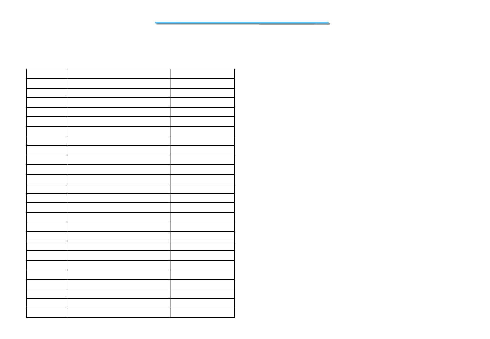
188
8170 N/B MAINTENANCE
9. Spare Parts List -- All (9)
Part Number Description Location(s)
288202303001 TRANS;SI2303DS,P-MOSFET,SOT-23 PQ2
288104362001 TRANS;SI4362DY,N-HOSFET,S08 PU1,PU2,PU501,PU502,PU5
288204800001 TRANS;SI4800DY,N-MOS,.0185OHM,SO PU5
288204800001 TRANS;SI4800DY,N-MOS,.0185OHM,SO PU503,PU506
288204832001 TRANS;SI4832DY,N-MOSFET,.028OHM, PU6
288204832001 TRANS;SI4832DY,N-MOSFET,.028OHM, PU502,PU505
288204835001 TRANS;SI4835DY,PMOS,6A/30V,.035, PU10,PU11,PU512,PU9
288204835001 TRANS;SI4835DY,PMOS,6A/30V,.035, PQ502,PQ503
288204892001 TRANS;SI4892DY,N-MOSFET,SO8 PU500,PU503,PU506,PU507
273001050065 TRANSFORMER;10/100 BASE,LF-H72P, U2
373101710301 T-SCREW;I,M1.7,L3,K-HD,D3.0,NIB
373002010002 T-SCREW;S.M2 L4, PAN(+),NIW
373002010003 T-SCREW;S.M2 L5, PAN(+),NIW
270140000003 VARISTOR;280V,5.6X3.8MM,TVB280-0 S500
271911103906 VR;10K,20%,0.05W,RN101GAC10KPGJ- VR1
421671200004 WIRE ASSY;HANNSTAR,14.1",SXGA,LC
421671200007 WIRE ASSY;INVERTER,8170
421671200008 WIRE ASSY;MDC,8170
421669900007 WIRE ASSY;TOUCHPAD,7170
274011431408 XTAL;14.318M,50PPM,32PF,7*5,4P,S X502
274011600408 XTAL;16MHZ,16PF,50PPM,8*4.5,2P X503
274012457406 XTAL;24.576MHZ,16PF,50PPM,8*4.5, X1,X2
274012500401 XTAL;25MHZ,30PPM,18PF,4P,SMT X501
274012700401 XTAL;27MHZ,20PPM,16PF,7*5,4P,SMT X500
274013276114 XTAL;32.768KHZ,10PPM,12.5PF X3
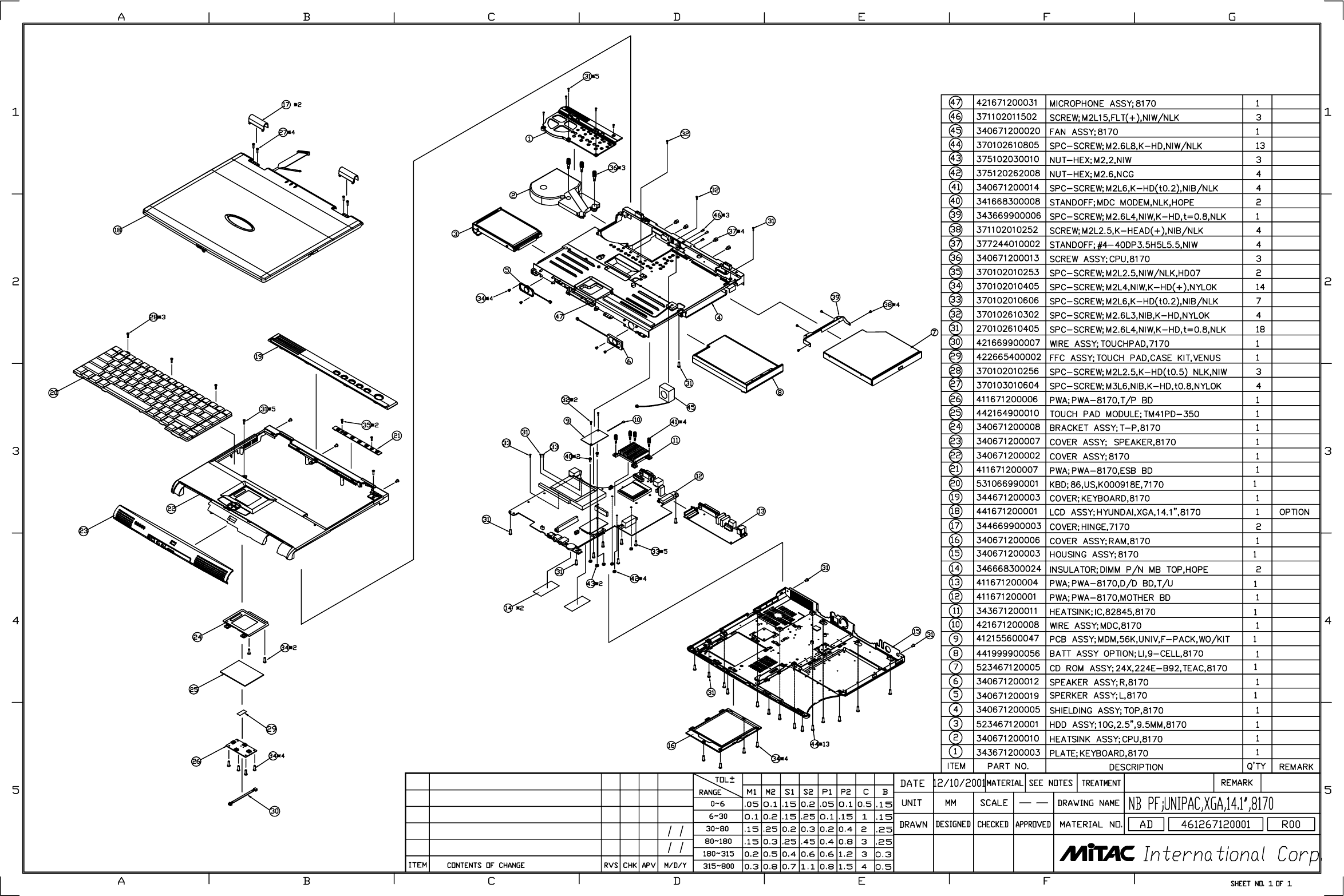
A
A
B
B
2 2
1 1
Contexts
Title
Page
P4-CPU (1/2)
P4-CPU (2/2)
BROOKDALE-MCH845(1/2)
VGA-M6(1/2)
SO-DIMM Memory X 2
PCMCIA/1394 Controller(PCI4410) & Socket
Micro Controller(H8)
Audio Codec & Amplifier
Clock Generator,Screw holes
HDD, CDROM Connector & PULL-UP RESISTER
TOUCH PAD,BIOS,SUPER-IO
2
3
4
5
6
7
8
9
10
11
12
Cover Sheet
System Block Diagram
1
13
Battery Connector &3V,5V-RESUME POWER
14
15
16
History of Schematics
Revision 0A (EVT)
DRAW DESIGN CHECK ISSUED
MODEL : 8170 Revision 02
17
Power Block Diagram
LCD & CRT Interface
VGA-M6(2/2)
19
20
21
LANPHY,MDC
18
CPU Vcore,1.8V,1.5V
22
INTD USB1/LAN
-REQ0/-GNT0
CHIP
LAN
AD11
AD18
INTC
IDSEL
AD19
REQ/GNT
CHIP
-REQ1/-GNT1
INTA
CHIP
INTH
-REQ2/-GNT2AD18
NU
PCIINT
PCMCIA
PCMCIA
LAN
X
X
X
LOW
STR
LOW
-SUSC HIGH
X+5V
+12V O
O
+5V
+12V
+5VA
X
+12V
+1.8V
X+3V
+3.3V
STATE STD
O
O
O
X
O
X
VDDR_MEM2.5
CPU_CORE
+3VS
LOW
OADP
+5VS
X
HIGH
+1.8V
X
X
X
O
+5V
VOTAGE
O
HIGH
MEC-OFF
O
LOW
O
O+3.3V
O
0
LOW
-SUSB
O
+3V_ICH
RTC_VCC
O
X
O
-
OO
+12VS
BATTERY
O
O
X
X
FULL ON
X
XX
SIGNAL
POWER STATES
X
O
REMARK
O
+1.75V
0
X
+19V
O
-
O
O
O
+12V
+2.5V
IDSEL BUS MASTER
PCIINT
PCMCIA/ATI VGA
BROOKDALE-MCH845(2/2)
ICH2
DC-DC CONNECTOR,CHARGER
-REQ3/-GNT3
NU-REQ4/-GNT4
PCMCIA/1394
+1.8V_ICH
+1.8VS
USB2
OX X X
OO
+3.3V
+3.3V
O
+5V
1
2
3
4
5
6
7
8
COMP
GND
GND
IN-2
GND
SOLDER
POWER
IN-1
Revision 0B (DVT)
X
XX
X
X
1.ADD 1UF FOR ADM1021A Temperature Monitor.
2.DEL EMAIL BTN SW5 AND D16 LED INCICATOR.
3.+1.8VA CHANGE (+1.8V_ICH) FOR ICH2.
4.+3VA CHANGE (+3V_ICH) FOR ICH2.
5.-PCIRST CONTROL HDD & CD_ROM RESET,CHANGE VON GPIO PIN EACH RESET FOR S3 WEAKUP.
6.ADD TWO 10K PULL_UP RESISTOR FOR H8 THERMAL SENSE ,TWO FAN FREEBACK SCHEMATIC.
7.ADD U515 & CHANGE J5 FOR 8170 QK/B AND 8175 LED/B COMMON.
8.ADD -LID PIN ON J6 FOR 8175 COVER SWITCH.
9.MODIFY TOUCH_PAD +5VS CHANGE +5VS.
10.MODIFY LANPHY +3VS CHANGE +3V.
11.MODIFY ICH2 +5VA CHANGE +5V.
12.MODIFY RTC CIRCUITRY +3VA CHANGE +5VA VON 330K & 1M DIVIDER.
Revision 01 (PVT)
2.ADD C717 &C718 (4.7U) for boot time "popo"tone.
3.ADD R162 modify 2M BIOS pull +5VS.
4.Change SDRAM Q8 for IO_DATA ram module.
5.ADD 1U CAP for inverter RED too light.
6.IEEE1394 modify 1394_GND of digital GND for ESD issue.
7.MDC modify to digital GND.
1.ADD DIODE FOR S.B +5VS DRAIN.
8.Modify FAN feedback +5V change +5VS and FAN control pin modify +5VS change +5V.
9.Second fan modify connect Vertical to Horizontally.
1.CHANGE CAP 0.068U OF 0603 TO 0805.
2.LAN OF MA8(PIN61) PULL HI +3V.
3.R163,R164,R696,R697,L535 CHANGE OF DFS FOR COST DOWN.
4.AMP(MUTE IN) ADD PULL HI +5VS.
5.LCD CONNECT PROVISION 5P CAP.
02
Cover Sheet
122Friday, December 28, 2001
C411671200001
Title
Size Document
Number
Rev
Date: Sheet of
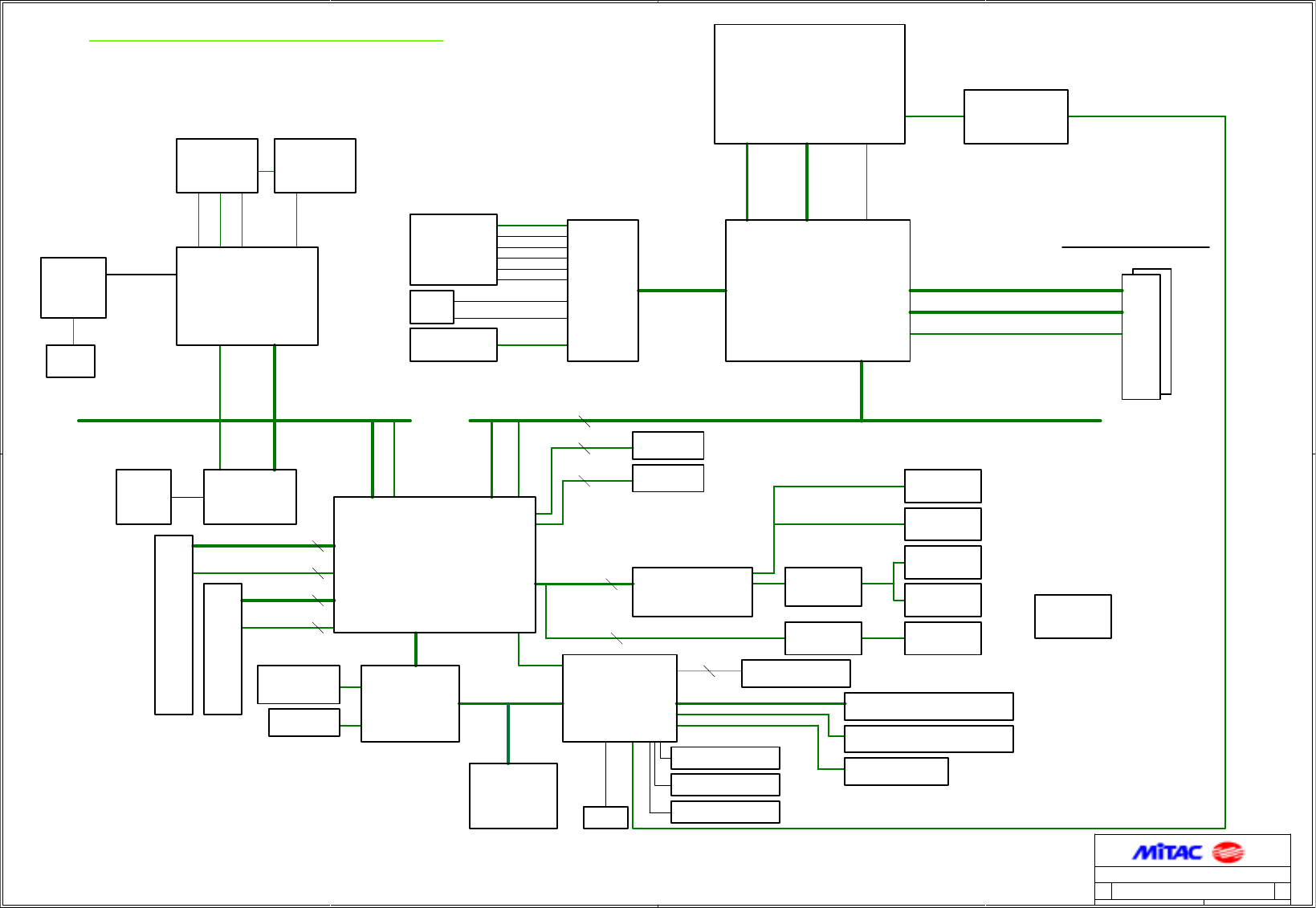
A
A
B
B
2 2
1 1
Brookdale
MCH
BGA 593
SO-DIMM
MD[0..63]
MA[0..14]
DRAM Control
TPS2211
SSOP 16
AD[0..31]
PCMCIA/1394 LINK
PCI 4410
CONTROLLER
Control
uBGA 209
PCI BUS
Micro-FCPGA 478 pin
CRT
HSYNC
G
R
VSYNC
B
DDC
8170 System Block Diagram
ICH2
SD[0..15]
Primary EIDE
(HDD)
USB1
Control
BGA 421
Control
USB0
Secondary EIDE
(CDROM/DVD)
PD[0..15]
Audio Codec
AC Link
Amplifier
H8-3437
External Keyboard
Internal Keyboard
Touch PAD
JACK
M.D.C. JACK
Power Button
FAN1 For CPU
144 Pin SO-DIMM Socket*2
-HD[0..63]
-HA3..31]
Control
Pentium 4
A[0..25]
D[0..15]
IC CARD
Socket
Control
16MHz
ADM 1021
PQFP 100
Realtek ALC201
PQFP 48
TPA 0202
C.P.U.
Keyboard Controller
Power Switch
Thermal Recorder
SPDIF
RJ-11
Internal
Speaker
Internal
Microphone
External
Microphone
Control
AD[0..31]
Control
RJ45
1394
PHY
TSB41AB1
TI PQFP64
(30 pin) ICS950805
Clock
Generator
TQFP 100PIN
NS87393
14.1"/15.1"
TFT LCD
LVDS DATA
Y
C
S
Vedio
Willamette/Northwood
AGP BUS 4X
ATI
M6
VGA
BGA 484
RTL8139CL
LQFP 128
Control
AD[0..31]
Controller 0
Controller 1
FAN2 For D/D
Super I/O
Intel 82801BA
LPC
ISA BUS
Flash ROM
512KB
PLCC 32
PRINTER
PORT
HP-3600
IR Module
3
3
5
5
16
16
MINI
1394
HUB[0..11]
HUB LINK
Control
13
1
Cover Switch
02
System Block Diagram
222Friday, December 28, 2001
411671200001
Title
Size Document
Number
Rev
Date: Sheet of
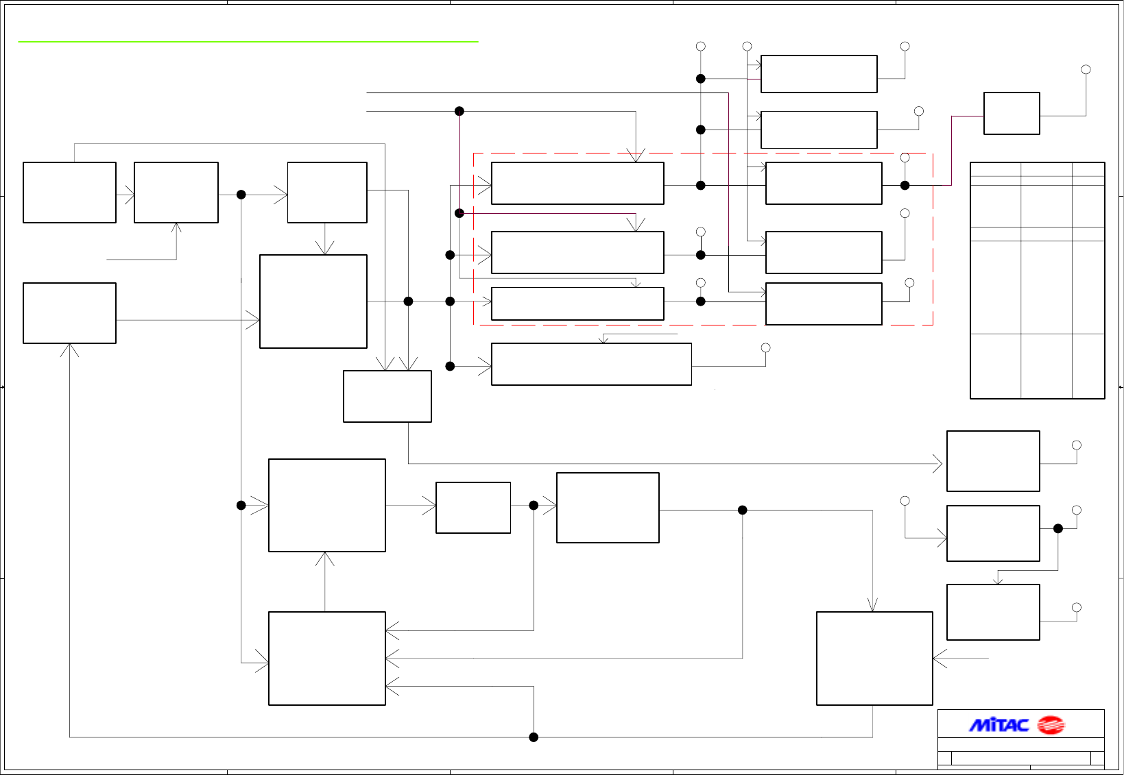
5
5
4
4
3
3
2
2
1
1
D D
C C
B B
A A
POWER DIAGRAM OF THE 8170
ADAPTOR Protecter
Diode
P Channel
MOSFET
SI4835DY
Battery
Pack Discharge
+5VA
+12V
D/VMAIN
5V DC to DC Convertor
+3V
Vcc Core DC to DC Convertor
LTC1709-9
CPU_CORE
3.3V DC to DC Convertor
+5V
DC/DC BOARD
PWR_ON
Shut Down
High
Low
Side
CC
1.8VS
Rsense
Charge
Regulator
LP2951
CV
CC
PWM
Charge IC
MAX1772
Self
Dischange
learning
Diode
Always
Charge
CHARGE
SWITCH
SI4925DY
Choke +3V_ICH
Regulator
TC55RP3302
EMB
MOSFET
Shut Down
+3VS
Shut Down
MOSFET
+5VS
SUSB#
MOSFET
Shut Down
+12VS
CPU_CORE_EN
+1.8V_ICH
MUST BE MEET ICH2
POWER ON SEQUENCE
MUST BE MEET ICH2
POWER ON SEQUENCE
CPU_CORE CPU(FOR 1.7G) 49.3A
+3V MCH
SODIMM
M6
ICH2
RTL8139CL
2A
?
330mA
410mA
330mA
+1.5VS MCH
ATI_M6 20mA
?
VDDR_MEM2.5 ATI_M6
+1.8V *ATI_M6
+1.8VS MCH
470mA
1200mA
350mA
350mA
+1.8VA ICH2 5mA
ATI_M6
1200mA
ICH2
280mA
+3VA
IDE
+5VS
15mA
CD-ROM
20mAM6
+5V
CLOCK
900mA
+3VS
+5VA
ICH2
IEEE1394
PCI4410 79mA
69mA
SIO
*MCH
ICH2 410mA
50mA
?
LCD 800mA
* OPTION(NO LINK)
ALC200 40mA
1500mA
?
H8 40mA
USBX2 1000mA
AUDIO AMP 1000mA
MODEM
PCMCIA CARD
PCMCIA CARD 500mA
500mA
VDDR_MEM2.5
(FOR VGA)
+1.5VS
Regulator
AME8801
MOSFET
Shut Down
+12VS
Shut Down
12V DC to DC Convertor
Shut Down
MOSFET
Shut Down
+5V
411671200001 02
Power Block Diagram
322Friday, December 28, 2001
Title
Size Document
Number
Rev
Date: Sheet of
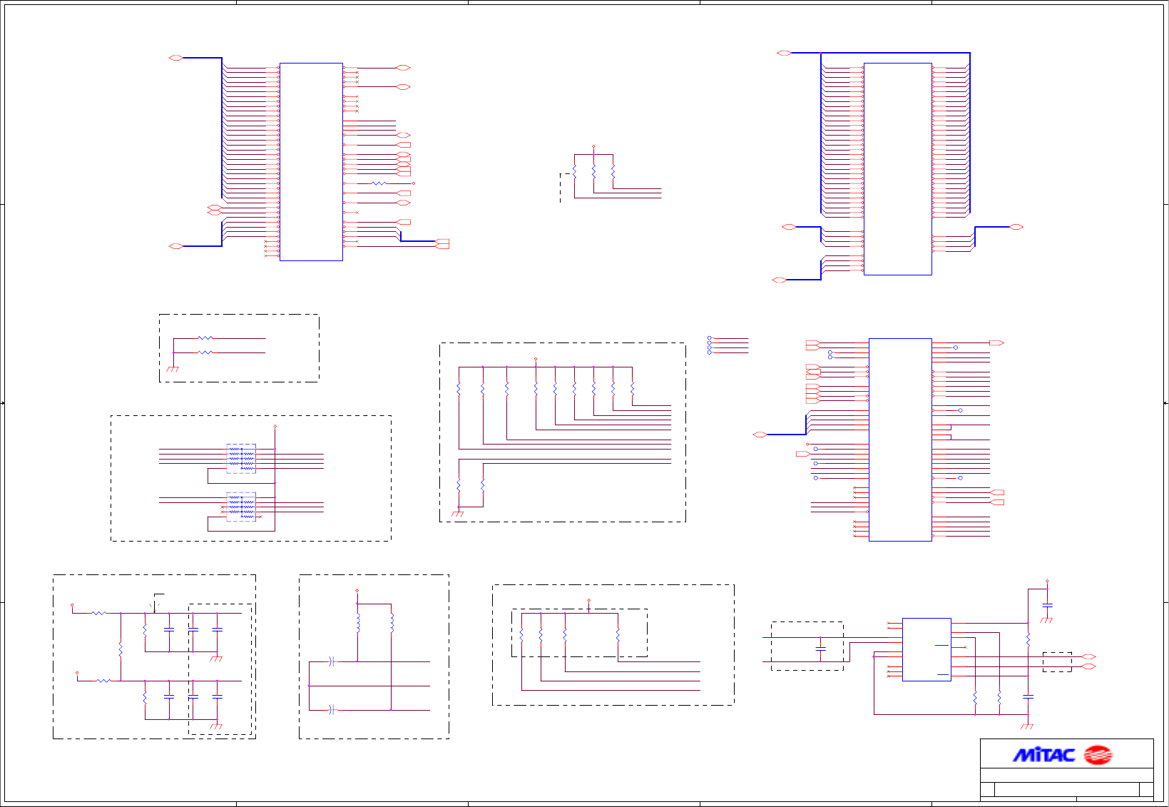
5
5
4
4
3
3
2
2
1
1
D D
C C
B B
A A
PLL SUPPLY FILTER
GTL Reference CKT
One 220PF for each GTL REF Pin
PLACE THESE INSIDE SOCKET CAVITY
PRECISION FSB COMPENSATION RESISTORS
REQUEST NEW PART NUMBER FOR 51.1 Ohm, 1%
PLACE CLOSE TO CPU SOCKET
PLACE AT CPU END
CPU SIGNAL TERMINATION
4" MAX.
Close to CPU socket
PLACE AT CPU END
THERMAL RECORDER
W/S=12/12 mils
(
!"#$##
as short as
possible
Layout Note:
W=12mil
DESIGN GUIDE PAGE 236
DESCRIPTION(NO extra pull-up
resistors required)
411671200001 02
P4-CPU(1/2)
Custom
422Friday, December 28, 2001
Title
Size Document
Number
Rev
Date: Sheet of
-HA3
-HA4
-HA5
-HA6
-HA7
-HA8
-HA9
-HA10
-HA11
-HA12
-HA13
-HA14
-HA18
-HA17
-HA16
-HA15
-HA19
-HA20
-HA21
-HA22
-HA26
-HA25
-HA24
-HA23
-HA31
-HA27
-HA30
-HA28
-H_REQ4
-H_ADSTB0
-H_ADSTB1
-HA29
-HA[3..31]
-H_REQ3
-H_REQ2
-H_REQ1
-H_REQ0
-H_ADS
-H_BNR
TESTHI8
TESTHI9
TESTHI10
-H_BR0
-H_BPRI
-H_DBSY
-H_DEFER
-H_DRDY
-H_HIT
-H_HITM
-H_INIT
-H_LOCK
-H_RS2
-CPURST
-H_RS1
-H_RS0
-H_TRDY
-HD31
-HD30
-HD29
-HD28
-HD27
-HD26
-HD24
-HD25
-HD23
-HD22
-HD20
-HD21
-HD19
-HD17
-HD16
-HD18
-HD15
-HD14
-HD12
-HD13
-HD11
-HD9
-HD8
-HD10
-HD5
-HD4
-HD0
-HD1
-HD7
-HD3
-HD6
-HD2
-HD32
-HD33
-HD34
-HD35
-HD36
-HD37
-HD39
-HD38
-HD40
-HD41
-HD43
-HD42
-HD44
-HD47
-HD45
-HD46
-HD48
-HD49
-HD51
-HD50
-HD52
-HD55
-HD53
-HD54
-HD60
-HD58
-HD63
-HD57
-HD56
-HD62
-HD61
-HD59
-H_REQ[0..4] -H_RS[0..2]
-DBI0
-DBI1
-DBI2
-DBI3
-DSTBN0
-DSTBN1
-DSTBN2
-DSTBN3
-DSTBP0
-DSTBP1
-DSTBP2
-DSTBP3
-DBI[0..3]
-DSTBN[0..3]
-DSTBP[0..3]
H_COMP0
H_COMP1
-H_INIT
-HD[0..63]
ITP_TMS
-ITP_RESET
H_PWRGD
-H_BR0
-CPURST
TESTHI11 TESTHI8TESTHI12
-H_BMP2
-H_BMP1
-H_BMP0
ITP_TDO
ITP_TDI
TESTHI9
TESTHI10
TESTHI5
TESTHI4
TESTHI7
TESTHI6
TESTHI0
TESTHI2
TESTHI1
TESTHI3
-THRMTRIP
-H_BMP5
PLL_VSSA
CPU_THERMDA
ITP_TCK
-H_PROCHOT
-H_IGNNE
H_COMP1
H_COMP0
-SLP
PVID4
ITP_TCK
HCLK_CPU
-H_SMI
-H_BMP4
-H_BMP0
TESTHI3
CPU_THERMDC
TESTHI1
H_NMI
-H_STPCLK
PVID1
PLL_VCCA
-H_BMP5
TESTHI4
ITP_TDO
PLL_VSSA
-H_BMP1
TESTHI5
-H_A20M
PVID3
PLL_VCCA
H_GTLREF2_3
H_INTR -H_BMP2
TESTHI0
TESTHI2
ITP_TDI
CPU_THERMDA
-H_BMP4
ITP_TMS
PVID0
CPU_THERMDC
-H_PROCHOT
TESTHI12
TESTHI7
-ITP_RESET
-HCLK_CPU
H_GTLREF2_3
-H_FERR
-H_BMP3
-THRMTRIP
CPU_GTLREF
-H_BMP3
PVID[0..4]
TESTHI6
H_PWRGD
PVID2
CPU_GTLREF
-H_FERR
VCCIO_PLL
H_BSEL0
TESTHI11
VCCIO_PLL
-H_A20M
-H_IGNNE
H_INTR
H_NMI
CPU_CORE
CPU_CORE
CPU_CORE
CPU_CORE
+5VS
CPU_CORE
CPU_CORE
CPU_CORE
CPU_CORE
CPU_CORE
R7
51.1 0603
1%
1 2
C545
1U
0805
5%
12
R515
51
0603
12
C547
220P
0603
5%
12
R525
100
0603
1%
12
TP8 1
TP1 1
R3
62
0603
12
R2
62
0603
12
R514
75
0603
12
R507
51.1 0603
1%
1 2
R509
300/NA
0603
1%
12
TP5
1
C536
0.1U
50V
0603
12
C524
220P
0603
5%
12
R517
62
0603
1%
12
R5
301
0603
12
R521
39
0603
12
C523
220P
0603
5%
12
TP2
1
C522
1U
0805
5%
12
R508
51
0603
12
R510
51
0603
12
R523
0_DFS
0603
12
R524
0_DFS
0603
12
C531
2200P
0603
12
TP547 1
TP42 1
TP41 1
TP40 1
U502
ADM1021 QSOP16B
1
3
4
5
6
7
8
9
10
11
12
13
14
15
16 2
TEST
D+
D-
NC1
ADD1
GND1
GND2
NC2
ADD0
ALERT
SDATA
NC3
SCLK
STBY
TEST1 VDD
R506 62 06031%
1 2
L3
4.7UH
2012
12
L2
4.7UH
2012
12
C715
1U
0603
12
R526
10K
0603
12
+
C30
33U16V
7343
20% 12
+
C31
33U16V
7343
20% 12
R513
51
0603
12
TP4 1
TP3 1
TP6 1
R512
51
0603
12
R6
51
0603
12
TP7
1
R516
51
0603
12
U1A
WMT478/NWD_14
G1
AC1
V5
AA3
G2
L25
K26
K25
J26
U6
W4
Y3
H6
D2
H5
E2
H2
F3
E3
AC3
W5
G4
V6
AB25
F4
G5
F1
AB2
J6
N5
N4
N2
M1
N1
M4
M3
L2
M6
L3
K1
L6
K4
K2
L5
H3
J3
J4
K5
J1
AB1
Y1
W2
V3
U4
T5
W1
R6
V2
T4
U3
P6
U1
T2
R3
P4
P3
R2
T1
R5
ADS#
AP#0
AP#1
BINIT#
BNR#
DP#3
DP#2
DP#1
DP#0
TESTHI8
TESTHI9
TESTHI10
BR#0
BPRI#
DBSY#
DEFER#
DRDY#
HIT#
HITM#
IERR#
INIT#
LOCK#
MCERR#
RESET#
RS#2
RS#1
RS#0
RSP#
TRDY#
A#16
A#15
A#14
A#13
A#12
A#11
A#10
A#9
A#8
A#7
A#6
A#5
A#4
A#3
ADSTB#0
REQ#4
REQ#3
REQ#2
REQ#1
REQ#0
A#35
A#34
A#33
A#32
A#31
A#30
A#29
A#28
A#27
A#26
A#25
A#24
A#23
A#22
A#21
A#20
A#19
A#18
A#17
ADSTB#1
R522
680
0603
12
R518
0/NA
0603
1 2
R520
49.9 0603
1%
1 2
RP505
1K*8 1206
1
2
3
4
5 6
7
8
9
10
R519
51
0603
12
RP2
1K*8 1206
1
2
3
4
5 6
7
8
9
10
R502
27
0603
12
R503
150
0603
12
R527
49.9 0603
1%
1 2
U1C
WMT478/NWD_14
AD6
AD5
A6
L24
P1
AB4
AA5
Y6
AC4
AB5
AC6
AD24
AE25
AD25
AA6
F6
AA21
F20
AC23
AC24
AC20
AC21
AB22
AA20
AA2
AB23
C3
AB26
D4
C1
D5
F7
E6
AF22
AF23
AC26
AD26
C6
B6
B2
D1
E5
B5
Y4
AE1
AE2
AE3
AE4
AE5
AF2
AF4
AD20
A5
AE23
AD22
A4
AE21
A22
A7
B3
C4
A2
AD3
AF25
AD2
AF24
AF3
AF26
BSEL0
BSEL1
TESTHI11
COMP0
COMP1
BPM#5
BPM#4
BPM#3
BPM#2
BPM#1
BPM#0
TESTHI0
DBR#
TESTHI12
GTLREF3
GTLREF2
GTLREF1
GTLREF0
TESTHI5
TESTHI4
TESTHI3
TESTHI2
TESTHI7
TESTHI6
TESTHI1
PWRGOOD
PROCHOT#
SLP#
TCK
TDI
TDO
TMS
TRST#
BCLK0
BCLK1
ITP_CLK0
ITP_CLK1
A20M#
FERR#
IGNNE#
LINT0
LINT1
SMI#
STPCLK#
VID4
VID3
VID2
VID1
VID0
VCC
VCCVID
VCCA
VCCSENSE
VCCIOPLL
VSSA
VSSSENSE
RSVD
RSVD
RSVD
THRMDA
THRMDC
THRMTRIP#
RSVD
RSVD
RSVD
RSVD
RSVD
SKTOCC#
R511
100
0603
1%
12
U1B
WMT478/NWD_14
M23
N22
P21
M24
N23
M26
N26
N25
R21
P24
R25
R24
T26
T25
T22
T23
P26
R22
P23
U26
U24
U23
V25
U21
V22
V24
W26
Y26
W25
Y23
Y24
Y21
AA25
AA22
AA24
V21
W22
W23
B21
B22
A23
A25
C21
D22
B24
C23
C24
B25
G22
H21
C26
D23
J21
D25
E21
E22
F21
H22
E24
G23
F23
F24
E25
F26
D26
L21
G26
H24
M21
L22
J24
K23
H25
G25
K22
J23
D#32
D#33
D#34
D#35
D#36
D#37
D#38
D#39
D#40
D#41
D#42
D#43
D#44
D#45
D#46
D#47
DBI#2
DSTBN#2
DSTBP#2
D#48
D#49
D#50
D#51
D#52
D#53
D#54
D#55
D#56
D#57
D#58
D#59
D#60
D#61
D#62
D#63
DBI#3
DSTBN#3
DSTBP#3
D#0
D#1
D#2
D#3
D#4
D#5
D#6
D#7
D#8
D#9
D#10
D#11
D#12
D#13
D#14
D#15
DBI#0
DSTBN#0
DSTBP#0
D#16
D#17
D#18
D#19
D#20
D#21
D#22
D#23
D#24
D#25
D#26
D#27
D#28
D#29
D#30
D#31
DBI#1
DSTBN#1
DSTBP#1
C546
220P
0603
5%
12
-HA[3..31](6) -HD[0..63](6)
-H_REQ[0..4](6)
-H_ADSTB0(6) -H_ADSTB1(6)
-H_ADS (6)
-H_BNR (6)
-H_BPRI (6)
-H_BR0 (6)
-H_DBSY (6)
-H_DRDY (6)
-H_LOCK (6)
-H_TRDY (6)
-CPURST (6)
-H_INIT (13)
-H_HIT (6)
-H_HITM (6)
-H_RS[0..2] (6)
-DBI[0..3](6)
-DSTBN[0..3](6)
-DSTBP[0..3] (6)
-H_DEFER (6)
H8_THRM_DATA (19)
H8_THRM_CLK (19)
-H_STPCLK(13) -H_SMI(13)
H_NMI(13)
HCLK_CPU(8)
H_PWRGD (13)
PVID[0..4](21)
H_INTR(13)
VCCPVID(5)
-H_IGNNE(13)
-H_A20M(13)
-SLP (13)
H_BSEL0 (8)
-H_FERR(13)
-HCLK_CPU(8)
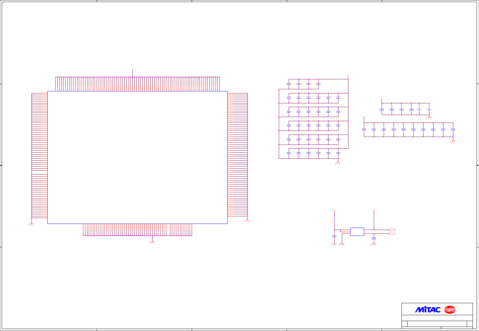
5
5
4
4
3
3
2
2
1
1
D D
C C
B B
A A
411671200001 02
P4-CPU(2/2)
Custom
522Friday, December 28, 2001
Title
Size Document
Number
Rev
Date: Sheet of
VCCPVID
CPU_CORE_EN
CPU_CORE
CPU_CORE
+5VS +5VS
CPU_CORE
CPU_CORE
+
C28
150U
10V
7343
12
+
C12
150U
10V
7343
12
R505
10K
0603
12
C548
0.1U
50V
0603
12
C533
0.1U
50V
0603
12
C549
0.1U
50V
0603
12
C532
0.1U
50V
0603
12
C539
0.1U
50V
0603
12
C540
0.1U
50V
0603
12
C22
0.1U
50V
0603
12
C538
0.1U
50V
0603
12
C544
0.1U
50V
0603
12
C534
0.1U
50V
0603
12
C516
1U
0603
12
C15
10U
10V
1206
12
C541
10U
10V
1206
12
C20
10U
10V
1206
12
C25
10U
10V
1206
12
C528
10U
10V
1206
12
C542
10U
10V
1206
12
C514
22U
10V
1210
12
C10
10U
10V
1206
12
C8
22U
10V
1210
12
C518
10U
10V
1206
12
C29
10U
10V
1206
12
C513
10U
10V
1206
12
C17
10U
10V
1206
12
U1D
WMT478/NWD_14
AE7
AE24
AE22
AE19
AD14
AD12
AD10
AD8
AD4
AD1
AD23
AD21
AE17
AE15
AE13
AE11
AE9
AE26
AB20
AC17
AC15
AC13
AC11
AC9
AC7
AC5
AC2
AC25
AC22
AC19
AD18
AD16
AA4
AA1
AA23
AA19
AB18
AB16
AB14
AB12
N6
N3
N24
N21
P5
P2
P25
P22
R26
R4
R1
R23
T6
T3
T24
T21
U5
U2
U25
U22
V26
G21
H26
H4
H1
H23
J5
J2
J25
J22
K6
K3
K24
K21
L26
L4
L1
L23
M5
M2 AB10
AB8
AB6
AB3
AB24
AB21
V4
V1
V23
W6
W3
W24
W21
Y5
Y2
Y25
Y22
AA17
AA15
AA11
M25
M22
E11
E9
E26
E7
E4
E1
E23
E19
F18
F16
F14
F12
F10
F8
F5
F2
F25
F22 AA9
AA26
AA7
G6
G3
G24
C5
C2
C25
C22
C19
D18
D16
D14
D12
D10
D8
D6
D3
D24
D21
D20
E17
E15
E13
A3
A24
A21
A19
B18
B16
B12
B10
B26
B8
B4
B23
B20
C17
C15
C13
C11
C9
C7
AF18
AF16
AF14
AF12
AF10
AF8
AF6
AF1
AF20
A17
A15
A13
A11
A9
A26
AD11
AD9
AD7
AE18
AE16
AE14
AE12
AE10
AE8
AE6
AE20
AB15
AB13
AB11
AB9
AB7
AB19
AC18
AC16
AC14
AC12
AC10
AC8
AD17
AD15
AD13
E14
E12
E10
E8
E20
F17
F15
F13
F11
F9
F19
AA18
AA16
AA14
AA12
AA10
AA8
AB17
B13
B11
B9
B7
B19
C18
C16
C14
C12
C10
C8
C20
D17
D15
D13
D11
D9
D7
D19
E18
E16
AF17
AF15
AF13
AF11
AF9
AF7
AF5
AF21
AF19
A18
A16
A14
A12
A10
B17
B15
A20
A8
AD19
AA13
B14
VSS
VSS
VSS
VSS
VSS
VSS
VSS
VSS
VSS
VSS
VSS
VSS
VSS
VSS
VSS
VSS
VSS
VSS
VSS
VSS
VSS
VSS
VSS
VSS
VSS
VSS
VSS
VSS
VSS
VSS
VSS
VSS
VSS
VSS
VSS
VSS
VSS
VSS
VSS
VSS
VSS
VSS
VSS
VSS
VSS
VSS
VSS
VSS
VSS
VSS
VSS
VSS
VSS
VSS
VSS
VSS
VSS
VSS
VSS
VSS
VSS
VSS
VSS
VSS
VSS
VSS
VSS
VSS
VSS
VSS
VSS
VSS
VSS
VSS
VSS
VSS
VSS
VSS
VSS
VSS VSS
VSS
VSS
VSS
VSS
VSS
VSS
VSS
VSS
VSS
VSS
VSS
VSS
VSS
VSS
VSS
VSS
VSS
VSS
VSS
VSS
VSS
VSS
VSS
VSS
VSS
VSS
VSS
VSS
VSS
VSS
VSS
VSS
VSS
VSS
VSS
VSS
VSS
VSS
VSS VSS
VSS
VSS
VSS
VSS
VSS
VSS
VSS
VSS
VSS
VSS
VSS
VSS
VSS
VSS
VSS
VSS
VSS
VSS
VSS
VSS
VSS
VSS
VSS
VSS
VSS
VSS
VSS
VSS
VSS
VSS
VSS
VSS
VSS
VSS
VSS
VSS
VSS
VSS
VSS
VSS
VSS
VSS
VSS
VSS
VSS
VSS
VSS
VSS
VSS
VSS
VSS
VSS
VSS
VSS
VSS
VSS
VSS
VSS
VCC
VCC
VCC
VCC
VCC
VCC
VCC
VCC
VCC
VCC
VCC
VCC
VCC
VCC
VCC
VCC
VCC
VCC
VCC
VCC
VCC
VCC
VCC
VCC
VCC
VCC
VCC
VCC
VCC
VCC
VCC
VCC
VCC
VCC
VCC
VCC
VCC
VCC
VCC
VCC
VCC
VCC
VCC
VCC
VCC
VCC
VCC
VCC
VCC
VCC
VCC
VCC
VCC
VCC
VCC
VCC
VCC
VCC
VCC
VCC
VCC
VCC
VCC
VCC
VCC
VCC
VCC
VCC
VCC
VCC
VCC
VCC
VCC
VCC
VCC
VCC
VCC
VCC
VCC
VCC
VCC
VCC
VCC
VCC
VSS
VSS
C19
10U
10V
1206
12
C23
10U
10V
1206
12
C551
10U
10V
1206
12
C14
10U
10V
1206
12
C27
10U
10V
1206
12
R504
10
0603
12
C537
10U
10V
1206
12
C16
22U
10V
1210
12
C552
22U
10V
1210
12
C11
10U
10V
1206
12
C521
10U
10V
1206
12
C515
0.1U
16V
0603
10%
12
U501
MIC5248
SOT25
1
2
34
5
IN
GND
EN PG
OUT
C18
10U
10V
1206
12
C26
10U
10V
1206
12
C517
10U
10V
1206
12
C529
10U
10V
1206
12
C525
10U
10V
1206
12
C530
10U
10V
1206
12
C9
10U
10V
1206
12
C550
10U
10V
1206
12
C7
10U
10V
1206
12
C535
10U
10V
1206
12
C543
10U
10V
1206
12
C24
10U
10V
1206
12
C21
10U
10V
1206
12
C13
10U
10V
1206
12
C526
10U
10V
1206
12
VCCPVID (4)
CPU_CORE_EN (21)
5
5
4
4
3
3
2
2
1
1
D D
C C
B B
A A
HXSWING, HYSWING 12 mil trace, 10 mil space
10 mil trace, 7 mil
space, Cap place
near MCH and
between two
resistors.
PLACE AT MCH845 END
411671200001 02
Brookdale-MCH845(1/2)
Custom
622Friday, December 28, 2001
Title
Size Document
Number
Rev
Date: Sheet of
-HA3
-HA4
-HA5
-HA6
-HA7
-HA8
-HA10
-HA9
-HA11
-HA12
-HA14
-HA13
-HA16
-HA15
-HA17
-HA18
-HA19
-HA20
-HA22
-HA21
-HA24
-HA23
-HA25
-HA26
-HA28
-HA27
-HA31
-HA30
-HA29
-HA[3..31]
-HD0
-HD1
-HD2
-HD3
-HD4
-HD5
-HD6
-HD7
-HD8
-HD9
-HD10
-HD11
-HD13
-HD15
-HD12
-HD14
-HD16
-HD17
-HD18
-HD19
-HD21
-HD23
-HD20
-HD22
-HD28
-HD27
-HD31
-HD26
-HD25
-HD30
-HD29
-HD24
-HD32
-HD33
-HD34
-HD35
-HD37
-HD39
-HD36
-HD38
-HD44
-HD43
-HD47
-HD42
-HD41
-HD46
-HD45
-HD40
-HD57
-HD59
-HD56
-HD52
-HD50
-HD55
-HD61
-HD58
-HD60
-HD53
-HD49
-HD63
-HD62
-HD54
-HD48
-HD51
-HD[0..63]
-H_REQ[0..4] -H_REQ0
-H_REQ1
-H_REQ2
-H_REQ3
-H_REQ4
-H_ADSTB0
-H_ADSTB1
-HCLK_MCH
HCLK_MCH
HYSWING
-DSTBP0
-DSTBN0
-DSTBP1
-DBI0
-DBI2
-DSTBP3
-DBI3
-DSTBN3
-DSTBN1
-DBI1
-DSTBN2
-DSTBP2
-DSTBP0
-DSTBN0
-DSTBP1
-DBI0
-DSTBP3
-DBI2
-DBI3
-DSTBN3
-DSTBN1
-DSTBN2
-DSTBP2
-DBI1
-DBI[0..3]
-DSTBN[0..3]
-DSTBP[0..3]
HXRCOMP
HYSWING
-H_ADS
-H_TRDY
-H_DRDY
-H_DEFER
-H_HITM
-H_HIT
-H_BR0
-H_LOCK
-H_BNR
-H_BPRI
-H_RS0
-H_DBSY
-H_RS1
-CPURST
-H_RS2
-H_RS[0..2]
HYRCOMP
CPU_CORE
CPU_CORE
R535
49.9
0603
1%
12
U3D
82845
BGA568_25
W8
W26
Y6
Y22
V8
V6
AC26
AC23
AC21
AC20
AC18
AC4
AC1
AB22
AB19
AB16
AB15
AB14
AB13
AG20
AG18
AG1
AF25
AF21
AF19
AF17
AF15
AF13
AF11
AF9
AF7
AF5
AJ27
AJ17
AJ15
AJ13
AJ11
AJ9
AJ7
AJ5
AJ3
AH23
AH21
AH19
AG22
AD6
AD8
AD10
AD12
AD14
AD16
AD19
AD22
AE1
AE4
AE18
AE20
AE29
P14
P16
W1
W4
AA1
AA4
AA8
AA29
AB6
AB9
AB10
AB12
V22
A15
A11
A7
A3
F24
F20
F16
F12
F8
E29
E26
E4
E1
D21
D17
D13
D9
D5
A27
A23
A19
K27
K7
J29
J26
J22
J6
J4
J1
K5
H21
H19
H17
H15
H13
H11
H9
G26
P8
P6
N29
N22
N17
N15
N13
N8
N4
N1
M23
L26
L24
L22
L8
L6
L4
L1
U29
U15
U4
U1
T22
T16
T14
T8
T6
R26
R17
R15
R13
R4
R1
VSS_0
VSS_1
VSS_2
VSS_3
VSS_4
VSS_5
VSS_6
VSS_7
VSS_8
VSS_9
VSS_10
VSS_11
VSS_12
VSS_13
VSS_14
VSS_15
VSS_16
VSS_17
VSS_18
VSS_19
VSS_20
VSS_21
VSS_22
VSS_23
VSS_24
VSS_25
VSS_26
VSS_27
VSS_28
VSS_29
VSS_30
VSS_31
VSS_32
VSS_33
VSS_34
VSS_35
VSS_36
VSS_37
VSS_38
VSS_39
VSS_40
VSS_41
VSS_42
VSS_43
VSS_44
VSS_45
VSS_46
VSS_47
VSS_48
VSS_49
VSS_50
VSS_51
VSS_52
VSS_53
VSS_54
VSS_55
VSS_56
VSS_57
VSS_58
VSS_59
VSS_60
VSS_61
VSS_62
VSS_63
VSS_64
VSS_65
VSS_66
VSS_67
VSS_68
VSS_69
VSS_70
VSS_71
VSS_72
VSS_73
VSS_74
VSS_75
VSS_76
VSS_77
VSS_78
VSS_79
VSS_80
VSS_81
VSS_82
VSS_83
VSS_84
VSS_85
VSS_86
VSS_87
VSS_88
VSS_89
VSS_90
VSS_91
VSS_92
VSS_93
VSS_94
VSS_95
VSS_96
VSS_97
VSS_98
VSS_99
VSS_100
VSS_101
VSS_102
VSS_103
VSS_104
VSS_105
VSS_106
VSS_107
VSS_108
VSS_109
VSS_110
VSS_111
VSS_112
VSS_113
VSS_114
VSS_115
VSS_116
VSS_117
VSS_118
VSS_119
VSS_120
VSS_121
VSS_122
VSS_123
VSS_124
VSS_125
VSS_126
VSS_127
VSS_128
VSS_129
VSS_130
VSS_131
VSS_132
VSS_133
VSS_134
VSS_135
VSS_136
VSS_137
VSS_138
VSS_139
VSS_140
VSS_141
C564
0.1U
50V
0603
12
R9
24.9
0603
1%
1 2
R532
24.9
0603
1%
1 2
C562
0.01U
0603
12
R536
100
0603
1%
12
U3C
82845
BGA568_25
T4
T5
T3
U3
R3
P7
R2
P4
R6
P5
P3
N2
N7
N3
K4
M4
M3
L3
L5
K3
J2
M5
J3
L2
H4
N5
G2
M6
L7
U6
T7
R7
U5
U2
R5
N6
K8
J8
AC13
AD13
AC2
AA7
AD3
AD4
AD5
AE7
AE6
AG4
AD11
AE11
AH9
AC16
AC15
AD15
V3
U7
V4
Y4
Y3
Y5
W5
V7
W3
Y7
V5
W2
W7
W6
AE17
AA2
AB5
AA5
AB3
AB4
AC5
AA3
AA6
AE3
AB7
AD7
AC7
AC6
AC3
AC8
AE2
AG5
AG2
AE8
AF6
AH2
AF3
AG3
AE5
AH7
AH3
AF4
AG8
AG7
AG6
AF8
AH5
AC11
AC12
AE9
AC9
AE10
AD9
AG9
AC10
AE12
AF10
AG11
AG10
AH11
AG12
AE13
AF12
AG13
AH13
AC14
AF14
AG14
AE14
AG15
AG16
AG17
AH15
AC17
AF16
AE15
AH17
AD17
AE16
AB17
AB11
Y8
R8
M7
HA3#
HA4#
HA5#
HA6#
HA7#
HA8#
HA9#
HA10#
HA11#
HA12#
HA13#
HA14#
HA15#
HA16#
HA17#
HA18#
HA19#
HA20#
HA21#
HA22#
HA23#
HA24#
HA25#
HA26#
HA27#
HA28#
HA29#
HA30#
HA31#
HREQ0#
HREQ1#
HREQ2#
HREQ3#
HREQ4#
HADSTB0#
HADSTB1#
BCLK#
BCLK
HRCOMP1
HSWNG1
HRCOMP0
HSWNG0
HDSTBP0#
HDSTBN0#
DBI0#
HDSTBP1#
HDSTBN1#
DBI1#
HDSTBP2#
HDSTBN2#
DBI2#
HDSTBP3#
HDSTBN3#
DBI3#
ADS#
HTRDY#
DRDY#
DEFER#
HITM#
HIT#
HLOCK#
BR0#
BNR#
BPRI#
DBSY#
RS0#
RS1#
RS2#
CPURST#
HD0#
HD1#
HD2#
HD3#
HD4#
HD5#
HD6#
HD7#
HD8#
HD9#
HD10#
HD11#
HD12#
HD13#
HD14#
HD15#
HD16#
HD17#
HD18#
HD19#
HD20#
HD21#
HD22#
HD23#
HD24#
HD25#
HD26#
HD27#
HD28#
HD29#
HD30#
HD31#
HD32#
HD33#
HD34#
HD35#
HD36#
HD37#
HD38#
HD39#
HD40#
HD41#
HD42#
HD43#
HD44#
HD45#
HD46#
HD47#
HD48#
HD49#
HD50#
HD51#
HD52#
HD53#
HD54#
HD55#
HD56#
HD57#
HD58#
HD59#
HD60#
HD61#
HD62#
HD63#
HVREF_0
HVREF_1
HVREF_2
HVREF_3
HVREF_4
R540
150
0603
12
R537
301
0603
12
-HA[3..31](4) -HD[0..63] (4)
-H_REQ[0..4](4)
-H_ADSTB0(4) -H_ADSTB1(4)
-DBI[0..3](4)
-DSTBP[0..3](4)
-DSTBN[0..3](4)
-HCLK_MCH(8) HCLK_MCH(8)
-H_TRDY(4) -H_ADS(4)
-H_DRDY(4) -H_DEFER(4) -H_HITM(4) -H_HIT(4) -H_LOCK(4) -H_BR0(4) -H_BNR(4) -H_BPRI(4) -H_DBSY(4)
-H_RS[0..2](4) -CPURST(4)
5
5
4
4
3
3
2
2
1
1
D D
C C
B B
A A
Power rail for
SDR, still
exist during
STR.
Layout note: Trace length is 1.5" exactly.
Layout note: Place as close to MCH as possible
Layout note: Close to MCH
Place close to MCH
Layout note: Close to ICH2
10 MIL TRACE,150 LATE W/ 7MIL SPACE
R01
411671200001 02
Brookdale-MCH845(2/2)
Custom
722Friday, December 28, 2001
Title
Size Document
Number
Rev
Date: Sheet of
AGP_AD0
AGP_AD1
AGP_AD2
AGP_AD3
AGP_AD4
AGP_AD5
AGP_AD7
AGP_AD6
AGP_AD8
AGP_AD9
AGP_AD11
AGP_AD10
AGP_AD13
AGP_AD14
AGP_AD12
AGP_AD15
AGP_AD16
AGP_AD17
AGP_AD19
AGP_AD18
AGP_AD21
AGP_AD22
AGP_AD20
AGP_AD23
AGP_AD30
AGP_AD26
AGP_AD24
AGP_AD31
AGP_AD27
AGP_AD28
AGP_AD29
AGP_AD25
AGP_AD[0..31]
-AGP_CBE0
-AGP_CBE1
-AGP_CBE2
-AGP_CBE3
-AGP_CBE[0..3]
66M_MCH66IN
-AGP_FRAME
-AGP_DEVSEL
-AGP_IRDY
-AGP_TRDY
-AGP_STOP
AGP_PAR
-AGP_REQ
-AGP_GNT
GRCOMP
AGP_VREF
AGP_ADSTB0
-AGP_ADSTB0
AGP_ADSTB1
-AGP_ADSTB1
AGP_SBA0
AGP_SBA1
AGP_SBA2
AGP_SBA3
AGP_SBA4
AGP_SBA5
AGP_SBA6
AGP_SBA7
-AGP_SBSTB
AGP_SBSTB
HUB_D0
HUB_D2
HUB_D1
HUB_D4
HUB_D3
HUB_D5
HUB_D7
HUB_D6
HUB_D9
HUB_D8
HUB_D10
-HUB_STB
HUB_STB
HUB_VREF
-PCIRST
-AGP_WBF
AGP_ST0
-AGP_PIPE
-AGP_RBF
AGP_ST1
AGP_ST2
HUB_D[0..10]
AGP_SBA[0..7]
HUB_RCOMP
-MCH_TEST
MD[0..63]
MA0
MA1
MA3
MA2
MA5
MA4
MA10
MA8
MA11
MA7
MA6
MA9
MA12
MA[0..12]
CKE0
CKE1
CKE3
CKE2
MD0
MD1
MD2
MD3
MD6
MD4
MD7
MD5
MD13
MD10
MD14
MD8
MD11
MD12
MD15
MD9
MD26
MD21
MD30
MD18
MD22
MD31
MD25
MD27
MD16
MD19
MD28
MD20
MD23
MD24
MD17
MD29
MD55
MD59
MD42
MD53
MD62
MD37
MD50
MD46
MD34
MD54
MD38
MD47
MD41
MD60
MD43
MD32
MD35
MD49
MD44
MD36
MD61
MD52
MD39
MD40
MD33
MD56
MD63
MD58
MD45
MD57
MD48
MD51
MEM_BS0
MEM_BS1
-CS0
-CS4
-CS5
-SRASA
-SCASA
-SWEA
HUB_VREF
SDRAMCLK0
SDRAMCLK1
SDRAMCLK4
SDRAMCLK5
-CS1
CPU_CORE
+1.8VS
+1.5VS
+1.5VS
+1.8VS
+3VS +3V
+1.8VS
+1.5VS
+1.8VS
CPU_CORE
+3V
+3VS
TP532
1
TP537
1
TP22
1
TP526
1
TP531
1TP536
1
TP527
1
TP525
1
TP534
1
TP533
1
TP535 1
TP31 1
TP517 1
TP501 1
TP518 1
TP26 1
TP33 1
TP27 1
TP500 1
TP25 1
TP32 1
C589
0.1U
50V
0603
12
C55
10U
10V
1206
12
C582
0.1U
50V
0603
12
C83
10U
10V
1206
12
C588
0.1U
50V
0603
12
C590
0.1U
50V
0603
12
TP530 1
TP523 1
TP20 1
TP528 1
TP21 1
TP23 1
TP19 1
TP24 1
TP540
1
R18
20
0603 1%
1 2
C58
10P/NA
0603
12
C576
0.01U
0603
12
R10
150
0603
12
C579
0.1U
50V
0603
12
C554
0.1U
50V
0603
12
C553
0.1U
50V
0603
12
R554
0/NA 0603
1 2
C34
0.1U
50V
0603
12
R8
40.2 0603
1%
1 2
JO3
OPEN-SMT5
1 2
R13
150
0603
12
L512
4.7UH-10%
3225
12
L509
4.7UH-10%
3225
12
C578
0.1U
50V
0603
12
C558
0.1U
50V
0603
12
C36
0.1U
50V
0603
12
C573
10U/NA
10V
1206
12
C45
0.1U
50V
0603
12
C555
0.1U
50V
0603
12
C575
0.1U
50V
0603
12
R559
49.9
0603
1%
12
C580
4.7U
0805
+80-20%
12
R16
40.2 06031%
1 2
C33
10U
10V
1206
12
C563
0.1U
50V
0603
12
C581
0.1U
50V
0603
12
TP524 1
R547
0_DFS 0603
1 2
R553
49.9
0603
1%
1 2
R26 0_DFS
0603
1 2
C32
10U
10V
1206
12
C565
0.1U
50V
0603
12
C157
0.1U
50V
0603
12
U3A
82845
BGA568_25
R27
R28
T25
R25
T26
T27
U27
U28
V26
V27
T23
U23
T24
U24
U25
V24
Y27
Y26
AA28
AB25
AB27
AA27
AB26
Y23
AB23
AA24
AA25
AB24
AC25
AC24
AC22
AD24
V25
V23
Y25
AA23
P22
Y24
W28
W27
W24
W23
W25
AG24
AH25
AD25
AA21
R24
R23
AC27
AC28
AH28
AH27
AG28
AG27
AE28
AE27
AE24
AE25
AF27
AF26
AE22
AE23
AF22
AG25
AF24
AG26
P25
P24
N27
P23
M26
M25
L28
L27
M27
N28
M24
N25
N24
P27
P26
J27
H27
H26
G5
H5
F15
G16
E3
F3
G14
G15
C2
E2
G13
F13
G23
J25
G27
AD27
AD26
K25
K23
F26
D12
C26
C23
C8
C5
B19
G22
E21
F21
G21
E20
G20
E19
F19
G19
G18
E17
E15
G12
F27
E27
B28
C27
D26
E25
B25
D24
F23
B23
C22
C21
D20
C19
C18
C17
B13
E13
C12
B11
E11
C10
F9
C9
E8
E7
C7
D6
B5
D4
C3
B2
G28
E28
C28
D27
B27
F25
C25
E24
C24
E23
D22
E22
B21
C20
D18
E18
E14
C13
E12
F11
C11
E10
D10
B9
E9
D8
B7
E6
C6
C4
B3
D3
C16
E16
C15
D14
B17
D16
B15
C14
G9
F4
G10
F5
G11
E5
F17
G17
H23
J23
G7
G8
J24
G24
H7
F7
G25
H25
G6
H6
J28
G3
H3
J21
J9
G_AD0
G_AD1
G_AD2
G_AD3
G_AD4
G_AD5
G_AD6
G_AD7
G_AD8
G_AD9
G_AD10
G_AD11
G_AD12
G_AD13
G_AD14
G_AD15
G_AD16
G_AD17
G_AD18
G_AD19
G_AD20
G_AD21
G_AD22
G_AD23
G_AD24
G_AD25
G_AD26
G_AD27
G_AD28
G_AD29
G_AD30
G_AD31
G_CBE0#
G_CBE1#
G_CBE2#
G_CBE3#
66IN
G_FRAME#
G_DEVSEL#
G_IRDY#
G_TRDY#
G_STOP#
G_PAR
G_REQ#
G_GNT#
GRCOMP
AGPREF
AD_STB0
AD_STB0#
AD_STB1
AD_STB1#
SBA0
SBA1
SBA2
SBA3
SBA4
SBA5
SBA6
SBA7
SB_STB
SB_STB#
RBF#
WBF#
PIPE#
ST0
ST1
ST2
HI_0
HI_1
HI_2
HI_3
HI_4
HI_5
HI_6
HI_7
HI_8
HI_9
HI_10
HIU_STB
HIU_STB#
HLRCOMP
HI_REF
RSTIN#
RSVD
TESTIN#
SCK11
SCK10
SCK9
SCK8
SCK7
SCK6
SCK5
SCK4
SCK3
SCK2
SCK1
SCK0
SRAS#
SCAS#
SWE#
RSVD0
RSVD1
RSVD2
RSVD3
RSVD4
RSVD5
RSVD6
RSVD7
RSVD8
RSVD9
RSVD10
SMA0
SMA1
SMA2
SMA3
SMA4
SMA5
SMA6
SMA7
SMA8
SMA9
SMA10
SMA11
SMA12
SDQ0
SDQ1
SDQ2
SDQ3
SDQ4
SDQ5
SDQ6
SDQ7
SDQ8
SDQ9
SDQ10
SDQ11
SDQ12
SDQ13
SDQ14
SDQ15
SDQ16
SDQ17
SDQ18
SDQ19
SDQ20
SDQ21
SDQ22
SDQ23
SDQ24
SDQ25
SDQ26
SDQ27
SDQ28
SDQ29
SDQ30
SDQ31
SDQ32
SDQ33
SDQ34
SDQ35
SDQ36
SDQ37
SDQ38
SDQ39
SDQ40
SDQ41
SDQ42
SDQ43
SDQ44
SDQ45
SDQ46
SDQ47
SDQ48
SDQ49
SDQ50
SDQ51
SDQ52
SDQ53
SDQ54
SDQ55
SDQ56
SDQ57
SDQ58
SDQ59
SDQ60
SDQ61
SDQ62
SDQ63
SCB0
SCB1
SCB2
SCB3
SCB4
SCB5
SCB6
SCB7
SCKE0
SCKE1
SCKE2
SCKE3
SCKE4
SCKE5
SMBA0
SMBA1
SCS0#
SCS1#
SCS2#
SCS3#
SCS4#
SCS5#
SCS6#
SCS7#
SCS8#
SCS9#
SCS10#
SCS11#
SMRCOMP
RDCLKIN
RDCLKO
SDREF0
SDREF1
U3B
82845
BGA568_25
AG29
AC29
W29
R29
AE26
AA26
U26
AJ25
AF23
AD23
AA22
W22
U22
R22
AD21
AB21
P17
U16
R16
N16
T15
P15
U14
R14
N14
P13
L25
L29
N26
N23
M22
T13
U13
T17
U17
AJ23
AG23
AJ21
AG21
AF20
AE21
AD20
AB20
AJ19
AG19
AE19
AC19
AF18
AD18
AB18
AA9
AB8
U8
M8
G29
C29
L23
D25
A25
H24
D23
K22
H22
F22
A21
H20
D19
H18
F18
A17
H16
D15
H14
F14
A13
H12
D11
H10
F10
A9
H8
D7
F6
A5
G4
G1
C1
J7
J5
K6
K24
K26
VCC1_5_0
VCC1_5_1
VCC1_5_2
VCC1_5_3
VCC1_5_4
VCC1_5_5
VCC1_5_6
VCC1_5_7
VCC1_5_8
VCC1_5_9
VCC1_5_10
VCC1_5_11
VCC1_5_12
VCC1_5_13
VCC1_5_14
VCC1_5_15
VCC1_5_16
VCC1_5_17
VCC1_5_18
VCC1_5_19
VCC1_5_20
VCC1_5_21
VCC1_5_22
VCC1_5_23
VCC1_5_24
VCC1_5_25
VCC1_8_0
VCC1_8_1
VCC1_8_2
VCC1_8_3
VCC1_8_4
VCCA0
VSSA0
VCCA1
VSSA1
VTT_0
VTT_1
VTT_2
VTT_3
VTT_4
VTT_5
VTT_6
VTT_7
VTT_8
VTT_9
VTT_10
VTT_11
VTT_12
VTT_13
VTT_14
VTT_15
VTT_16
VTT_17
VTT_18
VCCSM_0
VCCSM_1
VCCSM_2
VCCSM_3
VCCSM_4
VCCSM_5
VCCSM_6
VCCSM_7
VCCSM_8
VCCSM_9
VCCSM_10
VCCSM_11
VCCSM_12
VCCSM_13
VCCSM_14
VCCSM_15
VCCSM_16
VCCSM_17
VCCSM_18
VCCSM_19
VCCSM_20
VCCSM_21
VCCSM_22
VCCSM_23
VCCSM_24
VCCSM_25
VCCSM_26
VCCSM_27
VCCSM_28
VCCSM_29
VCCSM_30
VCCSM_31
VCCSM_32
VCCSM_33
VCCSM_34
VCCSM_35
VCCSM_36
VCCSM_37
R569 22 0603
1 2
R570 22 0603
1 2
C557
0.1U
50V
0603
12
R574 22 0603
1 2
R575 22 0603
1 2
+
C570
33U
6.3V
3528
12
+
C571
33U
6.3V
3528
12
JS2
SHORT-SMT4
1 2
TP538
1
TP541
1
TP539
1
TP28
1TP30
1TP29
1TP522
1
AGP_AD[0..31](10)
-AGP_CBE[0..3](10)
66M_MCH66IN(8) -AGP_FRAME(10,14) -AGP_DEVSEL(10,14) -AGP_IRDY(10,14) -AGP_TRDY(10,14) -AGP_STOP(10,14) AGP_PAR(10)
-AGP_REQ(10,14) -AGP_GNT(10,14)
AGP_VREF(10)
HUB_D[0..10](13)
AGP_SBA[0..7](10)
HUB_STB(13) -HUB_STB(13)
AGP_ADSTB0(10,14)
AGP_ADSTB1(10,14) -AGP_ADSTB0(10,14)
-AGP_ADSTB1(10,14)
AGP_SBSTB(10,14) -AGP_SBSTB(10,14)
-AGP_RBF(10,14) -AGP_WBF(14) -AGP_PIPE(14) AGP_ST0(10,14) AGP_ST1(10,14) AGP_ST2(10,14)
-PCIRST(10,13,16,18)
MD[0..63] (9)
MA[0..12] (9)
CKE0 (9)
CKE1 (9)
CKE2 (9)
CKE3 (9)
MEM_BS0 (9)
MEM_BS1 (9)
-CS0 (9)
-CS1 (9)
-CS4 (9)
-CS5 (9)
-SRASA(9) -SCASA(9) -SWEA(9)
HUB_VREF (13)
SDRAMCLK0(9) SDRAMCLK1(9)
SDRAMCLK4(9) SDRAMCLK5(9)
A
A
B
B
2 2
1 1
CLOCK GENERATOR
0
0
100MHZ0
Layout note: Place crystal within
500 mils of CLK Gen.
133MHZ
CPUCLKFS0FS1
11
1
FS2
AGND
R528,R529 AS CLOSE AS PISSOBLE TO CPU
R563,R560 AS CLOSE AS PISSOBLE TO MCH (NB)
AGND
R01
R01 FOR EMI ISSUE
GND_16
411671200001 02
Clock Generator,Screw holes
822Friday, December 28, 2001
Custom
Title
Size Document
Number
Rev
Date: Sheet of
FS0
FS2
-VTT_PWRGD
FS0
FS1
-VTT_PWRGD
FS1
FS2
+3VCLKPCI
+3VS
+3VS
+3VS
CPU_CORE
+3VCLKANA +3VCLKANA
+3VCLKPCI
+3VCLKCPU
+3VCLKCPU
+3VS
+3VS
+3VS
+3VCLK66
+3VS
+3VCLK66
TP_GNDTP_GND
TP_GND TP_GND
GNDCPU
GNDCPU
+3VS
GNDCPU
MTG22
ID2.8/OD7.6
4
5
6
7
9
10
1
2
3
8
11
12
E504
TOUCHPAD_METAL8
1
MTG14
ID2.8/OD7.6
4
5
6
7
9
10
1
2
3
8
11
12
C643
0.1U
50V
0603
12
MTG3
ID2.8/OD7.6
4
5
6
7
9
10
1
2
3
8
11
12
FD1
FIDUCIAL-MARK
1
MTG21
ID2.8/OD7.6
4
5
6
7
9
10
1
2
3
8
11
12
TP36
1
U507
ICS950805
TSSOP56
2
3
25
34
43
53
56
29
30
54
55
40
39
38
35
33
21
22
23
24
26
28
14
1
19
32
37
42
46
50
8
4
9
15
20
27
31
36
41
47
5
6
7
10
11
12
13
16
17
18
51
48
44
52
49
45
X1
X2
*PD#
PCI_STOP#
MULTSEL0*
CPU_STOP#*
REF
SDATA
SCLK
FS0
FS1
FS2
48MHZ_USB
48MHZ_DOT
3V66_1/VCH_CLK
3V66_0
66MHZ_OUT0/3V66_2
66MHZ_OUT1/3V66_3
66MHZ_OUT2/3V66_4
66MHZ_IN/3V66_5
VDDA
VTT_PWRGD#
VDDPCI1
VDDREF
VDD3V66_0
VDD3V66_1
VDD48
IREF
VDDCPU0
VDDCPU1
VDDPCI0
GND0
GND1
GND2
GND3
GND4
GND5
GND6
GND7
GND8
PCICLK_F0
PCICLK_F1
PCICLK_F2
PCICLK0
PCICLK1
PCICLK2
PCICLK3
PCICLK4
PCICLK5
PCICLK6
CPUCLKC0
CPUCLKC1
CPUCLKC2
CPUCLKT0
CPUCLKT1
CPUCLKT2
TP37
1
E3
TOUCHPAD_METAL8
1
FD2
FIDUCIAL-MARK
1
X502
14.318MHZ
1 3
2
4
FD3
FIDUCIAL-MARK
1
C616
10P/NA
0603
10%
12
FD4
FIDUCIAL-MARK
1
C645
0.1U
50V
0603
12
FD502
FIDUCIAL-MARK
1
FD500
FIDUCIAL-MARK
1
FD501
FIDUCIAL-MARK
1
C637
10P/NA
0603
10%
12
MTG7
ID3.2/OD6.0
1
FD503
FIDUCIAL-MARK
1
R603
330603 1 2 R612
330603 1 2
R594
330603 1 2
MTG20
ID5.0/OD7.6
1
C648
0.1U
50V
0603
12
R596 33 0603
1 2
E511
TOUCHPAD_METAL8
1
E501
TOUCHPAD_METAL9
1
R595 33 0603
1 2
MTG16
ID2.8/OD6
4
5
6
7
1
2
3 8
C623
0.1U
50V
0603
12
TP550
1
MTG8
ID3.2/OD6.0
1
E502
TOUCHPAD_METAL8
1
L516
120Z/100M
2012
1 2
L517
120Z/100M
2012
1 2
TP553
1
TP552
1
TP551
1
L519
120Z/100M
2012
1 2
L518
120Z/100M
2012
1 2
C620
0.1U
50V
0603
12
MTG4
ID2.8/OD6.5
4
5
6
7
9
10
1
2
3
8
11
12
MTG2
MTG/ID2.2/OD5.6
1
2
3
4
5
6
7
8
C671
10P/NA
0603
10%
12
E1
TOUCHPAD_METAL8
1
E4
TOUCHPAD_METAL8
1
MTG18
MTG/ID2.2/OD5.6
1
2
3
4
5
6
7
8
E500
TOUCHPAD_METAL8
1
MTG19
MTG/ID2.2/OD5.6
1
2
3
4
5
6
7
8
MTG1
MTG/ID2.2/OD5.6
1
2
3
4
5
6
7
8
E503
TOUCHPAD_METAL8
1
R592
330603 1 2
R5971K0603
1 2
R528
49.90603 1%
1 2
R6188.2K
0603 1 2
C617
5P
0603
10%
12
MTG9
ID3.2/OD6.0
1
E510
TOUCHPAD_METAL9
1
C618
5P
0603
10%
12
C649
2.2U
0805
+80-20%
12
MTG28
ID2.8/OD6.0
1
TP544
1
TP34
1
TP543
1
MTG17
ID2.8/OD6.0
1
C627
10P/NA
0603
10%
12
TP38
1
C628
10P/NA
0603
10%
12
C626
0.1U
50V
0603
12
C629
10P/NA
0603
10%
12
MTG15
ID2.8/OD6.0
4
5
6
7
9
10
1
2
3
8
11
12
13
C647
0.1U
50V
0603
12
E506
TOUCHPAD_METAL8
1
C646
2.2U
0805
+80-20%
12
E507
TOUCHPAD_METAL8
1
E505
TOUCHPAD_METAL8
1
JL5
JP_NET20
1 2
C624
0.1U
50V
0603
12
C619
0.1U
50V
0603
12
R621
330603 1 2
R610
330603 1 2
R626
330603 1 2
R609
330603 1 2
C625
2.2U
0805
+80-20%
12
R620
330603 1 2
R607
330603 1 2
R616
330603 1 2
C622
2.2U
0805
+80-20%
12
E5
TOUCHPAD_METAL8
1
R630
10K_DFS
0603
12
MTG10
ID3.0/OD6.0
1
E6
TOUCHPAD_METAL8
1
R628
10K
0603
12
R1
Q508
DTC144TKA
21
3
E513
TOUCHPAD_METAL9
1
MTG12
ID3.0/OD6.0
1
E7
TOUCHPAD_METAL8
1
MTG13
ID3.0/OD6.0
1
MTG11
ID3.0/OD6.0
1
R45
1K
0603
12
R50
1K
0603
12
C644
0.1U
50V
0603
12
E508
TOUCHPAD_METAL8
1
C642
0.1U
50V
0603
12
R624
33
0603 1 2
E509
TOUCHPAD_METAL9
1
E515
TOUCHPAD_METAL5
1
E514
TOUCHPAD_METAL5
1
MTG5
ID2.8/OD7.6
4
5
6
7
9
10
1
2
3
8
11
12
R598
49.90603 1%
1 2 R563
49.90603 1%
1 2
C641
0.1U
50V
0603
12
R599
330603 1 2
R40
1K/NA
0603
12
C639
10P/NA
0603
10%
12
R619
475
0603
1%
12
R608
330603 1 2
C635
10P/NA
0603
10%
12
R560
49.90603 1%
1 2
C640
10P/NA
0603
10%
12
E2
TOUCHPAD_METAL8
1
R602
49.90603 1%
1 2
R44
1K
0603
12
R529
49.90603 1%
1 2
E512
TOUCHPAD_METAL8
1
C621
0.1U
50V
0603
12
14M_ICH (13)
USBCLK_ICH (13)
SMBCLK(9,13)
PCICLK_ICH (13)
PCICLK_LPC (18)
PCICLK_CARD (15)
HCLK_MCH (6)
66M_ICH (13)
PCICLK_LAN (16)
H_BSEL0(4) HCLK_CPU (4)
66M_MCH66IN (7)
-HCLK_CPU (4)
66M_AGP (10)
SMBDATA(9,13)
-HCLK_MCH (6)
SIO_14.318MHZ (18)
A
A
B
B
2 2
1 1
NO SUPPORT ECC FUNCTION
Near to
SO-DIMM
MCH DIMM1
Near to
SO-DIMM
DIMM2
SO-DIMM Module
Close to SO-DIMM Module
Near to
SO-DIMM
Near to
SO-DIMM
BANK0/1
Close to SO-DIMM Module
Layout Note:
SYSTEM MEMORY
NO SUPPORT ECC FUNCTION
BANK2/3
2"<L1<4" 0.4"<L2<0.6"
Trace Spacing 12mils
Trace Width 5mils
Group Spacing (spacing from other signal groups) 12mils
SDRAMCLK0,1,4,5 as don't over 2 vias as possible
Data signals Data signals
Trace Spacing 12mils
Layout Note:
0.4"<L2<0.6"
Trace Width 5mils
-SCS[0..11],SCKE[0..7]
MCH
Group Spacing (spacing from other signal groups) 12mils
DIMM2
2"<L1<3"
DIMM1
SMA[0..12],SBS]0..1]
SRAS#,SCAS#,SWE#
SMA[0..12],SBS]0..1]
SRAS#,SCAS#,SWE#
-SCS[0..11],SCKE[0..7]
R01
R01
R02
R02R02
R02R02
R02R02
R02
02
SO-DIMM Memory X 2
922Friday, December 28, 2001
411671200001
Title
Size Document
Number
Rev
Date: Sheet of
SMBDATA1
MDD6
MDD36
MDD39
-MDQMA3
MDD54
MAA0
MDD30
-MDQMA4
MDD33
-MDQMA7
MDD36
MDD26
MDD3
-MDQMA3
-MDQMA0
MA0
MDD27
MDD7
MAA6
MDD20
-MCS1
MDD1
-MDQMA6
MAA5
MAA11
MAA6
CKE1
MDD53
MDD7
MDD41
MAA10
MDD11
CKE2
-MDQMA5
MDD26
MDD60
MDD49
MDD55
MDD56
MDD10
-MDQMA2
MDD21
MDD63
MDD19
MAA11
MDD30
MAA10
MAA4
MDD47
MDD59
MDD5
-MSWEA
MAA0
MDD13
MDD34
MDD52
MDD55
-MDQMA2
MAA3
MDD32
MDD2
MDD12
MDD29
-MDQMA5
SMBDATA0
-MDQMA4
MDD62
MDD28
MAA6
MDD35
MA8
-MSCASA
CKE3
MDD32
MAA8
MDD24
MDD61
MAA1
CKE0
MDD2
MAA2
MAA3
MAA11
MDD1
MDD22
MDD27
-CS4
MDD14
-MDQMA5
MA5
MDD61
MAA5
MDD0
MDD35
MDD49
MDD23
MDD43
SDRAMCLK4
MDD50
MDD43
MDD40
MA4 MAA4
MDD46
MDD17
MDD45
MDD15
MA2
MDD22
MDD48
MDD38
SDRAMCLK5
MAA7
MDD17
MDD9
MDD29
MDD10
MDD60
-MDQMA0
MDD25
-MSCASA
MDD58
MDD12
MDD44
-MDQMA1
MDD37
-MCS5
-MSRASA
MA11
MA[0..14]
-MDQMA3
MA7
MAA12
MDD20
MDD33
MDD52
-MDQMA6
MDD50
MAA8
MDD21
MEM_BS1
MAA0
MDD53
MDD51
MEM_BS0 MAA9
MDD58
MDD16
MAA10
-MDQMA1
MAA9
-MDQMA4
-MCS4
MDD14
MDD18
MAA1
MDD59
MDD31
MDD24
MAA2
MDD3
MDD8
-MDQMA7
MDD37
MDD8
MA1
MDD44
SDRAMCLK0
MDD31
MDD34
-MSRASA
MDD51
MDD40
-MSWEA
MDD18
MAA3
-MDQMA6
-MDQMA0
MDD42
MAA7
MAA12
-MCS4
MDD6
-MCS0
MDD23 MAA7
MDD62
MEM_BS1
MDD16
MDD47
MDD63
MDD54
MA6
MAA5
MDD19
SMBCLK
MDD57
MDD28
MDD46
SDRAMCLK1
MDD41
MEM_BS0
MDD25
MDD48
-MDQMA1
MDD45
MDD39
MDD11
MA3
MA9
SMBCLK
MDD42
MAA2
MA12
MDD57
-MDQMA7
MDD38
MDD0
MDD56
-MDQMA2
MDD4
MDD13
MA10
MAA1
MDD5
MDD15
MAA4
MDD4
MDD9
MAA12
MD[0..63]
MD42
MD36
MD3
MD38
MD5
MD8
MD1
MD2
MD34
MD4
MD9
MD37
MD32
MD0
MD35
MD40
MD10
MD7
MD39
MD41
MD43
MD33
MD6
MDD55
MDD29
-SWEA
MDD61
MDD15
MDD22
MDD6
MDD50
MDD34
MDD9
MDD35
MDD3
MDD40
MDD33
MDD63
-MSRASA
MDD59
-MCS0
-SCASA
MDD39
-SRASA
MDD1
MDD45
MDD23
MDD28
-MSWEA
MDD12
MDD21
MDD31
MDD26
MDD49
MDD32
MDD2
-CS0
MDD53
MDD38
MDD36
MDD4
MDD54
MDD8
MDD10
MDD27
MDD60
-CS1
MDD48
MDD14
MDD7
MDD16
MDD17
-MSCASA
MDD58
MDD11
MDD43
MDD46
MDD44
MDD37
MDD51
MDD30
MDD0
MDD57
MDD41
MDD5
MDD13
MDD25
MDD24
MDD18
-MCS1
-CS5 -MCS5
MDD42
MDD20
MDD47
MDD19
MDD52
MDD56
MDD62
MD23
MD17
MD52
MD29
MD57
MD24
MD22
MD54
MD49
MD48
MD11
MD60
MD55
MD27
MD15
MD21
MD45
MD25
MD20
MD44
MD19
MD16
MD46
MD53
MD26
MD62
MD59
MD58
MD28
MD50
MD51
MD31
MD12
MD63
MD14
MD47
MD30
MD18
MD61
MD56
MD13
MAA9
MAA8
SMBDATA0 SMBDATA1
+3V
+3V
+5V
+3V
+3V
+3V
R51
10K
0603
12
C109
0.1U
50V
0603
12
C115
0.1U
50V
0603
12
C116
0.1U
50V
0603
12
C114
0.1U
50V
0603
12
C103
0.1U
50V
0603
12
R54
22
0603
12
J505
DIMM144P/0.8MM
1
3
5
7
9
11
13
15
17
19
21
23
25
27
29
31
33
35
37
39
41
43
45
47
49
51
53
55
57
59
61
63
65
67
69
71
73
75
77
79
81
83
85
87
89
91
93
95
97
99
101
103
105
107
109
111
113
115
117
119
121
123
125
127
129
131
133
135
137
139
141
143
2
4
6
8
10
12
14
16
18
20
22
24
26
28
30
32
34
36
38
40
42
44
46
48
50
52
54
56
58
60
62
64
66
68
70
72
74
76
78
80
82
84
86
88
90
92
94
96
98
100
102
104
106
108
110
112
114
116
118
120
122
124
126
128
130
132
134
136
138
140
142
144
C107
10P
0603
12
C104
0.1U
50V
0603
12
J503
DIMM144P/0.8MM/H4
AMP 1123693-1
1
3
5
7
9
11
13
15
17
19
21
23
25
27
29
31
33
35
37
39
41
43
45
47
49
51
53
55
57
59
61
63
65
67
69
71
73
75
77
79
81
83
85
87
89
91
93
95
97
99
101
103
105
107
109
111
113
115
117
119
121
123
125
127
129
131
133
135
137
139
141
143
62
64
66
68
70
72
74
76
78
80
82
84
86
88
90
92
94
96
98
100
102
104
106
108
110
112
114
116
118
120
122
124
126
128
130
132
134
136
138
140
142
144
2
4
6
8
10
12
14
16
18
20
22
24
26
28
30
32
34
36
38
40
42
44
46
48
50
52
54
56
58
60
R1
Q6
DTC144TKA 2
1
3
C110
0.1U
50V
0603
12
C108
10P
0603
12
C112
10U/NA
16V
1206
12
C118
4.7U_NA
0805
+80-20%
12
C111
0.1U
50V
0603
12
C106
10U/NA
16V
1206
12
RP13
0*8_DFS
RPX8
1
2
3
4
5
6
7
89
10
11
12
13
14
15
16
C100
10U/NA
16V
1206
12
R59
22
0603
12
C113
4.7U_NA
0805
+80-20%
12
C101
10P
0603
12
C102
10U/NA
16V
1206
12
RP3
0*8_DFS
RPX8
1
2
3
4
5
6
7
8 9
10
11
12
13
14
15
16
R57
22
0603
12
D
S
Q7
FDV302P
SOT23_FET
G
DS
R60
22
0603
12
C117
10P
0603
12
RP14
0*8_DFS
RPX8
1
2
3
4
5
6
7
8 9
10
11
12
13
14
15
16
RP7
0*8_DFS
RPX8
1
2
3
4
5
6
7
89
10
11
12
13
14
15
16
D
S
Q8
2N7002
G
D S
R169
100K
0603
1 2
R168
100K
0603
1 2
RP9
0*8_DFS
RPX8
1
2
3
4
5
6
7
89
10
11
12
13
14
15
16
RP4
0*8_DFS
RPX8
1
2
3
4
5
6
7
8 9
10
11
12
13
14
15
16
RP8
0*8_DFS
RPX8
1
2
3
4
5
6
7
89
10
11
12
13
14
15
16
RP11
0*8_DFS
RPX8
1
2
3
4
5
6
7
89
10
11
12
13
14
15
16
RP5
0*8_DFS
RPX8
1
2
3
4
5
6
7
89
10
11
12
13
14
15
16
RP6
0*8_DFS
RPX8
1
2
3
4
5
6
7
89
10
11
12
13
14
15
16
RP10
0*8_DFS
RPX8
1
2
3
4
5
6
7
89
10
11
12
13
14
15
16
RP12
0*8_DFS
RPX8
1
2
3
4
5
6
7
89
10
11
12
13
14
15
16
MEM_BS1 (7)
-SWEA(7)
MEM_BS1 (7)
-CS4(7)
MEM_BS0 (7)
SDRAMCLK1 (7)
-SCASA(7)
MEM_BS0 (7)
SDRAMCLK5 (7)
-SRASA(7)
MD[0..63](7)
SMBDATA (8,13)
SMBCLK (8,13)
CKE3 (7)
SMBCLK (8,13)
-CS5(7)
CKE0 (7)
-CS1(7)
SDRAMCLK0(7)
CKE1 (7)
MA[0..14](7)
SDRAMCLK4(7) CKE2 (7)
DRAMENA (13)
-CS0(7)
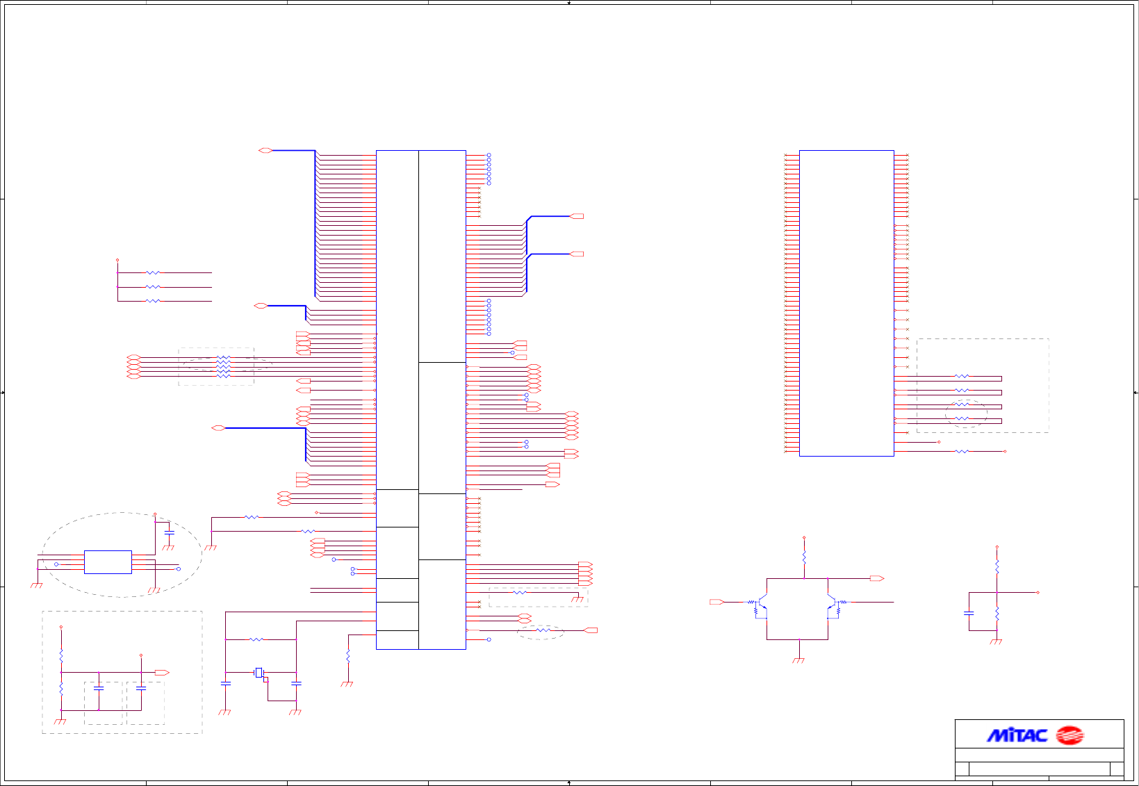
1
1
2
2
3
3
4
4
5
5
6
6
7
7
8
8
A A
B B
C C
D D
M6
MEMORY
MEMORY
INTERFACE
GPIO [13:0:] have internal pull-down
GPIO[7] - VGA disable : default position is 0 (i.e. VGA
enable)
GPIO[8] - ID disable : left open in normal operationGPIO[1:0] - AGP skew straps : allow for the adjustment
of the phase between AGP 1X CLK and PCICLK.
GPIO[3:2] - X1CLK_skew straps : allow for the
adjustment of the phase between X1CLK and
X2CLK.
GPIO[6:4] - Bus configuration straps : This straps are
controlling the bus type, the clock PLL select and the IDSEL.
Default is [000] - AGP 4X.
GPIO[13:11] - ROMIDCFG Straps : If the graphic subsystem
has no ROM attached, these straps serve for controlling the
chip ID.
ZV_LCDDATA [23:0:] have internal pull-down
ZV_LCDDCNTL [3:0:] have internal pull-down
GPIO[9] - External I2C : Data
GPIO[10] - External I2C : CLK
GPIO [10:9] for external
ROM or capture use.
8M DDR use R586, R590(M6-M)
16M DDR use R586, R590, R585, R589(M6-D)
DIGON->Controls Panel Digital Power On/Off
BLONb->Control Backlight On/Off
DAC2
ZV PORT/ EXT TMDS/ GPIO/
ROM
Internal DAC reference
LVDS
AGP4X
Place near MCH
TMDS
DVIDDCCLK & DVIDDCDATA
have internal pull-down
AGP2X
CRT2DDCCLK & CRT2DDCDATA
have internal pull-down
ATI Advice.
DAC1
Place near AGP
CLK SSC PCI/AGP
Special output pin for Apple
monitor
Pin has internal pulldown for default of VDDR 3.3V
Connect to VDDC(1.8V) for VDDR 2.5V
R01
R01
R01
R01
411671200001 02
VGA-M6(1/2)
Custom
10 22Friday, December 28, 2001
Title
Size Document
Number
Rev
Date: Sheet of
ZV_UV6
ZV_SYNC
AGP_AD0
-AGP_CBE3
AGP_SBA0
AGP_AD24
AGP_AD13
ZV_UV2
ZV_UV4
ZV_Y0
AGP_AD[0..31]
-M6_TRDY
AGP_AD17
ZV_UV3
ZV_Y1
-M6_SUS_STAT
LCD_ID0
-M6_FRAME
AGP_AD12
ZV_Y7
ZV_Y6
TX2OUT1+
TX2OUT2-
TXOUT0+-AGP_IRDY
-PCIRST
AGP_AD16
AGP_AD31
-AGP_CBE0
AGP_AD20
-AGP_CBE2
ZV_Y3
TXCLK+
TX2CLK+
-AGP_CBE[0..3]
-AGP_ADSTB0
AGP_ST1
ZV_UV[0..7]
-AGP_BUSY
ZV_UV1
TXOUT2+
AGP_ADSTB1 TX2OUT0-
-M6_SUS_STAT
AGP_AD7
AGP_AD25
AGP_AD19
AGP_SBA6
ZV_Y5
TX2OUT0+
AGP_SBSTB
-AGP_FRAME
-AGP_ADSTB1
ZV_PCLK
LCD_ID1
AGP_AD23
TXOUT2-
-AGP_RBF
AGP_AD2
AGP_AD21
-AGP_CBE1
AGP_AD10
ZV_Y2
66M_AGP
-M6_STOP
-M6_IRDY
AGP_AD9
AGP_AD6
AGP_AD18
AGP_SBA7
ZV_Y4
AGP_SBA4
AGP_AD28
AGP_SBA[0..7]
-AGP_REQ
-AGP_GNT
-STP_AGP
AGP_AD11
AGP_AD1
AGP_SBA2
AGP_PAR
TXOUT0-
AGP_ST2
ZV_HREF
AGP_AD8
AGP_AD5
AGP_AD4
ZV_UV5
TXCLK-
ENPVDD
-M6_DEVSEL
AGP_AD26
AGP_AD22
AGP_SBA3
-AGP_DEVSEL
-AGP_STOP
LCD_ID2
AGP_SBA5
AGP_AD3
TX2OUT1-
TX2CLK-
-AGP_TRDY
AGP_ST0
AGP_VREF
AGP_AD29
AGP_AD14
AGP_SBA1
AGP_AD15
ZV_UV7
TXOUT1-
TXOUT1+
AGP_ADSTB0
TX2OUT2+
-PCI_INTA
-AGP_SBSTB
ZV_Y[0..7]
-STP_AGP
-AGP_BUSY
AGP_AD30
AGP_AD27
ZV_UV0
SSOUT
SSIN
SSOUT
SSIN
-ENABKL
-ENABKL
-AGP_SERR
+1.8VS
+AGP_MEM_REF
VDDR_MEM2.5
+AGP_MEM_REF
AGP_VREF
AGP_VREF
+3VS
+1.5VS
+3VS
+5VS
C559
18P
25V
10%
0603D
12
R20
1K
0603
1%
12
R11
1K
0603
12
C556
18P
25V
10%
0603D
12
R19 4.7K 0603
1 2
R25
1K
0603
1%
12
R14 499 0603 1%
1 2
C78
0.1U
50V
0603
12
R573 0_DFS 0603
1 2
R572 0 0603
1 2
C60
0.01U
0603
12
U516B
MOBILITY-M6
BGA420_64_1MM
A26
B25
A25
A24
B23
A23
C22
B22
C21
B21
A21
D20
C20
B20
A20
C19
B18
A18
C17
B17
A17
D16
C16
B16
B15
A15
D14
C14
B14
A14
D13
C13
B1
C1
C2
D1
D2
E1
E2
F1
G2
G3
H1
H2
H3
J1
J2
J3
L1
L2
L3
L4
M1
M2
M3
N1
N4
P1
P2
P3
P4
R1
R2
R3
B13
A13
C12
B12
A12
D11
C11
B11
A11
C10
B10
A10
D9
C9
A22
D21
A16
C15
F2
G1
N2
N3
A19
B19
D18
C18
J4
K1
K2
K3
A9
C8
D8
B9
B8
A8
Y3
A6
A7
B6
B7
A4
A5
B4
B5
B3
T2
T1
DQ0
DQ1
DQ2
DQ3
DQ4
DQ5
DQ6
DQ7
DQ8
DQ9
DQ10
DQ11
DQ12
DQ13
DQ14
DQ15
DQ16
DQ17
DQ18
DQ19
DQ20
DQ21
DQ22
DQ23
DQ24
DQ25
DQ26
DQ27
DQ28
DQ29
DQ30
DQ31
DQ32
DQ33
DQ34
DQ35
DQ36
DQ37
DQ38
DQ39
DQ40
DQ41
DQ42
DQ43
DQ44
DQ45
DQ46
DQ47
DQ48
DQ49
DQ50
DQ51
DQ52
DQ53
DQ54
DQ55
DQ56
DQ57
DQ58
DQ59
DQ60
DQ61
DQ62
DQ63
MA0
MA1
MA2
MA3
MA4
MA5
MA6
MA7
MA8
MA9
MA10
MA11
MA12
MA13
DQM#0
DQM#1
DQM#2
DQM#3
DQM#4
DQM#5
DQM#6
DQM#7
QS0
QS1
QS2
QS3
QS4
QS5
QS6
QS7
RAS#
CAS#
WE#
CS#0
CS#1
CKE
ROMCS#
CLK0
CLK0_IN
CLK0#
CLK0#_IN
CLK1
CLK1_IN
CLK1#
CLK1#_IN
CLKFB
VREF
MEMVMODE
R581 47 0603
1 2
R534
1M
0603D
1 2
R546 20K 0603
1 2
TP514
1
TP521
1
TP516
1
U516A
MOBILITY-M6
BGA420_64_1MM
D24
C26
D25
D26
E23
E25
E24
E26
F26
G23
G25
G24
G26
H24
H26
H25
L23
L26
L24
M26
M24
N25
M25
N26
P23
P26
P24
R25
R24
R26
T23
T25
F23
J25
L25
N23
AA26
AA23
AA25
Y24
J23
J24
J26
K24
K26
K25
AA24
W24
AB25
AB26
W26
F25
P25
V25
W25
V24
V26
V23
U26
U24
T26
T24
Y26
Y23
Y25
U25
F24
N24
B26
C25
AE16
AF16
AF15
AF14
AE14
AF13
AF6
AF7
AE6
AE7
AF25
AF26
AC6
Y2
Y1
W3
W2
W1
V4
V3
V2
V1
U3
U2
U1
T4
T3
AA4
AB1
AB2
AB3
AB4
AC1
AC2
AC3
AD1
AD2
AD3
AE1
AE2
AF1
AF2
AF3
AE3
AF4
AE4
AD4
AF5
AE5
AD5
AC5
Y4
AA1
AA2
AA3
AC8
AD8
AC9
AD9
AE8
AF8
AC10
AD10
AE9
AF9
AD11
AC11
AE11
AF11
AD12
AC12
AD13
AE13
AE12
AF12
AD7
AD6
AC7
AB10
AB9
AE19
AF19
AE20
AF20
AE21
AF21
AE18
AF18
AD20
AC20
AD21
AF24
AF23
AF22
AE24
AE23
AE22
AD24
AD25
AC26
AC25
AE25
AC22
AD0
AD1
AD2
AD3
AD4
AD5
AD6
AD7
AD8
AD9
AD10
AD11
AD12
AD13
AD14
AD15
AD16
AD17
AD18
AD19
AD20
AD21
AD22
AD23
AD24
AD25
AD26
AD27
AD28
AD29
AD30
AD31
C/BE#0
C/BE#1
C/BE#2
C/BE#3
PCICLK
RST#
REQ#
GNT#
PAR
STOP#
DEVSEL#
TRDY#
IRDY#
FRAME#
INTA#
SERR#
STP_AGP#
AGP_BUSY#
RBF#
AD_STB0
AD_STB1
SB_STB
SBA0
SBA1
SBA2
SBA3
SBA4
SBA5
SBA6
SBA7
ST0
ST1
ST2
SB_STB#
ADSTRB0#
ADSTRB1#
AGPREF
AGPTEST
R2SET
C_R
Y_G
COMP_B
H2SYNC
V2SYNC
CRT2DDCCLK
CRT2DDCDATA
SSIN
SSOUT
XTALIN
XTALOUT
TESTEN
GPIO0
GPIO1
GPIO2
GPIO3
GPIO4
GPIO5
GPIO6
GPIO7
GPIO8
GPIO9
GPIO10
GPIO11
GPIO12
GPIO13
ZV_LCDDATA0
ZV_LCDDATA1
ZV_LCDDATA2
ZV_LCDDATA3
ZV_LCDDATA4
ZV_LCDDATA5
ZV_LCDDATA6
ZV_LCDDATA7
ZV_LCDDATA8
ZV_LCDDATA9
ZV_LCDDATA10
ZV_LCDDATA11
ZV_LCDDATA12
ZV_LCDDATA13
ZV_LCDDATA14
ZV_LCDDATA15
ZV_LCDDATA16
ZV_LCDDATA17
ZV_LCDDATA18
ZV_LCDDATA19
ZV_LCDDATA20
ZV_LCDDATA21
ZV_LCDDATA22
ZV_LCDDATA23
ZV_LCDCNTL0
ZV_LCDCNTL1
ZV_LCDCNTL2
ZV_LCDCNTL3
TXOUT_L0N
TXOUT_L0P
TXOUT_L1N
TXOUT_L1P
TXOUT_L2N
TXOUT_L2P
TXOUT_L3N
TXOUT_L3P
TXCLK_LN
TXCLK_LP
TXOUT_U0N
TXOUT_U0P
TXOUT_U1N
TXOUT_U1P
TXOUT_U2N
TXOUT_U2P
TXOUT_U3N
TXOUT_U3P
TXCLK_UN
TXCLK_UP
LTGIO0
LTGIO1
LTGIO2
DIGON
BLON#
TX0M
TX0P
TX1M
TX1P
TX2M
TX2P
TXCM
TXCP
DVIDDCCLK
DVIDDCDATA
HPD
R
G
B
HSYNC
VSYNC
RSET
MONID0
MONID1
VGADDCDATA
VGADDCCLK
SUS_STAT#
AUXWIN
TP515
1
R35
1K
0603
1%
1 2
R33
1K
0603
1%
1 2
R568 0_DFS 0603
1 2
X500
27MHZ
1 3
2
4
R564 0_DFS 0603
1 2
TP529
1
R538 20K 0603
1 2
TP520
1
R545 20K 0603
1 2
TP519
1
U503
P2040B
SO8
1
2
3
4 5
6
7
8
CLKIN
MRA
SR1
VSS SSON
MODOUT
SR0
VDD
TP511 1
C76
0.1U
50V
0603
12
C574
0.1U
50V
0603
12
TP506
1
TP510 1
TP512
1
TP503
1
TP502
1
TP513
1
TP10
1
TP13
1
TP508
1
TP504
1
TP11
1TP15
1
TP554
1TP12
1
TP505 1
TP509 1
TP14
1
TP507
1
R539 0_DFS 0603
1 2
Q12
DTC144WK
1
2
3
Q3
DTC144WK
1
2
3
R585 33 0603
1 2
R22
10K
0603
12
R586 33 0603
1 2
R590 33 0603
1 2
R533 845 0603
1 2
R567 0 0603
1 2
R589 33 0603
1 2
VSYNC (12)
HSYNC (12)
GREEN (12)
TXOUT0+ (12)
TX2OUT0- (12)
AGP_ST0(7,14)
ZV_UV[0..7] (15)
BLUE (12)
AGP_SBA[0..7](7)
AGP_ADSTB0(7,14)
TXOUT0- (12)
66M_AGP(8)
-AGP_ADSTB0(7,14)
LCD_ID2 (12)
-SUS_STAT (13,18)
TXOUT2+ (12)
AGP_ADSTB1(7,14)
-AGP_STOP(7,14)
ZV_Y[0..7] (15)
-AGP_GNT(7,14)
TX2OUT0+ (12)
SDA (12)
-AGP_IRDY(7,14)
-AGP_ADSTB1(7,14)
LCD_ID1 (12)
TXCLK+ (12)
AGP_VREF (7)
ZV_SYNC (15)
LCD_ID0 (12)
TX2OUT2- (12)
SCL (12)
-AGP_TRDY(7,14)
-AGP_CBE[0..3](7)
ENPVDD (12)
AGP_AD[0..31](7)
CSYNC(22)
ZV_HREF (15)
TX2OUT1- (12)
-AGP_FRAME(7,14)
TV_COMP(22)
-PCIRST(7,13,16,18)
TXOUT2- (12)
TXCLK- (12)
TX2CLK- (12)
TV_LUMA(22)
ZV_PCLK (15)
TX2OUT1+ (12)
-AGP_DEVSEL(7,14)
TV_CRMA(22)
TXOUT1+ (12)
AGP_ST2(7,14)
TX2CLK+ (12)
RED (12)
TXOUT1- (12)
TX2OUT2+ (12)
AGP_ST1(7,14)
AGP_PAR(7)
-PCI_INTA(13,14,15)
-AGP_RBF(7,14)
AGP_SBSTB(7,14)
-AGP_SBSTB(7,14)
ENPBLT (22)
-ENABKL_MSK(13)
-AGP_SERR(14)
-AGP_REQ(7,14)
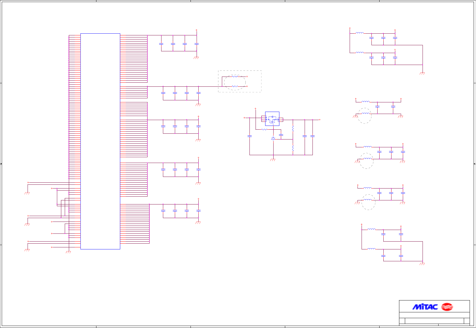
5
5
4
4
3
3
2
2
1
1
D D
C C
B B
A A
(LVDDR 40MA)
(TXVDDR 40MA)
(AVDD 90MA)
CORE
& I/O
POWER
1A
Select 3.3V or 2.5V to match
internal memory core VDD
PLACE CLOSE TO M6-M
PLACE CLOSE TO M6-M
PLACE CLOSE TO M6-M
PLACE CLOSE TO M6-M
PLACE CLOSE TO M6-M
02
R01
R01
R01
RO1
411671200001
VGA-M6(2/2)
11 22Friday, December 28, 2001
Title
Size Document
Number
Rev
Date: Sheet of
VDD_MCLK2.5
VDD_PNLIO1.8
+1.8VS
+1.8VS
VDD_PLL1.8
VDD_MEMPLL1.8
+1.8VS
VDD_DAC2.5
VDDR_MEM2.5
VDD_DAC1.8
VDD_PNLIO1.8
VDDR_MEM2.5
VDD_PLL1.8
VDD_MEMPLL1.8
VDD_DAC1.8
VDD_PNLPLL1.8
VDD_MCLK2.5
VDD_DAC2.5
VDDR_MEM2.5
+3V
VDD_PNLPLL1.8+1.8VS
VDD_MEMPLL1.8_GND
VDD_PNLPLL1.8_GND
VDD_PLL1.8_GND
VDD_MEMPLL1.8_GND
VDD_PNLPLL1.8_GND
+12VS
+1.8VS
VDD_PLL1.8_GND +1.5VS
+3VS
+3VS
VDDR_MEM2.5
C72
1U
0603
12
C67
22U
10V
1210
12
R588
4.7K_1%
0603
12
R587
4.99K
0603
1%
12
C49
22U
10V
1210
12
C59
22U
10V
1210
12
C61
22U
10V
1210
12
R694
0/NA
1210
1 2
R160
0
1210
1 2
C77
1U
0603
12
C68
1U
0603
12
C606
0.1U
50V
0603
12
C47
0.1U
50V
0603
12
C569
4.7U
0805
+80-20%
12
L6
120Z/100M
1608
1 2
L5
0_DFS
0603D_DFS
1 2
C37
0.1U
50V
0603
12
C50
0.1U
50V
0603
12
C79
4.7U
0805
+80-20%
12
U516C
MOBILITY-M6
BGA420_64_1MM
E5
C3
B2
A1
D4
T10
T11
T12
T13
T14
T15
T16
T17
K10
K11
K12
K13
K14
K15
K16
K17
L10
L11
L12
L13
L14
L15
L16
L17
M10
M11
M12
M13
M14
M15
M16
M17
N10
N11
N12
N13
N14
N15
N16
N17
P10
P11
P12
P13
P14
P15
P16
P17
R10
R11
R12
R13
R14
R15
R16
R17
U10
U11
U12
U13
U14
U15
U16
U17
C4
D3
E4
F5
D5
AE26
AD26
AC13
AD14
AB13
AC14
AE10
AF10
AC19
AD19
AD18
AD17
AC18
AE17
AF17
AD16
AD15
AC15
AC16
AE15
AD23
AD22
AC21
A2
A3
C5
AB11
H5
K5
M5
R5
U5
W5
AB8
AB14
AB7
AB17
AB19
W22
U22
R22
M22
K22
H22
E19
E17
E15
E12
E10
E8
AB12
E22
F22
G22
H23
J22
K23
L22
M23
N22
P22
R23
T22
U23
V22
W23
Y22
AA22
AB23
AB24
D23
C24
T5
U4
V5
W4
Y5
AA5
AC4
AB5
AB6
AB15
AB16
AB18
AB20
AB21
AB22
AC17
AC23
AC24
E6
E7
E9
E11
E13
E14
E16
E18
E20
E21
G5
H4
J5
K4
L5
M4
N5
P5
R4
D7
B24
F3
D6
C6
D15
D19
D22
G4
D10
C7
C23
D12
D17
E3
F4
VSS_0
VSS_1
VSS_2
VSS_3
VSS_4
VSS_5
VSS_6
VSS_7
VSS_8
VSS_9
VSS_10
VSS_11
VSS_12
VSS_13
VSS_14
VSS_15
VSS_16
VSS_17
VSS_18
VSS_19
VSS_20
VSS_21
VSS_22
VSS_23
VSS_24
VSS_25
VSS_26
VSS_27
VSS_28
VSS_29
VSS_30
VSS_31
VSS_32
VSS_33
VSS_34
VSS_35
VSS_36
VSS_37
VSS_38
VSS_39
VSS_40
VSS_41
VSS_42
VSS_43
VSS_44
VSS_45
VSS_46
VSS_47
VSS_48
VSS_49
VSS_50
VSS_51
VSS_52
VSS_53
VSS_54
VSS_55
VSS_56
VSS_57
VSS_58
VSS_59
VSS_60
VSS_61
VSS_62
VSS_63
VSS_64
VSS_65
VSS_66
VSS_67
VSS_68
VSS_69
VSS_70
VSS_71
VSS_72
VSS_73
PVDD
PVSS
LVDDR_0
LVDDR_1
LVSSR_0
LVSSR_1
LPVDD
LPVSS
TXVDDR_0
TXVDDR_1
TXVSSR_0
TXVSSR_1
TXVSSR_2
TPVDD
TPVSS
A2VDD
A2VDDQ
A2VSSN_0
A2VSSN_1
A2VSSQ
AVDD
AVSSN
AVSSQ
MPVDD
MPVSS
VDDRH
VDDC_0
VDDC_1
VDDC_2
VDDC_3
VDDC_4
VDDC_5
VDDC_6
VDDC_7
VDDC_8
VDDC_9
VDDC_10
VDDC_11
VDDC_12
VDDC_13
VDDC_14
VDDC_15
VDDC_16
VDDC_17
VDDC_18
VDDC_19
VDDC_20
VDDC_21
VDDC_22
VDDC_23
VDDC_24
VDDP_0
VDDP_1
VDDP_2
VDDP_3
VDDP_4
VDDP_5
VDDP_6
VDDP_7
VDDP_8
VDDP_9
VDDP_10
VDDP_11
VDDP_12
VDDP_13
VDDP_14
VDDP_15
VDDP_16
VDDP_17
VDDP_18
VDDP_19
VDDP_20
VDDR3_0
VDDR3_1
VDDR3_2
VDDR3_3
VDDR3_4
VDDR3_5
VDDR3_6
VDDR3_7
VDDR3_8
VDDR3_9
VDDR3_10
VDDR3_11
VDDR3_12
VDDR3_13
VDDR3_14
VDDR3_15
VDDR3_16
VDDR3_17
VDDR1_0
VDDR1_1
VDDR1_2
VDDR1_3
VDDR1_4
VDDR1_5
VDDR1_6
VDDR1_7
VDDR1_8
VDDR1_9
VDDR1_10
VDDR1_11
VDDR1_12
VDDR1_13
VDDR1_14
VDDR1_15
VDDR1_16
VDDR1_17
VDDR1_18
VDDR1_19
VDDQM_0
VDDQM_1
VDDQM_2
VDDQM_3
VDDQM_4
VDDQM_5
VDDQM_6
VDDQM_7
VDDM_0
VDDM_1
VDDM_2
VDDM_3
VDDM_4
VDDM_5
VDDM_6
L514
120Z/100M
1608
1 2
C53
0.1U
50V
0603
12
C52
0.1U
50V
0603
12
C613
10U
1206
12
C568
0.1U
50V
0603
12
R591
4.7K
0603
1 2
C43
0.1U
50V
0603
12
C560
0.1U
50V
0603
12
Q505
SCK431LCSK-.5
SOT23N
3 2
1
G
D
S
U505
AO4400
SO8
8
7
6
4
52
3
1
C610
4.7U
0805
+80-20%
12
L510
0_DFS
0603D_DFS
1 2
C75
0.1U
50V
0603
12
L506
120Z/100M
1608
1 2
C71
0.1U
50V
0603
12
L507
120Z/100M
1608
1 2
L4
120Z/100M
1608
1 2
C70
0.1U
50V
0603
12
C63
0.1U
50V
0603
12
C48
4.7U
0805
+80-20%
12
C611
470P
0603
1 2
C35
4.7U
0805
+80-20%
12
C604
0.1U
0603
12
C602
0.1U
50V
0603
12
C42
4.7U
0805
+80-20%
12
C64
0.1U
50V
0603
12
L515
0_DFS
0603D_DFS
1 2
C596
0.1U
50V
0603
12
L11
120Z/100M
1608
1 2
C561
4.7U
0805
+80-20%
12
L7
120Z/100M
1608
1 2
C605
0.1U
50V
0603
12
C51
0.1U
50V
0603
12
C608
10U
1206
12
C74
0.1U
50V
0603
12
C41
0.1U
50V
0603
12
C38
0.1U
50V
0603
12
C66
1U
0603
12
C73
22U
10V
1210
12
C44
1U
0603
12
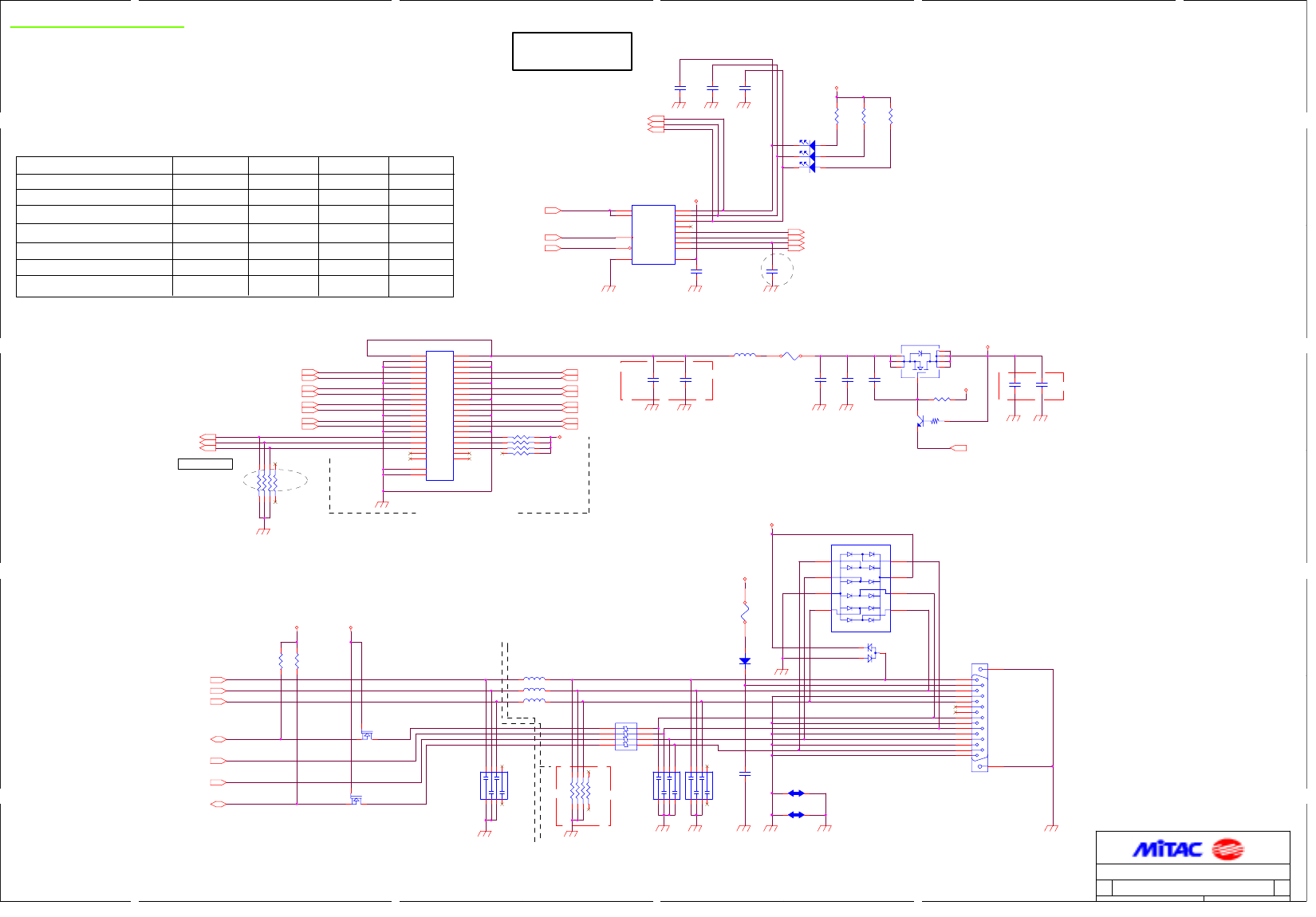
5
5
4
4
3
3
2
2
1
1
D D
C C
B B
A A
74VHC164
External VGA Connector
Close to VGA Connector
LCD & CRT INTERFACE
W/S=16/12/12/12/16 mils
GND_CRT15
GND_CRT15 GND_CRT15 GND_CRT15 GND_CRT15
D15 D13 D14
NUM CAP SCROLL
LED INDICATOR
GND_CRT15
DDC2B 1Amp
(40mil-60mil)
GND_CRT15
(NA D13,D14,D15,R157
,R683,R684 For LCD 15")
Close to VGA Connector
ǐ
#%##!" &$#
LCD CONNECTOR
as short as possible
S/W/W/S=12/6/6/12 mils
Layout Note:
Close to LCD Connector
CLOSE TO NDS 9410
LCD 14" 330mA,15"800mA
DISPLAY LCD_ID2 LCD_ID1 LCD_ID0
UNIPAC 0 0 1
HYUNDAI 0 1 0
HANNSTAR 0 1 1
Unipac(SXGA) 1 0 0
HannStar(SXGA) 1 0 1
HannStar(XGA)15"110
Sumsung(SXGA+)15" 1 1 1
LCD ID SELECT
R01
VIL--->2V
Internal 10K
R01
411671200001 02
LCD & CRT Interface
12 22Friday, December 28, 2001
Title
Size Document
Number
Rev
Date: Sheet of
-BATT_G
-H8_RESET
LED_CLK -BATT_R
LED_DATA
-AC_POWER
SDA
-BATT_LED
HSYNC
VSYNC
SCL
DDC2B
RED
GREEN
BLUE
-CAP
-NUM
-SCROLL
ENPVDD
TX2OUT0+
TX2OUT2-
TXCLK+
TXOUT2+
TXOUT0-
TX2OUT1+
TXOUT0+
LCDVCC
TX2CLK-
LCDVCC
TXCLK-
LCD_ID1
TXOUT1+
TX2OUT2+
TX2CLK+
TX2OUT0-
LCD_ID0
LCD_ID2
TXOUT1-
TX2OUT1-
TXOUT2-
+5VAS
+5VS
+5VS
+5VS
+5V
+3VS
+3VS
+3VS
+12VS
RP1
6.8K*4
1206
1
2
3
4
8
7
6
5
R684
470
0603
12
U500
PACDN006/NA SSOP8
1
2
3
4
8
7
6
5
D
S
Q501
2N7002
G
DS
J1
VGA
SUYIN
7535S-15G2T-05
1
9
2
10
3
11
4
12
5
13
6
14
7
15
8
17
16
U514
74VHC164
TSSOP14
1
2
8
9
3
4
5
6
10
11
12
13
7 14
A
B
CLK
CLR
QA
QB
QC
QD
QE
QF
QG
QH
GND VCC
D2
BAV99_NA
1
23
FA500
120OHM/100MHZ
1
2
3
4 5
6
7
8
C512
10U
10V
1206
12
D14 PG1102W
AK
CP501
22P*4
1206
1
2
3
4
8
7
6
5
F501
mircoSMDC110
12
CP500
22P*4
1206
1
2
3
4
8
7
6
5
CP506
22P*4
1206
1
2
3
4
8
7
6
5
D13 PG1102W
AK
R1
Q2
DTC144TKA
2
1
3
JL500
SHORT-SMT3
1 2
JL1
SHORT-SMT3
1 2
R543
4.7K
0603
12
L502120Z/100M 1608
1 2
L501120Z/100M 1608
1 2
R501 470K
0603
1 2
C501
10U_NA
10V
1206
12
C507
0.1U
50V
0603
12
R157
470
0603
12
D15 PG1102W
AK
L505120Z/100M 2012
1 2
R544
4.7K
0603
12
C1
1000P
0603
12
C714
0.1U
50V
0603
12
G
D
S
Q500 AO4400 SO8
8
7
6
4
5
2
3
1
C506
0.1U
50V
0603
12
C510
1000P
0603
12
R683
470
0603
12
C508
10U_NA
10V
1206
12
L500120Z/100M 1608
1 2
RP501
75*4
1206
1
2
3
4
8
7
6
5
D500
EC11FS2
AK
D
S
Q502
2N7002
G
DS
J2
MA/20PX2/ST
ACES
87216-4000
1
3
5
7
9
11
13
15
17
2
4
6
8
10
12
14
16
18
2019
GND1
GND2
21
23
25
27
29
22
24
26
28
30
31
33
35
37
39
32
34
36
38
40
F502
mircoSMDC110
12
RP520
47K*4
1206
1
2
3
4
8
7
6
5
C711
1U/NA
0603
12
C712
1U/NA
0603
12
C713
1U/NA
0603
12
C719
1U
0603
12
C503
0.1U
50V
0603
12
LED_DATA(19)
-H8_RESET(19)
LED_CLK(19)
RED(10)
HSYNC(10)
BLUE(10)
VSYNC(10)
SDA(10)
GREEN(10)
SCL(10)
-AC_POWER (22)
-BATT_R (22)
-BATT_G (22)
-BATT_LED (22)
-SCROLL(17,19) -NUM(17,19) -CAP(17,19)
LCD_ID0(10)
ENPVDD (10)
TX2OUT2+(10) TXOUT0- (10)
TXCLK+ (10)
TXOUT2-(10) TXOUT2+(10)
TXCLK- (10)
TX2OUT1- (10)
TX2CLK-(10)
TX2OUT2-(10)
LCD_ID1(10)
TX2OUT1+ (10)
TX2CLK+(10)
LCD_ID2(10)
TXOUT0+ (10)
TX2OUT0+(10)
TXOUT1+ (10)
TXOUT1- (10)
TX2OUT0-(10)
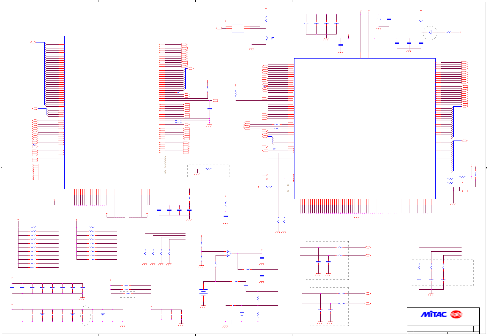
5
5
4
4
3
3
2
2
1
1
D D
C C
B B
A A
AC_SDIN1 FOR MDC.
CLOSE ICH2
AC_SDIN0 FOR Audio Codec.
ORNC7S32
Supply Voltage(Vcc) 2.0V to 6.0V
W/S=6/12 mils
W/S=6/12 mils
Close to ICH2
Close to ICH2
For Vccsus & vccusb pin
2V~3.6V 4uA
AC_SDOUT PULL HIGH FOR SAFEMODE.
RTC BATTERY CONN.
RTC CIRCUITRY
NO MDC NEED PULL DOWN 10K
ICN2 INTERNAL PULL UP
(2.0V~3.3V)
Tr>10mS
R01
R01
411671200001 02
ICH2
13 22Friday, December 28, 2001
Title
Size Document
Number
Rev
Date: Sheet of
AD26
AD5
-HUB_STB
-H_INIT
-PCIRST
-IRDY
-DEVSEL
-CBE2
AD24
AD22
AD8
HUB_D5
HUB_STB
-H_IGNNE
-H_A20M
-SERR
PAR
AD18
AD16
AD12
HUB_D8
-CBE[0..3]
-STOP
AD13
HUB_D3
HUB_D0
IRQ14
-PME
-FRAME
AD21 HUB_D9
-PCI_INTD-CBE0
AD19
AD3
AD1
HUB_D7
-PCI_INTB
-RCIN
AD31
AD10
IRQ15
AD29
AD28
AD14
-PCI_GNT1
-SLP
AD25
AD11
H_INTR
-PCI_REQA
-TRDY
AD17
AD2
HUB_D6
HUB_D2
SERIRQ
-H_SMI
AD6
HUB_D1
-PCI_REQ1
-PCI_INTC
H_PWRGD
-PCI_INTA
ICH_A20GATE
H_NMI
PCICLK_ICH
-PERR
AD20
-PCI_GNT0
-LOCK
AD30
AD27
AD0
-H_FERR
-CBE3
AD23
AD15
AD7
AD4
-PCI_REQ0
-H_STPCLK
-CBE1
AD9
HUB_D10
HUB_D4
PDD8
PDD4
USBP2+
-LFRAME
RTC_X2
-RTC_RST
ACSDIN
ACBITCLK
SMBDATA
-RSMRST
-SUSC
-PCIRST_MSK
SDD11
SDD8
PDD13
-PWRBTN
SDD12
SDD2
USBCLK_ICH
PWROK
SDD5
PDD9
LAD0
-THRM
PDD3
LAD1
MSDIN
PDD2
-INTRUDER
SDD[0..15]
66M_ICH
USBCLK_ICH
SDD10
SDD3
SDD1
PDD0
-SUS_STAT
PDD15
PDD[0..15]
-USBOC2
SBSPKR
RTC_X1
-SUSB
SDD14
SDD6
SDD0
PDD10
PDD7
PDD1
PDD14
PDD6
USBP3+
SDD15
SDD4
PDD12
USBP3-
USBP2-
-ACRST
14M_ICH
RTC_VBIAS
SDD13
SDD9
PDD11
PDD5
LAD2
ACSDOUT
66M_ICH
SMBCLK
14M_ICH
SDD7
-USBOC0
-LDRQ
-WAKE_UP
LAD3
-PCIRST_MSK
-PCIRST
SUS_CLK32K
-GATE1394
-1394WR
USBP2_2+
USBP2_2-
USBP0+
USBP0-
USBP2-
USBP2+
USBP0+
USBP1+
USBP0-
USBP1-
-PCI_REQ2
-PCI_REQ3
-PCI_REQ4
-PCI_REQ5
-PCI_GNT2
-PCI_GNT5
-PCI_GNT4
-PCI_GNT3
+5VS_ICHREF
VRMPWRGD
DRAMENA
USBP0_0-
USBP0_0+
-CDROM_PWRON
-HDD_PWRON
-PCI_GNTA
-PCI_INTE
-PCI_INTF
-PCI_INTG
-RSMRST
-SMB_ALERT
-PCI_INTH
-SCI
-EXTSMI
GPIO6
GPI7
GPI13
-ENABKL_MSK
-HDD_RST
SPK_OFF
DRAMENA
GPI7
-CDROM_RST
-ENABKL_MSK
GPIO6
-HDD_RST
-PCIRST
-CDROM_RST
-EXTSMI
SPK_OFF
-SCI
-GATE1394
-1394WR
GPI13
-PCIRST_MSK
-RCIN
ICH_A20GATE
-THRM
ACSDOUT
-SMB_ALERT
SMBDATA
-WAKE_UP
SMBCLK
RTC_VBIAS
RTC_X2
RTC_X1
-RTC_RST
ACSYNC
MSDIN
USBP3+
USBP1-
USBP1+
USBP3-
-PME
-RSMRST
+5V
VCC_RTC
CPU_CORE
+3VS
+1.8VS
+1.8V_ICH
+3V
+1.8VS
+3VS
+5VS
+3VS
+1.8VS
+3VS
+3VS
VCC_RTC
+3VS
VCC_RTC
+3V
+3V_ICH
+3V_ICH
+3V_ICH
+3V_ICH
+3V_ICH
+3V_ICH
+5VA
+3V_ICH
R155 10K
0603D
1 2
R153 10K
0603D
1 2
R159
1M
0603
1%
12
R689
330K
0603
12
C153
4.7U
0805
+80-20%
12
C680
47P
0603
12
C673
0.1U
50V
0603
12
C683
0.1U
50V
0603
12
C677
0.1U
50V
0603
12
C652
1U
0603
12
R96 10K 0603
1 2
C650
1U
0603
12
R1
Q15
DTC144TKA
2
1
3
TP548 1
C212
12P 0603
5%
1 2
R69 1K0603
1 2
R86 10K 0603
1 2
TP549 1
R152 10K0603 1 2
R87 10K 0603
1 2
R11010K/NA0603
1 2
C155
0.1U
50V
0603
12
R651 10K0603 1 2
C195
0.1U
50V
0603
12
R144 10K 0603
1 2
TP39 1
C128
0.1U
50V
0603
12
C129
0.1U
50V
0603
12
R128
10K
0603
12
C127
0.1U
50V
0603
12
R94 10K 0603
1 2
R656 10K 0603
1 2
R97 10K 0603
1 2
TP546
1
C143
47P
0603
12
C695
0.1U/NA
50V
0603
12
C679
0.1U
50V
0603
12
C177
0.1U
50V
0603D
12
C211
12P 0603
5%
1 2
C699
0.1U
50V
0603
12
C130
0.1U
50V
0603
12
C170
0.1U
50V
0603
12
C690
0.1U
50V
0603
12
R661 10K
0603D
1 2
R136 10K 0603D
1 2
R633
1K 0603D
1 2 C698
10P
0603D
12
U16
NC7S32
SOT70
1
2
3
5
4A
B
GND
VCC
Y
C651
0.047U
0603D
12
R75
10K/NA
0603D
12
R77
15
0603D
12
C150
0.1U
50V
0603
12
C126
0.1U
50V
0603
12
R100
10K
0603
12
R674 22 0603
1 2
R147 22 0603
1 2
C140
0.1U
50V
0603
12
R654
15
0603D
12
BT1
BH-800.1K
12
R146
10M
0603D
12
R89
10K/NA
0603D
12
R93 10K 0603
1 2
R145
10M
0603D
12
C147
0.1U
50V
0603
12
R1508.2K/NA
0603D
1 2
C682
4.7U
0805
+80-20%
12
R662
15
0603D
12
X3
32.768KHZ
CM200
14
R82
40.2
0603
1%
1 2
C144
0.1U
50V
0603
12
R118 8.2K 0603
1 2
U17A
82801
BGA288_36_36
AA4
AB4
Y4
W5
W4
Y5
AB3
AA5
AB5
Y3
W6
W3
Y6
Y2
AA6
Y1
V2
AA8
V1
AB8
U4
W9
U3
Y9
U2
AB9
U1
W10
T4
Y10
T3
AA10
AA3
AB6
Y8
AA9
AB7
V3
W8
V4
W1
W2
AA15
AA7
W7
Y7
Y15
M3
L2
W11
N3
N2
N1
AA11
Y14
W14
AB15
A15
D14
C14
L1
B14
A14
AB14
AA14
D11
A12
R22
A11
C12
C11
B11
B12
C10
B13
C13
A13
A4
B5
A5
B6
B7
A8
B8
A9
C8
C6
C7
C5
A6
A7
A3
B4
P1
P2
P3
N4
F21
C16
N20
P22
N19
N21
R2
R3
T1
AB10
P4
L3
M2
M1
R4
T2
R1
L4
G2
G1
H1
F3
F2
F1
G3
H2
R5
T5
U5
V5
V6
V7
V8
R18
P18
J18
H18
G18
F18
E18
E17
E16
E15
E14
F5
G5
T18
U18
V17
V18
D2
E5
P5
V9
K19
L19
D10
H5
J5
V14
V15
V16
AD0
AD1
AD2
AD3
AD4
AD5
AD6
AD7
AD8
AD9
AD10
AD11
AD12
AD13
AD14
AD15
AD16
AD17
AD18
AD19
AD20
AD21
AD22
AD23
AD24
AD25
AD26
AD27
AD28
AD29
AD30
AD31
C/BE0#
C/BE1#
C/BE2#
C/BE3#
DEVSEL#
FRAME#
IRDY#
TRDY#
STOP#
PAR
PCIRST#
PLOCK#
SERR#
PERR#
PME#
REQA#/GPI0
GNTN#/GPIO16
PCICLK
GPI02/PIRQE#
GPI03/PIRQF#
GPIO4/PIRQG#
GPIO7
GPIO8
GPIO12
GPIO13
GPIO18
GPIO19
GPIO20
GPIO21
GPIO22
GPIO23
GPIO27
GPIO28
A20M#
CPUSLPA#
FERR#
IGNNE#
INIT#
INTR
NMI
SMI#
STPCLK#
RCIN#
A20GATE
CPUPWRGD
HL0
HL1
HL2
HL3
HL4
HL5
HL6
HL7
HL8
HL9
HL10
HL11
HL_STB
HL_STB#
HLCOMP
HUBREF
PIRQA#
PIRQB#
PIRQC#
PIRQD#
IRQ14
IRQ15
APICCLK
APICD0
APICD1
SERIRQ
REQ0#
REQ1#
REQ2#
REQ3#
REQ4#
REQB#GPIO1/REQ#5
GNT0#
GNT1#
GNT2#
GNT3#
GNT4#
GNTB#/GPIO17/GNT5#
LAN_RXD0G2
LAN_RXD0G3
LAN_RXD0G4
LAN_TXD0
LAN_TXD1
LAN_TXD2
LAN_CLK
LAN_RSTSYNC
VCC3_3_0
VCC3_3_1
VCC3_3_2
VCC3_3_3
VCC3_3_4
VCC3_3_5
VCC3_3_6
VCC3_3_7
VCC3_3_8
VCC3_3_9
VCC3_3_10
VCC3_3_11
VCC3_3_12
VCC3_3_13
VCC3_3_14
VCC3_3_15
VCC3_3_16
VCC3_3_17
VCCPX1
VCCPX2
VCCPS2
VCCPS1
VCCUSB1
VCCUSB2
VCCA1_8
VCC1_8_0
VCC1_8_1
VCC1_8_2
VCC1_8_3
VCC1_8_4
VCC1_8_5
VCCSUS1_8_0
VCCSUS1_8_1
VCCSUS1_8_2
VCCSUS1_8_3
VCCSUS1_8_4
C136
47P
0603
12
C145
0.1U
50V
0603
12
R112 10K 0603
1 2
R111 10K 0603
1 2
R60510K/NA
0603
1 2
R131
15K
0603D
12
R130
15K
0603D
12
D509
BAV70LT1
SOT23N
1
23
D10
BAT54
13
C176
0.1U
50V
0603D
12
C703
0.1U
50V
0603
12
C706
0.1U
50V
0603
12
C685
0.1U
50V
0603D
12
R632
1K
0603D
12
R650
0_DFS
0603
12
R129 10K 0603
1 2
R126
15K
0603D
12
C208
4.7U
0805
+80-20%
12
C213
0.1U
50V
0603D
12
C138
10P
0603D
12
R101 10K 0603
1 2
C122
1U
0603
12
C178
0.1U
50V
0603D
12
C203
22P
0603
12
C197
22P
0603
12
R123 22 0603
1 2
R119 10K 0603D
1 2 C187
22P
0603
12
C681
1U
16V
0805C
12
R120 10K 0603D
1 2
R135 22 0603
1 2
R114 22 0603
1 2
C171
1U
16V
0805C
12
C678
10P
0603D
12
R125
15K
0603D
12
R634
8.2K 0603D
1 2
C205
22P
0603
12
C181
1U
0603D
12
R154
8.2K
0603D
1 2
R127 22 0603
1 2
R90 8.2K 0603
1 2
U17B
82801
BGA288_36_36
W15
V21
AA13
W16
AB18
R20
Y16
W21
AA17
R21
Y17
AA18
AA16
AB16
AB17
Y11
M4
T19
T20
T21
U22
T22
D4
M19
P20
V22
P19
R19
P21
Y22
W22
N22
Y12
W12
AB13
AB12
Y13
W13
AB11
AA12
W17
Y18
AB19
AA19
W18
Y19
AB20
AA20
W19
Y20
Y21
W20
K4
K3
J4
J3
A1
A10
A2
A21
A22
AA1
AA2
AA21
AA22
AB1
AB2
AB21
AB22
B1
B10
B2
B21
B22
B3
B9
C2
C3
C4
C9
D3
D5
D6
D7
D8
D9
E6
E7
E8
E9
J10
J11
J12
J13
J14
J9
K1
K10
K11
K12
K13
K14
K9
L10
L11
L12
L13
L14
L9
M10
M11
M12
M13
M14
M9
N10
N11
N12
N13
N14
N9
P10
P11
P12
E21
C15
E19
D15
F20
F19
E22
A16
D16
B16
G22
B18
F22
B17
G19
D17
G21
C17
G20
A17
H19
H22
J19
J22
K21
L20
M21
M22
L22
L21
K22
K20
J21
J20
H21
H20
D18
B19
D19
A20
C20
C21
D22
E20
D21
C22
D20
B20
C19
A19
C18
A18
U19
V20
B15
U20
P9
P14
P13
U21
D12
D13
V19
K2
M20
GPIO25
GPIO24
THRM#
SLP_S3#
SLP_S5#
PWROK
RSM_PWROK
PWRBTN#
RI#
RSMRST#
SUSSTAT#
SUSCLK#
SMBDATA
SMBCLK
SMBALERT#/GPIO11
GPIO6
PIRQH#/GPIO5
INTRUDER#
RTCRST#
VBIAS
RTCX1
RTCX2
CLK66
CLK14
CLK48
AC_RST#
AC_SYNC
AC_BITCLK
AC_SDOUT
AC_SDIN0
AC_SDIN1
SPKR
LAD0/FWH0
LAD1/FWH1
LAD2/FWH2
LAD3/FWH3
LDRQ0#
LDRQ1#
LFRAME#/FWH4
FS0/FWH5
USBP0_P
USBP0_N
USBP1_P
USBP1_N
USBP2_P
USBP2_N
USBP3_P
USBP3_N
OC0#
OC1#
OC2#
OC3#
EE_CS
EE_DIN
EE_DOUT
EE_SHCLK
VSS_0
VSS_1
VSS_2
VSS_3
VSS_4
VSS_5
VSS_6
VSS_7
VSS_8
VSS_9
VSS_10
VSS_11
VSS_12
VSS_13
VSS_14
VSS_15
VSS_16
VSS_17
VSS_18
VSS_19
VSS_20
VSS_21
VSS_22
VSS_23
VSS_24
VSS_25
VSS_26
VSS_27
VSS_28
VSS_29
VSS_30
VSS_31
VSS_32
VSS_33
VSS_34
VSS_35
VSS_36
VSS_37
VSS_38
VSS_39
VSS_40
VSS_41
VSS_42
VSS_43
VSS_44
VSS_45
VSS_46
VSS_47
VSS_48
VSS_49
VSS_50
VSS_51
VSS_52
VSS_53
VSS_54
VSS_55
VSS_56
VSS_57
VSS_58
VSS_59
VSS_60
VSS_61
VSS_62
VSS_63
VSS_64
VSS_65
VSS_66
VSS_67
PDCS1#
SDCS1#
PDCS3#
SDCS3#
PDA0
PDA1
PDA2
SDA0
SDA1
SDA2
PDDREQ
SDDREQ
PDDACK#
SDDACK#
PDIOR#
SDIOR#
PDIOW#
SDIOW#
PIORDY
SIORDY
PDD0
PDD1
PDD2
PDD3
PDD4
PDD5
PDD6
PDD7
PDD8
PDD9
PDD10
PDD11
PDD12
PDD13
PDD14
PDD15
SDD0
SDD1
SDD2
SDD3
SDD4
SDD5
SDD6
SDD7
SDD8
SDD9
SDD10
SDD11
SDD12
SDD13
SDD14
SDD15
SMLINK0
SMLINK1
VRMPWRGD
BATLOW/TP0
VSS_70
VSS_69
VSS_68
VCCRTC
VCC_CPU1
VCC_CPU2
V5REF_SUS
V5REF1
V5REF2
C137
0.1U
50V
0603
12
R99 10K 0603
1 2
R108 8.2K 0603
1 2
R107 8.2K 0603
1 2
R7410K/NA 0603
1 2
D16
BAT54
13
R117 8.2K 0603
1 2
C131
4.7U
0805
+80-20%
12
R158
4.7K
0603
12
C125
4.7U
0805
+80-20%
12
PDA0 (14)
SBSPKR(17)
-SCS3 (14)
-LFRAME(18)
-SUSC(19,22)
66M_ICH(8) 14M_ICH(8)
-SUSB(15,19,22)
-PCS3 (14)
-LDRQ(18)
PWROK(19)
USBCLK_ICH(8)
SMBCLK(8,9)
SDD[0..15] (14)
-PCS1 (14)
-THRM(19)
-SCS1 (14)
LAD[0..3](18)
SMBDATA(8,9)
ACSDIN(17)
-USBOC0(22)
-ACRST(16,17)
MSDIN(16)
ACSDOUT(16,17) ACBITCLK(16,17)
-USBOC2(22)
PDD[0..15] (14)
SDA2 (14)
PDA2 (14)
PDA1 (14)
SDA1 (14)
SDA0 (14)
-PCI_GNT0 (14,15)
-PERR(14)
-PCIRST(7,10,16,18)
H_PWRGD (4)
AD[0..31](15,16)
-DEVSEL(14,15,16)
HUB_STB (7)
-PCI_INTB (14)
-PCI_GNT1 (14,16)
-STOP(14,15,16)
-SLP (4)
PCICLK_ICH(8)
-PCI_INTA (10,14,15)
HUB_D[0..10] (7)
PAR(15,16) -PCI_REQ0 (14,15)
-HUB_STB (7)
-PCI_REQ1 (14,16)
IRQ15 (14)
H_INTR (4)
SERIRQ (14,15,18)
-H_INIT (4)
-CBE[0..3](15,16)
-SERR(14,15,16)
-PCI_INTC (14,15)
-FRAME(14,15,16)
-TRDY(14,15,16)
-PME(15,16)
-H_STPCLK (4)
IRQ14 (14)
-IRDY(14,15,16)
-H_IGNNE (4)
-H_SMI (4)
H_NMI (4)
ICH_A20GATE (19)
-LOCK(14)
-H_A20M (4)
-PCI_INTD (14,16)
-H_FERR (4)
-PWRBTN(19)
-RCIN (19)
-GATE1394(15)
-1394WR(15)
-SUS_STAT(10,18)
HUB_VREF (7)
-PCIRST_N(15,16)
-SDACK (14)
SIORDY (14)
-SDIOR (14)
PIORDY (14)
-PDIOW (14)
SDREQ (14)
-PDIOR (14)
-WAKE_UP(19)
PDREQ (14)
-SDIOW (14)
-PDACK (14)
USBP2_2+ (22)
USBP2_2- (22)
DRAMENA(9)
USBP0_0- (22)
USBP0_0+ (22)
-CDROM_PWRON(14) -HDD_PWRON(14)
-PCI_REQ3 (14)
-PCI_REQ2 (14)
-PCI_REQ5 (14)
-PCI_REQ4 (14)
-PCI_GNT3 (14)
-PCI_GNT2 (14)
-PCI_GNT5 (14)
-PCI_GNT4 (14)
-PCI_REQA(14)
-PCI_INTE(14) -PCI_INTF(14) -PCI_INTG(14)
-SCI(19) -EXTSMI(19)
SPK_OFF(17)
-PCI_INTH(14)
VRMPWRGD (21)
-ENABKL_MSK(10)
ACSYNC(16,17)
-CDROM_RST(14)
-HDD_RST(14)
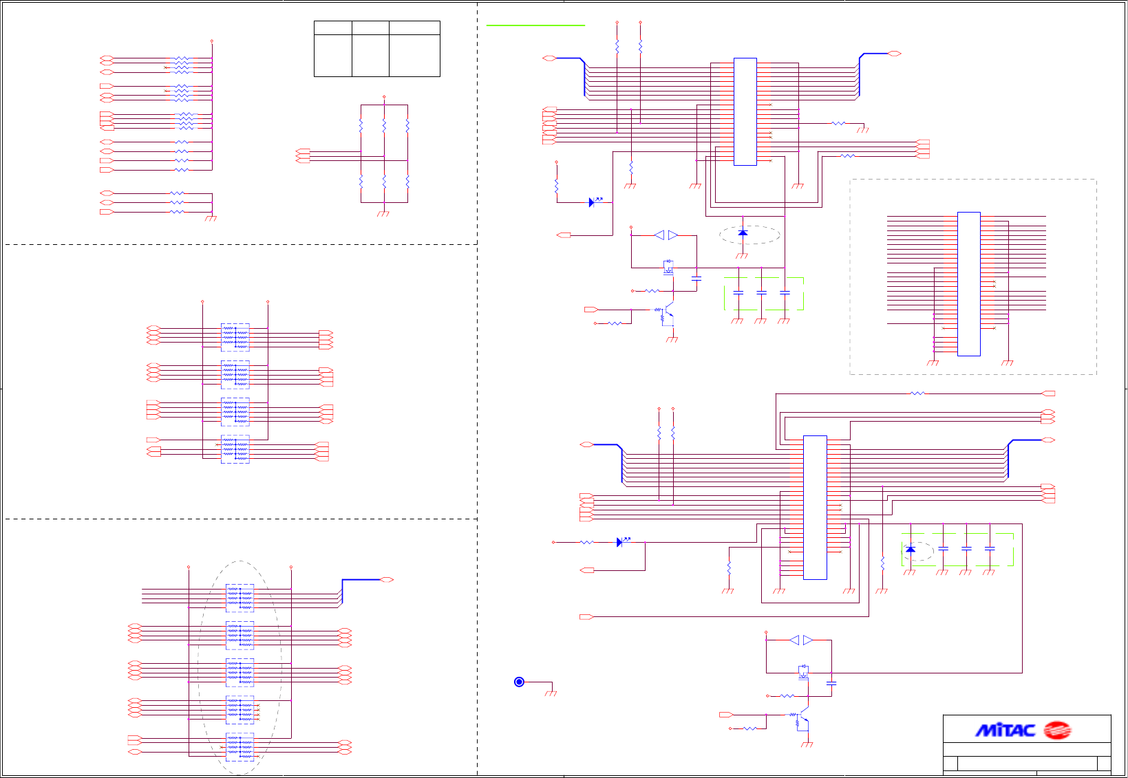
A
A
B
B
2 2
1 1
ENHANCED IDE
Primary EIDE Connector
R156 ,D12 For 15" Platform
To Audio Codec
Close to IDE Connector
W/S=16/12/12/16 mils
Secondary EIDE Connector
PLACE CLOSE TO VGA
AGP BUS
PCI BUS
ISA BUS
Close to IDE Connector
AGP_ST1 AGP_ST0 MCH STRAP
X
X
X
0
0
1
1
DDR
SDR
533MHZ
400MHZ
X
FOR 15" CD_ROM CONNECTOR
R682 ,D11 For 15" Platform
R01
R01
R01
411671200001 02
HDD, CDROM Connector & PULL-UP RESISTER
14 22Friday, December 28, 2001
C
Title
Size Document
Number
Rev
Date: Sheet of
PDD14
PDD10
PDD8
PDD15
PDD9
PDD[8..15]
-BRSTDRV1
PDD11
PDD12
PDD13
PDD[0..7]
PIORDY
PDREQ
-PDIOW
-PDACK
PDA0
PDA1
IRQ14
-PDIOR
PDA2
-PCS1
-PCS3
-SCS1
CABLE_SEL
SIORDY
CDROM_LEFT
SDA1
SDREQ
CDROM_COMM
-SDIOR
-SDIOW SDA2
SDA0
SDD[8..15]
PDD5
PDD2
PDD6
PDD3
PDD1
PDD4
PDD0
PDD7
-HDDACTP
-CDACTP
-SCS3
-SDACK
IRQ15
-BRSTDRV2
-HDD_RST
CDROM_RIGHT
-AGP_DEVSEL
-AGP_FRAME
-AGP_GNT
-AGP_IRDY
-AGP_PIPE
-AGP_TRDY
-AGP_STOP
-AGP_REQ
-AGP_RBF
AGP_SBSTB
AGP_ADSTB1
AGP_ADSTB0
-AGP_ADSTB0
-AGP_SBSTB
-AGP_ADSTB1
AGP_ST0
AGP_ST1
AGP_ST2
-AGP_WBF
-DEVSEL
-FRAME
-IRDY
-PERR
-LOCK
-SERR
-STOP
-TRDY
-PCI_REQA
-PCI_GNT0
-PCI_GNT1
-PCI_GNT2
-PCI_GNT3
-PCI_GNT4
-PCI_REQ0
-PCI_REQ1
-PCI_REQ2
-PCI_REQ3
-PCI_REQ4
-PCI_REQ5
-PCI_INTA
-PCI_INTB
-PCI_INTC SERIRQ
-PCI_GNT5
-PCI_INTD
-PCI_INTH
-PCI_INTG
-PCI_INTE
-PCI_INTF
SA0 SA4SA1
SA2
SA3
SA12
SA13
SA14
SA15
SA5
SA6
SA7
SA8
SA9
SA10
SA11
SA16
SA17
SA18
SA19
IRQ1
IRQ12 -IOR
SD1
SD3
SD0
SD2
SD5
SD7
SD4
SD6
-MCCS
SD[0..7]
-IOW
-AGP_SERR
-MEMR
-PCLKRUN
SDD[0..7]
SDD1
SDD5
SDD7
SDD2
SDD3
SDD4
SDD0
SDD6
-CDACTP
SDD5
-BRSTDRV2
-SDIOR
SDD12
SDD3
CDROMPWR
-SCS1
CABLE_SEL
SDD6
SDA1
SDD15
SDD11
CDROMPWR
CDROM_COMM
SIORDY
SDD7 SDD9
IRQ15
-SCS3
SDD10
CDROM_LEFT
-SDIOW
SDD8
CDROMPWR
SDA2
SDD4
SDD0
CDROM_RIGHT
CDROMPWR
SDD2
-SDACK
SDD1
SDA0
CDROMPWR
SDREQ
CDROMPWR
SDD14
SDD11
SDD14
SDD15
SDD12
SDD8
SDD13
SDD13
SDD10
SDD9
+3VS +3VS
+5VS
+3VS+3VS
+5VS
+1.5VS
+1.5VS
+3VS +3VS
+3VS+3VS
+12VS
+3VS
+5VS
+12VS
+5VS
+3VS
R580
10K
0603
1 2
Q14
DTC144WK
1
2
3
J10
FM/25PX2-R/A
C12441-X50XX
1
3
5
7
9
11
13
15
17
19
21
23
25
27
29
31
33
35
37
39
41
43
45
47
49
2
4
6
8
10
12
14
16
18
20
22
24
26
28
30
32
34
36
38
40
42
44
46
48
50
GND1
GND2
GND3
GND4
1
3
5
7
9
11
13
15
17
19
21
23
25
27
29
31
33
35
37
39
41
43
45
47
49
2
4
6
8
10
12
14
16
18
20
22
24
26
28
30
32
34
36
38
40
42
44
46
48
50
GND1
GND2
GND3
GND4
R561 6.8K 06035%
1 2
D
S
Q13
AO3400 G
D S
C201
0.1U
50V
0603
12
R562 6.8K 06035%
1 2
R24 6.8K 06035%
1 2
R576 6.8K 06035%
1 2
R137
1M0603
1 2
JO29
OPEN-SMT4
1 2
J23
FM/25PX2-R/A/NA
C12441-X50XX
1
3
5
7
9
11
13
15
17
19
21
23
25
27
29
31
33
35
37
39
41
43
45
47
49
2
4
6
8
10
12
14
16
18
20
22
24
26
28
30
32
34
36
38
40
42
44
46
48
50
GND1
GND2
GND3
GND4
1
3
5
7
9
11
13
15
17
19
21
23
25
27
29
31
33
35
37
39
41
43
45
47
49
2
4
6
8
10
12
14
16
18
20
22
24
26
28
30
32
34
36
38
40
42
44
46
48
50
GND1
GND2
GND3
GND4
R551
2K/NA
0603
12
R556
2K/NA
0603
12
D508
EC10QS04
A K
D513
EC10QS04
A K
R552
2K/NA
0603
12
C593
0.1U
50V
0603
12
Q504
DTC144WK
1
2
3
R577
1M0603
1 2
JO500
OPEN-SMT4
1 2
D
S
Q503
AO3400 G
D S
R91
10K
0603
12
R27 6.8K 06035% 12
D12 PG1102W
A K
R682
470
0603
1 2
R582
5.6K
0603
12
C184
0.1U
50V
0603
12
R550
6.8K
0603
5%
1 2
RP506 6.8K*4 1206
1
2
3
4
8
7
6
5
C182
4.7U
16V
1206
12
RP15
8.2K*8 1206
1
2
3
4
5 6
7
8
9
10
J14
MA/22PX2/ST
C16822-X44XX
1
3
5
7
9
11
13
15
17
19
21
23
25
27
29
31
33
35
37
39
41
43
2
4
6
8
10
12
14
16
18
20
22
24
26
28
30
32
34
36
38
40
42
44
1
3
5
7
9
11
13
15
17
19
21
23
25
27
29
31
33
35
37
39
41
43
2
4
6
8
10
12
14
16
18
20
22
24
26
28
30
32
34
36
38
40
42
44
RP18
8.2K*8 1206
1
2
3
4
5 6
7
8
9
10
C587
4.7U
16V
1206
12
R56
33
0603
1 2
RP17
8.2K*8 1206
1
2
3
4
5 6
7
8
9
10
RP16
8.2K*8 1206
1
2
3
4
5 6
7
8
9
10
R156
470
0603
1 2
D11 PG1102W
A K
R55
33
0603
1 2
R548
6.8K/NA
0603
5%
1 2
R79
470
0603
1 2
RP514
4.7K*8/NA 1206
1
2
3
4
5 6
7
8
9
10
R37
4.7K
0603
12
R557
6.8K
0603
5%
1 2
RP517
4.7K*8/NA 1206
1
2
3
4
5 6
7
8
9
10
RP513
4.7K*8/NA 1206
1
2
3
4
5 6
7
8
9
10
RP519
4.7K*8/NA 1206
1
2
3
4
5 6
7
8
9
10
RP516
4.7K*8/NA 1206
1
2
3
4
5 6
7
8
9
10
RP509 6.8K*4 1206
1
2
3
4
8
7
6
5
C198
0.1U
50V
0603
12
C591
0.1U
50V
0603
12
R36
10K
0603
12
C595
0.1U
50V
0603
12
RP507 6.8K*4 1206
1
2
3
4
8
7
6
5
MTG23
ID2.8/OD5.5
1
R84
4.7K
0603
12
R29
470/NA
0603
12
R578 6.8K 06035% 12
R71
5.6K
0603
12
R558 6.8K/NA 0603
5%
1 2
R138
10K
0603
1 2
PDD[8..15] (13)
PDA0(13)
PIORDY(13)
-PDIOR(13) -PDIOW(13)
PDA1(13) IRQ14(13)
PDD[0..7](13)
-PDACK(13)
PDREQ(13)
-PCS3 (13)
-PCS1 (13)
-HDD_RST (13)
PDA2 (13)
-SDACK (13)
SDD[8..15] (13)
CDROM_LEFT (17)
SDA2 (13)
CDROM_COMM (17)
-SDIOR (13)
SDA1(13)
-SCS1(13)
IRQ15(13)
SDD[0..7](13)
-SCS3(13)
SDREQ (13)
SDA0(13)
SIORDY(13)
-SDIOW(13)
-HDDACTP(17,19)
-CDACTP(17,19)
CDROM_RIGHT (17)
AGP_ADSTB1(7,10)
-AGP_PIPE(7)
-AGP_ADSTB0(7,10)
-AGP_WBF(7)
-AGP_SBSTB(7,10)
-AGP_ADSTB1(7,10)
-AGP_RBF(7,10)
-AGP_REQ(7,10)
AGP_ADSTB0(7,10)
AGP_SBSTB(7,10)
-AGP_IRDY(7,10)
-AGP_FRAME(7,10) -AGP_DEVSEL(7,10)
-AGP_GNT(7,10)
-AGP_STOP(7,10) -AGP_TRDY(7,10)
AGP_ST0(7,10) AGP_ST1(7,10) AGP_ST2(7,10)
-PCI_REQ1 (13,16)
-LOCK(13)
-PCI_GNT1 (13,16)
-SERR(13,15,16)
-IRDY(13,15,16)
-STOP(13,15,16)
-PERR(13)
-FRAME(13,15,16)
-TRDY(13,15,16) -PCI_REQ0 (13,15)
-PCI_REQA(13)
-PCI_GNT3 (13)
-PCI_REQ5 (13)
-PCI_GNT2 (13)
-PCI_REQ3 (13)
-PCI_REQ4 (13)
-PCI_GNT0 (13,15)
-PCI_GNT4 (13)
-PCI_REQ2 (13)
-DEVSEL(13,15,16)
-PCI_INTE (13)
-PCI_INTG (13)
-PCI_INTH (13)
SERIRQ (13,15,18)
-PCI_INTA(10,13,15) -PCI_INTB(13) -PCI_INTC(13,15)
-PCI_GNT5(13)
-PCI_INTD(13,16)
-PCI_INTF (13)
SA15(18)
SA16(18)
SA14(18)
SA19(18)
SA8 (18)
SA6 (18)
SA13(18)
IRQ1(18,19)
SD[0..7] (18,19)
SA7 (18)
SA4 (18)
-MCCS (18,19)
SA10 (18)
IRQ12(18,19)
SA17(18)
SA5 (18)SA2(18,19)
SA12(18)
SA9 (18)
SA3(18)
SA1(18)
SA11 (18)
SA0(18)
SA18(18)
-IOR (18,19)
-IOW (18,19)
-HDD_PWRON(13)
-CDROM_PWRON(13)
-AGP_SERR(10)
-MEMR(18)
-PCLKRUN(15,16)
-CDROM_RST (13)
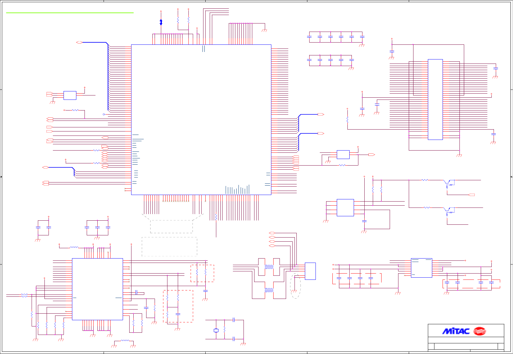
5
5
4
4
3
3
2
2
1
1
D D
C C
B B
A A
PCMCIA CONTROLLER & CARD BUS SCOKET
Close to TPS2211
Close to TPS2211
Card Bus Socket
Closed to PHY
Close to PHY
Close to PHY
The singals need to be
the same,length must
not execeed 4 inches
The length TPA+ and TPA- must
be the same.Also,TPB+ and TPB-
must be the same.Both pair
need to be as close the same
length as possible.
Meet 6.3K ohm.
Write Protect when high.
PCI4410 uBGA209
For PCMCIA Controller Decoupling
Close to PCI4410
(NA J21 For LCD 15")
R01
411671200001 02
PCMCIA/1394 Controller & Socket
15 22Friday, December 28, 2001
Title
Size Document
Number
Rev
Date: Sheet of
-CGNT
CSTSCHG
-CREQ
CAD30
-CCBE3
-CRST
CAD28
CAD25
CAD3
CAD7
CAD2
CAD11
CAD6
-CIRDY
CCLK
R2_A18
CAD12
-CBLOCK
CAD4
CAD15
CAD8
CAD18
-CCBE2
CAD9
CAD20
AD[0..31]
CAD31
VPPEN1
-VCCEN1
CAD19
CPAR
-CSERR
-VCCEN0
CAD17
CAD14
R2_D2
CAD5
CAD0
CAUDIO
-CSTOP
CAD21
-CCBE1
CAD29
CAD27
-CINT
CAD13
-CFRAME
CVS1
CAD22
R2_D14
CAD23
CAD16
CAD24
CAD26
CAD10
-CTRDY
VPPEN0
CVS2
CCLK
-CCBE0
-CDEVSEL
-CPERR
CAD1
-PME
-CBE[0..3]
AD19
ZV_Y[0..7]
R2_D2
PHY_D2
CAD28
SERIRQ
AD31
AD16
AD6
PHY_LPS
PHY_CTL1
PHY_D5
CAD19
AD22
-VCCEN0
R2_A18
CVS1
PHY_D6
CAUDIO
CAD21
-PCI_REQ0
AD27
AD2
-CRST
-CIRDY
-CINT
-CPERR
CSTSCHG
ZV_MCLK
CAD9
-DEVSEL
-IRDY
-PCI_GNT0
-CARDSPK
AD25
AD18
AD15
AD1
CPAR
PHY_D7
PHY_D3
CAD27
CAD18
PAR
-FRAME
-CTRDY
-CBE3
CAD15
CAD0
AD30
AD29
AD21
-VCCEN1
-CBE2
-CBLOCK
CAD26
AD26
AD3
CB_+3V
CAD30
CAD20
CAD17
CAD6
CAD4
CAD1
AD23
AD20
-CREQ
PHY_CTL0
PHY_D4
CAD23
AD28
CVS2
-CBE1
CAD11
CAD8
CAD3
PCICLK_CARD
-CSTOP
-PCI_INTC
CAD31
-STOP
AD14
AD10
AD9
AD8
AD5
AD4
VPPEN0
-CGNT
-CCBE2
PHY_D0
CAD25
CAD14
CAD13
CAD7
CAD5
AD17
AD13
-CFRAME
-CCBE3
-CCBE1
-CCBE0
PHY_CLK
-SERR
-CARD_RI
R2_D14
-CBE0
ZV_LRCLK
CAD16
CAD12
-CCLKRUN
-CCD2
PHY_LREQ
CAD29
CAD24
-TRDY
AD24
AD12
AD7
AD0
PHY_D1
ZV_DATA
CAD22
CAD10
AD19
AD11
-CBRST
VPPEN1
-CDEVSEL
-CSERR
-CCD1
PHY_LKON
CAD2
PHY_LREQ
PHY_D2
PHY_D4
PHY_D5
PHY_D7
PHY_D0
PHY_D6
PHY_D1
PHY_D3
PHY_XI
PHY_XO
PHY_CLK
PHY_LKON
SCLK
SDATA
SDATA
SCLK
-VCCEN0
-VCCEN1
-1394WR
TPA+
-1394WR
-PCI_INTA
PHY_LPS
-CCLKRUN
PHY_CTL0
PHY_CTL1
ZV_ACT
ZV_ACT
-PCLKRUN
TPB+
-CCD1
-CCD2
-CBRST
CB_+3V
CB_+3V
-CBRST
TPB+
TPA-
TPB-
ZV_Y1
ZV_UV5
ZV_UV2
ZV_UV4
ZV_Y6
ZV_HREF
ZV_SCLK1
ZV_UV6
ZV_UV[0..7]
ZV_UV7
ZV_Y7
ZV_UV0
ZV_PCLK
ZV_Y5
ZV_SYNC
ZV_Y2
ZV_Y0
ZV_UV1
ZV_Y4
ZV_Y3
ZV_UV3
PHY_XO
PHY_XI
TPB-
TPA-
TPA+
VCCA
+3V
VPPA
VCCA
VPPA
VPPA
+12V
+5V
+3V
+3VS
+3V
+3V
PHY_AGND
+3V
+3V
+3V
+5V
VCCA
+3V
+3V+5V
VCCA
+3V 1394AVDD
PHY_AGND
1394AVDD
+5VS
+3V
+3V
PHY_AGND
R43
47K
0603
1 2
JS8
SHORT-SMT3
1 2
C600
0.1U
50V
0603
12
C612
0.1U
50V
0603
12
R73
10
0603
1 2
U7
PCI4410GHK
BGA_GHK_209
U9
V9
W9
W8
V8
U8
R8
V7
P8
W6
R7
U6
V5
P7
R6
U5
N6
N3
N2
N1
M2
L5
L6
L3
K5
K3
K2
K1
J6
J3
J2
J1
W10
V10
P10
W11
U11
P11
R11
M6
U10
P9
W12
H1
H2
L1
P2
N5
R1
P6
R2
P5
R3
T1
L18
L14
L17
K18
K19
K15
K17
J19
J17
J15
H18
H17
G19
H14
G17
G18
G14
B15
C14
B14
A14
C13
B13
C12
A11
B11
R13
U14
W15
V15
R14
U15
W16
T19
R10
C11
C9
F9
E9
A8
C8
R17
N14
P15
P17
R18
N15
P18
N17
M17
M15
N19
N18
P19
V14
W14
C10
E10
B6
C6
F6
B5
E6
C5
A4
D1
E7E8
B7
C7
F7
E12
F8
A6
M3
V11
R12
G15
E19
D19
E3
F5
G6
E2
F3
F2
G5
F1
H6
G3
G2
H5
H3
J14
F19
F13
B12
L19
A9
V13
U13
U7
W4
P1
K6
P12
P13 F11
E13
B10
F14
E18
A10
F15
E17
A16
C15
F12
E14
F10
K14
F18
B8
E1
J5
M5
R9
R19
L15
H15
A15
E11
A5
P14
W5
V12
U12
M18
M19
H19
A12
G1
L2
P3
W7
W13
M14
J18
F17
A13
B9
A7
M1
V6
AD0
AD1
AD2
AD3
AD4
AD5
AD6
AD7
AD8
AD9
AD10
AD11
AD12
AD13
AD14
AD15
AD16
AD17
AD18
AD19
AD20
AD21
AD22
AD23
AD24
AD25
AD26
AD27
AD28
AD29
AD30
AD31
MFUNC0
MFUNC1
MFUNC2
MFUNC3
MFUNC4
MFUNC5
MFUNC6
PCLK
SPKROUT
RI_OUT/PME
SUSPEND
GNT
REQ
IDSEL
FRAME
IRDY
TRDY
DEVSEL
STOP
PERR
SERR
PAR
CAD0
CDA1
CDA2
CAD3
CAD4
CAD5
CAD6
CAD7
CAD8
CAD9
CAD10
CAD11
CAD12
CAD13
CAD14
CAD15
CAD16
CAD17
CAD18
CAD19
CAD20
CAD21
CAD22
CAD23
CAD24
CAD25
ZV_Y(0)
ZV_Y(1)
ZV_Y(2)
ZV_Y(3)
ZV_Y(4)
ZV_Y(5)
ZV_Y(6)
ZV_Y(7)
VCCI
CAD26
CAD27
CAD28
CAD29
CAD30
CAD31
ZV_UV(0)
ZV_UV(1)
ZV_UV(2)
ZV_UV(3)
ZV_UV(4)
ZV_UV(5)
ZV_UV(6)
ZV_UV(7)
ZV_PCLK
ZV_SDATA
ZV_LRCLI
ZV_MCLK
ZV_SCLK
ZV_VSYNC
ZV_YHREF
CAUDIO
CSTSCHG
PHY_DATA0
PHY_DATA1
PHY_DATA2
PHY_DATA3
PHY_DATA4
PHY_DATA5
PHY_DATA6
PHY_DATA7
VCCLPHY_LREQ
PHY_CLK
PHY_CTL(0)
PHY_CTL(1)
CREQ
LPS
LINKON
RST
G_RST
LEDA_SKT
CPAR
CBLOCK
CCLK
PHY_RSVD0
PHY_RSVD1
PHY_RSVD2
PHY_RSVD3
PHY_RSVD4
PHY_RSVD5
PHY_RSVD6
PHY_RSVD7
PHY_RSVD8
PHY_RSVD9
PHY_RSVD10
PHY_RSVD11
PHY_RSVD12
CC/BE0
CC/BE1
CC/BE2
CC/BE3
CCD1
CCD2
IBTA
INTB
C/BE0
C/BE1
C/BE2
C/BE3
RSVD
RSVP CVS1
CVS2
CSERR
CPERR
CSTOP
CINT
CGNT
CDEVSEL
CTRDY
CIRDY
CRST
CFRAME
CCLKRUN
CRSVD0
CRSVD1
CRSVD2
GND0
GND1
GND2
GND3
GND4
GND5
GND6
GND7
GND8
GND9
GND10
GND11
VPPD0
VPPD1
VCCD0
VCCD1
VCCCB0
VCCCB1
VCC0
VCC1
VCC2
VCC3
VCC4
VCC5
VCC6
VCC7
VCC8
VCC9
VCC10
VCCP0
VCCP1
C601
0.1U
50V
0603
12
Q4
DTC144WK
1
2
3
R85
1K
0603
12
C89
0.1U
50V
0603
12
C609
0.1U
50V
0603
12
C152
10P
0603
1 2
C199
270P
0603
10%
12
Q5
DTC144WK
1
2
3
C80
10P/NA
0603
10%
12
C134
10P
0603
1 2
C598
4.7U_NA
16V
1206
12
C124
0.1U
50V
0603
12
R38 22 0603
1 2
R81
1M_NA
0603
1 2
C161
0.1U
50V
0603
1 2
R124
4.99K
0603
1%
12
C594
0.1U
50V
0603
12
C607
4.7U_NA
16V
1206
12
C175
0.1U
50V
0603
12
C603
0.1U
50V
0603
12
C162
0.1U
50V
0603
12
R39
100
0603
1 2
C154
0.1U
50V
0603
12
R105
56
0603
12
R95
1K
0603
12
C151
0.1U
50V
0603
12
R41 4.7K 0603
1 2
U506
NC7S08/NA
SC70
1
2
3
5
4
A
B
GND
VCC
Y
C82
0.1U
50V
0603
12
R106
56
0603
12
C599
0.1U
50V
0603
12
R92
1K
0603
12
R80
1K
0603
1 2
R104
6.34K
0603
1%
12
R5930_DFS 0603
1 2
U14
TSB41AB1
PQFP64_0.5MM
1
2
3
4
5
6
7
8
9
10
11
12
13
14
15
16
17
18
19
20
21
22
23
24
25
26
27
28
29
30
31
33
34
35
36
37
38
39
40
41
42
43
44
45
46
47
48
49
50 51
52
53
54
55
56
57
58
59
60
61
62
63
64
32
LREQ
SYSCLK
CNA
CTL0
CTL1
D0
D1
D2
D3
D4
D5
D6
D7
PD
LPS
NC5
DGND0
DGND1
C/LKON
PC0
PC1
PC2
ISO
CPS
DVDD0
DVDD1
TESTM
SE
SM
AVDD0
AVDD1
AGND1
TPB-
TPB+
TPA-
TPA+
TPBIAS
AGND2
R0
R1
AVDD2
NC3
NC2
NC1
NC0
NC4
AGND3
AGND4
AGND5 AVDD3
AVDD4
RESET
FILTER0
FILTER1
PLLVDD
PLLGND0
PLLGND1
XI
XO
DVDD2
DVDD3
DGND2
DGND3
AGND0
R47
0/NA
0603
12
R579
47K
0603
12
C200
1U
0603
12
R103
56
0603
12
C98
10U_NA
10V
1206
12
U9
NM24C02N
SO8
1
2
3
4
5
6
7
8
A0
A1
A2
GND
SDA
SCLK
WC-
VCC
R83
10K
0603
12
R115
56
0603
12
C156
0.1U
50V
0603
12
C99
0.1U
50V
0603
12
R98
110K_NA
0603
12
J21
IEEE1394/4P
LINKTEK
AVR20-4XXX0X
1
2
3
4
GND1
GND2
1
2
3
4
GND1
GND2
R116
1M
0603
1%
12
R46
0_DFS
0603
12
C95
0.1U
50V
0603
12
C614
0.1U
50V
0603
12
C92
0.1U
50V
0603
12
C615
0.1U
50V
0603
12
L19
120Z/100M
2012
1 2
X1
24.576MHZ
1 2
R72
4.7K
0603
12
U8
NC7S08
SC70
1
2
3
5
4
A
B
GND
VCC
Y
J8
0.635/H5/68P
CL640
HIROSE
1
2
3
4
5
6
7
8
9
10
11
12
13
14
15
16
17
18
19
20
21
22
23
24
25
26
27
28
29
30
31
32
33
34
35
36
37
38
39
40
41
42
43
44
45
46
47
48
49
50
51
52
53
54
55
56
57
58
59
60
61
62
63
64
65
66
67
68
GND1
GND2 GND3
GND4
C93
270P
0603
10%
12
C46
270P
0603
10%
12
R606
10K/NA
0603
1 2
U504
TPS2211 SSOP16
1
2
3
4
5
6
7
8
16
15
14
13
12
11
10
9
VCCD0
VCCD1
3.3VA
3.3VB
5VA
5VB
GND
OC
SHDN
VDDP0
VDDP1
AVCCA
AVCCB
AVCCC
AVPP
12V
R53
4.7K
0603
12
R52
4.7K
0603
12
L23
PLP3216S
CHOKE_PLP3216S
1
4
2
3
L24
PLP3216S
CHOKE_PLP3216S
1
4
2
3
TP35 1
R42
47K
0603
1 2
C90
0.1U
50V
0603
12
C96
0.1U
50V
0603
12
C91
0.1U
50V
0603
12
C94
0.1U
50V
0603
12
L20
120Z/100M
1608
1 2
C97
0.1U
50V
0603
12
-FRAME(13,14,16)
-CBE[0..3](13,16) -SERR(13,14,16)
ZV_UV[0..7] (10)
-STOP(13,14,16)
-TRDY(13,14,16)
PCICLK_CARD(8)
-CARDSPK(17)
ZV_Y[0..7] (10)
AD[0..31](13,16)
-IRDY(13,14,16)
-PCI_GNT0(13,14)
PAR(13,16)
-PME(13,16)
-CARD_RI(19) SERIRQ(13,14,18)
-PCLKRUN(14,16)
-DEVSEL(13,14,16)
-PCI_INTC(13,14)
-PCI_REQ0(13,14)
-PCI_INTA(10,13,14)
ZV_DATA (17)
ZV_LRCLK (17)
ZV_MCLK (17)
-1394WR (13)
ZV_SCLK (17)
-GATE1394(13)
-SUSB(13,19,22)
TPB1-(17)
TPB1+(17)
TPA1-(17)
TPA1+(17)
ZV_HREF (10)
ZV_SYNC (10)
ZV_PCLK (10)
-PCIRST_N(13,16)
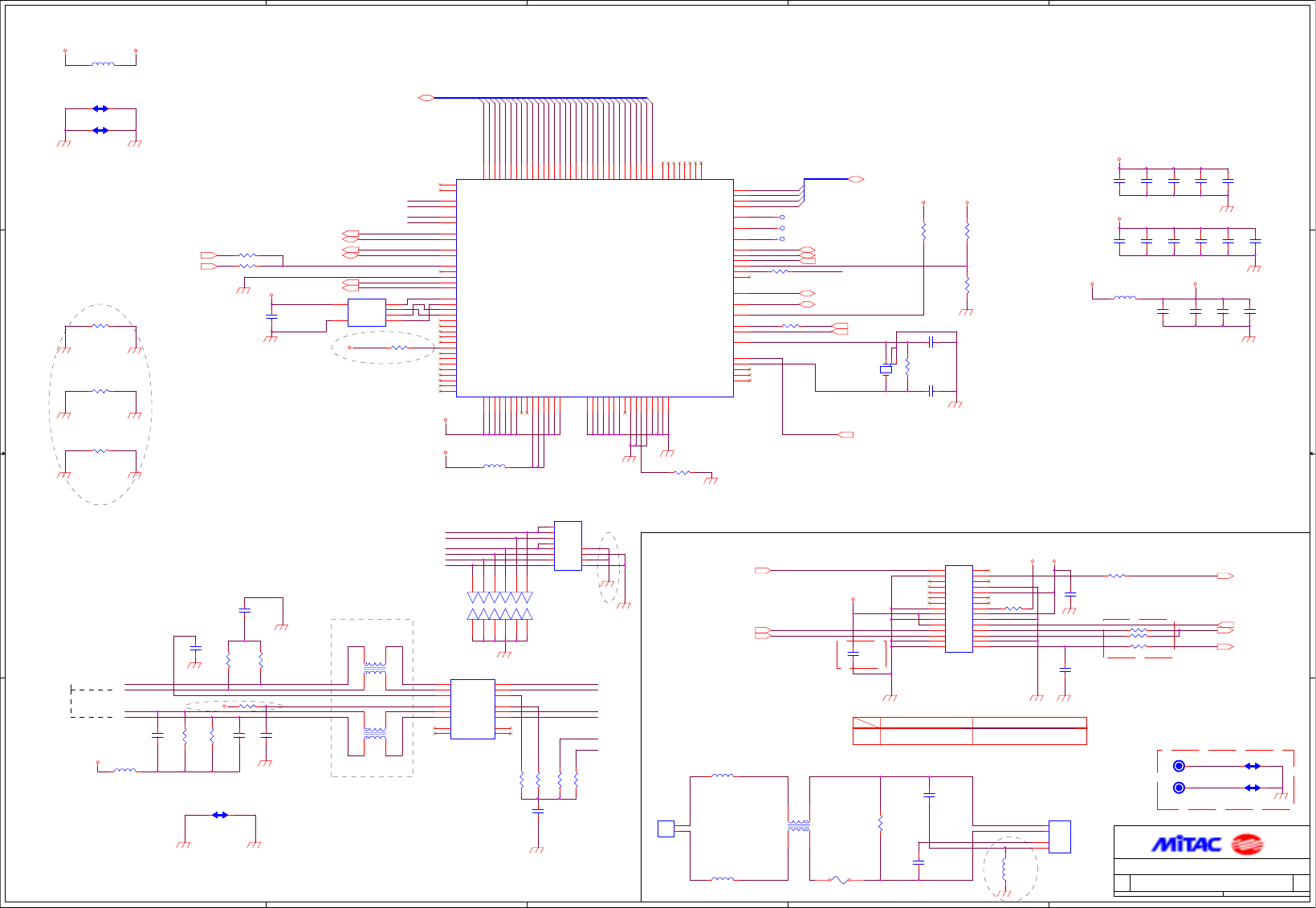
5
5
4
4
3
3
2
2
1
1
D D
C C
B B
A A
RJ11
PIN 16
HIGH LOW
MDC SCREW HOLE
AUDIO CODEC ON DAUGHTER BOARDAUDIO CODEC ON MOTHER BD
MDC HARDWARE STRAP
CLOSE TO MDC
Modem Dougther Board
Layout Note:
,
#%'()*+
EX: GND SHIELDING
S/W/W/S=12/6/6/12 mils
L_AGND
ǐ
#%##!" &$#
as short as possible
GND_45
L_AGND
GND_45
GND_45
RJ45
CLOSE TO MDC
FOR EMI
L_AGND
R01
R0,-->R02
R0,-->R02R0,-->R02
R0,-->R02
GND_16
FOR ESD ISSUE
R02
R02R02
R02
R02
R02R02
R02
411671200001 02
LANPHY,MDC
16 22Friday, December 28, 2001
Title
Size Document
Number
Rev
Date: Sheet of
-ACRST
MDC_GND1
MDC_GND2
MONO_OUT
AD4
AD[0..31]
AD8
AD26
RXIN+
-CBE0
-CBE2
AD28
AD16
AD0
AD18
AD24
-PCI_GNT1
LAN_WAKE
AD21
AD3
AD29
AD23
AD2
AD13
RXIN-
AD17
AD18
AD15
AD1
AD11
AD14
AD20
AD7
TXD+
AD27
AD10
-CBE1
AD9
AD12
-PCI_REQ1
AD25
AD5
AD30
TXD-
AD6
AD31
-CBE[0..3]
-CBE3
AD22
AD19
PJ4
ACSDOUT
PJTX-
PJ4
PJRX-
PJ7
PJ7
ACSYNC
RXIN-
RXIN+
TXD-
TXD+ PJTX-
PJRX-
PJTX+
PJRX+
MODEM_SPK
MSDIN
ACBITCLK
PJTX+
PJRX+
+5V
+3V
+3V
L_AGND
+3V_LAN
L_GND
+3V_LAN
+3VS
L_GND
L_AGND
AVDD_LAN
L_AGND
+3V_LAN
L_GND
+3V_LAN
+3V_LAN
L_AGND
+3V_LAN
AVDD_LAN
+3V
+3V
AVDD_LAN
AVDD_LAN
L_AGND
L_AGND
+3V
L513
PLP3216S
CHOKE_PLP3216S
1
4
2
3
R583 100 0603
1 2
S500
Protector
1808A
12
C657
0.1U
50V
0603
12
R64 4.7K
0603
1 2
J4
ST/MA-2
HIROSE
DF13-2P-1.25V
1
2
R696
0_DFS
0603
1 2
JO502
SHORT-SMT3
1 2
JO501
SHORT-SMT3
1 2
R697
0_DFS
0603
1 2
R63 22 0603
1 2
L1
50UH
CHOKE_WLT04020201
2
1
3
5
MTG24
ID2.8/OD5.0
1
L10 120Z/100M 1608
1 2
MTG25
ID2.8/OD5.0
1
J11
FM/0.8MM/H2.4
AMP C-179373
1
3
5
7
9
11
13
15
17
19
21
23
25
27
29
2
4
6
8
10
12
14
16
18
20
22
24
26
28
30
C120
0.1U
50V
0603
12
J13
1.016MM/H8.6
OCTEKCONN
PJS-OXSXT
1
2
GND1
GND2
1
2
GND1
GND2
R61 22 0603
1 2
C567
22P
0603
12
C572
22P
0603
12
C119
10P/NA
0603
12
R65 0_NA
0603
1 2
C597
0.1U
50V
0603
12
C88
0.1U
50V
0603
12
C57
0.1U
50V
0603
12
U4
RTL8139CL
PQFP128A_0.5MM
13
26
39
120
121
122
45
44
43
42
41
38
37
34
33
32
31
29
28
27
11
10
9
8
6
5
4
128
127
126
125
123
1
12
25
35
46
58
59
72
73
77
90
96
106
109
119
23
50
17
82
81
92
91
87
86
114
16
118
115
54
79
76
85
83
20
21
7
18
30
40
56
55
62
71
74
80
84
93
111
112
113
124
47
48
49
51
52
53
57
60
61
63
64
65
66
67
68
69
70
108
107
105
104
103
102
101
100
75
78
88
89
94
116
117
15
19
22
95
3
110
99
98
97
36
24
14
2
AD16
AD15
AD5
AD31
AD30
AD29
AD0
AD1
AD2
AD3
AD4
AD6
AD7
AD8
AD9
AD10
AD11
AD12
AD13
AD14
AD17
AD18
AD19
AD20
AD21
AD22
AD23
AD24
AD25
AD26
AD27
AD28
VDD0
VDD1
VDD2
VDD3
VDD4
VDD5
VDD6
NC5
NC6
VDD9
VDD10
VDD11
VDD12
VDD13
VDD14
PAR
EECS
TRDY#
RTT2
RTT3
TXD+
TXD-
RXIN+
RXIN-
INTA#
IRDY#
REQ#
RST#
NC0
XTALIN
PME#
GND
LWAKE
STOP#
PERR#
GND0
GND1
GND2
GND3
GND4
GND5
GND6
NC1
GND8
GND9
RTSET
GND11
GND12
GND13
GND14
GND15
MA0
MA1
MA2
MA3
MA4
MA5
MA6
MA7
MA8
MA9
MA10
MA11
MA12
MA13
MA14
MA15
MA16
MD0
MD1
MD2
MD3
MD4
MD5
MD6
MD7
CLKRUN#
XTALOUT
NC2
NC3
NC4
CLK
GNT#
FRAME#
DEVSEL#
SERR#
ISOLATE#
IDSEL
ROMCS#
LED0
LED1
LED2
CBE0#
CBE1#
CBE2#
CBE3#
C583
0.1U
50V
0603
12
U2
H0011
XFMR_H0009
16
15
14
11
10
9
12
135
4
8
7
6
3
2
1RX+
RX-
RXC
TXC
TX+
TX-
NC2
NC3NC1
NC0
TD-
TD+
TDC
RDC
RD-
RD+
F500
mircoSMDC110
1 2
C62
0.1U
50V
0603
12
R165 5.6K 0603
1 2
R15 0_DFS 0603
1 2
L508
PLP3216S
CHOKE_PLP3216S
1
4
2
3
R565
15K
0603
12
R571
1K
0603
12
C586
0.1U
50V
0603
12
R32 0_DFS 0603
1 2
C87
0.1U
50V
0603
12
C592
0.1U
50V
0603
12
R30 0/NA 0603
1 2
L21
120Z/100M
2012
1 2
L9 120Z/100M 1608
1 2
L22
120Z/100M
2012
1 2
C85
0.1U
50V
0603
12
C54
4.7U
16V
1206
12
R23
1.8K 0603 1%
1 2
R62 22 0603
1 2
R584
4.7K
0603
12
JO516
12
JO35
12
JS500
SHORT-SMT4
1 2
C86
0.1U
50V
0603
12
J9
8PX1/1.016MM
CONN_PJS-AST_8
1
2
3
4
5
6
7
8
GND1
GND2
GND3
GND4
1
2
3
4
5
6
7
8
GND1
GND2
GND3
GND4
R164
0_DFS
0603
1 2
R549
51
0603
12
R555
51
0603
12
C56
0.1U
50V
0603
12
JS4
SHORT-SMT4
1 2
U5
9346A
1
2
3
4
8
5
CS
SK
DI
DO
VCC
GND
C39
0.1U
50V
0603
12
C69
0.1U
50V
0603
12
C577
0.1U
50V
0603
12
C566
1000P
3KV
1808
10%
12
JS6
SHORT-SMT4
1 2
R541
51
0603
12
R542
51
0603
12
C40
0.1U
50V
0603
12
C584
10P
0603
1 2
C585
10P
0603
1 2
R566
1M_NA
0603
1 2
R17
75
0603
12
C65
2.2U
16V
1206
12
R531
75
0603
12
R12
75
0603
12
R530
75
0603
12
C84
0.1U
50V
0603
12
C81
2.2U
16V
1206
12
JO32
12
JO30
12
L511
120Z/100M
1608
1 2
JO31
12
JO512
12
L12 120Z/100M 1608
1 2
TP18
1
TP17
1
TP16
1
R31 0_DFS 0603
1 2
L25
120Z/100M
2012
1 2
X501
25MHZ
1 3
2
4
C500
1000P
3KV
1808
10%
1 2
C502
1000P
3KV
1808
10%
12
MODEM_SPK (17)
-ACRST(13,17)
MONO_OUT(17)
ACBITCLK (13,17)
MSDIN (13)ACSDOUT(13,17)
-PCIRST(7,10,13,18)
-PCI_INTD(13,14)
-PCI_REQ1(13,14) -DEVSEL (13,14,15)
-PME(13,15)
-PCLKRUN (14,15)
-IRDY(13,14,15)
-FRAME (13,14,15)
-CBE[0..3] (13,15)
PCICLK_LAN (8)
AD[0..31](13,15)
-PCI_GNT1 (13,14)
-TRDY(13,14,15)
-STOP (13,14,15)
PAR (13,15)
-SERR (13,14,15)
LAN_WAKE(19)
-PCIRST_N(13,15)
ACSYNC (13,17)
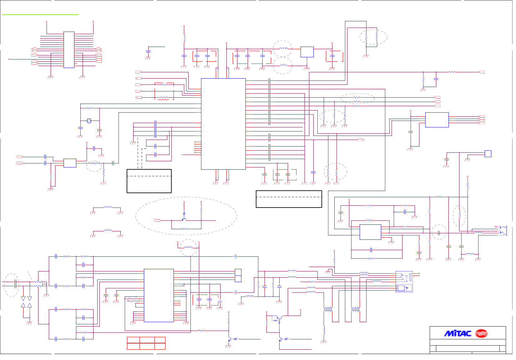
5
5
4
4
3
3
2
2
1
1
D D
C C
B B
A A
AGND
AGND
AGND
AGND
AGND
Cap pin33: 1U X
AGND
AGND
Very Close to Codec
ZV AUDIO
AGND
AGND
AGND
AGND
AGND
CHIP ALC201 CS4299
Cap. pin30: 1000P 270P 1000P
Cap pin32: 1U 0.01U
20mil
AGND
AGND
AGND
Cap. pin29: 1000P 270P 1000P
INTERNAL MICROPHONE
Close to 78L05
CLOSE TO CODEC
Cap pin31: 1U X
(NA J22,L525,
L530 For LCD 15")
AGND
Close to CodecClose to Codec
CHIP ALC2000 AD1881 CS4299
AGND
AGND
MIC
AGND
CAGND
AGND
AGND
AGND
AGND
AGND
AUDIO CODE & AMPLIFIER
External Micro Phone Jack
AGND
AGND
AGND
AGND
Cap p33/34 X 1000P
HI LOW
L
AGND
SPK_OFF
Very Close to TPA0202 Pin 18/7
R
(NA J20,J18 For LCD 15")
AGND
Signal
AGND
AGND
AGND CAGND
Internal Speaker Connector
(NA VR1,C717,C718
For LCD 15")
Normal
Amplifier
Shut Down
AGND
AOUT_R/L Cap x2 - SIZE0805
AGND
AGND
AGND
(NA L523,L524,L536,L532,
L527,L528,L531,L537,L538,
L539,J19 For LCD 15")
AGND
Line Out Phone Jack
AGND
(ADD J17 For LCD 15")
AGND
AGND
R01
R01
R01
R01
R01
R02
R02R02
R02
R02
R02
R02R02
R02
R02
R02R02
R02
R02
R02R02
R02
R02
R02R02
R02
R02
R02R02
R02
R02
R02R02
R02
02
AUDIO CODEC & AMPLIFIER
17 22Friday, December 28, 2001
411671200001
Title
Size Document
Number
Rev
Date: Sheet of
MIC
CDROM_LEFT
-ACRST
CDROM_COMM
MIC1
MIC2
VIDEO_L
MONO_OUT
-CARDSPK
AOUT_L
AOUT_R
ACSDIN
CDROM_RIGHT
ACSYNC
MODEM_SPK
ACBITCLK
ZV_SCLK
ZV_DATA
SPDIFOUT
ZV_LRCLK
VIDEO_R
ZV_MCLK
ACSDOUT
SPK_OFF
MUTE_IN
VR1_5
VR1_2
SPKROUT-
SPKLOUT-
-DECT_HP/OPT
SPDIFOUT
-DEVICE_DECT
SBSPKR
-HDDACTP -CDACTP
SPKLOUT-
-DEVICE_DECT
AOUT_L
T_DATA
TPB1-
-DECT_HP/OPT
SPKLOUT+
LINE_OUT_2
TPA1-
MIC_2
SPKROUT+
T_CLK
SPDIFOUT
SPKLOUT+
-DEVICE_DECT
AOUT_R
-CAP
TPA1+
-NUM
-DEVICE_DECT
MIC_3
LINE_OUT_5
TPB1+
SPKROUT+
VR1_5VR1_2
ACBITCLK
SPKROUT-
-SCROLL
LINE_OUT_2
LINE_OUT_5
AOUT_L
AOUT_R
MIC_3
-DECT_HP/OPT
MIC_2
MUTE_IN
AVDDAD
+3VS
+5VS
AVDDAD
+12VS
AVDDAD
5V_AMP
5V_AMP +3VS
5V_AMP
5V_AMP
+5VS
+5VS
AVDDAD
+3VS_SPD
+3VS_SPD
+5V
+3V_ICH +5VS
U513
MC33078D
3
21
5
67
8
4
1IN+
1IN-1OUT
2IN+
2IN-2OUT
VCC+
VCC-
R666
10K
0603
1%
1 2
C704 220P 060310%
1 2
L527
120Z/100M
1608
1 2
+
C166
100U
16V
EW6.3
12
R102
47K
0603
12
R1
Q10
DTC144TKA
2
1
3
R1
Q16 DTC144TKA
2
1 3
R664
10K
0603
1%
1 2
U15
ALC201
PQFP48_0.5MM
19
2
3
12
24
23
20
18
17
16
15
14
13
37
39
41
34
1
9
25
38
4
7
26
42
21
22
35
36
31
32
33
11
5
8
10
6
27
28
29
30
40
43
44
45
46
47
48
CD/GND
XTL/IN
XTL/OUT
PC_BEEP
LINE/IN/R
LINE/IN/L
CD/R
CD/L
VIDEO/R
VIDEO/L
AUX/R
AUX/L
PHONE
MONO_OUT
ALT_LINE_OUT_L
ALT_LINE_OUT_R
FLTO
DVDD1
DVDD2
AVDD1
AVDD2
DVSS1
DVSS2
AVSS1
AVSS2
MIC1
MIC2
LINE/OUT/L
LINE/OUT/R
BPCFG
FLT3D
FLTI
RESET#
SDATA/OUT
SDATA/IN
SYNC
BIT/CLK
REFFLT
VREFOUT
AFLT1
AFLT2
NC1
NC2
NC3
ID0#
ID1#
EAPD
S/PDIF_OUT
C185 1U 060310V
1 2
C142 1U 060310V
1 2
R151
6.8K
0603
5%
12
C68610U 10V 1206
1 2
L17
120Z/100M
2012
1 2
X2
24.576MHZ
1 2
U510
NC7S32
SC70/SOT70
1
2
3
5
4
A
B
GND
VCC
Y
C676
47P_NA
0603
12
R149
100K
0603
12
R113
100K
0603
1 2
U18
TPA0202_GND TSSOP24_TPA0102
22
15
3
10
18
7
1
12
13
24
2
17
23
21
20
19
4
5
6
14
16
11
9
8
25
26
27
28
29
30
31
32
33
34
R OUT+
R OUT-
L OUT+
L OUT-
RVDD
LVDD
GND0
GND1
GND2
GND3
NC0
NC1
NC2
RLINE IN
RHP IN
R BYPASS
LLINE IN
LHP IN
L BYPASS
SE/BTL#
HP/LINE#
MUTE IN
MUTE OUT
SHUTDOWN
G1
G2
G3
G4
G5
G6
G7
G8
G9
G10
R148
68K
0603
12
R647
20K
0603
12
L26
120Z/100M
2012
1 2
R671 4.7K 0603
1 2
R646
200K
0603
1 2
C701
0.068U
25V 0805
1 2
C133
1000P/NA
0603
12
R657
0_DFS
0603
1 2
R668 2.7K 0603
1 2
R659
10K
0603
12
C700
0.1U
50V
0603
12
C159
0.1U_NA 50V 0603
1 2
R673
4.7K 0603
1 2
R109
6.8K_DFS
5%
12
L18
120Z/100M
2012
1 2
R669 47K 0603
1 2
R685
10K
0603
12
C141 1000P 060350V
1 2
L525 120Z/100M 1608
1 2
R121
6.8K_DFS
5%
12
C165
0.1U_NA 50V 0603
1 2
R667
15K
0603
1%
1 2 L530 120Z/100M
1608
1 2
R670 47K 0603
1 2
C179
1U
0603
10V
12
C180
0.1U
50V
0603
12
C172
0.1U
50V
0603
12
U512
CS4334/NA
SO8
1
2
3
4
7
8
5
6
SDATAI
SCLK
LRCK
MCLK
VA+
AOUTL
AOUTR
AGND
C697
0.1U/NA
50V
0603
12
C665
0.1U
50V
0603
12
VR1
10K
1
2
3
4
5
6
7
R649
47K
0603
12
JO33
12
L536
PLP3216S
CHOKE_PLP3216S
1
4
2
3
JO34
12
R653
0_DFS
0603
1 2
C206
0.1U
50V
0603
12
C168
0.1U
50V
0603
12
J16
ST/MA-2
HIROSE
DF13-2P-1.25V
1
2
L535
120Z/100M_DFS
1608
12
L.CH
R.CH
J22
RA/D3.6/5P
HCH
IDJ-B27-F6T
1
2
3
4
5
C666
10P
0603
12
C209
10U
10V
1206
12
C705
220P/NA
0603
10%
12
C667
0.1U
50V
0603
1 2
U511
L78L05ACU
SOT89N 31
2
IO
GND
C669
0.1U
50V
0603
1 2
C207
1U
0603
12
C169
1U
0603
12
C696
220P/NA
0603
10%
12
R652
10K 0603
1 2
C674
0.1U
50V
0603
12
LED
Drive
IC
J19
2F1138-TJ1
FOXCONN
5
4
2
3
1
7
8
9
6
11
R167 0/NA 0603
1 2
L532
PLP3216S
CHOKE_PLP3216S
1
4
2
3
L522
BEAD
0805C
1 2
R679 22K 0603
1 2
C183 2.2U 0805 +80-20%
1 2
C196 2.2U 0805 +80-20%
1 2
R141
0
0603
1 2
R133 0 0603
1 2
L540
120Z/100M
2012
1 2
L538 120Z/100M 1608
1 2
L537 120Z/100M 1608
1 2
C146
10U_NA
10V
1206
12
R143
1K
0603
12
R166
10K
0603
12
L539 120Z/100M 1608
1 2
C702
0.1U
50V
0603
12
C672
0.1U
50V
0603
12
C668
0.1U
50V
0603
12
C689
100P
0603
12
L529
120Z/100M
1608
12
R645 22 0603
1 2
C692
470P
0603
10%
1 2
R648 22 0603
1 2
L14
120Z/100M
1608
12
R122
1K
0603
12
J18
ST/MA-2
HIROSE
DF13-2P-1.25V
1
2
C691
470P
0603
10%
1 2
C717 4.7U 0805 +80-20%
1 2
C684
10U
10V
1206
12
J20
ST/MA-2
HIROSE
DF13-2P-1.25V
1
2
C191 1U 060310V
1 2
C193 1U 060310V
1 2
C718 4.7U 0805 +80-20%
1 2
+
C204 220U 10V EW6.3
1 2
+
C210 220U 10V EW6.3
1 2
C158
1000P_NA
0603 50V 1 2
C694
470P
0603
10%
1 2
R88
1M0603
1 2
C675 0.1U 50V 0603
1 2
C1601U0603 10V 1 2
L523 120Z/100M 1608
1 2
C167
10P
0603
12
L524 120Z/100M 1608
1 2
C688
100P
0603
12
C148
10P
0603
12
L528 120Z/100M 1608
1 2
J17
HDR/MA/1.27MM/NA
S100-0112-321
SPEED
1
3
5
7
9
11
13
15
17
19
21
2
4
6
8
10
12
14
16
18
20
22
2423
25 26
27 28
29 30
31 32
1
3
5
7
9
11
13
15
17
19
21
2
4
6
8
10
12
14
16
18
20
22
2423
25 26
27 28
29 30
31 32
C693
470P
0603
10%
1 2
L531 120Z/100M 1608
1 2
C132 1000P 060350V
1 2
C670
0.1U
50V
0603
1 2
C173 1000P 060350V
1 2
Q514
DTA144WK
1
2
3
R1
Q515
DTC144TKA 2
1
3
C174 1000P 060350V
1 2
C687
0.1U_NA
50V
0603
12
C188 1U 060310V
1 2
C194 1U 060310V
1 2
C1631U0603 10V 1 2
C710
2.2U
0805
+80-20%
1 2
C709
2.2U
0805
+80-20%
1 2
R663
40.2K/NA
0603
1%
12
R655
1K
0603
12
C707
2.2U
0805
+80-20%
1 2
R665
15K
0603
1%
1 2
C708
2.2U
0805
+80-20%
1 2
C192 1U 060310V
1 2
C186 1U 060310V
1 2
C190 1U 060310V
1 2
R678
10K
0603
1%
1 2
C189 1U 060310V
1 2
C1641U0603 10V 1 2
R677
10K
0603
1%
1 2
R140
100K
0603
12
R142
100K
0603
12
R676
10K
0603
1%
1 2
R134 1K 0603
1 2
R675
10K
0603
1%
1 2
R132 1K 0603
1 2
R6800/NA 0603
1 2
C202 1U 060310V
1 2
MODEM_SPK (16)
ACSDOUT(13,16)
-CARDSPK(15)
CDROM_COMM (14)
ACBITCLK(13,16)
CDROM_LEFT (14)
ACSYNC(13,16)
ACSDIN(13)
ZV_MCLK (15)
ZV_SCLK (15)
ZV_LRCLK (15)
ZV_DATA (15)
MONO_OUT (16)
-ACRST(13,16)
CDROM_RIGHT (14)
SBSPKR(13)
SPK_OFF(13)
-CAP(12,19)
TPA1- (15)
TPA1+ (15)
TPB1-(15) TPB1+(15)
T_CLK (18,19)
-CDACTP (14,19)
-HDDACTP(14,19)
-SCROLL (12,19)
-NUM (12,19)
T_DATA(18,19)
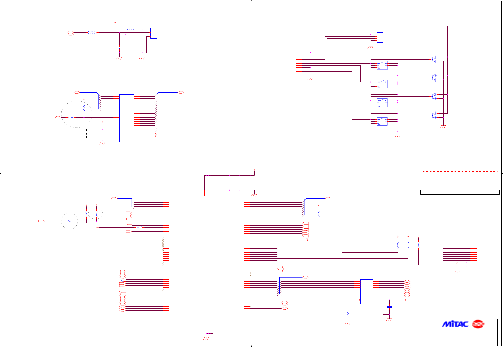
A
A
B
B
2 2
1 1
Flash ROM
Close to EEPROM
TOUCH_PAD
Flash ROM
SCRL UP
SCRL DOWN
RIGHT
LEFT
XCNF0
XCNF1
FUNCTIONALITY
1
1
LATCH MODE , XA12-19, XRDY DISABLE
BASE ADDRESS SELECT
X
XCNF0
10
4EH
1
NO BIOS
0
1
LATCH MODE , GPIO 10-17 ,XRDY DISABLE
XCNF1
0
1
LATCH MODE , GPIO 10-17 , XRDY ENABLE
OPEN
0
2FH
STRAP OPTION
XCNF2
0
INDEX REGISTER
1
0
1
NORMAL MODE , XRDY DISABLE
MOUNTED
1
4FH
X
R303
2EH
DATA REGISTER
0
LATCH MODE ,XA12-19, XRDY ENABLE
(NA L13,L15,L16,C139,
C149,C135,J15 For LCD 15")
R01
R01
R0,-->R02
R0,-->R02R0,-->R02
R0,-->R02
2M ROM------PULL VCC
4M ROM------SA18
411671200001 02
TOUCH PAD,BIOS,SUPER-IO
Custom
18 22Friday, December 28, 2001
MITAC INTERNATIONAL CORP.
Title
Size Document Number Rev
Date: Sheet of
SA14
SD0[0..7]
-ROMCS
-IOR
SA12
COM1RXD
SA13
SA0
SA3
FIRSEL
-LFRAME
-COM1RTS
IRQ12
-MCCS
-COM1DTR
PCICLK_LPC
-IOW
PIO/-PNF
-COM1DCD
-COM1CTS
-PCIRST
SA17
SA16
SA2
COM1TXD
-LDRQ
SA1
-MEMR
SERIRQ
SA18
IRRX
SIO_14.318MHZ
-XSTB
IRTX
-MEMW
-COM1RI
SA15
-COM1DSR
SA5
SA9
SA7
SA8
SA4
-XSTB
SA10
SA6
SA11
SA19
-SUS_STAT
SD1
SD0
LAD3
SD6
LAD0
SD7
SD4 SD3
LAD2
P_LPD[0..7]
SD5
SD0
P_LPD1
SD4
SD2 SD1SD1
SD3
LAD1
SD6
P_LPD3
SD2SD2SD2
P_LPD2
LAD[0..3]
SD5
SD7
-CLKRUN
-COM1RI
COM1TXD
-COM1DSR
-COM1RTS
-COM1DCD
COM1RXD
-COM1DTR
-COM1CTS
SA1
SD3
SA[0..17]
SD0
SA13
SD2
SA0
SD5
-ROMCS
SA17
T_DATA
SD6
SA10
T_CLK
SA6
SA16
SD[0..7]
SA2
-MEMW
SA5
SA14
SD7
SA12
SD1
SA8
-MEMR
SA3
SA9
SA11
SA4
SD4
SA15
SA7
SCRL_DOWN
TP_VCC
CLK
RIGHT
DATA
SCRL_UP
LEFT
-LPCPD
-MEMW
COM1TXD
IRQ1
XCNF2
-P_INIT
-P_STB
-P_AFD
-P_ACK
-P_SLIN
-P_ERR
P_PE
P_BUSY
P_SLCT
P_LPD6
P_LPD4
P_LPD0
P_LPD7
P_LPD5
+3VS
+3VS
+3VS+3VS
+3VS +3VS+3VS
+3VS
+5V
+5VS
TP_GND
TP_GND
TP_GND
TP_GND
+3VS
+3VS
+5VS
R638
0_DFS
0603
1 2
U12
28F020-PLCC
12
11
10
9
8
7
6
5
27
26
23
25
4
28
29
3
2
22
24
1
31
13
14
15
17
18
19
20
21
32
16
30
A0
A1
A2
A3
A4
A5
A6
A7
A8
A9
A10
A11
A12
A13
A14
A15
A16
CE#
OE#
VPP
WE#
O0
O1
O2
O3
O4
O5
O6
O7
VCC
VSS
A17
U11
74AHC373_V
TSSOP20
282574373004
3
4
7
8
13
14
17
18
1
11
2
5
6
9
12
15
16
19
20
10
D0
D1
D2
D3
D4
D5
D6
D7
OC
G
Q0
Q1
Q2
Q3
Q4
Q5
Q6
Q7
VCC
GND
L13 120Z/100M 1608
1 2
C653
0.1U
50V
0603DA
12
C123
0.1U
50V
0603
12
C660
0.1U
50V
0603DA
12
R640
10K
0603
12
C139
47P
0603
12
C105
0.1U
50V
0603DA
12
SW4
12V/50MA
STS-042-A
1
23
4
5
C149
47P
0603
12
R639
10K/NA
0603
12
C664
0.1U
50V
0603DA
12
R644
10K
0603
12
U509
PC87393
PQFP100_0.5MM
284587393002
15
16
17
18
8
9
12
11
7
6
10
19
20
21
22
23
24
25
26
27
28
29
30
31
32
33
34
95
94
93
92
91
90
87
86
85
84
83
82
81
80
79
78
77
76
75
74
52
50
48
46
45
44
43
42
35
36
37
40
41
47
49
51
53
54
55
56
57
58
59
60
61
62
70
69
68
67
66
3
2
1
100
99
98
97
96
4
5
73
71
72
13
38
64
89
14
39
63
88
LAD0
LAD1
LAD2
LAD3
LCLK
LRESET#
LFRAME#
LDRQ#
LPCPD#
CLKRUN#/GPIO36
SERIRQ
SMI#/GPIO35
CLKIN
DSKCHG#
HDSEL#
RDATA#
WP#
TRK0#
WGATE#
WDATA#
SETP#
DIR#
DR0#
MTR0#
INDEX#
DENSEL
DRATE0/IRSL2
XA0/GPIO20
XA1/GPIO21
XA2/GPIO22
XA3/GPIO23
XA4/GPIO24/XSTB0#
XA5/XSTB1#/XCNF2
XA6/GPIO26/PRIQA/XSTB2#
XA7/GPIO27/PIRQB
XA8/GPIO30/PIRQC
XA9/GPIO31/MTR1#/PIRQD
XA10/GPIO32/XIORD#/MDRX
XA11/GPIO33/XIOWR#/MDTX
XA12/GPIO10/JOYABTN1/RI2#
XA13/GPIO11/JOYBBTN1/DTR2#_BOUT2
XA14/GPIO12/JOYAY/CTS2#
XA15/GPIO13/JOYBY/SOUT2
XA16/GPIO14/JOYBX/RTS2#
XA17/GPIO15/JOYAX/SIN2
XA18/GPIO16/JOYBBTN0/DSR2#
XA19/DCD2#/JOYABTN0/GPIO17
PD0/INDEX#
PD1/TRK0#
PD2/WP#
PD3/RDATA#
PD4/DSKCHG#
PD5/MSEN0
PD6/DRATE0
PD7/MSEN1
PNF/XRDY
SLCT/WGATE#
PE/WDATA#
BUSY_WAIT#/MTR1#
ACK#/DR1#
SLIN#_ASTRB#/STEP#
INIT#/DIR#
ERR#/HDSEL#
AFD#_DSTRB#/DENSEL
STB#_WRITE#
DCD1#
DSR1#
SIN1
RTS1#/TEST
SOUT1/XCNF0
CTS1#
DTR1#_BOUT1/BADDR
RI1#
IRTX
IRRX1
IRRX2_IRSL0
IRSL1
IRSL3/PWUREQ#
XD0/GPIO00/JOYABTN1
XD1/GPIO01/JOYBBTN1
XD2/GPIO02/JOYAY
XD3/GPIO03/JOYBY
XD4/GPIO04/JOYBX
XD5/GPIO05/JOYAX
XD6/GPIO06/JOYBBTN0
XD7/GPIO07/JOYABTN0
XWR#/XCNF1
XRD#/GPIO34/WDO#
XIOWR#/XCS1#/MTR1#/DRATE0
XIORD#/GPIO37/IRSL2/DR1#
XCS0#/DR1#/XDRY/GPIO25
VSS0
VSS1
VSS2
VSS3
VDD0
VDD1
VDD2
VDD3
R637
10K
0603
12
C656
0.1U
50V
0603DA
12
D4
BAV99
1
2
3
TP545 1
D3
BAV99
1
2
3
L16 120Z/100M 1608
1 2
J500
HDR/MA-8
ACES
88206-0800
GND2
GND1
1
2
3
4
5
6
7
8
J501
ST/MA-4
HIROSE
DF13-4P-1.25V
1
2
3
4
R635
10K
0603
12
R58
10K
0603
12
C135
0.1U
50V
0603
12
SW3
12V/50MA
STS-042-A
1
23
4
5
SW2
12V/50MA
STS-042-A
1
23
4
5
D6
BAV99
1
2
3
D1
BAV99
1
2
3
L15 120Z/100M 1608
1 2
R643
10K/NA
0603
12
J15
ST/MA-4
HIROSE
DF13-4P-1.25V
1
2
3
4
SW1
12V/50MA
STS-042-A
1
23
4
5
J506
FFC-12P/0.5MM/NA
1
2
3
4
5
6
7
8
9
10
11
12
1
2
3
4
5
6
7
8
9
10
11
12
R163
0_DFS 0603
1 2
R162
0/NA
0603
12
R64110K/NA 0603
1 2
LAD[0..3](13)
IRQ12(14,19)
-MEMR (14)
-MCCS (14,19)
SD[0..7] (14,19)
SA12(14) SA13(14) SA14(14) SA15(14) SA16(14) SA17(14) SA18(14) SA19(14)
SA4 (14)
SA5 (14)
SA7 (14)
SA8 (14)
SA9 (14)
SA10 (14)
SA11 (14)
SA6 (14)
-ROMCS (19)
P_LPD[0..7] (22)
P_SLCT (22)
P_BUSY (22)
-P_ACK (22)
-P_SLIN (22)
-P_INIT (22)
-P_ERR (22)
-P_AFD (22)
-P_STB (22)
IRRX (22)
IRTX (22)
FIRSEL (22)
-SUS_STAT(10,13)
SA0(14) SA1(14) SA2(14,19) SA3(14)
P_PE (22)
SA[0..17] (14,19)
SA18(14)
SD[0..7](14,19)
-ROMCS (19)
-MEMR (14)
T_DATA(17,19) T_CLK(17,19)
-PCIRST(7,10,13,16)
PCICLK_LPC(8)
-LFRAME(13) -LDRQ(13)
SERIRQ(13,14,15)
SIO_14.318MHZ(8)
-IOR(14,19) -IOW(14,19)
IRQ1(14,19)
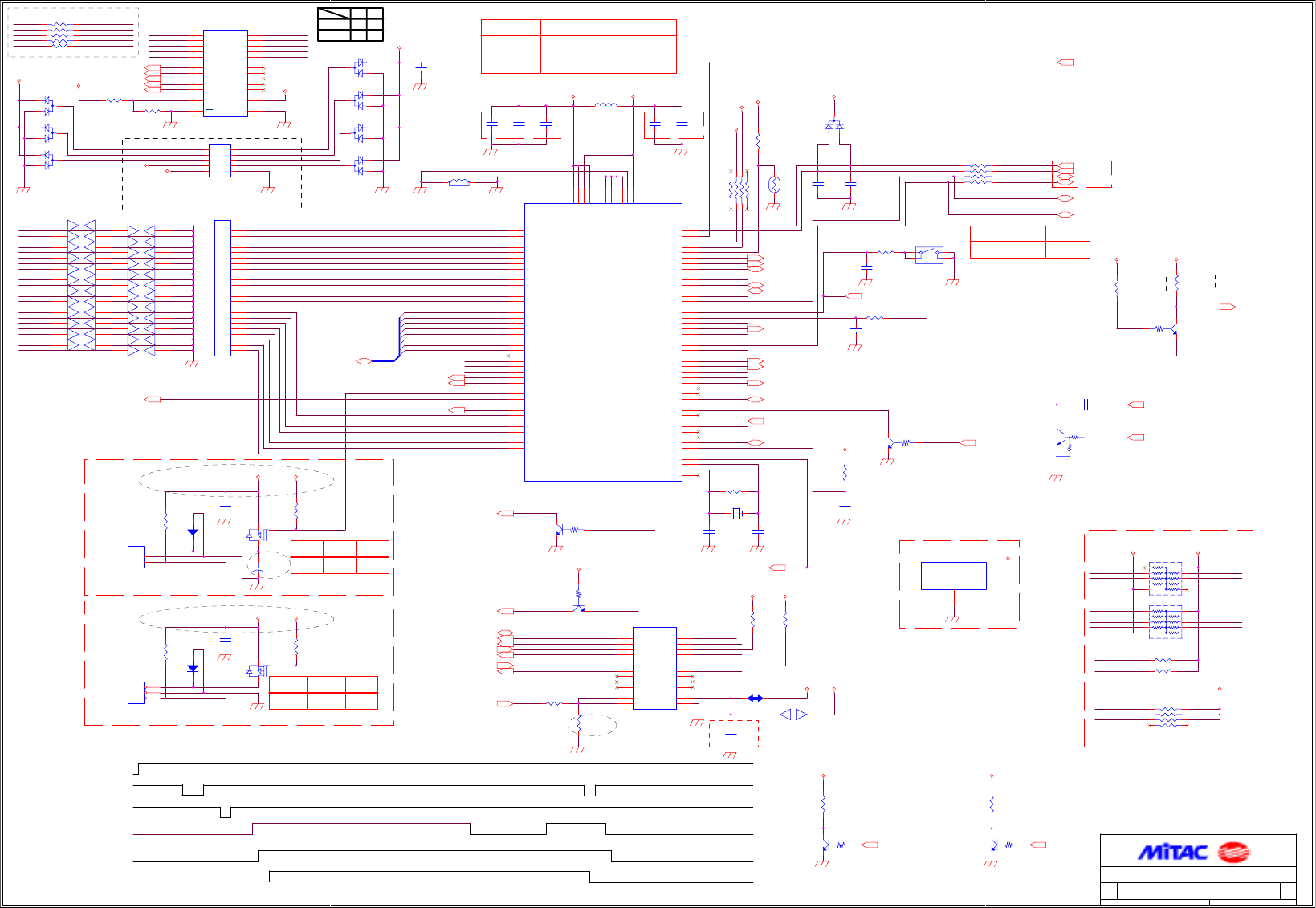
A
A
B
B
2 2
1 1
Normal
FAN
HI
-LID
-FAN
Come From Battery
Close to SI2301DS
Controller
Close to H8-3437F
For H8-3437F Reset
Signal
GND_H8
HI
Signal LOW
FAN On
External Pull Up/Down
GND_H8
Threshold : 4.38V
FAN Off
Micro
Suspend
CPU_FAN Control
GND_H8
LOW
Internal Keyboard
Connector
Close to H8-3437F
VDD3 ON then through R/C to generate -RSMRST.
PWROK(H8 O/P)
ICH2 received -H8_ICH2BTN(H8 O/P), then o/p -SUSB-C.
-POWERBTN(H8 I/P)
-H8_ICH2BTN(H8 O/P)
ALL POWER
-SUS[B-C](SB O/P)
H8(Pin 40) detect powebtn,then delay 100ms to o/p -MVP4BT pulse(1us) to SB..
-RSMRST(SB I/P)
H8's pin14 PWR_ON on VCC3/5 then Vcore/Vtt/Vcc25.
H8 detect -SUSC,then delay 150ms then o/p PWROK.
Power switch ON.
Into S4 Resume
Power switch OFF
H8 OFF this pin before o/p PWRON low..
Cover Switch
AGND
(NA C638,R629,SW6 For LCD 15")
Level Shift
Close to 74CBTD3384DBQ
LOW
FAN Off
FAN
-DC/DC_FAN Control
HISignal
Close to SI2301DS
-DC/DC_FAN FAN On
ICN2 INTERNAL PULL UP
MODE3
H8 Mode Select Table
Description
1
1
MD1
Expended mode with On-Chip ROM disableMODE1
1
MD0 MODE
Expended mode with On-Chip ROM enable1
Single-Chip mode
MODE2
0
0
EASY START BTN/LED INDICATOR
LED
QK-B
BX BE#
LL
HL
NA RP521,R693,R691 FOR 8175 QK-B
R01
R01
R01
NA RP521,R693,R692 FOR 8175 LED-B
R02
R02R02
R02
411671200001 02
Micro Controller
19 22Friday, December 28, 2001
Custom
Title
Size Document
Number
Rev
Date: Sheet of
-PWRSW
CHARGING
H8_MODE0
-H8_SMI
KI4
-POWERBTN
IRQ12
LED_CLK
KI0
BAT_V
KI7
-BATT_DEAD
BAT_DATA
KI1
-H8_STBY
-IOW
KI0
H8_MODE0
-RI
H8_MODE1
-H8_MCCS
SW_+5V A
T_CLK
KI3
KI6
BAT_VOLT
KI2 KI5
KI6
-H8_RESET
BAT_CLK
H8_A20GATE
BAT_D
BATT_DEAD
-IOR
-BATT_DEAD
-H8_SUSC
SA2
BLADJ
-H8_RCIN
-POWERBTNH8_MODE1
-ADEN
H8_PWROK
H8_SCI
-H8_WAKE_UP
BAT_CLK
BAT_C
LED_DATA
BAT_TEMP
-H8_KBCS
IRQ1
BAT_T
SD[0..7]
KI7
LEARNING
H8_A20GATE
T_DATA
-H8_ICH2BTN
-H8_THRM
-LID
-LID
T_CLK
PWR_ON H8_PWRON
-FAN1
BAT_DATA
-PWRBTN
-H8_ICH2BTN
-H8_SUSB
-H8_SUSC-H8_SUSB
SD1
SD2
SD7
SD0
SD5
SD3
SD6
SD4
LAN_WAKE
-RI
-FAN0
KO14
KI4
KO8
KO2
KO10
KI5
KI1
KO3
KO7
KO9
KO0
KO6
KO12
KO1
KO15
KO4
KO13
KO5
KO11
KO0
KO2
KO4
KO6
KO8
KO10
KO12
KO14
KI0
KI2
KI4
KI6
KO1
KO3
KO5
KO7
KO9
KO11
KO13
KO15
KI1
KI3
KI5
KI7
-H8_WAKE_UP
-H8_THRM
-EXTSMI
-ROMCS H8_A20GATE
-H8_RCIN
PWROK
-THRM
H8_PWROK
-WAKE_UP
-RCIN
ICH_A20GATE -H8_KBCS
-H8_MCCS
-H8_SMI
-FAN0
H8_SCI
-SCI
FAN0_SPD
FAN1_SPD
FAN1_SPD
-ADEN
-MCCS
T_DATA
-NUM_KI2
KI2
KI3
-SCROLL_KI1
-CDACTP_KI4
-HDDACTP_KO1
KI1
KI2
KI4
-PWRSW
-CAP
-CDACTP
-HDDACTP
-SCROLL
-NUM
KO0
-HDDACTP_KO1
-SCROLL_KI1
-CAP_KI3
-CAP_KI3
-NUM_KI2
KI3 -CDACTP_KI4
KO1
-SCROLL_KI1
-CAP_KI3
-CDACTP_KI4
-NUM_KI2
-HDDACTP_KO1
KI3
KI1
KI2
KI4
KO1
FAN0_SPD
+5VA
+5VA +5VA
+5V
+5VA
H8_VDD5
+5VS
+5VA +5VA
+5VA
+5VA+5VA
+1.8VS
+5VS
+3V_ICH+5V
+5VS +5VA
+5VA+5VA
+5VS
+5V
+3V_ICH
+5VA
+5V
+5VS
+5VS_LEDB
+5VS_LEDB
+5V
+5V
R692100K/NA
0603
1 2
JO7
12
J502
DF13-3P-1.25H
1
2
3
1
2
3RP511
4.7K*4
1206
1
2
3
4
8
7
6
5
D
SG
Q509
AO3401
G
D S
JO6
12
JO9
12
JO8
12
Q512
DTC144WK
1
2
3
R636
10K
0603
12
JO11
12
D7
RLS4148
AK
JO10
12
JO13
12
R660
10K
0603
12
JO12
12
JO15
12
R688
10K
0603
12
R687
10K
0603
12
U515
SN74CBTH3383/NA
SSOP24
7
8
11
14
17
18
21
22
1
13
2
5
6
9
10
15
16
19
20
23
24
12
3
4
2A1
2A2
3A1
3A2
4A1
4A2
5A1
5A2
BE
BX
1B1
1B2
2B1
2B2
3B1
3B2
4B1
4B2
5B1
5B2
VCC
GND
1A1
1A2
D
SG
Q1
AO3401
G
D S
R1
470K
0603
12
JO14
12
JO17
12
C4
0.1U
50V
0603
12
JO4
12
+
C720
220U/NA
7343
10V
12
JO16
12
JO19
12
JS9
SHORT-SMT3
1 2
RP515
47K*8 1206
1
2
3
4
5 6
7
8
9
10
D506
BAV99
1
2
3
R642
470K
0603
12
RP512
47K*8 1206
1
2
3
4
5 6
7
8
9
10
U13
SN74CBTD3384
QSOP24A
3
4
7
8
11
14
17
18
21
22
15
16
19
20
23
2
5
6
9
10
1
13 24
12
1A1
1A2
1A3
1A4
1A5
2A1
2A2
2A3
2A4
2A5
2B1
2B2
2B3
2B4
2B5
1B1
1B2
1B3
1B4
1B5
1OE#
2OE# VCC
GND
L520
120Z/100M
1608
1 2
JO28
OPEN-SMT3
1 2
R629
1K
0603
1 2
R1
Q510
DTC144TKA
2
1
3
U508
H8/F3437S PQFP100_0.5MM
79
78
77
76
75
74
73
72
67
66
65
64
63
62
61
60
82
83
84
85
86
87
88
89
49
50
51
52
53
54
55
56
14
13
12
26
27
28
29
32
33
34
35
38
39
40
41
42
43
44
45
93
94
95
96
97
98
99
25
24
23
22
19
18
17
16
6
5
48
47
91
90
81
80
69
68
58
57
31
30
21
20
11
10
8
7
1
2
3
4
9
15
37
36
46
59
70
71
92
100
P10/A0
P11/A1
P12/A2
P13/A3
P14/A4
P15/A5
P16/A6
P17/A7
P20/A8
P21/A9
P22/A10
P23/A11
P24/A12
P25/A13
P26/A14
P27/A15
P30/HDB0/D0
P31/HDB1/D1
P32/HDB2/D2
P33/HDB3/D3
P34/HDB4/D4
P35/HDB5/D5
P36/HDB6/D6
P37/HDB7/D7
P40/TMCI0
P41/TMO0
P42/TMRI0
P43/TMCI1/HIRQ1
P44/TMO1/HIRQ1
P45/TMRI1/HIRQ1
P46/PW0
P47/PW1
P50/TXD0
P51/RXD0
P52/SCK0
P60/KEYIN0/FTCI
P61/KEYIN1/FTOA
P62/KEYIN2/FTIA
P63/KEYIN3/FTIB
P64/KEYIN4/FTIC
P65/KEYIN5/FTID
P66/KEYIN6/IRQ6
P67/KEYIN7/IRQ7
P70/AN0
P71/AN1
P72/AN2
P73/AN3
P74/AN4
P75/AN5
P76/AN6/DA0
P77/AN7/DA1
P80/HA0
P81/GA20
P82/CS1
P83/IOR
P84/IRQ2/TXD1/I
P85/IRQ4/RXD1/C
P86/IRQ5/SCK1/S
P90/IRQ2/ESC2
P91/IRQ1/EIOW
P92/IRQ0
P93/RD
P94/WR
P95/AS
P96/0
P97/WAIT/SDA
MD0
MD1
PA0/KEYIN8
PA1/KEYIN9
PB0/XDB0
PB1/XDB1
PB2/XDB2
PB3/XDB3
PB4/XDB4
PB5/XDB5
PB6/XDB6
PB7/XDB7
PA2/KEYIN10
PA3/KEYIN11
PA4/KEYIN12
PA5/KEYIN13
PA6/KEYIN14
PA7/KEYIN15
/STBY/FVPP
/NMI
/RES
XTAL
EXTAL
VCCB
VCC1
VSS4
AVCC
AVREF
AVSS
VCC2
VSS1
VSS2
VSS3
/RESO
X503
16MHZ
TXC8X4.5
1 2
JO18
12
C655
0.1U
50V
0603
12
R66
10K
0603
12
R1
Q511
DTC144TKA
2
1
3
JO21
12
C661
0.1U
50V
0603
12
J7
ST/MA-3
HIROSE
DF13-3P-1.25V
1
2
3
C659
0.1U
50V
0603
12
D510
BAV70LT1
1
23
J5
HDR/SHR/MA/5PX2
SPEED
S100-0000-101
21 43 6
8
5
10
7
9
R631 10K
0603
1 2
R693 0 0603
1 2
R4
10K
1%
12
RP518 33*4
1206
1
2
3
4
8
7
6
5
C632
0.1U
50V
0603
12
R67
0_DFS
0603
12
R1
Q506
DTC144TKA 2
1
3
C638
2.2U
16V
1206
1 2
C658
0.1U
50V
0603
12
R1
Q513
DTC144TKA
21
3
RP510
1K*4
1206
1
2
3
4
8
7
6
5
R622
10K
0603
12
SW6
MPU-101-80
1
23
4
R611
10K
0603
12
R68
0/NA
0603
1 2
C663
0.1U
50V
0603
12
J12
FPC/FFC/1MM/24P
85203-24-02
ACES
1
2
3
4
5
6
7
8
9
10
11
12
13
14
15
16
17
18
19
20
21
22
23
24
R139
10K/NA
0603
12
R627
1M 0603
1 2
R691
10K/NA
0603
1 2
R623 10K
0603
1 2
C121
0.1U
50V
0603
12
R1
Q507
DTC144TKA 2
1
3
C633
68P
0603
5%
12
C636
0.1U
50V
0603
12
R604
10K
0603
12
C634
0.1U
50V
0603
12
C527
1U_NA
0603
12
R617
1K
0603
1 2
D503
BAV99
1
23
L521
JP_BEAD_DFS
0603B_DFS
1 2
D505
BAV99
1
23
C630
68P
0603
5%
12
R78
10K
0603
12
U10
ADM809 SOT23N
2 3
1
RESET# VCC
GND
C631
0.1U
50V
0603
12
D507
BAV99
1
23
C654
0.1U
50V
0603
12
D504
BAV99
1
2
3
JO20
12
D502
BAV99
1
2
3
D501
BAV99
1
2
3
JO23
12
JO22
12
JO25
12
C662 0.1U 50V 0603
1 2
JO24
12
JO27
12
D5RLS4148
AK
R1
Q9 DTC144TKA
2
13
JO26
12
RP521 0*4 1206
1
2
3
4
8
7
6
5
JO5
12
BAT_D (20)
LED_DATA (12)
-IOR (14,18)
H8_THRM_CLK (4)
-H8_RESET(12)
BAT_V (20)
LED_CLK (12)
BLADJ (22)
CHARGING (22)
H8_THRM_DATA (4)
IRQ1(14,18)
BATT_DEAD (20)
BAT_C (20)
T_CLK (17,18)
SW_+5V A (20)
BAT_T (20)
-IOW (14,18)
IRQ12(14,18)
SD[0..7](14,18)
LEARNING(22)
SA2 (14,18)
T_DATA (17,18)
PWR_ON(22)
-PWRBTN (13)
-SUSC (13,22)-SUSB (13,15,22)
-CARD_RI (15)
LAN_WAKE (16)
CHG_I (22)
PWROK(13)
-THRM(13)
-SW_+5VA(20)
-ROMCS(18)
-WAKE_UP(13)
-RCIN(13)
-EXTSMI(13)
ICH_A20GATE(13)
-MCCS(14,18)
-SCI(13)
I_LIMIT (22)
-ADEN (20)
-LID (22)
-CAP(12,17) -NUM(12,17)
-HDDACTP(14,17) -CDACTP(14,17)
-SCROLL(12,17)
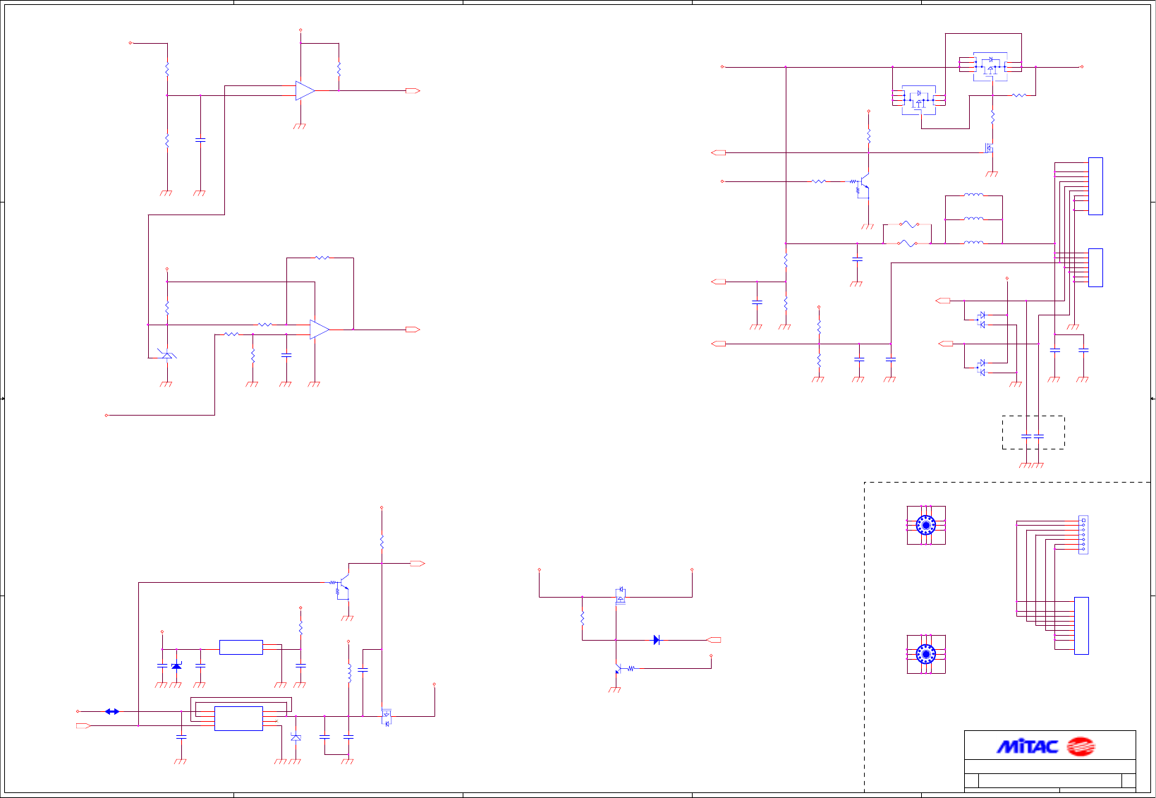
A
A
B
B
C
C
D
D
E
E
4 4
3 3
2 2
1 1
5V Resume Power
Don't Stuff
3V Resume Power
411671200001 02
BATTERY CONNECTOR & 3V,5V-RESUME POWER
20 22Friday, December 28, 2001
C
Title
Size Document
Number
Rev
Date: Sheet of
-ADEN
DVMAIN
BATT_DEAD
-ADEN
BAT_C
BAT_V
BAT_T
SW_+5V A
DBATT
DBATT
LI_OVP
+5VA
+3V
+5VA +5VAS
+5VAS
+5VAS
+5VA
+5VAS
+5VA
+3V_ICH
DVMAIN
DVMAIN
ADINP
+5V
+5V
DBATT
DBATT
ALWAYS
+5VA
J29
R/A-7P/2.5MM/NA
SUYIN
250005MR07G100ZU
1
2
3
4
5
6
7
PD7
UDZS5.1B
SOD323
A K
PC35
47P_NA
0603
12
PR564
475K
0603
1%
12
PL9
120Z/100M 2012
1 2
MTG27
ID2.8/OD7.6
4
5
6
7
9
10
1
2
3
8
11
12
PD508
BAV99/NA
1
2
3
PD507
BAV99/NA
1
2
3
PC22
0.1U
50V
0603
12
PR570
12.1k
0603
1%
1 2
PR572
4.7K
0603
1%
12
PR563
100K
0603
12
PC34
1000P
0603
12
PC31
1000P
0603
12
PC25
0.1U
50V
0603
12
PC32
0.01U
0603
12
J28
7P/2.5MM/H4
CEN
SB-07A-4.0-A2
1
2
3
4
5
6
7
1
2
3
4
5
6
7
PL11
120Z/100M 2012
1 2
PL10
120Z/100M 2012
1 2
PF2
6.5A/32VDC
1 2
D
SG
PQ512
AO3401
G
DS
PC30
0.1U
50V
0603
12
D
S
PQ508
2N7002
G
DS
PR562
301K
0603
1%
12
J33
11P/2.5MM/H3/NA
CEN
BPH-S-11-G-J1A
1
4
5
6
7
8
9
3
11
1
4
5
6
7
8
9
3
11
PR18
4.99K
0603
1%
12
PR561
169K
0603
1%
1 2
R1
PQ511
DTC144TKA
2
1
3
PR16
470K
0603
12
G
D
S
PU10
SI4835DY
SO8
8
7
6
4
5 1
3
2
+
-
PU513A
LMV393M
SSOP8
3
21
84
D8
RLZ3.6B
A K
PU8
TC55RP3302EMB
SOT89N
23 1
VINVOUT GND
PC24
10U
10V
1206
12
PQ2
DTC144WK
1
2
3
PR569
1M
0603
1%
1 2
G
D
S
PU11
SI4835DY
SO8
8
7
6
4
5 1
3
2
D
SG
PQ1
AO3401
G
DS
PR573
100K
0603
12
PR559
100K
0603
1 2
PC555
0.1U
50V
0603
12
J30
11P/2.5MM/H3/NA
CEN
BPH-S-11-G-J1A
1
4
5
6
7
8
9
3
11
1
4
5
6
7
8
9
3
11
PQ509
DTC144WK
1
2
3
PR616
0
0805
12
PC21
0.1U
50V
0603
12
PR568
402K
0603
1%
1 2
PL8
120Z/100M
1608
12
PU7
LP2951-02BM
SO8
8
2
7
3
6
1
5
4
IN
SENSE
F/B
SHUTDN
5VTAP
OUT
ERR-
GND
PR554
1M
0603
1 2
PF1
6.5A/32VDC
1 2
PC33
0.1U
50V
0603
12
PR566
100K
0603
1%
12
PR17
20K
0603
1%
12
PC26
0.1U
50V
0603
12
+
-
PU513B
LMV393M
SSOP8
5
67
84
PR565
100K
0603
1%
12
JS7
SHORT-SMT4
1 2
PR571
43.2K
0603
1%
12
PC556
0.1U
50V
0603
12
PR567
100K
0603
12
PC27
4.7U
0805
+80-20%
12
MTG26
ID2.8/OD7.6
4
5
6
7
9
10
1
2
3
8
11
12
PC36
47P_NA
0603
12
PC557
0.1U
50V
0603
12
PD503
BAS32L
A K
PQ510
SCK431LCSK-5
SOT23N
3 2
1
PC29
4.7U
0805
+80-20%
12
-ADEN(19)
BATT_DEAD (19)
SW_+5V A(19)
-ADEN (19)
BAT_D(19)
BAT_C(19)
BAT_V(19)
BAT_T(19)
-SW_+5VA (19)
LI_OVP (22)
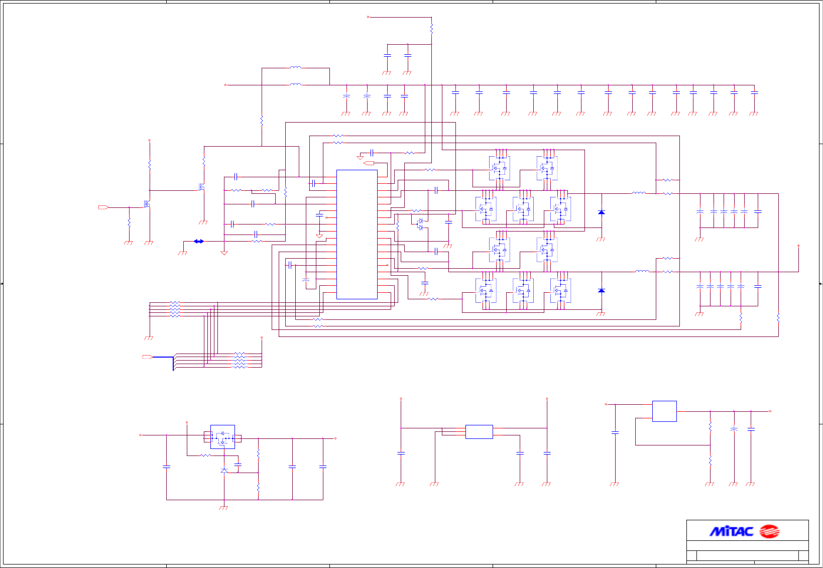
5
5
4
4
3
3
2
2
1
1
D D
C C
B B
A A
02
1.8V,1.5V POWER
411671200001
CPU Vcore/VTT
21 22Friday, December 28, 2001
Title
Size Document
Number
Rev
Date: Sheet of
PVID2
PVID0
PVID4
PVID3
Ith
PVID1
EAIN
RUN/SS
PVID[0..4]
DVMAIN
+3VS
+5VA
CPU_CORE
+5V
+1.5VS
+1.8V_ICH
+3VS
+3V
+1.8VS
+12VS
+3V_ICH
+
PC46
100U
25V
20%
12
PL501
BEAD
0805C
1 2
PR622 0
1 2
PR619 0
1 2
PR21
0
0603
12
PC41
4.7U
0805
+80-20%
12
PC40
0.1U
50V
0603
12
PR620 0
1 2
PR621 0
1 2
PC10
0.1U
50V
0603
12
G
D
S
PU13
AO4400
SO8
8
7
6
4
52
3
1
PL500
BEAD
0805C
1 2
PC42
470P
0603
1 2
PU12
AMS1085
SOT252N
1
2
3
GND/ADJ
VOUT
VIN
PQ3
SCK431LCSK-.5
SOT23N
3 2
1
PC558
4.7U
0805
+80-20%
12
PC45
0.1U
0603
12
PC44
10U
1206
12
PU514
AME8801MEEV
SOT25
1
2
3 4
5
VIN
GND
EN BYP
OUT
PR19
1.2K
0603
1%
12
PC37
4.7U
0805
16V
12
PC560
0.01U
0603
12
PR24
4.7K_1%
0603
12
PR22
1K
0603
1%
12
PR20
560
0603
1%
12
PC524
1000P
PR521
1M
0603
12
PC510
10U
25V
1812
20%
12
PR518 0_NA
PR1
.005
1 2
PD500 BAW56
2
1
3
PR501
0
0603
12
PR514 10
G
D
S
PU507
SI4892DY
SO8
8
7
6
4
5
2
3
1
PC529
0.1U
50V
12
PR4
.003
1 2
PC514
10U
25V
1812
20%
12
PR2
.003
1 2
PC506
10U
25V
1812
20%
12
PR3
.005
1 2
PR527
1K
0603
12
PC523 1000P
PL2
0.7UH
HK-RM136
30%
1 2
PL1
0.7UH
HK-RM136
30%
1 2
+
PC9
100U
6.3V
7343
12
PC501
0.01U
0603
12
G
D
S
PU506
SI4892DY
SO8
8
7
6
4
5
2
3
1
PR513
10K 1%
1 2
PC559
1U
0603
10V
12
PC527
470P
1 2
PR23
4.7K
0603
1 2
PC520 0.1U
PC512
0.1U
50V
0603
12
+
PC3
820U
4V
12
PC43
10U
1206
12
PC500
0.01U
0603
12
PC17
47P
0603
12
D
S
PQ500
2N7002
G
DS
PC519
10U
10V
1206
12
PR528
1M
0603
12
PD1
EC31QS03L
A K
PR519 6.8K
1 2
PR526 10
1 2
G
D
S
PU504
SI4362DY
SO8
8
7
6
4
5
2
3
1
+
PC5
820U
4V
12
PR524 2.7K
1 2
PR515 10
G
D
S
PU505
SI4362DY
SO8
8
7
6
4
5
2
3
1
PR505 10
12
+
PC7
820U
4V
12
PC508
10U
25V
1812
20%
12
+
PC6
820U
4V
12
PC38
0.1U
50V
0603
12
PD2
EC31QS03L
A K
PC518 1U 25V
0805
1 2
PR516
49.9K
0603
1%
12
PC502
10U
25V
1812
20%
12
PR523
15K
0603
1%
1 2
G
D
S
PU502
SI4362DY
SO8
8
7
6
4
5
2
3
1
PC522
1000P
G
D
S
PU501
SI4362DY
SO8
8
7
6
4
5
2
3
1
G
D
S
PU503
SI4892DY
SO8
8
7
6
4
5
2
3
1
PC509
10U
25V
1812
20%
12
G
D
S
PU500
SI4892DY
SO8
8
7
6
4
5
2
3
1
PC504
0.1U
50V
0603
12
PC511
0.1U
50V
0603
12
PC39
0.1U
50V
0603
12
G
D
S
PU2
SI4362DY
SO8
8
7
6
4
5
2
3
1
JS501
SHORT-SMT4
1 2
PR517 0_NA
PC505
10U
25V
1812
20%
12
PR509 0_NA
PC516
0.1U
50V
0603
12
PC503
0.1U
50V
0603
12
PR502
10
0603
12
PC515
0.1U
RP508
10K*4
1206
1
2
3
4
8
7
6
5
PR507 10K
PR520 10
1 2
PR500
0
0603
12
PU508
LTC1709EG-9
SSOP36A
1
2
3
4
6
7
8
9
10
11
12
13
14
15
16
17
18
5
36
35
34
33
32
31
30
29
28
27
26
25
24
23
22
21
20
19
RUNN/SS
SENSE1+
SENSE1-
EAIN
PLLIN
NC0
ITH
SGND
VDIFFOUT
VOS-
VOS+
SENSE2-
SENSE2+
ATTENOUT
ATTENIN
VID0
VID1
PLLFLTR
NC1
TG1
SW1
BOOST1
VIN
BG1
EXTVCC
INTVCC
PGND
BG2
BOOST2
SW2
TG2
PGOOD
VBIAS
VID4
VID3
VID2
G
D
S
PU1
SI4362DY
SO8
8
7
6
4
5
2
3
1
PC513
10U
25V
1812
20%
12
PR508 0_NA
PC507
10U
25V
1812
20%
12
PC521 0.1U
1 2
PR510 0_NA
D
S
PQ501
2N7002
G
DS
PR512
1M
0603
12
PC528 100P
1 2
PC517
10U
25V
1812
20%
12
+
PC47
100U
25V
20%
12
+
PC575
100U
6.3V
7343
12
+
PC574
100U
6.3V
7343
12
+
PC583
100U
6.3V
7343
12
+
PC573
100U
6.3V
7343
12
+
PC572
100U
6.3V
7343
12
+
PC582
100U
6.3V
7343
12
CPU_CORE_EN(5)
PVID[0..4](4)
VRMPWRGD(13)
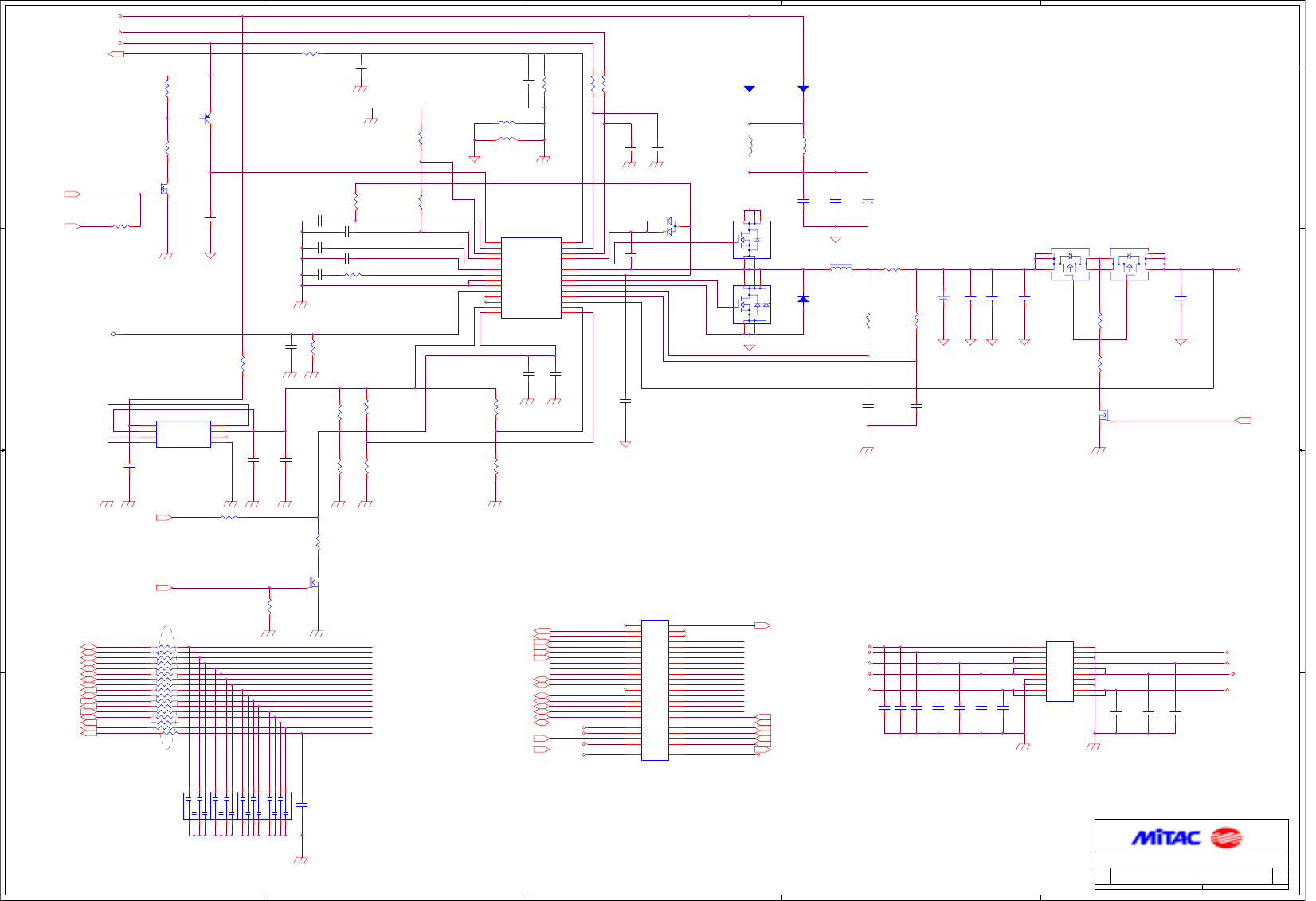
A
A
B
B
C
C
D
D
E
E
4 4
3 3
2 2
1 1
3V Resume Power
R01
411671200001 02
DC-DC CONNECTOR ,CHARGER
22 22Friday, December 28, 2001
C
Title
Size Document
Number
Rev
Date: Sheet of
DVCC3
I_CHG
ADINP_1
DP_LPD7
-DP_ACK
DP_LPD0
-DP_ERR
DP_PE
DP_LPD1
-BATT_R
-DP_INIT
DP_LPD3
BLADJ
-BATT_LED
-DP_SLIN
-DP_STB
DP_BUSY
ENPBLT
DP_SLCT
IRRX
FIRSEL
-AC_POWER
DP_LPD2
-BATT_G
-SUSC
DP_LPD4
-DP_AFD
ADINP_1
DP_LPD5
IRTX
DP_LPD6
LEARNING
PWR_ON
DP_LPD5
P_BUSY
P_LPD5
P_LPD0
-DP_ERR
-P_ERR
DP_LPD0
-DP_SLIN
-DP_STB
-P_SLIN
P_LPD4 DP_LPD4
-DP_AFD
P_SLCT
-DP_INIT
-P_INIT
DP_LPD6
DP_PE
DP_LPD2
DP_SLCT
-P_AFD
P_LPD6
DP_LPD7
-DP_ACK
-P_STB
P_PE
P_LPD2
-P_ACK
DP_LPD3
P_LPD7
DP_BUSY
DP_LPD1
P_LPD1
P_LPD3
ADINP
ADINP_2
ADINP
ADINP_2
+5VS
+3VS
+5VS
+5V
+3V
+12V
+5VAS
+12VS
DVMAIN DVMAIN
ALWAYS
ADINP_1
ADINP_2
ADINP
ADINP_1
ADINP_2
ADINP
DBATT
PL15 BEAD 0805C
1 2
PL14 BEAD 0805C
1 2
PR537
1M
0603
1%
12
PR533
15K_NA
0603
1%
12
PR536
10K
0603
1%
12
PC565
0.1U
50V
0603
12
PR539
1K
0603
1%
1 2
PC564
10U
10V
1206
12
PR558
1K
0603
1%
12
D
S
PQ504
2N7002_NA
G
DS
PR535
100K
0603
1%
12
PR615
0
0603
1 2
PD6
EC31QS03L
A K
G
D
S
PU9
SI4835DY
SO8
8
7
6
4
51
3
2
J3
HDR/10PX2/H8.4
CEN
PH/PS-D-RA-44-X-X
1
3
5
7
9
11
13
15
17
19
2
4
6
8
10
12
14
16
18
20
RP504
0*4_DFS
1206
1
2
3
4
8
7
6
5
PR560
100K
0603
1%
12
C6
0.1U
50V
0603
12
RP503
0*4_DFS
1206
1
2
3
4
8
7
6
5
PC552
0.1U
50V
0603
12
PC19
0.1U
50V
0603
12
PR556
100K
0603
12
PR541
100K
0603
1%
12
PC28
10U
25V
1206
12
PR534
100K
0603
1%
12
PC543
0.1U
50V
0603
12
PR557
33
12
PC547
0.1U
50V
0603
1 2
C519
0.1U
50V
0603
12
PL7
10uH
1 2
PL5
BEAD
0805C
12
+
PC18
100U
25V
20%
12
CP504
22P*4
1206
1
2
3
4
8
7
6
5
PR550 1K
1 2
C2
0.1U
50V
0603
12
J6
FM/22PX2/1.27
B06P-0110-441
SPEED
1
3
5
7
9
11
13
15
17
19
21
23
25
27
29
31
33
35
37
39
41
43
2
4
6
8
10
12
14
16
18
20
22
24
26
28
30
32
34
36
38
40
42
44 4546 4748 4950
1
3
5
7
9
11
13
15
17
19
21
23
25
27
29
31
33
35
37
39
41
43
2
4
6
8
10
12
14
16
18
20
22
24
26
28
30
32
34
36
38
40
42
44 4546 4748 4950
PD4
EC31QS03L
AK
PC539
0.1U
50V
0603
12
CP503
22P*4
1206
1
2
3
4
8
7
6
5
CP505
22P*4
1206
1
2
3
4
8
7
6
5
RP500
0*4_DFS
1206
1
2
3
4
8
7
6
5
D
S
PQ507
2N7002 G
DS
PC20
10U
25V
1206
12
PC2
22U
10V
1210
12
G
D
S
PU6
SI4832DY
SO8
8
7
6
4
5
2
3
1
PC549 0.01U
1 2
PQ505
MMBT3906L
BE
C
PC550 0.01U
1 2
PD5
EC31QS03L
AK
G
D
S
PU5
AO4400
SO8
8
7
6
4
5
2
3
1
PR546
10K
C509
0.1U
50V
0603
12
PR543
1M_NA
0603
12
PU511
MAX1772
QSOP28
1
2
3
4
5
6
7
8
9
10
11
12
13
14
28
27
26
25
24
23
22
21
20
19
18
17
16
15
DCIN
LD0
CLS
REF
CCS
CCI
CCV
GND0
GND1
ICHG
ACIN
ACOK
REFIN
ICTL
IINP
CSSP
CSSN
BST
DHI
LX
DL0V
DL0
PGND
CSIP
CSIN
BATT
CELLS
VCTL
PC541
10U
25V
1206
12
TP542 1
PR542
49.9K
0603
1%
12
PR548
10
1 2
R500 0_DFS
0603 1 2
PR532
10
0603
12
C716
0.1U
50V
0603
12
PC546
1U
25V
0805
1 2
PR552
10
1 2
PC542
0.1U
PR549
15K
0603
1%
12
PR547
33K
0603
12
C520
0.1U
50V
0603
12
PL6
BEAD
0805C
12
PC537
0.1U
50V
0603
12
PC548
1U
25V
0805
1 2
PU510
LP2951-3.3BM
SO8
8
2
7
3
6
1
5
4
IN
SENSE
F/B
SHUTDN
5VTAP
OUT
ERR-
GND
PC553
1U
1 2
CP502
22P*4
1206
1
2
3
4
8
7
6
5
PC535
4.7U
0805
+80-20%
12
PC1
10U
10V
1206
12
C504
22P
0603
5%
12
PC540
0.1U
50V
0603
12
PC536
0.1U
50V
0603
12
PC544
10U
25V
1206
12
PR14
1
0603
12
+
PC23
100U
25V
20%
12
PR13
.035
2512
5%
1 2
PR553
47K
0603
1 2
C511
0.1U
50V
0603
12
D
S
PQ506
2N7002
G
DS
PC538
0.1U
50V
0603
12
G
D
S
PU512
SI4835DY
SO8
8
7
6
4
5 1
3
2
PC551 1U
1 2
PC554 10U 10V
1 2
PD502BAW56
2
13
C5
0.1U
50V
0603
12
PR15
1
0603
12
PR551
1M
0603
12
PC545
0.1U
50V
0603
12
RP502
0*4_DFS
1206
1
2
3
4
8
7
6
5
PR555
12.1k
0603
1%
12
PC563
10U
10V
1206
12
I_LIMIT(19)
LI_OVP (20)
LI_OVP(20)
CHARGING(19)
-USBOC0(13)
USBP0_0-(13)
-SUSB(13,15,19)
ENPBLT (10)
TV_CRMA(10)
-BATT_R (12)
USBP2_2-(13)
-USBOC2(13)
IRRX(18)
-BATT_G (12)
FIRSEL(18)
-AC_POWER (12)
TV_LUMA(10)
PWR_ON (19)
-BATT_LED (12)
LEARNING (19)
-SUSC(13,19)
USBP0_0+(13)
TV_COMP(10)
BLADJ(19)
USBP2_2+(13)
CSYNC(10)
IRTX(18)
-P_ACK(18)
P_LPD4(18)
P_LPD0(18)
P_PE(18)
P_BUSY(18)
-P_STB(18)
-P_ERR(18)
P_LPD5(18)
-P_SLIN(18)
-P_AFD(18)
P_SLCT(18)
P_LPD1(18)
P_LPD3(18)
-P_INIT(18)
P_LPD6(18)
P_LPD2(18)
P_LPD7(18)
CHG_I(19)
PWR_ON(19)
-LID (19)
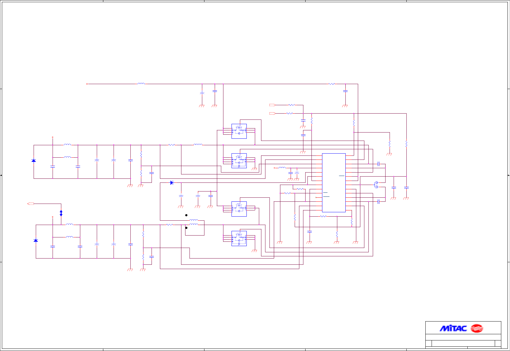
5
5
4
4
3
3
2
2
1
1
D D
C C
B B
A A
SYSTEM POWER (5V 3V 12V)
411671200004 0A
SYSTEM POWER
13Monday, October 22, 2001
Title
Size Document
Number
Rev
Date: Sheet of
I4
DVMAIN
I5
I6
A4
I3
B3
D2
BKL_VMAIN
A5
A2
+5V
+12V
+3V
DVMAIN
PR503
0
1 2
PR505 0
1 2
PR2
0
0603
1 2
PC20
470P
0603
10%
12
PR16
100K
0603
1%
12
PR15
37.4K
0603
1%
12
PC513
0.1U
50V
0603
12
PD502
BAW56
2
1
3
PC502
0.1U
50V
0603
12
PC503
0.1U
50V
0603
12
PC12
0.1U
50V
0603
12
PC516
0.1U
50V
0603
12
PC504
0.1U
50V
0603
12
PD504
EC10QS03L
A K
PT1
10UH
IND_CDRH125B
1 3
2 4
PC6
0.1U
50V
0603
12
PL504
BEAD
0805C
1 2
PR1
.015
2512
1%
1 2
PR8
.015
2512
1%
1 2
PR18
97.6K_NA
0603
1%
12
PR17
100K_NA
0603
1%
12
PC21
470P_NA
0603
10%
12
+
PC9
100U
25V
12
+
PC5
100U
25V
12
+
PC4
100U
25V
12
+
PC11
100U
25V
12
PL1
10UH
CDRH127-100MC
1 2
PC16
0.1U
50V
0603
12
JS501
SHORT-SMT3
12
+
PC1
100U/H2.8
10V
7343
12
+
PC7
330U
7343
4V
12
PR504 0/NA 0603
1 2
PR511
1K
0603
12
PR3
1K
0603
12
PL2
BEAD
0805C
1 2
PR12
1M
0603
12
PR510
0_NA
0603
1 2
PU1
MAX1632 SSOP28A
21
27
25
26
24
20
1
2
3
11
15
9
8
6
10
12
22
23
28
7
14
13
4
5
18
16
17
19
VL
DH3
BST3
LX3
DL3
PGND
CSH3
CSL3
FB3
RESET
SEQ
REF
GND
SYNC
SKIP
FB5
V+
SHDN
RUN/ON3
TIME/ON5
CSH5
CSL5
12OUT
VDD
BST5
DH5
LX5
DL5
PC2
1U
0603
12
PR509
10 0603
1 2
G
D
S
PU502
SI4832DY
SO8
8
7
6
4
52
3
1
PR501
0_NA
12
PR508
0_NA
0603
12
PD503
EC10QS03L
A K
PL3
BEAD
0805C
1 2
G
D
S
PU503 SI4800DY
SO8
8
7
6
4
52
3
1
PL501
BEAD
0805C
1 2
G
D
S
PU506
SI4800DY
SO8
8
7
6
4
52
3
1
PR502
0_NA
12
PC13
0.1U
50V
0603
12
PC515
0.1U
50V
0603
12
PC14
0.1U
50V
0603
12
PC511
4.7U
16V
1206
12
PL506
BEAD 0805C
1 2
PC15
0.1U
50V
0603
12
PC512
470P_NA
0603
10%
12
G
D
S
PU505
SI4832DY
SO8
8
7
6
4
52
3
1
+
PC8
100U/H2.8
10V
7343
12
PC514
4.7U
16V
1206
12
PC501
4.7U
16V
1206
12
+
PC3
100U/H2.8
10V
7343
12
PL507
BEAD 0805C
1 2
PR19 0
1 2
PD1
EC11FS2
DC2010
A K
-SUSC(2)
BKL_VMAIN(2)
PWR_ON(2)
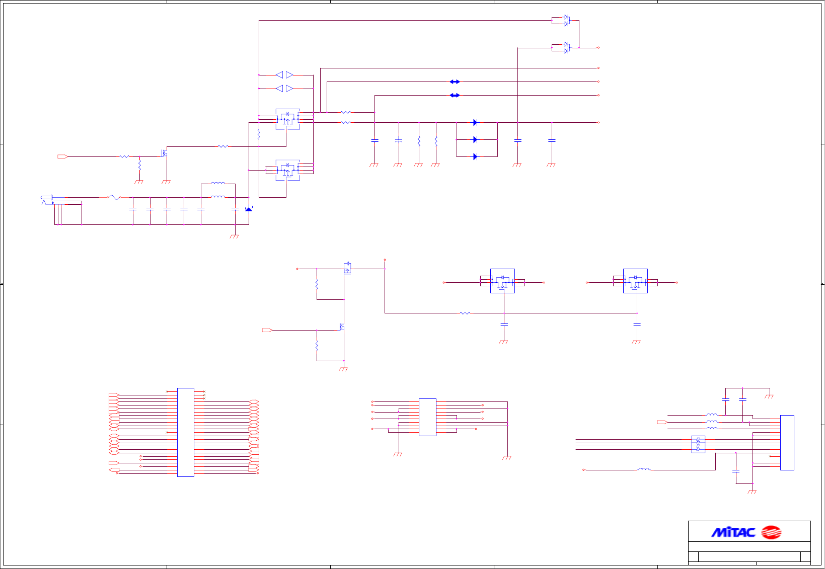
5
5
4
4
3
3
2
2
1
1
D D
C C
B B
A A
Inverter
Note : BKL_VMAIN is Power Trace
411671200004 0A
DC POWER
23Monday, October 22, 2001
Title
Size Document
Number
Rev
Date: Sheet of
DVMAIN
L3
LEARNING
L1
BLADJ
BKL_VMAIN
P_LPD2
P_LPD4
FIRSEL
-BATT_R
P_PE
-P_ACK
-P_AFD
P_LPD1
-AC_POWER
P_LPD7
P_LPD6
P_BUSY ENPBLT1
P_SLCT
-BATT_LED
P_LPD5
-P_STB
-P_ERR
IRTX
-P_SLIN
-P_INIT
LEARNING
-BATT_G
P_LPD0
IRRX
ENPBLT1
P_LPD3
L2
-SUSC
PWR_ON
-USBOC0
-USBOC2
USBP0_0-
USBP0_0+
USBP2_2+
USBP2_2-
ADINP
ALWAYS
ADINP_1
-SUSB
ADINP_2
-AC_POWER
-BATT_G
-BATT_LED
-BATT_R
-SUSB
+12VS
+5VAS
+12V
+3V
+3VS
+5VS
+5V
+5V +3V+5VS +3VS
DVMAIN
ADINP_2
ADINP_1
ALWAYS
ADINP
DVMAIN
ADINP
ALWAYS
DVMAIN
ADINP_1ADINP_2
+5VAS
+5VS
+12V
+12VS
PC506
0.1U
50V
0603
12
PC509
0.1U
50V
12
PC507
0.1U
50V
0603
12
+
PC19
100U
25V
12
PC17
0.1U
50V
0603
12
PC18
1000P
0603
12
JO503
OPEN-SMT4
1 2
PC508
0.1U
50V
0603
12
PR9
47K
0603
1 2
PJ2
MA/22PX2/1.27
SPEED
G442-8701-441
1
3
5
7
9
11
13
15
17
19
2
4
6
8
10
12
14
16
18
20 21
23
25
27
29
31
33
35
37
39
41
43
22
24
26
28
30
32
34
36
38
40
42
44 4546 4748 4950
1
3
5
7
9
11
13
15
17
19
2
4
6
8
10
12
14
16
18
20 21
23
25
27
29
31
33
35
37
39
41
43
22
24
26
28
30
32
34
36
38
40
42
44 4546 4748 4950
PD5
EC31QS03L
A K
PR10
10K
0603
12
PR4
470K
0603
1 2
PR513
.1
1 2
PR514
.1
1 2
PD4
EC31QS03L
A K
PD3
BAV70LT1
1
23
PD2
BAV70LT1
1
23
G
D
S
PQ502
SI4835DY
SO8
8
7
6
4
51
3
2
PR5
470K
0603
1 2
FA501
120OHM/100MHZ
1
2
3
4 5
6
7
8
PR6
100K
0603
12
D
S
PQ3
2N7002
G
DS
JL3 SHORT-SMT4
1 2
JL2
SHORT-SMT4
1 2
PR7
1M
0603
12
D
SG
PQ2
SI2301DS
G
DS
PR515
1M
0603
12
PC517
0.1U
50V
0603
12
J6
MA/12PX1/ST
SPEED
Y17-101-0001
1
2
3
4
5
6
7
8
9
10
11
12
GND1
GND2
1
2
3
4
5
6
7
8
9
10
11
12
GND1
GND2
PC518
0.1U
50V
0603
12
PF501 6.5A/32VDC
1 2
PR506
470K
0603
1 2
PC10
0.1U
50V
0603
12
PJ1
HDR/10PX2/H8.49
CEN
PH-D-RA-44-X-X
1
3
5
7
9
11
13
15
17
19
2
4
6
8
10
12
14
16
18
20
G
D
S
PU501
AO4400
SO8
8
7
6
4
52
3
1
C512
0.1U
50V
0603
12
J5
JACK-3P
2DC-S315-X03
3
2
1
4
5
6
L509 BEAD
0805C
1 2
L507
BEAD
0805C
1 2
L508 BEAD
0603B
1 2
L510 BEAD
0603B
1 2
JO502
OPEN-SMT4
1 2
PR11
10K
0603
12
C513
0.1U
50V
0603
12
C514
0.1U_NA
50V
0603
12
PD6
EC31QS03L
A K
PC510
0.1U
50V
0603
12
D
S
PQ1
2N7002
SOT23_FET
G
DS
PC505
1U
25V
0805
12
PL503
120Z/100M
2012
1 2
PL502 120Z/100M 2012
1 2
PD501
RLZ24D
A K
G
D
S
PQ503
SI4835DY
SO8
8
7
6
4
51
3
2
G
D
S
PU504
AO4400
SO8
8
7
6
4
52
3
1
LEARNING
BKL_VMAIN(1)
P_LPD5 (3)
-AC_POWER
P_LPD7 (3)
-P_ACK(3)
-P_INIT (3)
IRRX(3)
-P_AFD (3)
LEARNING
P_LPD1 (3)
P_PE(3)
P_LPD2 (3)
-P_ERR (3)
P_LPD0 (3)
-BATT_R
P_LPD6 (3)
P_SLCT (3)
P_LPD4 (3)
IRTX(3)
-BATT_LED
P_LPD3 (3)
ENPBLT1
-P_SLIN (3)
FIRSEL(3)
-P_STB (3)
P_BUSY(3)
BLADJ
-BATT_G
TV_CRMA(3)
TV_COMP(3)
CSYNC(3)
TV_LUMA(3)
-SUSC(1)
PWR_ON (1)
-USBOC0(3)
-USBOC2(3)
USBP0_0+(3) USBP0_0-(3)
USBP2_2+(3) USBP2_2-(3)
-SUSB
-SUSB
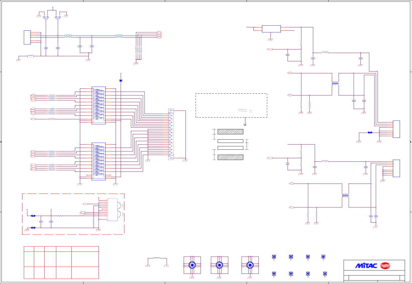
5
5
4
4
3
3
2
2
1
1
D D
C C
B B
A A
GND_IO2
GND_IO2 GND_IO2
GND_IO2
Parallel Port Connector
FIR Module
FIR
IR Mode Select
HI
LOW
HI
IRMODE1
1/3 Distance Power
Full Distance Power
MIR/FIR
LOW
LOW
HI
HIHI
X
IRMODE0
LOW HI
Full Distance Power
HI
1/3 Distance Power
SIR
FIRSEL
LOW
LOW MIR/FIRLOW
TX Function
HI
Shutdown
2/3 Distance PowerLOW
HI MIR/FIR
LOW
HI
2/3 Distance Power
Shutdown
IR Mode Select
RX Function
SIR
LOW
GND_IO2
GND_FIR
TV OUT
GND_TV
GND_TV
GND_USB
USBP+
only use one fuse.
GND_USB
GND_USB
USBP-
GND_USB
5mil
Layout note:
Place two fuses on same location,
GND_USB
GND_USB
Same legth
10mil
5mil
GND
USBP0+
10mil
10mil
USBP0-
GND
10mil
5mil
411671200004 0A
DC POWER
33Monday, October 22, 2001
Title
Size Document
Number
Rev
Date: Sheet of
-PP_AFD
P_LPD0
LPD4
INIT#
P_LPD3
BUSY
LPD7
PP_SLCT
LPD1
P_PE
ACK#
P_LPD5 PP_LPD6
-P_SLIN
-P_ERR
-PP_INIT
-PP_SLIN
AFD#
SLCT
-PP_STB
LPD3
ERR#
-P_INIT
PP_LPD5
PP_PE
P_LPD4
LPD6
-P_ACK
P_LPD2
-PP_ERR
PP_LPD3
SLIN#
P_LPD6
PP_LPD0
PP_BUSY
P_LPD7 PP_LPD7
P_LPD1
-P_STB
-P_AFD
PP_LPD2
LPD5
STB#
LPD0
PP_LPD1
P_SLCT
PE
PP_LPD4
LPD2
-PP_ACK
P_BUSY
IRTX
FIRSEL
IRRX
TV_CRMA
TV_LUMA
-USBOC2
USB2VCC5
-USBOC0
USB0VCC5
USB0VCC5
+5VS
+3VS VCC3_IR
VCC3_IR
+3V
+5V
C505
100P
0603
10%
12
C503
100P
0603
10%
12
L503
120Z/100M
1608
1 2
C506
100P
0603
10%
12
FD3
FIDUCIAL-MARK
1
FD1
FIDUCIAL-MARK
1
L504
120Z/100M
1608
1 2
FD502
FIDUCIAL-MARK
1
C504
100P
0603
10%
12
FD504
FIDUCIAL-MARK
1
FD503
FIDUCIAL-MARK
1
FD501
FIDUCIAL-MARK
1
FD2
FIDUCIAL-MARK
1
FD4
FIDUCIAL-MARK
1
RP501
75*4
1206
1
2
3
4
8
7
6
5
D502
BAV99
1
2
3
D503
BAV99
1
2
3
JL501
SHORT-SMT4
1 2
RP10*4
1206
1
2
3
4
8
7
6
5
J1
PIO
SUYIN
7536S-25G2T
1
14
2
15
3
16
4
17
5
18
6
19
7
20
8
21
9
22
10
23
11
24
12
25
13
26
27
L501
120Z/100M
2012
1 2
JL1
SHORT-SMT4
1 2
J4
MINI-DIN/4P
C10801-10405
1
2
3
4
GND1
GND2
1
2
3
4
GND1
GND2
C515
10U_NA
16V
1206
12
R501 2.7
2010 1%
1 2
D501
BAS32L
AK
U502
PAC128401Q
QSOP24A
21
1
20
19
222
18
17
3
24
16
23
4
15
5
14
6
13
7
8
9
10
11
12
U501
PAC128401Q
QSOP24A
21
1
20
19
222
18
17
3
24
16
23
4
15
5
14
6
13
7
8
9
10
11
12
L5
JP_BEAD_DFS
1 2
C507
0.1U
50V
0603
12
U1
HSDL-3600
1
2
3
4
5
6
7
8
9
10
11
VCC
AGND
FIR_SEL
MD0
MD1
NC
GND
RXD
TXD
LEDA
GND1
RP20*4
1206
1
2
3
4
8
7
6
5
U2
RT9701-CBL
SOT25
1
2
3
4 5
VOUT0
GND
VIN0
VIN1 VOUT1
L3
600Z/100M
CORE_ACM2520U
1
4
2
3
C511
47P/NA
0603
12
C510
47P/NA
0603
12
R503
15K
0603
12
R502
15K
0603
12
L2
200Z/100M
CORE_ACM2520U
1
4
2
3
C3
10U_NA
10V
1206
12
MTG1
ID2.8/OD7.6
4
5
6
7
9
10
1
2
3
8
11
12
C4
1000P
0603
12
R505
15K
0603
12
L4
120Z/100M
2012
1 2
R3
47K
0603
12
C502
0.1U
50V
0603
12
R5
33K
0603
12
R4
33K
0603
12
C1
1000P
0603
12
R1
00603
1 2
L1
120Z/100M
2012
1 2
J3
USB/4PX1
LINKTEK
UAR80-4W510
1
2
3
4
GND1
GND2
GND3
GND4
1
2
3
4
GND1
GND2
GND3
GND4
JO501
SHORT-SMT4
1 2
R6
47K
0603
12
C2
10U_NA
10V
1206
12
J2
USB/4PX1
LINKTEK
UAR80-4W510
1
2
3
4
GND1
GND2
GND3
GND4
1
2
3
4
GND1
GND2
GND3
GND4
R504
15K
0603
12
C508
47P/NA
0603
12
RP40*4
1206
1
2
3
4
8
7
6
5
C501
0.1U
50V
0603
12
RP30*4
1206
1
2
3
4
8
7
6
5
L505
120Z/100M
1608
1 2
L502
120Z/100M
1608
1 2
C509
47P/NA
0603
12
MTG2
ID2.8/OD7.6
4
5
6
7
9
10
1
2
3
8
11
12
R2
0_DFS
0603
1 2
MTG3
ID2.8/OD7.6
4
5
6
7
9
10
1
2
3
8
11
12
-P_INIT(2)
P_LPD3(2)
P_LPD5(2)
P_LPD7(2)
P_SLCT(2)
-P_ACK(2)
P_LPD2(2)
-P_STB(2)
P_LPD0(2)
P_BUSY(2)
P_LPD4(2)
-P_AFD(2)
P_LPD6(2)
P_LPD1(2)
-P_ERR(2)
P_PE(2)
-P_SLIN(2)
IRTX(2) IRRX(2)
FIRSEL(2)
CSYNC (2)
TV_CRMA (2)
TV_LUMA (2)
TV_COMP (2)
-USBOC2(2)
-USBOC0(2)
USBP0_0+(2)
USBP0_0-(2)
USBP2_2+(2)
USBP2_2-(2)

Reference Material
Reference Material
Intel Pentium 4 Processor mFC-PGA2 478Pin
INTEL 82845 Memory Controller Hub
INTEL 82801BA I/O Controller Hub
PCI4410 Manual-PC Card and OHCI Controller
Frequency Generator ICS950805
Intel. INC
Intel. INC
Intel. INC
CHRONTEL. INC
ICS. INC
Engineer Hardware Specification Technology.Corp/MiTAC
Engineer Software Specification Technology.Corp/MiTAC

SERVICE MANUAL FOR 8170
SERVICE MANUAL FOR
SERVICE MANUAL FOR 8170
Sponsoring Editor : Jesse Jan
Author : Jacey Liu
Assistant Editor : Janne Liu
Publisher : MiTAC International Corp.
Address : 1, R&D Road 2, Hsinchu Science-Based Industrial, Hsinchu, Taiwan, R.O.C.
Tel : 886-3-5779250 Fax : 886-3-5781245
First Edition : Feb. 2002
E-mail : Willy.Chen @ mic.com.tw
Web : http: //www.mitac.com http: //www.mitacservice.com
