Mitsubishi Electronics Digital Electronic Accessory Q02Cpu Users Manual User's Manual(Hardware Design, Maintenance And Inspection)
Q25HCPU to the manual e7e2857b-a9d1-4d46-b589-dcd5cdeee88e
2015-02-09
: Mitsubishi-Electronics Mitsubishi-Electronics-Mitsubishi-Digital-Electronics-Electronic-Accessory-Q02Cpu-Users-Manual-556612 mitsubishi-electronics-mitsubishi-digital-electronics-electronic-accessory-q02cpu-users-manual-556612 mitsubishi-electronics pdf
Open the PDF directly: View PDF ![]() .
.
Page Count: 236 [warning: Documents this large are best viewed by clicking the View PDF Link!]
- COVER
- SAFETY PRECAUTIONS
- REVISIONS
- INTRODUCTION
- CONTENTS
- About Manuals
- How to Use This Manual
- About the Generic Terms and Abbreviations
- 1 OVERVIEW
- 2 SYSTEM CONFIGURATION FOR SINGLE CPU SYSTEM
- 3 GENERAL SPECIFICATIONS
- 4 HARDWARE SPECIFICATION OF THE CPU MODULE
- 5 POWER SUPPLY MODULE
- 6 BASE UNIT AND EXTENSION CABLE
- 7 MEMORY CARD AND BATTERY
- 8 EMC AND LOW VOLTAGE DIRECTIVE
- 9 LOADING AND INSTALLATION
- 10 MAINTENANCE AND INSPECTION
- 11 TROUBLESHOOTING
- 11.1 Troubleshooting Basics
- 11.2 Troubleshooting
- 11.2.1 Troubleshooting flowchart
- 11.2.2 Flowchart for when the "MODE" LED is not turned on
- 11.2.3 Flowchart for when the "MODE" LED is flickering
- 11.2.4 Flowchart for when the "POWER" LED is turned off
- 11.2.5 Flowchart for when the "RUN" LED is turned off
- 11.2.6 When the "RUN" LED is flickering
- 11.2.7 Flowchart for when the "ERR." LED is on/flickering
- 11.2.8 When the "USER" LED is turned on
- 11.2.9 When the "BAT." LED is turned on
- 11.2.10 Flowchart for when the "BOOT" LED is flickering
- 11.2.11 Flowchart for when output module LED is not turned on
- 11.2.12 Flowchart for when output load of output module does not turn on
- 11.2.13 Flowchart for when unable to read a program
- 11.2.14 Flowchart for when unable to write a program
- 11.2.15 Flowchart for when it is unable to perform boot operation from memory card
- 11.2.16 Flowchart for when UNIT VERIFY ERR. occurs
- 11.2.17 Flowchart for when CONTROL BUS ERR. occurs
- 11.3 Error Code List
- 11.4 Canceling of Errors
- 11.5 I/O Module Troubleshooting
- 11.6 Special Relay List
- 11.7 Special Register List
- APPENDICES
- INDEX
- WARRANTY

MELSEC System Q
Programmable Logic Controllers
User’s Manual
High Performance Model QCPU
Q02CPU, Q02HCPU,
Q06HCPU, Q12HCPU,
Q25HCPU
INDUSTRIAL AUTOMATION
MIT
SU
BI
S
HI ELE
C
TRI
C
MIT
SU
BI
S
HI ELE
C
TRI
C
Art. no.: 130000
01 10 2002
SH (NA)-080037-F
A - 1 A - 1
SAFETY PRECAUTIONS
(Read these precautions before using.)
When using Mitsubishi equipment, thoroughly read this manual and the associated manuals introduced in
this manual. Also pay careful attention to safety and handle the module properly.
These SAFETY PRECAUTIONS classify the safety precautions into two categories: "DANGER" and
"CAUTION".
!DANGER
CAUTION
!
Indicates that incorrect handling may cause hazardous conditions,
resulting in death or severe injury.
Indicates that incorrect handling may cause hazardous conditions,
resulting in medium or slight personal injury or physical damage.
Depending on circumstances, procedures indicated by ! CAUTION may also be linked to serious
results.
In any case, it is important to follow the directions for usage.
Store this manual in a safe place so that you can take it out and read it whenever necessary. Always
forward it to the end user.
[DESIGN PRECAUTIONS]
! DANGER
Install a safety circuit external to the PLC that keeps the entire system safe even when there
are problems with the external power supply or the PLC module. Otherwise, trouble could result
from erroneous output or erroneous operation.
(1) Outside the PLC, construct mechanical damage preventing interlock circuits such as
emergency stop, protective circuits, positioning upper and lower limits switches and
interlocking forward/reverse operations.
(2) When the PLC detects the following problems, it will stop calculation and turn off all output
in the case of (a). In the case of (b), it will stop calculation and hold or turn off all output
according to the parameter setting.
Note that the AnS series module will turn off the output in either of cases (a) and (b).
(a) The power supply module has over current protection equipment and over voltage
protection equipment.
(b) The PLC CPUs self-diagnosis functions, such as the watch dog timer error, detect
problems.
In addition, all output will be turned on when there are problems that the PLC CPU cannot
detect, such as in the I/O controller. Build a fail safe circuit exterior to the PLC that will make
sure the equipment operates safely at such times. See section 9.1 of this manual for
example fail safe circuits.
(3) Output could be left on or off when there is trouble in the outputs module relay or transistor.
So build an external monitoring circuit that will monitor any single outputs that could cause
serious trouble.
A - 2 A - 2
[DESIGN PRECAUTIONS]
! DANGER
When overcurrent which exceeds the rating or caused by short-circuited load flows in the output
module for a long time, it may cause smoke or fire. To prevent this, configure an external safety
circuit, such as fuse.
Build a circuit that turns on the external power supply when the PLC main module power is
turned on. If the external power supply is turned on first, it could result in erroneous output or
erroneous operation.
When there are communication problems with the data link, refer to the corresponding data link
manual for the operating status of each station. Not doing so could result in erroneous output or
erroneous operation.
When connecting a peripheral device to the CPU module or connecting a personal computer or
the like to the intelligent function module to exercise control (data change) on the running PLC,
configure up an interlock circuit in the sequence program to ensure that the whole system will
always operate safely.
Also before exercising other control (program change, operating status change (status control))
on the running PLC, read the manual carefully and fully confirm safety.
Especially for the above control on the remote PLC from an external device, an immediate
action may not be taken for PLC trouble due to a data communication fault.
In addition to configuring up the interlock circuit in the sequence program, corrective and other
actions to be taken as a system for the occurrence of a data communication fault should be
predetermined between the external device and PLC CPU.
! CAUTION
Do not bunch the control wires or communication cables with the main circuit or power wires, or
install them close to each other. They should be installed 100 mm (3.94 inch) or more from
each other. Not doing so could result in noise that would cause erroneous operation.
When controlling items like lamp load, heater or solenoid valve using an output module, large
current (approximately ten times greater than that present in normal circumstances) may flow
when the output is turned OFF to ON.
Take measures such as replacing the module with one having sufficient rated current.
A - 3 A - 3
[INSTALLATION PRECAUTIONS]
! CAUTION
Use the PLC in an environment that meets the general specifications contained in this manual.
Using this PLC in an environment outside the range of the general specifications could result in
electric shock, fire, erroneous operation, and damage to or deterioration of the product.
Hold down the module loading lever at the module bottom, and securely insert the module
fixing latch into the fixing hole in the base unit.
Incorrect loading of the module can cause a malfunction, failure or drop.
When using the PLC in the environment of much vibration, tighten the module with a screw.
Tighten the screw in the specified torque range. Undertightening can cause a drop, short circuit
or malfunction. Overtightening can cause a drop, short circuit or malfunction due to damage to
the screw or module.
When installing extension cables, be sure that the connectors of base unit are installed
correctly. After installation, check them for looseness. Poor connections could cause an input or
output failure.
Securely load the memory card into the memory card loading connector. After loading, check
for lifting. Lifting can cause a malfunction due to a contact fault.
Completely turn off the external power supply before loading or unloading the module. Not
doing so could result in electric shock or damage to the product.
Do not directly touch the module's conductive parts or electronic components. Touching the
conductive parts could cause an operation failure or give damage to the module.
[WIRING PRECAUTIONS]
! DANGER
Completely turn off the external power supply when installing or placing wiring. Not completely
turning off all power could result in electric shock or damage to the product.
When turning on the power supply or operating the module after installation or wiring work, be
sure that the module's terminal covers are correctly attached. Not attaching the terminal cover
could result in electric shock.
A - 4 A - 4
[WIRING PRECAUTIONS]
! CAUTION
Be sure to ground the FG terminals and LG terminals to the protective ground conductor. Not
doing so could result in electric shock or erroneous operation.
When wiring in the PLC, be sure that it is done correctly by checking the product's rated voltage
and the terminal layout. Connecting a power supply that is different from the rating or incorrectly
wiring the product could result in fire or damage.
External connections shall be crimped or pressure welded with the specified tools, or correctly
soldered. Imperfect connections could result in short circuit, fires, or erroneous operation.
Tighten the terminal screws with the specified torque. If the terminal screws are loose, it could
result in short circuits, fire, or erroneous operation. Tightening the terminal screws too far may
cause damages to the screws and/or the module, resulting in fallout, short circuits, or
malfunction.
Be sure there are no foreign substances such as sawdust or wiring debris inside the module.
Such debris could cause fires, damage, or erroneous operation.
The module has an ingress prevention label on its top to prevent foreign matter, such as wire
offcuts, from entering the module during wiring.
Do not peel this label during wiring.
Before starting system operation, be sure to peel this label because of heat dissipation.
[STARTUP AND MAINTENANCE PRECAUTIONS]
! DANGER
Do not touch the terminals while power is on.
Doing so could cause shock or erroneous operation.
Correctly connect the battery.
Also, do not charge, disassemble, heat, place in fire, short circuit, or solder the battery.
Mishandling of battery can cause overheating or cracks which could result in injury and fires.
Switch all phases of the external power supply off when cleaning the module or retightening the
terminal or module mounting screws. Not doing so could result in electric shock.
Undertightening of terminal screws can cause a short circuit or malfunction. Overtightening of
screws can cause damages to the screws and/or the module, resulting in fallout, short circuits,
or malfunction.
A - 5 A - 5
[STARTUP AND MAINTENANCE PRECAUTIONS]
! DANGER
The online operations conducted for the CPU module being operated, connecting the peripheral
device (especially, when changing data or operation status), shall be conducted after the
manual has been carefully read and a sufficient check of safety has been conducted.
Operation mistakes could cause damage or problems with of the module.
Do not disassemble or modify the modules.
Doing so could cause trouble, erroneous operation, injury, or fire.
Use any radio communication device such as a cellular phone or a PHS phone more than 25cm
(9.85 inch) away from the PLC.
Not doing so can cause a malfunction.
Switch all phases of the external power supply off before mounting or removing the module.
If you do not switch off the external power supply, it will cause failure or malfunction of the
module.
Do not drop or give an impact to the battery installed in the module.
Otherwise the battery will be broken, possibly causing internal leakage of electrolyte.
Do not use but dispose of the battery if it has fallen or an impact is given to it.
[DISPOSAL PRECAUTIONS]
! CAUTION
When disposing of this product, treat it as industrial waste.
A - 6 A - 6
REVISIONS The manual number is given on the bottom left of the back cover.
Print Date Manual Number Revision
Dec., 1999 SH(NA)-080037-A First edition
Sep., 2000 SH(NA)-080037-B Addition model
Q33B, Q63B, Q63P
Addition
Section 2.3, 4.5, 11.2.3, 11.2.10, 11.2.11
Partial correction
Section 1.2, 2.2, 4.1, 4.2, 5.1.1, 5.2, 8.1.5, 11.2.1, 11.3.2, 11.5.1, 11.6,
11.7
Jun., 2001 SH(NA)-080037-C Addition model
Q62P, Q52B, Q55B, QC05B
Addition
Section 6.6
Partial correction
Section 2.1, 2.2, 4.1, 4.2, 5.1.5, 6.1, 6.2, 6.3, 8.1.5, 11.2.4, 11.7
Sep., 2001 SH(NA)-080037-D Addition model
Q64P
Partial correction
CONTENTS, Section 4.1, 5.1.1, 5.1.2, 5.2, 6.1, 6.2, 8.1.5, 11.5.1,
Appendix1.2, 2.2
Apr., 2002 SH(NA)-080037-E Partial correction
Chapter 1, Section 1.1, 2.1, 2.2, 2.3, 4.1, 5.1.1, 7.1, 7.2, 7.3, 10.3.1,
10.3.2
Oct., 2002 SH(NA)-080037-F Complete review
Addition model
Q32SB, Q33SB, Q35SB, Q61SP
Japanese Manual Version SH-080019-I
This manual confers no industrial property rights or any rights of any other kind, nor does it confer any patent
licenses. Mitsubishi Electric Corporation cannot be held responsible for any problems involving industrial property
rights which may occur as a result of using the contents noted in this manual.
1999 MITSUBISHI ELECTRIC CORPORATION

A - 7 A - 7
INTRODUCTION
Thank you for choosing the Mitsubishi MELSEC-Q Series of General Purpose Programmable Controllers.
Please read this manual carefully so that equipment is used to its optimum.
CONTENTS
SAFETY PRECAUTIONS ............................................................................................................................A- 1
REVISIONS ..................................................................................................................................................A- 6
CONTENTS ..................................................................................................................................................A- 7
About Manual................................................................................................................................................A-17
How to Use This Manuals ............................................................................................................................A-18
About the Generic Terms and Abbreviations...............................................................................................A-19
1 OVERVIEW 1- 1 to 1- 4
1.1 Features..................................................................................................................................................1- 2
2 SYSTEM CONFIGURATION FOR SINGLE CPU SYSTEM 2- 1 to 2- 8
2.1 System Configuration ............................................................................................................................. 2- 1
2.2 Precaution on System Configuration ..................................................................................................... 2- 6
2.3 Confirming the Serial Number and Function Version............................................................................ 2- 8
3 GENERAL SPECIFICATIONS 3- 1 to 3- 2
4 HARDWARE SPECIFICATION OF THE CPU MODULE 4- 1 to 4- 9
4.1 Performance Specification ..................................................................................................................... 4- 1
4.2 Part Names and Settings ....................................................................................................................... 4- 4
4.3 Switch Operation After Writing in Program............................................................................................ 4- 7
4.4 Latch Clear Operation ............................................................................................................................ 4- 8
4.5 Executing Automatic Write to Standard ROM ....................................................................................... 4- 8
5 POWER SUPPLY MODULE 5- 1 to 5- 11
5.1 Specification............................................................................................................................................ 5- 1
5.1.1 Power supply module specifications .............................................................................................. 5- 1
5.1.2 Selecting the power supply module................................................................................................ 5- 6
5.1.3 Precaution when connecting the uninterruptive power supply...................................................... 5- 8
5.2 Names of Parts and Settings ................................................................................................................. 5- 9
6 BASE UNIT AND EXTENSION CABLE 6- 1 to 6- 11
6.1 Base Unit Specification Table ................................................................................................................ 6- 1
6.2 Extension Cable Specification Table ..................................................................................................... 6- 3
6.3 Parts Names of Base Unit...................................................................................................................... 6- 3
6.4 Setting the Extension Base Unit ............................................................................................................ 6- 6

A - 8 A - 8
6.5 I/O Number Allocation ............................................................................................................................ 6- 7
6.6 Guideline for Use of Extension Base Units (Q5B) ............................................................................. 6- 8
7 MEMORY CARD AND BATTERY 7- 1 to 7- 6
7.1 Memory Card Specifications .................................................................................................................. 7- 1
7.2 Battery Specifications (For CPU Module and SRAM Card).................................................................. 7- 2
7.3 Handling the Memory Card .................................................................................................................... 7- 3
7.4 The Names of The Parts of The Memory Card .....................................................................................7- 4
7.5 Memory Card Loading/Unloading Procedures ...................................................................................... 7- 5
7.6 Installation of Battery (For CPU Module and Memory Card) ................................................................ 7- 6
8 EMC AND LOW VOLTAGE DIRECTIVE 8- 1 to 8-11
8.1 Requirements for Conformance to EMC Directive................................................................................ 8- 1
8.1.1 Standards applicable to the EMC Directive.................................................................................... 8- 1
8.1.2 Installation instructions for EMC Directive...................................................................................... 8- 2
8.1.3 Cables.............................................................................................................................................. 8- 3
8.1.4 Power supply module......................................................................................................................8- 5
8.1.5 When using QA1S6 B type base unit ........................................................................................ 8- 5
8.1.6 Others .............................................................................................................................................. 8- 8
8.2 Requirement to Conform to the Low Voltage Directive.........................................................................8- 9
8.2.1 Standard applied for MELSEC-Q series PLC ................................................................................8- 9
8.2.2 MELSEC-Q series PLC selection................................................................................................... 8- 9
8.2.3 Power supply..................................................................................................................................8- 10
8.2.4 Control box .....................................................................................................................................8- 10
8.2.5 Grounding....................................................................................................................................... 8- 11
8.2.6 External wiring................................................................................................................................ 8- 11
9 LOADING AND INSTALLATION 9- 1 to 9-26
9.1 General Safety Requirements................................................................................................................9- 1
9.2 Calculating Heat Generation by PLC..................................................................................................... 9- 6
9.3 Module Installation.................................................................................................................................. 9- 9
9.3.1 Precaution on installation................................................................................................................ 9- 9
9.3.2 Instructions for mounting the base unit .......................................................................................... 9-12
9.3.3 Installation and removal of module................................................................................................. 9-15
9.4 How to Set Stage Numbers for the Extension Base Unit......................................................................9-19
9.5 Connection and Disconnection of Extension Cable .............................................................................. 9-20
9.6 Wiring......................................................................................................................................................9-23
9.6.1 The precautions on the wiring.........................................................................................................9-23
9.6.2 Connecting to the power supply module ........................................................................................ 9-26
10 MAINTENANCE AND INSPECTION 10- 1 to 10- 8
10.1 Daily Inspection .................................................................................................................................. 10- 2
10.2 Periodic Inspection ............................................................................................................................. 10- 3
10.3 Battery Replacement..........................................................................................................................10- 4
10.3.1 Battery life....................................................................................................................................10- 5
10.3.2 Battery replacement procedure .................................................................................................. 10- 7

A - 9 A - 9
11 TROUBLESHOOTING 11- 1 to 11-99
11.1 Troubleshooting Basics......................................................................................................................11- 1
11.2 Troubleshooting.................................................................................................................................. 11- 2
11.2.1 Troubleshooting flowchart...........................................................................................................11- 2
11.2.2 Flowchart for when the "MODE" LED is not turned on.............................................................. 11- 3
11.2.3 Flowchart for when the "MODE" LED is flickering ..................................................................... 11- 4
11.2.4 Flowchart for when the "POWER" LED is turned off ................................................................. 11- 5
11.2.5 Flowchart for when the "RUN" LED is turned off ....................................................................... 11- 6
11.2.6 When the "RUN" LED is flickering.............................................................................................. 11- 7
11.2.7 Flowchart for when the "ERR." LED is on/flickering ..................................................................11- 7
11.2.8 When the "USER" LED is turned on........................................................................................... 11- 8
11.2.9 When the "BAT." LED is turned on.............................................................................................11- 8
11.2.10 Flowchart for when the "BOOT" LED is flickering.................................................................... 11- 9
11.2.11 Flowchart for when output module LED is not turned on ........................................................11-10
11.2.12 Flowchart for when output load of output module does not turn on........................................11-11
11.2.13 Flowchart for when unable to read a program .........................................................................11-12
11.2.14 Flowchart for when unable to write a program.........................................................................11-13
11.2.15 Flowchart for when it is unable to perform boot operation from memory card .......................11-15
11.2.16 Flowchart for when UNIT VERIFY ERR. occurs......................................................................11-16
11.2.17 Flowchart for when CONTROL BUS ERR. occurs..................................................................11-17
11.3 Error Code List....................................................................................................................................11-18
11.3.1 Procedure for reading error codes.............................................................................................. 11-18
11.3.2 Error code list ..............................................................................................................................11-19
11.4 Canceling of Errors............................................................................................................................. 11-37
11.5 I/O Module Troubleshooting...............................................................................................................11-38
11.5.1 Input circuit troubleshooting........................................................................................................11-38
11.5.2 Output circuit troubleshooting..................................................................................................... 11-41
11.6 Special Relay List...............................................................................................................................11-42
11.7 Special Register List...........................................................................................................................11-64
APPENDICES App- 1 to App-17
APPENDIX 1 Error Code Return to Origin During General Data Processing ........................................App- 1
APPENDIX 1.1 Error code overall explanation ...................................................................................App- 1
APPENDIX 1.2 Description of the errors of the error codes (4000H to 4FFFH) .................................App- 2
APPENDIX 2 External Dimensions .........................................................................................................App- 7
APPENDIX 2.1 CPU module ...............................................................................................................App- 7
APPENDIX 2.2 Power supply module.................................................................................................App- 7
APPENDIX 2.3 Main base unit ............................................................................................................App-10
APPENDIX 2.4 Slim type main base unit............................................................................................App-12
APPENDIX 2.5 Extension base unit ....................................................................................................App-13
APPENDIX 3 Upgraded Functions of High Performance Model QCPU ................................................App-16
APPENDIX 3.1 Specification comparison ...........................................................................................App-16
APPENDIX 3.2 Function comparison..................................................................................................App-16
APPENDIX 3.3 Added functions and the corresponding GX Developer versions.............................App-17
INDEX Index- 1 to Index- 2

A - 10 A - 10
(Related manual) ....................................................High Performance model QCPU (Q Mode) User's Manual
(Function Explanation, Program Fundamentals)
CONTENTS
1 OVERVIEW
1.1 Features
1.2 Programs
1.3 Convenient Programming Devices and Instructions
2 SYSTEM CONFIGURATION FOR SINGLE CPU SYSTEM
2.1 System Configuration
2.2 Precaution on System configuration
2.3 Confirming the Serial Number and Function Version
3 PERFORMANCE SPECIFICATION
4 SEQUENCE PROGRAM CONFIGURATION & EXECUTION CONDITIONS
4.1 Sequence Program
4.1.1 Main routine program
4.1.2 Sub-routine programs
4.1.3 Interrupt programs
4.2 Program Execute Type
4.2.1 Initial execution type program
4.2.2 Scan execution type program
4.2.3 Low speed execution type program
4.2.4 Stand-by type program
4.2.5 Fixed scan execution type program
4.3 Operation processing
4.3.1 Initial processing
4.3.2 I/O refresh (I/O module refresh processing)
4.3.3 Automatic refresh of the intelligent function module
4.3.4 END processing
4.4 RUN, STOP, PAUSE Operation Processing
4.5 Operation Processing during Momentary Power Failure
4.6 Data Clear Processing
4.7 I/O Processing and Response Lag
4.7.1 Refresh mode
4.7.2 Direct mode
4.8 Numeric Values which Can Be Used in Sequence Programs
4.8.1 BIN (Binary code)
4.8.2 HEX (Hexadecimal)
4.8.3 BCD (Binary Coded Decimal)

A - 11 A - 11
4.8.4 Real numbers (floating decimal point data)
4.9 Character String Data
5 ASSIGNMENT OF I/O NUMBERS
5.1 Relationship Between the Number of Stages and Slots of the Extension Base Unit
5.2 Installing Extension Base Units and Setting the Number of Stages
5.3 Base Unit Assignment (Base Mode)
5.4 What are I/O Numbers?
5.5 Concept of I/O Number Assignment
5.5.1 I/O numbers of main base unit and extension base units
5.5.2 Remote station I/O number
5.6 I/O Assignment by GX Developer
5.6.1 Purpose of I/O assignment by GX Developer
5.6.2 Concept of I/O assignment using GX Developer
5.7 Examples of I/O Number Assignment
5.8 Checking the I/O Numbers
6 HIGH PERFORMANCE MODEL QCPU FILES
6.1 About the High Performance model QCPU's Memory
6.2 Program Memory
6.3 About the Standard ROM
6.4 About the Standard RAM
6.5 Memory Card
6.6 Writing Data to the Standard ROM or the Flash Card
6.6.1 Writing Data to the standard ROM or to the Flash card using GX Developer
6.6.2 Automatic write to standard ROM
(Auto Down load all data from Memory card to standard ROM)
6.7 Executing Standard ROM/Memory Card Programs (Boot Run)
6.8 Program File Configuration
6.9 GX Developer File Operation and File Handling Precautions
6.9.1 File operation
6.9.2 File handling precautions
6.9.3 File size
7 FUNCTION
7.1 Function List
7.2 Constant Scan
7.3 Latch Functions
7.4 Setting the Output (Y) Status when Changing from/to STOP Status to/from RUN Status
7.5 Clock Function
A - 12 A - 12
7.6 Remote Operation
7.6.1 Remote RUN/STOP
7.6.2 Remote PAUSE
7.6.3 Remote RESET
7.6.4 Remote latch clear
7.6.5 Relationship of the remote operation and High Performance model QCPU RUN/STOP switch
7.7 Changing the Input Response Speed of the Q Series Compatible Module (I/O Response Time)
7.7.1 Selecting the response time of the input module
7.7.2 Selecting the response time of the high speed input module
7.7.3 Selecting the response time of the interrupt module
7.8 Setting the Switches of the Intelligent Function Module
7.9 Monitoring Function
7.9.1 Monitor condition setting
7.9.2 Monitoring test for local device
7.9.3 Forced ON/OFF of external I/O
7.10 Writing in Program during High Performance model QCPU RUN
7.10.1 Writing data in the circuit mode during the RUN status
7.10.2 Writing a batch of files during RUN
7.11 Execution Time Measurement
7.11.1 Program monitor list
7.11.2 Interrupt program monitor list
7.11.3 Scan time measurement
7.12 Sampling Trace Function
7.13 Debug Function with Multiple Users
7.13.1 Multiple-user monitoring function
7.13.2 Multiple-user RUN write function
7.14 Watch dog timer (WDT)
7.15 Self-Diagnosis Function
7.15.1 Interrupt due to error occurrence
7.15.2 LED display when error occurs
7.15.3 Cancel error
7.16 Failure History
7.17 System Protect
7.17.1 Password registration
7.17.2 Remote password
7.18 Monitoring High Performance model QCPU System Status from GX Developer (System Monitor)
7.19 LED Display
7.19.1 LED display
7.19.2 Priority setting
7.20 High Speed Interrupt Function
7.21 Module Service Interval Time Reading
A - 13 A - 13
8 COMMUNICATION WITH INTELLIGENT FUNCTION MODULE/SPECIAL FUNCTION MODULE
8.1 Communication Between High Performance model QCPU and Q-series Intelligent Function Modules
8.1.1 Initial setting and automatic refresh setting using GX Configurator
8.1.2 Communication using device initial value
8.1.3 Communication using FROM/TO instruction
8.1.4 Communication using the intelligent function module device
8.1.5 Communication using the instructions dedicated for intelligent function modules
8.2 Request from Intelligent Function Module to High Performance model QCPU
8.2.1 Interrupt from the intelligent function module
8.3 Communication Between High Performance model QCPU and AnS-Series Special Function Modules
8.3.1 Communication using device initial value
8.3.2 Communication using FROM/TO instruction
8.3.3 Communication using the intelligent function module device
8.3.4 Effects of quicker access to the special function module and countermeasures against them
9 PARAMETER LIST
10 DEVICES
10.1 Device List
10.2 Internal User Devices
10.2.1 Inputs (X)
10.2.2 Outputs (Y)
10.2.3 Internal relays (M)
10.2.4 Latch relays (L)
10.2.5 Anunciators (F)
10.2.6 Edge relay (V)
10.2.7 Link relays (B)
10.2.8 Link special relays (SB)
10.2.9 Step relays (S)
10.2.10 Timers (T)
10.2.11 Counters (C)
10.2.12 Data registers (D)
10.2.13 Link registers (W)
10.2.14 Link special registers (SW)
10.3 Internal System Devices
10.3.1 Function devices (FX, FY, FD)
10.3.2 Special relays (SM)
10.3.3 Special registers (SD)
10.4 Link Direct Devices (J \)

A - 14 A - 14
10.5 Intelligent Function Module Devices (U \G )
10.6 Index Registers (Z)
10.6.1 Switching between scan execution type programs and low speed execution type programs
10.6.2 Switching between scan/low speed execution programs and interrupt/fixed scan execution type
programs
10.7 File Registers (R)
10.7.1 File register capacity
10.7.2 Differences in memory card access method by memory card type
10.7.3 Registering the file registers
10.7.4 File register designation method
10.7.5 Precautions in using file registers
10.8 Nesting (N)
10.9 Pointers
10.9.1 Local pointers
10.9.2 Common pointers
10.10 Interrupt Pointers (I)
10.11 Other Devices
10.11.1 SFC block device (BL)
10.11.2 SFC transition device (TR)
10.11.3 Network No. designation device (J)
10.11.4 I/O No. designation device (U)
10.11.5 Macro instruction argument device (VD)
10.12 Constants
10.12.1 Decimal constants (K)
10.12.2 Hexadecimal constants (H)
10.12.3 Real numbers (E)
10.12.4 Character string ( " " )
10.13 Convenient Uses for Devices
10.13.1 Global devices & local devices
10.13.2 Device initial values
11 HIGH PERFORMANCE MODEL QCPU PROCESSING TIME
11.1 Reading High Performance model QCPU's Scan Time
11.2 Factors Responsible for Extended Scan Time
Factors Responsible for Shortened Scan Time
12 PROCEDURE FOR WRITING PROGRAMS TO HIGH PERFORMANCE MODEL QCPU
12.1 Writing Procedure for 1 Program
12.1.1 Items to consider when creating one program
12.1.2 Procedure for writing programs to the High Performance model QCPU
12.2 Procedure for Multiple Programs
12.2.1 Items to consider when creating multiple programs
12.2.2 Procedure for writing programs to the High Performance model QCPU

A - 15 A - 15
13 OUTLINE OF MULTIPLE CPU SYSTEMS
13.1 Features
13.2 Outline of Multiple CPU Systems
13.3 Differences with Single CPU Systems
14 SYSTEM CONFIGURATION OF MULTIPLE CPU SYSTEMS
14.1 System Configuration
14.2 Precautions During Multiple CPU System Configuration
14.2.1 Function versions of High Performance model QCPU , motion CPUs and PC CPU module that
can be sued, and their mounting positions
14.2.2 Precautions when using Q series corresponding I/O modules and intelligent function modules
14.2.3 Limitations when mounting AnS series corresponding I/O modules and special function modules
14.2.4 Modules that have mounting restrictions
14.2.5 Usable GX Developers and GX Configurators
14.2.6 Parameters that enable the use of multiple CPU systems
14.2.7 Resetting the multiple CPU system
14.2.8 Processing when High Performance model QCPU stop errors occur
14.2.9 Reducing the time required for multiple CPU system processing
15 ALLOCATING MULTIPLE CPU SYSTEM I/O NUMBERS
15.1 Concept behind Allocating I/O Numbers
15.1.1 I/O modules and intelligent function module I/O numbers
15.1.2 I/O number of High Performance model QCPU, Motion CPU and PC CPU module
15.2. Purpose of PC Parameter I/O Allocations with the GX Developer
16 COMMUNICATION BETWEEN THE MULTIPLE CPU SYSTEM'S QCPUS AND MOTION CPUs
16.1 Automatic Refresh of Common CPU Memory
16.2 Communication with Multiple CPU Commands and Intelligent Function Module Devices
16.3 Interactive Communications between The High Performance model QCPU and Motion CPU
16.3.1 Control instructions from the High Performance model QCPU to the Motion CPU
16.3.2 Reading and writing device data
16.4 Common CPU Memory
17 COMMUNICATIONS BETWEEN THE MULTIPLE CPU SYSTEM'S I/O MODULES AND
INTELLIGENT FUNCTION MODULES
17.1 Range of Control PLC Communications
17.2 Range of Non-control PLC Communications

A - 16 A - 16
18 PROCESSING TIME FOR MULTIPLE CPU SYSTEM HIGH PERFORMANCE MODEL
QCPUs
18.1 Concept behind QCPU Scanning Time
18.2 Factor to Prolong the Scan Time
19 STARTING UP THE MULTIPLE CPU SYSTEM
19.1 Flow-chart for Starting Up the Multiple CPU System
19.2 Setting Up the Multiple CPU System Parameters (Multiple PLC Settings, Control PLC Settings)
19.2.1 System configuration
19.2.2 Creating new systems
19.2.3 Using existing preset multiple CPU settings and I/O allocations
APPENDICES
APPENDIX 1 Special Relay List
APPENDIX 2 Special Register List
APPENDIX 3 List of Interrupt Pointer Nos. and Interrupt Factors
INDEX

A - 17 A - 17
About Manuals
The following manuals are related to this product.
Referring to this list, please request the necessary manuals.
Related Manuals
Manual Name Manual Number
(Model Code)
High Performance model QCPU (Q Mode) User's Manual (Function Explanation, Program
Fundamentals)
This manual explains the functions, programming methods, devices and so on necessary to create
programs with the High Performance model QCPU. (sold separately)
SH-080038
(13JL98)
QCPU (Q Mode)/QnACPU Programming Manual (Common Instructions)
This manual describes how to use the sequence instructions, basic instructions and application
instructions. (sold separately)
SH-080039
(13JF58)
QCPU (Q Mode)/QnACPU Programming Manual (PID Control Instructions)
This manual describes the dedicated instructions used to exercise PID control. (sold separately)
SH-080040
(13JF59)
QCPU (Q Mode)/QnACPU Programming Manual (SFC)
This manual explains the system configuration, performance specifications, functions, programming,
debugging, error codes and others of MELSAP3. (sold separately)
SH-080041
(13JF60)
QCPU (Q Mode) Programming Manual (MELSAP-L)
This manual describes the programming methods, specifications, functions, and so on that are
necessary to create the MELSAP-L type SFC programs. (sold separately)
SH-080076
(13JF61)

A - 18 A - 18
How to Use This Manual
This manual is prepared for users to understand the hardware specifications of those modules such as the
CPU modules, power supply modules, and base units, maintenance and inspections of the system, and
troubleshooting required when you use MELSEC-Q series PLCs.
The manual is classified roughly into three sections as shown below.
1) Chapters 1 and 2 Describe the outline of the CPU module and the system
configuration.
The basics of the system configuration of CPU module are
described.
2) Chapters 3 to 7 Describe the general specifications indicating the operating
environments of the CPU module, power supply module, and
base units, and the performance specifications of these
modules.
3) Chapters 8 to 10 Describe the overall maintenance such as the installation of the
CPU module, daily inspections, and troubleshooting.
REMARK
This manual does not explain the functions of the CPU module.
For these functions, refer to the manual shown below.
• High Performance model QCPU (Q Mode) User's Manual (Function Explanation,
Program Fundamentals)
A - 19 A - 19
About the Generic Terms and Abbreviations
This manual uses the following general names and abbreviations in the descriptions of the High
Performance model QCPU unless otherwise specified.
Generic Term/Abbreviation Description
High Performance model
QCPU General name for Q02CPU, Q02HCPU, Q06HCPU, Q12HCPU, and Q25HCPU
modules.
Q Series Abbreviation for Mitsubishi MELSEC-Q Series Programmable Logic Controller.
AnS Series Abbreviation for small types of Mitsubishi MELSEC-A Series Programmable Logic
Controller.
GX Developer General name for GX Developer Version 4 or later.
Q3 B General name for Q33B, Q35B, Q38B, Q312B type main base unit with High
Performance model QCPU and Q Series power supply module, I/O module and
intelligent function module attachable.
Q3 SB General name for Q32SB, Q33SB, Q35SB slim type main base unit with High
Performance model QCPU and slim type power supply module, I/O module and
intelligent function module attachable.
Q5 B General name for Q52B and Q55B type extension base unit with Q Series I/O module
and intelligent function module attachable.
Q6 B General name for Q63B, Q65B, Q68B and Q612B type extension base unit with Q
Series power supply module, I/O module and intelligent function module attachable.
QA1S6 B General name for QA1S65B and QA1S68B type extension base unit with AnS Series
power supply module, I/O module and special function module attachable.
Main base unit General name for Q33B, Q35B, Q38B, Q312B type main base unit with High
Performance model QCPU and Q Series power supply module, I/O module and
intelligent function module attachable.
Slim type main base unit General name for Q32SB, Q33SB, Q35SB slim type main base unit with High
Performance model QCPU and slim type power supply module, I/O module and
intelligent function module attachable.
Extension base unit General name for Q5 B, Q6 B and QA1S6 B.
SRAM card Abbreviation for Q2MEM-1MBS, Q2MEM-2MBS type SRAM card.
Flash card General name for Q2MEM-2MBF and Q2MEM-4MBF types Flash card.
ATA card General name for Q2MEM-8MBA, Q2MEM-16MBA and Q2MEM-32MBA types ATA
card.
Memory card General name for SRAM card, Flash card and ATA card.
Power supply module General name for Q61P-A1, Q61P-A2, Q62P, Q63P, Q64P, A1S61PN, A1S62P and
A1S63P types power supply module.
Slim type power supply module General name for Q61SP slim type power supply module
Battery General name for battery for Q6BAT type CPU module and Q2MEM-BAT type SRAM
card.
Extension cable General name for QC05B, QC06B, QC12B, QC30B, QC50B, QC100B type extension
cable.
1 - 1 1 - 1
MELSEC-Q
1 OVERVIEW
1 OVERVIEW
This Manual describes the hardware specifications and handling methods of the High
Performance model QCPU.
The Manual also describes those items related to the specifications of the power
supply module, main base unit, extension base unit, extension cable, memory card
and battery.
Functions are added when the High Performance model QCPU is updated.
The added functions can be discriminated by the function version/serial number of the
CPU module.
Table 1.1 gives the added functions and the corresponding GX Developer versions.
When using the added function, confirm the function version/serial number and the GX
Developer version.
Table 1.1 List of Functions Added to High Performance Model QCPU and Function
Versions/Serial Numbers
Update Details of High Performance Model QCPU
Function
version Serial No. Added functions
Corresponding
GX Developer
A "02092" or later
• Automatic write to standard ROM
• Enforced ON/OFF for external I/O
• Remote password setting
• Increased standard RAM capacity of
Q12HCPU, Q25HCPU
• Compatibility with MELSECNET/H remote
I/O network
• Interrupt module (QI60) compatibility
Version 6 or later
— • Compatibility with the multiple CPU system Version 6 or later
"03051" or later • Installation of PC CPU module into the
multiple CPU system Version 7 or later
B
"04012" or later
• High speed interrupt function
• Compatibility with index modification for
module designation of dedicated instruction
• Selection of refresh item for COM
instruction
• Extended life battery of SRAM card
• Compatibility with 2Mbyte SRAM card
• Increased standard RAM capacity of
Q02HCPU, Q06HCPU
Version 7.10L
or later
POINT
(1) For the details of the added functions in Table 1.1, refer to the High
Performance model QCPU (Q mode) User's Manual (Function Explanation,
Program Fundamentals).
(2) Refer to Section 2.3 for the serial No. and function version of the High
Performance model QCPU.
1

1 - 2 1 - 2
MELSEC-Q
1 OVERVIEW
1.1 Features
High Performance model QCPU has the following new features:
(1) Controllable multiple I/O points
All High Performance model QCPUs support 4096 points (X/Y0 to FFF) as the
number of actual I/O points capable of getting access to the I/O module installed
on the base unit.
They also support 8192 points max. (X/YO to 1FFF) as the number of I/O
devices which can be used in the remote I/O stations such as MELSECNET/H
remote I/O NET, CC-Link data link and MELSECNET/MINI-S3 data link.
(2) Lineup according to program capacity
The optimum CPU module for the program capacity to be used can be selected.
Q02CPU, Q02HCPU : 28k step
Q06HCPU : 60k step
Q12HCPU : 124k step
Q25HCPU : 252k step
(3) Realised high speed processing
Depending on the type of the sequencer, high speed processing has been
realized.(Example: when LD instruction is used)
Q02CPU : 0.079 s
Q02HCPU, Q06HCPU, Q12HCPU, Q25HCPU : 0.034 s
In addition, an access to the intelligent function module or an increase in speed
of the link refresh of the network have been realized by the connection system
(System bus connection) of the newly developed base unit.
Access to the intelligent function module : 20 s /word (approx. 7 times) 1
MELSECNET/H link refresh processing : 4.6ms/8k word (approx. 4.3 times) 1
1: Where Q02HCPU is compared with Q2ASHCPU-S1.
(4) Increase in debugging efficiency through high speed
communication with GX Developer
In the High Performance model QCPU, a time required for writing/reading of a
program or monitoring has been reduced through the high speed communication
at a speed of 115.2kbps max. by the RS-232, and a communication time
efficiency at the time of debugging has been increased.
In the Q02HCPU, Q06HCPU, Q12HCPU, and Q25HCPU, a high speed
communication at a speed of 12Mbps is allowed through the USB.
26k step program transfer time
0 1020304050607080
Q25HCPU(USB)
Q25HCPU(RS-232)
Q2ASHCPU
A2USHCPU-S1
12
30
86
94
(Unit:s)
90 100
(5) AnS series I/O module or special function module are available.
For Q series, if an appropriate module is not available, the AnS series I/O
module or special function module can also be used for the High Performance
model QCPU through the use of the QA1S65B/QA1S68B extension base unit.
1
1 - 3 1 - 3
MELSEC-Q
1 OVERVIEW
(6) Saved space by a reduction in size
The installation space for Q series has been reduced by approx. 60 % of the
space for AnS series.
1SX10 1SY50 1SX41 1SY41 1SX81 1SY81 1SX42 1SY42
98mm
(3.86
inch)
5 Slot Main Base Unit 245mm(9.65inch)
8 Slot Main Base Unit 328mm(12.92inch)
12 Slot Main Base Unit 439mm(17.30inch)
(depth:98mm(3.86inch))
Comparison of installation space
PULL
(7) Connection of up to seven extension base units.
(a) The High Performance model QCPU can connect to seven extension base
units (eight base units including the main) and accept up to 64 modules.
(b) The overall distance of the extension cables is up to 13.2m to ensure high
degree of extension base unit arrangement.
(8) Memory extension by memory card
The High Performance model QCPU is provided with a memory card installation
connector to which a memory card of 32 Mbyte max. can be connected (32
Mbyte is available when a ATA card is used).
When a memory card of large capacity is installed, a large capacity of file can be
controlled, comments to all data devices can be set up, and the programs in the
past can be stored in the memory as they are in the form of the corrected
histories.
If a memory card is not installed, a program can be stored onto the standard
ROM built in the CPU module, and file registers can be handled by the standard
RAM.
REMARK
• The number of file registers that can be handled changes depending on the
function version/serial number of the CPU module used.
CPU Module Type Number of File Registers
Q02CPU 32k points
First 5 digits of serial number are "04011" or earlier 32k points Q02HCPU
Q06HCPU First 5 digits of serial number are "04012" or later 64k points
First 5 digits of serial number are "02091" or earlier 32k points Q12HCPU
Q25HCPU First 5 digits of serial number are "02092" or later 128k points
Refer to Section 2.3 to confirm the function version and serial number of the High
Performance model QCPU.

1 - 4 1 - 4
MELSEC-Q
1 OVERVIEW
(9) Data can be written automatically to standard ROM
You need not use GX Developer to write parameters/programs on a memory
card to the standard ROM of the High Performance model QCPU.
When the standard ROM is used to perform ROM operation, you can load a
memory card into the High Performance model QCPU and write
parameters/programs on the memory card to the standard ROM. Hence, you
need not carry GX Developer (personal computer) to rewrite the
parameters/programs.
(10) External I/O can be turned ON/OFF forcibly
If the High Performance model QCPU is in the RUN mode, you can operate GX
Developer to turn external inputs/outputs ON/OFF forcibly, independently of the
program execution status.
You need not put the High Performance model QCPU in the STOP mode to
perform wiring/operation tests by forced ON/OFF of outputs.
(11) Remote password can be set
When access to an Ethernet module or serial communication module is made
externally, whether access to the High Performance model QCPU can be made
or not can be selected with a remote password.
(12) Remote I/O network of MELSECNET/H can be configured
You can load the remote master station of the MELSECNET/H to configure an
MELSECNET/H remote I/O system.
REMARK
• Features (9) to (12) are functions added to the High Performance model QCPU
whose serial number is "02092" or later in its upper 5 digits.
• The remote password facility can be executed when the Ethernet module or serial
communication module of function version B and GX Developer Version 6 or later
are used.
• In addition to the remote password, there are the following protection facilities for
the High Performance model QCPU.
(a) Protection of the whole CPU module by making system protection settings of
the High Performance model QCPU
(b) Protection of the memory card by setting the write protect switch of the memory
card
(c) File-by-file protection using password
• The MELSECNET/H remote I/O network facility can be executed when the
MELSECNET/H network module of function version B and GX Developer (Version
6 or later) are used.
2 - 1 2 - 1
MELSEC-Q
2 SYSTEM CONFIGURATION FOR SINGLE CPU SYSTEM
2 SYSTEM CONFIGURATION FOR SINGLE CPU SYSTEM
This section describes the system configuration of the High Performance model
QCPU, cautions on use of the system, and configured equipment.
2.1 System Configuration
The outline of the equipment configuration, configuration with peripheral devices, and
system configuration in the High Performance model QCPU system is described below.
(1) Equipment configuration
(a) If the main base unit (Q3B) is used
Q5 B extension base unit
(Q52B, Q55B)
Q6 B extension base unit
(Q63B, Q65B,Q68B,Q612B)
Memory card
(Q2MEM-1MBS,Q2MEM-2MBS,
Q2MEM-2MBF,Q2MEM-4MBF,
Q2MEM-8MBA,Q2MEM-16MBA,
Q2MEM-32MBA)
High Performance model QCPU
(Q02CPU,Q02HCPU,Q06HCPU,
Q12HCPU,Q25HCPU)
Battery
(Q6BAT)
Main base unit
(Q33B, Q35B,Q38B,Q312B)
Power supply module ,
I/O module , Intelligent function
module of the Q Series
Extension cable
(QC05B,QC06B,QC12B,
QC30B, QC50B,QC100B)
Power supply module ,
I/O module , Intelligent function
module of the AnS Series
Extension of the AnS Series module Extension of the Q Series module
MITSUBISHI
MITSUBISHI
LITHIUM BATTERY
1
2
QA1S6 extension base unit
(QA1S65B,QA1S68B)
Power supply module ,
I/O module , Intelligent function
module of the Q Series
34
POINTS
1: The number of memory cards to be installed is one sheet.
The memory card must be selected from SRAM card, Flash card, and ATA
card according to the application and capacity.
With commercial memory cards, the Operation is not assured.
2: QA1S65B and QA1S68B extension base units are used for the power supply
module, I/O module, and special function module of the AnS series.
3: The Q series power supply module is not required for the Q5 B type
extension base unit.
4: Q61SP cannot be used for the power supply module.
Use Q61P-A1, Q61P-A2, Q62P, or Q64P for the power supply module.
2
2 - 2 2 - 2
MELSEC-Q
2 SYSTEM CONFIGURATION FOR SINGLE CPU SYSTEM
(b) If the slim type main base unit (Q3SB) is used
Memory card
(Q2MEM-1MBS,Q2MEM-2MBS,
Q2MEM-2MBF,Q2MEM-4MBF,
Q2MEM-8MBA,Q2MEM-16MBA,
Q2MEM-32MBA)
High Performance model QCPU
(Q02CPU,Q02HCPU,Q06HCPU,
Q12HCPU,Q25HCPU)
Slim type main base unit
(Q32SB,Q33SB,Q35SB)
MITSUBISHI
MITSUBISHI
LITHIUM BATTERY
*1
*3
*2
Battery
(Q6BAT)
Slim type power supply module,
I/O module ,
Intelligent function module
POINTS
1: The number of memory cards to be installed is one sheet.
The memory card must be selected from SRAM card, Flash card, and ATA
card according to the application and capacity.
With commercial memory cards, the Operation is not assured.
2: The slim type main base unit does not have an extension cable connector. The
extension base unit and GOT cannot be connected.
3: Q61P-A1, Q61P-A2, Q62P, or Q64P cannot be used for the power supply
module.
Use Q61SP for the power supply module.
2 - 3 2 - 3
MELSEC-Q
2 SYSTEM CONFIGURATION FOR SINGLE CPU SYSTEM
(2) Configuration of peripheral devices
High Performance model QCPU
(Q02CPU,Q02HCPU,Q06HCPU,
Q12HCPU,Q25HCPU)
RS-232 cable
(QC30R2)
PC card adapter
(Q2MEM-ADP)
Memory card 1
(Q2MEM-1MBS,Q2MEM-2MBS,
Q2MEM-2MBF,Q2MEM-4MBF,
Q2MEM-8MBA,Q2MEM-16MBA,
Q2MEM-32MBA)
Only Q02HCPU, Q06HCPU
Q12HCPU and Q25HCPU
can be used.
USB cable 1
(To be procured yourself)
Personal Computer
GX Developer Version 4 or later
(SW4D5C-GPPW-E or later)
MITSUBISHI
1: For how to write data to the memory card and the details of the USB cable, refer to
the GX Developer Operating Manual.
2 - 4 2 - 4
MELSEC-Q
2 SYSTEM CONFIGURATION FOR SINGLE CPU SYSTEM
(3) Outline of system configuration
(a) If the main base unit (Q3B) is used
System configuration
3rd extension
stage
4th extension
stage
2nd extension
stage
00
1F
20
3F
40
5F
60
7F
80
9F
A0
BF
C0
DF
E0
FF
100
11F
120
13F
140
15F
160
17F
01234567891011
23
Extension base unit(Q612B)
2221201918171615141312 2A0
2BF
2C0
2DF
2E0
2FF
280
29F
260
27F
240
25F
220
23F
200
21F
1E0
1FF
1C0
1DF
180
19F
1A0
1BF
3130292827262524 3E0
3FF
3C0
3DF
3A0
3BF
380
39F
360
37F
340
35F
320
33F
300
31F
3938373635343332 4E0
4FF
4C0
4DF
4A0
4BF
480
49F
460
47F
440
45F
420
43F
400
41F
4443424140 580
59F
560
57F
540
55F
520
53F
500
51F
5251504948474645 680
69F
660
67F
640
65F
620
63F
600
61F
5E0
5FF
5C0
5DF
5A0
5BF
6059585756555453 780
79F
760
77F
740
75F
720
73F
700
71F
6E0
6FF
6C0
6DF
6A0
6BF
636261 7E0
7FF
7C0
7DF
7A0
7BF
Extension
cable
Slot No.
The figure shows the configuration
when 32-I/O modules are
loaded to each slot.
O
U
T
I
N
O
U
T
When module is installed,
an error occurs.
1st extension
stage
5th extension
stage
6th extension
stage
7th extension
stage
Main base unit(Q312B)
Power supply module
O
U
T
I
N
O
U
T
I
N
O
U
T
I
N
O
U
T
I
N
O
U
T
I
N
O
U
T
I
N
Prohibit
Prohibit
Power supply module
Extension base unit(Q68B)
Power supply module
Extension base unit(Q68B)
Power supply module
Extension base unit(Q65B)
Power supply module Extension base unit(QA1S65B)
Power supply module
Extension base unit(QA1S68B)
Power supply module
Extension base unit(QA1S68B)
Power supply module
CPU module
Maximum number of
Extension Stages Seven Extension Stages
Maximum number of
I/O modules to be
installed 64 modules
Maximum number of
occupied I/O points 4096
Main base unit Q33B, Q35B, Q38B, Q312B
Extension base unit Q52B, Q55B, Q63B, Q65B, Q68B, Q612B, QA1S65B, QA1S68B
Extension cable QC05B, QC06B, QC12B, QC30B, QC50B, QC100B
Notes
(1) Extension bases unit of up to seven stages can be used.
(2) Do not use extension cable longer than an overall extension length of 13.2m(43.31ft.).
(3) When using an extension cable, do not bind it together with the main circuit (high voltage and
heavy current) line or do not lay down them closely to each other.
(4) When setting the No. of the expansion stages, set it in the ascending order so that the same
No. is not set simultaneously by two extension base units.
(5) When Q5 B, Q6 B and QA1S6 B types of extension base units are mixed, first connect the
Q5 B, Q6 B type and then connect the QA1S6 B type.
When setting the No. of the extension stages, set it from Q5 B/Q6 B in order.
Although there are no particular restrictions in the order of the installation of the Q5 B and
Q6 B, refer to Section 6.6 for usability.
(6) Connect the extension cable from OUT of the extension cable connector of the base unit to IN
of the extension base unit on the next stage.
(7) If 65 or more modules are installed, an error will occur.
(8) When the GOT is bus-connected, it occupies one extension stage and one slot.
(9) The High Performance model QCPU processes the GOT as a 16-point intelligent function
module. Hence, connecting one GOT decreases 16 points available for the base unit.
(10) Q61SP cannot be used for the power supply module.
Use Q61P-A1, Q61P-A2, Q62P, or Q64P for the power supply module.
2 - 5 2 - 5
MELSEC-Q
2 SYSTEM CONFIGURATION FOR SINGLE CPU SYSTEM
(b) If the slim type main base unit (Q3SB) is used
System configuration
00
1F
20
3F
40
5F
60
7F
80
9F
01234 Slot No.
Slim type main base unit (Q35SB)
The above system assumes that each slot is loading with
a 32-point module.
Power supply
module
CPU module
Maximum number of
Extension Stages No extension allowed
Maximum number of
I/O modules to be
installed
5 modules
Maximum number of
occupied I/O points 4096
Main base unit Q32SB, Q33SB, Q35SB
Extension base unit Cannot be connected.
Extension cable Cannot be connected.
Notes
(1) Q61P-A1, Q61P-A2, Q62P, or Q64P cannot be used for the power supply module.
Use Q61SP for the power supply module.
(2) The slim type main base unit does not have an extension cable connector.
The extension base unit and GOT cannot be connected.
2 - 6 2 - 6
MELSEC-Q
2 SYSTEM CONFIGURATION FOR SINGLE CPU SYSTEM
2.2 Precaution on System Configuration
This section describes hardware and software packages compatible with QCPU.
(1) Hardware
(a) The number of modules to be installed and functions are limited depending on
the type of the modules.
Applicable Module Type Limit of number of modules
to be installed
Q Series MELSECNET/H
network module
• QJ71LP21
• QJ71BR11
• QJ71LP21-25
• QJ71LP21G
• QJ71LP21GE
Up to 4 in total of inter-PLC
network and remote I/O
network modules
Q series Ethernet interface
module
• QJ71E71
• QJ71E71-B2
• QJ71E71-100 Up to 4 units
Q series CC-Link system
master local module • QJ61BT11 No limit 1
MELSECNET/MINI-S3 data
link module • A1SJ71PT32-S3
• A1SJ71T32-S3
No limit
(setting of automatic refresh
function not allowed)
AnS series special function
module shown on the right
• A1SD51S
• A1SD21-S1
• A1SJ71J92-S3
(When GET/PUT service is used)
Total of 6 units
Interrupt module • A1SI61
• QI60 One unit only
1: A maximum of 4 modules if the network parameters for CC-Link are set and
controlled by the GX Developer. There is no restriction in the number of modules
when the parameters are set by the special-purpose instructions for the CC-Link.
For details on the CC-Link System Master Local Unit that can set parameters with
the special-purpose instructions, refer to the user's manual for the CC-Link Master
Local module.
(b) When the AnS series special-function modules shown below are used, a
limitation is given to an accessible device range.
• A1SJ71J92-S3 type JEMANET interface module
• A1SD51S type intelligent communication
Device Accessible device range
Input (X), Output (Y) X/Y0 to 7FF
Internal relay (M), Latch relay (L) M0 to 8191
Link relay (B) B0 to FFF
Timer (T) T0 to 2047
Counter (C) C0 to 1023
Data register (D) D0 to 6143
Link register (W) W0 to FFF
Annunciator (F) F0 to 2047
(c) A graphic operation terminal can be used only for the GOT900 series (Basic
OS matching Q mode and communication driver must be installed).
The GOT800 series, A77GOT, and A64GOT cannot be used.
2 - 7 2 - 7
MELSEC-Q
2 SYSTEM CONFIGURATION FOR SINGLE CPU SYSTEM
(d) The modules shown below cannot be used.
Module Name Type
MELSECNET/10 network
module
A1SJ71LP21, A1SJ71BR11, A1SJ71QLP21,
A1SJ71QLP21S, A1SJ71QLP21GE, A1SJ71QBR11
MELSECNET (II), /B data link
module A1SJ71AP21, A1SJ71AR21, A1SJ71AT21B
Ethernet interface module A1SJ71QE71-B2-S3(-B5-S3),
A1SJ71E71-B2-S3(-B5-S3)
Serial communication module,
computer link module A1SJ71QC24(N), A1SJ71UC24-R2(-R4/-PRF)
CC-Link master-local module A1SJ61QBT11, A1SJ61BT11
Modem interface module A1SJ71CMO-S3
ME-NET interface module A1SJ71ME81
(e) A dedicated instruction for the next module which was present in the QnA/A
series program instruction cannot be used for the High Performance model
QCPU.
Re-writing using FROM/TO instruction is required.
Module Name Type
High speed counter module A1SD61, A1SD62, A1SD62D(-S1), A1SD62E
MELSECNET/MINI-S3 A1SJ71PT32-S3, A1SJ71T32-S3
Positioning module A1SD75P1-S3(P2-S3/P3-S3)
ID module A1SJ71ID1-R4, A1SJ71ID2-R4
(f) Some system configurations and functions are restricted when writing the
parameter of the "High speed interrupt fixed scan interval" setting.
Refer to the following manual for the restrictions when the parameter of the
"High speed interrupt fixed scan interval" setting has been written.
• High Performance model QCPU (Q mode) User's Manual
(Function Explanation, Program Fundamentals)
Note that the above restrictions do not apply to the High Performance model
QCPU of serial number "04011" or earlier since it ignores the "High speed
interrupt fixed scan interval" setting.
(2) Software package
GX Developer that can use the functions added to the High Performance model
QCPU changes depending on the function version/serial number of the CPU
module.
Function Version Serial Number GX Developer
A — Version 4 (SW4D5C-GPPW-E) or later
— Functions added to "02092"
B —
Version 6 (SW6D5C-GPPW-E) or later
— Functions added to "03052" Version 7 (SW7D5C-GPPW-E) or later
— Functions added to "04012" Version 7.10L (SW7D5C-GPPW-E)
or later
Refer to Section 2.3 to confirm the function version and serial number of the High
Performance model QCPU.
2 - 8 2 - 8
MELSEC-Q
2 SYSTEM CONFIGURATION FOR SINGLE CPU SYSTEM
2.3 Confirming the Serial Number and Function Version
The CPU module serial No. can be confirmed on the rated plate and GX Developer's
system monitor.
(1) Confirming the serial No. on the rated plate
The serial No. and function version can be confirmed on the rating plate.
MADE IN JAPAN
LISTED 80M1
IND. CONT. EQ.
MODEL
SERIAL 020920000000000-B
Serial No. (First five digits)
Function version
(2) Confirming the serial No. on the system monitor (list of product
information)
The CPU module serial No. and function version can be confirmed with the list of
product information on the GX Developer (Version 6 or later) system monitor.
Serial Nos. and function versions of the intelligent function module and CPU
module can also be confirmed.
Serial number Function version
3 - 1 3 - 1
MELSEC-Q
3 GENERAL SPECIFICATIONS
3 GENERAL SPECIFICATIONS
Performance specification of PLC is as follows:
Item Specifications
Operating ambient
temperature 0 to 55°C
Storage ambient
temperature -25 to 75°C 3
Operating ambient
humidity 5 to 95%RH 4, non-condensing
Storage ambient
humidity 5 to 95%RH 4, non-condensing
Frequency Acceleration Amplitude Sweep count
10 to 57Hz ——— 0.075mm
(0.003inch)
Under
intermittent
vibration 57 to 150Hz 9.8m/s2 ———
10 to 57Hz ——— 0.035mm
(0.001inch)
Vibration resistance
Conforming
to
JIS B 3502,
IEC 61131-2 Under
continuous
vibration 57 to 150Hz 4.9m/s2 ———
10 times each in
X, Y, Z directions
(for 80 min.)
Shock resistance Conforming to JIS B 3502, IEC 61131-2 (147 m/s2, 3 times in each of 3 directions X, Y, Z)
Operating ambience No corrosive gases
Operating altitude 2000m (6562ft.) max.
Installation location Inside control panel
Overvoltage
category 1 II max.
Pollution level 2 2 max.
1 : This indicates the section of the power supply to which the equipment is assumed to be connected
between the public electrical power distribution network and the machinery within premises. Category II
applies to equipment for which electrical power is supplied from fixed facilities.
The surge voltage withstand level for up to the rated voltage of 300 V is 2500 V.
2 : This index indicates the degree to which conductive material is generated in terms of the environment in
which the equipment is used.
Pollution level 2 is when only non-conductive pollution occurs. A temporary conductivity caused by
condensing must be expected occasionally.
3 : The storage ambient temperature is -20 to 75°C if the system includes the AnS series modules.
4 : The operating ambient humidity and storage ambient humidity are 10 to 90%RH if the system includes the
AnS series modules.
5 : Do not use or store the PLC under pressure higher than the atmospheric pressure of altitude 0m.
Doing so can cause a malfunction.
When using the PLC under pressure, please contact your sales representative.
3

3 - 2 3 - 2
MELSEC-Q
3 GENERAL SPECIFICATIONS
MEMO
3
4 - 1 4 - 1
MELSEC-Q
4 HARDWARE SPECIFICATION OF THE CPU MODULE
4 HARDWARE SPECIFICATION OF THE CPU MODULE
4.1 Performance Specification
The table below shows the performance specifications of the CPU module.
Performance Specifications
Model
Item Q02CPU Q02HCPU Q06HCPU Q12HCPU Q25HCPU Remark
Control method Repetitive operation of stored program
I/O control mode Refresh mode
Direct I/O is possible by
direct I/O specification
(DX , DY )
Programming language
(Sequence control dedicated language)
Relay symbol language, logic symbolic language,
MELSAP3 (SFC), MELSAP-L, Function block ——
LD X0 0.079 s 0.034 s —— Processing speed
(Sequence instruction) MOV D0 D1 0.237 s 0.102 s ——
Total number of instructions 360
(excluding intelligent function module dedicated instructions) ——
Constant scan
(Function for setting the scan timer to fixed
settings)
0.5 to 2000 ms (configurable in increments of 0.5 ms) Set parameter values to
specify
Program 2
capacity
Program memory
(Drive 0) 28k step 60k step 124k step 252k step ——
Program memory
(Drive 0) 112 kbyte 240 kbyte 496 kbyte 1008 kbyte ——
Memory card (RAM)
(Drive 1) Capacity of loading memory cards(2Mbyte max.)
Memory card (ROM)
(Drive 2)
Installed memory card capacity
(Flash card: 4 Mbyte max., ATA card: 32 Mbyte max.)
For memory capacity,
refer to Section 7.1.
Standard RAM
(Drive 3) 64kbyte 128kbyte
5 256kbyte 3 ——
Standard ROM
(Drive 4) 112 kbyte 240 kbyte 496 kbyte 1008 kbyte ——
Memory
capacity
CPU shared memory
4 8 kbyte ——
Program memory 28 60 124 252 1 ——
Memory card (RAM) 256 ——
Flash card 288 —— Memory
card
(ROM) ATA card 512 ——
Standard RAM 2 Only one file register and
one local device
Maximum number
of stored files
Standard ROM 28 60 124 252 ——
Standard ROM number of writings Max. 100000 times ——
Number of I/O device points 8192 points (X/Y0 to 1FFF) Number of devices
usable on program
Number of occupied I/O points 4096 points (X/Y0 to FFF)
Number of points
accesible to actual I/O
modules
1:124 is the maximum number of programs that can be executed on High Performance model QCPU.
2: The maximum number of sequence steps that can be executed for one program by the High Performance model QCPU with the
parameters stored in another drive is calculated with the following expression.
(Program size) - (File header size (default: 34 steps))
Refer to the High Performance model QCPU User's Manual (Function Explanation, Program Fundamentals) for details on the program
size and file.
3: The memory capacity of the Q12HCPU or Q25HCPU whose first five digits of serial No. are "02091" or earlier is 64K bytes.
(Refer to Section 2.3 for the way to confirm the serial No.)
4:The CPU shared memory is not latched. The CPU shared memory is cleared when the power is turned on to the PLC or when the CPU
module is reset.
5:The memory capacity of the Q02HCPU or Q06HCPU whose first five digits of serial No. are "04011" or earlier is 64K bytes.
(Refer to Section 2.3 for the way to confirm the serial No.)
4
4 - 2 4 - 2
MELSEC-Q
4 HARDWARE SPECIFICATION OF THE CPU MODULE
Performance Specifications (continued)
Model
Item Q02CPU Q02HCPU Q06HCPU Q12HCPU Q25HCPU Remark
Internal relay [M] Default 8192 points (M0 to 8191)
Latch relay [L] Default 8192 points (L0 to 8191)
Link relay [B] Default 8192points (B0 to 1FFF)
Timer [T]
Default 2048 points (T0 to 2047) (for low / high speed timer)
Select between low / high speed timer by instructions.
The measurement unit of the low / high speed timer is set with
parameters.
(Low speed timer : 1 to 1000ms, 1ms/unit, default 100ms)
(High speed timer : 0.1 to 100ms, 0.1ms/unit, default 10ms)
Retentive timer [ST]
Default 0 point(for low / high speed retentive timer)
Switchover between the low / high speed retentive timer is set by
instructions.
The measurement unit of the low /high speed retentive timer is set with
parameters.
(Low speed retentive timer : 1 to 1000ms, 1ms
/unit
, default 100ms)
(High speed retentive timer : 0.1 to 100ms, 0.1ms
/unit
, default 10ms)
Counter [C]
• Normal counter default 1024 points (C0 to 1023)
• Interrupt counter maximum 256 points
(default 0 point, set with parameters)
Data register [D] Default 12288 points (D0 to 12287)
Link register [W] Default 8192 points (W0 to 1FFF)
Annunciator [F] Default 2048 points (F0 to 2047)
Edge relay [V] Default 2048 points (V0 to 2047)
Number of use points
is set with parameters.
[R]
• When a standard RAM is used:
Q02CPU ..........................32768 points (R0 to 32767)
Q02HCPU, Q06HCPU.....The number of points of up to 65536 points
can be used by block conversion in
increments of 32768 points (R0 to 32767)
Q12HCPU, Q25HCPU.....The number of points of up to 131072
points can be used by block conversion in
increments of 32768 points (R0 to 32767)
• When a SRAM card (1Mbyte) is used:
The number of points of up to 517120 points can be used by block
conversion in increments of 32768 points (R0 to 32767).
• When a SRAM card (2Mbyte) is used:
The number of points of up to 1041408 points can be used by block
conversion in increments of 32768 points (R0 to 32767).
• When a Flash card (2Mbyte) is used:
The number of points of up to 1041408 points can be used by block
conversion in increments of 32768 points (R0 to 32767).
• When a Flash card (4Mbyte) is used:
The number of points of up to 1042432 points can be used by block
conversion in increments of 32768 points (R0 to 32767).
Number of device points
File register
[ZR]
• When a standard RAM is used:
Q02CPU ..........................32768 points (ZR0 to 32767)
Q02HCPU, Q06HCPU.....65536 points (ZR0 to 65535), No block
conversion necessary.
Q12HCPU, Q25HCPU.....131072 points (ZR0 to 131071), No block
conversion necessary.
• When a SRAM card (1Mbyte) is used:
517120 points (ZR0 to 517119) , No block conversion necessary.
• When a SRAM card (2Mbyte) is used:
1041408 points (ZR0 to 1041407), No block conversion necessary.
• When a Flash card (2Mbyte) is used:
1041408 points (ZR0 to 1041407), No block conversion necessary.
• When a Flash card (4Mbyte) is used:
1042432 points (ZR0 to 1042431), No block conversion necessary.
When a Flash card is
used, read only is
possible.
The ATA card cannot
be used.
4
4 - 3 4 - 3
MELSEC-Q
4 HARDWARE SPECIFICATION OF THE CPU MODULE
Performance Specifications (continued)
Model
Item Q02CPU Q02HCPU Q06HCPU Q12HCPU Q25HCPU Remark
Link special relay [SB] 2048 points (SB0 to 7FF)
Link special register [SW] 2048 points (SW0 to 7FF)
Step relay [S] 8192 points (S0 to 8191)
Index register [Z] 16 points (Z0 to 15)
Pointer [P] 4096 points (P0 to 4095), set parameter values to select usable range
of in-file pointer / shared pointers.
Interrupt pointer [ I ]
256 points (I0 to 255)
The specified intervals of the system interrupt pointers I28 to I31 can
be set with parameters.(0.5 to 1000ms, 0.5 ms/unit)
Default I28 : 100ms I29 : 40ms I30 : 20ms I31 : 10ms
Special relay [SM] 2048 points (SM0 to 2047)
Special register [SD] 2048 points (SD0 to 2047)
Function input [FX] 16 points (FX0 to F)
Function output [FY] 16 points (FY0 to F)
Number of device points
Function register[FD] 5 points (FD0 to 4)
The number of device
points is fixed.
Link direct device
Device having a direct access to link device.
MELSECNET/10(H) use only.
Specified form : J \X , J \Y, J \W,
J\B, J \SW , J \SB
——
Intelligent function module device Device having a direct access to the buffer memory of the intelligent
function module. Specified form : U \G ——
Latch (power failure compensation) range L0 to 8191 (default)
(Latch range can be set for B, F, V, T, ST, C, D, and W.)
Remote RUN/PAUSE contact RUN and PAUSE contacts can be set from among X0 to 1FFF,
respectively.
Set parameter values
to specify
Clock function
Year, month, day, hour, minute, second, day of the week
(leap year automatic distinction)
Accuracy -3.18 to +5.25s (TYP. +2.12s) /d at 0°C
Accuracy -3.93 to +5.25s(TYP. +1.90s)/d at 25°C
Accuracy -14.69 to +3.53s(TYP. -3.67s)/d at 55°C
——
Allowable momentary power failure period Varies according to the type of power supply module. ——
5VDC internal current consumption 0.60A 0.64A 0.64A 0.64A 0.64A ——
H 98mm (3.86inch) ——
W 27.4mm (1.08inch) ——
External dimensions
D 89.3mm (3.52inch) ——
Weight 0.20kg 0.20kg 0.20kg 0.20kg 0.20kg ——
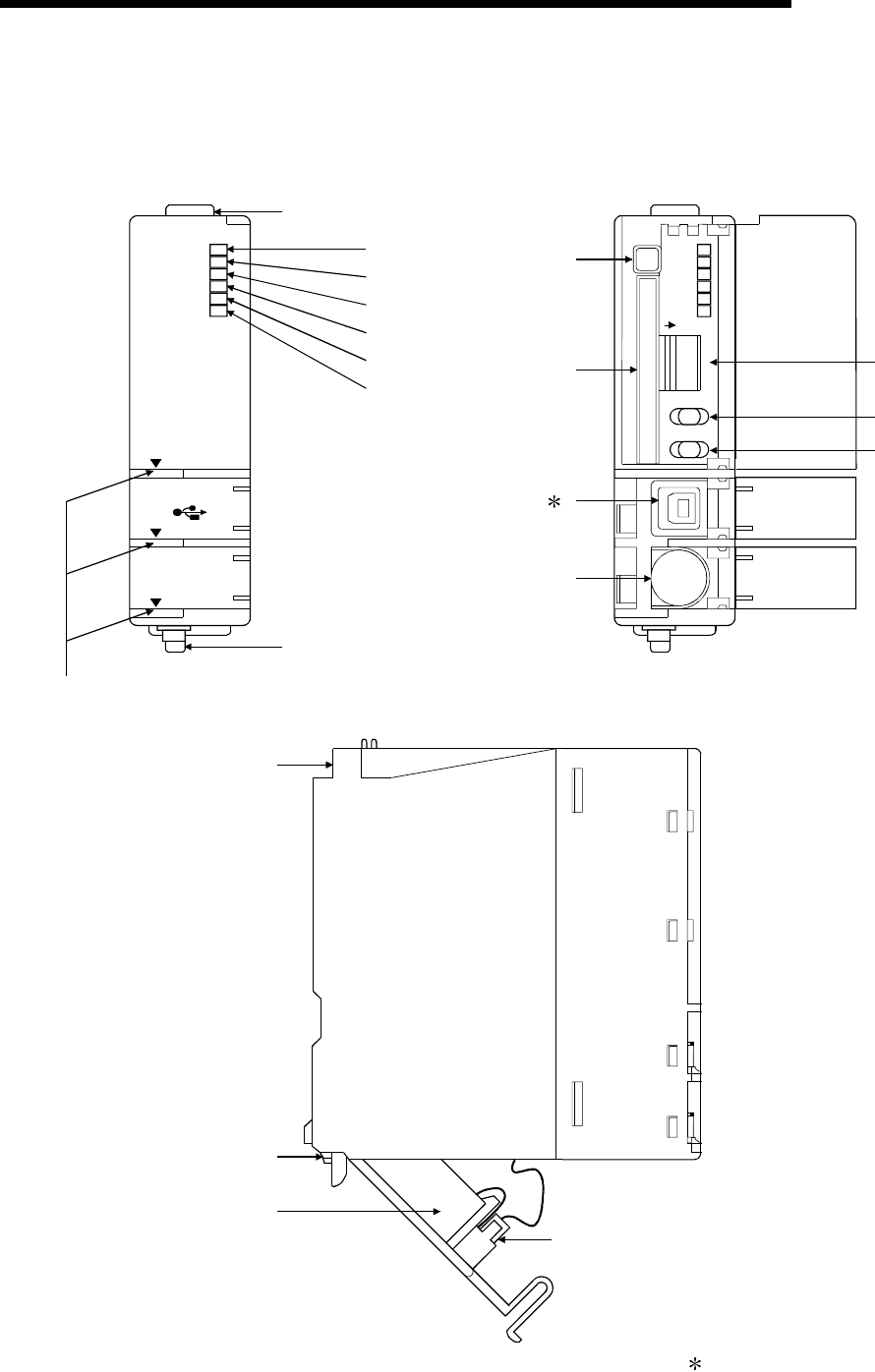
4 - 4 4 - 4
MELSEC-Q
4 HARDWARE SPECIFICATION OF THE CPU MODULE
4.2 Part Names and Settings
This section explains the part names and settings of the module.
Front face
Q02HCPU
RS-232
USB
MODE
RUN
ERR.
USER
BAT.
BOOT
1)
2)
8)
3)
4)
5)
6)
7)
PULL
W
hen opening the front cover, put your finger here.
With front cover open
MODE
RUN
ERR.
USER
BAT.
BOOT
ON SW
1
2
3
4
5
STOP RUN
RESET L CLR
9)
10)
11) 1
12)
13)
14)
15)
Side face
16)
17)
19)
18)
1: Not provided for Q02CPU.

4 - 5 4 - 5
MELSEC-Q
4 HARDWARE SPECIFICATION OF THE CPU MODULE
No. Name Application
1) Module fixing hook Hook used to fix the module to the base unit. (Single-motion installation)
2) "Mode" LED
Indicates the mode of the CPU module.
ON (green) : Q mode
ON (orange) : A mode
Flicker (green) : Enforced ON/OFF for external I/O registered
3) "RUN" LED
Indicates the operating status of the CPU module.
ON : During operation in "RUN" status.
OFF : During a stop in "STOP" status or detection of error whose occurrence stops
operation.
Flicker : When parameter/program is written at STOP and RUN/STOP switch is
changed from "STOP" to "RUN".
To turn ON the RUN LED after writing the program, carry out the following
steps.
y Set the RUN/STOP switch from "RUN" → "STOP" → "RUN".
y Reset with the RESET/L.CLR switch.
y Restart the PLC power.
To turn ON the RUN LED after writing the parameters, carry out the following
steps.
y Reset with the RESET/L.CLR switch.
y Restart the PLC power.
(If the RUN/STOP switch is set from "RUN" → "STOP" → "RUN" after
changing the parameters, the parameters related to the intelligent function
module, such as the network parameters, will not be reflected.)
4) "ERR." LED
ON : Detection of self-diagnosis error which will not stop operation, except battery
error.
(When operation continued at error detection is set in the parameter.)
OFF : Normal
Flicker : Detection of error whose occurrence stops operation.
When automatic write to standard ROM is completed normally. ("BOOT" LED
also flickers.)
5) "USER" LED
ON : Error detected by CHK instruction or annunciator ON
OFF : Normal
Flicker : Execution of latch clear
6) "BAT." LED
ON : Occurrence of battery error due to reduction in battery voltages of CPU module
or memory card.
OFF : Normal
7) "BOOT" LED
ON : Start of boot operation
OFF : Non-execution of boot operation
Flicker : When automatic write to standard ROM is completed normally. ("ERR." LED
also flickers.)
8) Module loading lever Used to load the module to the base unit.
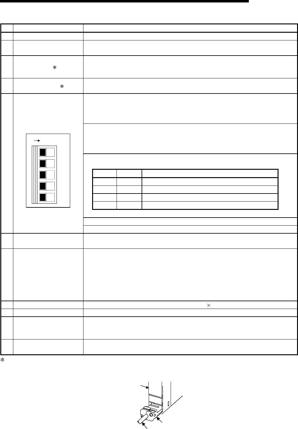
4 - 6 4 - 6
MELSEC-Q
4 HARDWARE SPECIFICATION OF THE CPU MODULE
No. Name Application
9) Memory card EJECT button Used to eject the memory card from the CPU module.
10) Memory card loading
connector Connector used to load the memory card to the CPU module.
11) USB connector 1
Connector for connection with USB-compatible peripheral device. (Connector type B)
Can be connected by USB-dedicated cable.
Not available for Q02CPU.
12) RS-232 connector 1 Connector for RS-232 connection
Can be connected by RS-232 connection cable (QC30R2).
Used to set the items for operation of the CPU module.
For system protection and parameter-valid drive functions, refer to the High
Performance model QCPU (Q mode) User's Manual (Function Explanation, Program
Fundamentals).
SW1 : Used to set system protection. Batch-inhibits write and control directives to the
CPU module. (Shipped in OFF position)
OFF : No protection
ON : Protection
SW2, SW3: Used to specify parameter-valid drive.
(Both SW2 and SW3 are shipped in OFF position)
SW2 SW3 Parameter Drive
OFF OFF Program memory (Drive 0)
ON OFF SRAM card (Drive 1)
OFF ON Flash card/ATA card (Drive 2)
ON ON Standard ROM (Drive 4)
Note: Parameters cannot be stored in standard RAM (Drive 3).
SW4 : Must not be used. Normally OFF. (Shipped in OFF position)
13)
DIP switches
1
2
3
4
5
ON SW
SW5 : Must not be used. Normally OFF. (Shipped in OFF position)
14) RUN/STOP switch RUN : Executes sequence program operation.
STOP : Stops sequence program operation.
15) RESET/L.CLR switch
RESET : Used to perform hardware reset, operation fault rest, operation initialization,
etc.
If this switch is left in the RESET position, the whole system will be reset and
the system will not operate properly.
After performing reset, always return this switch to the neutral position.
L.CLR : Used to turn "OFF" or "zero" all data in the parameter-set latch area.
Used to clear the sampling trace and status latch registration.
16) Module fixing screw hole Hole for the screw used to fix to the base unit. (M3 12 screw)
17) Module fixing latch Hook used to fix to the base unit.
18) Battery connector pin
For connection of battery lead wires.
(When shipped from the factory, the lead wires are disconnected from the connector to
prevent the battery from consuming.)
19) Battery Backup battery for use of program memory, standard RAM and power failure
compensation function.
1 : When normally connecting a cable to the USB connector or RS-232 connector, clamp the cable to prevent it from
coming off due to the dangling, moving or carelessly pulling of the cable.
Q6HLD-R2 type RS-232 Connector Disconnection Prevention Holder is available as a clamp for RS-232 connector.
Q6HLD-R2
CPU module
RS-232 cable

4 - 7 4 - 7
MELSEC-Q
4 HARDWARE SPECIFICATION OF THE CPU MODULE
4.3 Switch Operation After Writing in Program
When writing a program into the CPU module, do not turn off the system protect set
switch SW1 in advance (When the switch is turned off, the system will not be
protected).
(1) When a program is written while CPU module is stopped:
When a program is written while the CPU module is stopped, operate the switch
in the order shown below.
1) RUN / STOP switch : STOP
"RUN" LED: Turns off CPU module in stop status Write a program.
2) RESET / L.CLR switch : Tilt this switch to RESET once, and return it to the
original center position.
3) RUN / STOP switch : STOP RUN
"RUN" LED: Turns on CPU module in running status
(2) When a program is written while CPU module is running:
When a program is written while the CPU module is running, the switch need not
be operated.
POINTS
(1) Even if the RUN/STOP switch is set to RUN immediately after a program is
written when the CPU module is in the stop status, CPU module will not come
into RUN status.
When the CPU module is reset with the RESET / L.CLR switch and the
RUN/STOP switch is set to RUN after a program has been written, the CPU
module can be brought into RUN status.
(2) If the CPU module is desired to be brought into RUN status without resetting it,
operate the RUN/STOP switch from STOP to RUN, RUN to STOP, and STOP
to RUN in that order.
After the seconds STOP to RUN switch operation, the CPU module is brought
into RUN status.
(3) When a program is written while the CPU module is running in boot operation,
the program written during the running is written into the program memory.
After a program has been written while the CPU module is running, write the
program also into the boot original memory. Failure to write a program into the
boot original memory will run an old program at the time of the next boot
operation.
(For details of the boot operation, refer to the High Performance model QCPU
(Q mode) User's Manual (Function Explanation, Program Fundamentals) ).
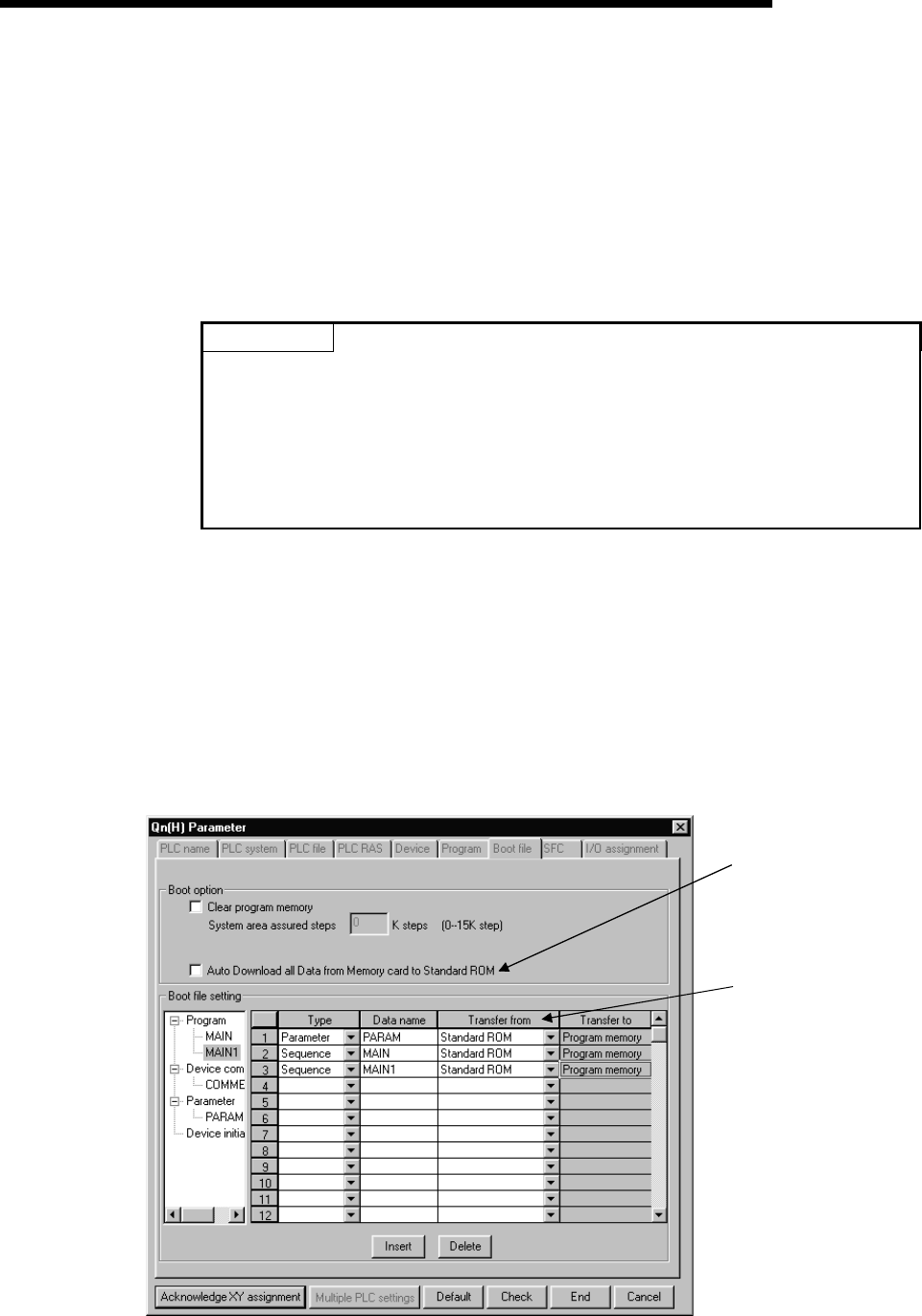
4 - 8 4 - 8
MELSEC-Q
4 HARDWARE SPECIFICATION OF THE CPU MODULE
4.4 Latch Clear Operation
To perform latch clear, operate the RESET/L.CLR switch in the following procedure.
1) RUN/STOP switch : STOP
2) RESET/L.CLR switch : Move the switch to L.CLR several times until the
USER LED flickers.
"USER" LED: Flicker Ready for latch clear.
3) RESET/L.CLR switch : Move the switch to L.CLR once more.
"USER" LED: OFF Latch clear complete.
POINTS
(1) The ineffective range for latch clear can be set for each device by the device
setting parameter.
(2) In addition to the way of using the RESET/L.CLR switch for latch clear, remote
latch clear may be performed from GX Developer.
For details of the remote latch clear operation using GX Developer, refer to the
High Performance model QCPU (Q mode) User's Manual (Function
Explanation, Program Fundamentals).
4.5 Executing Automatic Write to Standard ROM.
(1) Order of execution for automatic write to standard ROM
Automatic write to the standard ROM is carried out with the following procedures.
(a) Operation with GX Developer (setting automatic write to standard ROM)
1) Check the "Auto Download all Data from Memory card to Standard
ROM" item in the PLC parameter boot file setting.
Set the parameter and program to be booted at the "Boot file setting"
section.
(Set the "Transfer from" to "Standard ROM".)
Set the "Transfer from"
to "Standard ROM".
Check "Auto Download all
Data from Memory card to
Standard ROM ".
2) Store the set parameters and programs to be booted in the memory
card.

4 - 9 4 - 9
MELSEC-Q
4 HARDWARE SPECIFICATION OF THE CPU MODULE
(b) Operations with CPU module (automatic write to standard ROM)
1) Switch OFF the power supply to the PLC.
2) Mount the memory card that contains the parameters and programs to
be booted onto the CPU module.
3) Set the parameter's valid drive in the mounted memory card with the
CPU module's dip switches.
• When a SRAM card is mounted: SW2 : ON, SW3 : OFF
• When a Flash card/ATA card is mounted: SW2 : OFF, SW3 : ON
4) Switch on the power supply to the PLC.
5) "BOOT" LED will flicker when automatic write to standard ROM has
been completed, and the CPU module will assume a suspension error
status.
6) Switch OFF the power supply to the PLC.
7) Remove the memory card, and then set the parameter's valid drive in
the standard ROM with the CPU module's dip switches.
• Standard ROM: SW2 : ON, SW3 : ON
(c) The parameters and programs will be booted from the standard ROM to the
program memory when the PLC is switched on to enable actual operations.
5 - 1 5 - 1
MELSEC-Q
5 POWER SUPPLY MODULE
5 POWER SUPPLY MODULE
5.1 Specification
5.1.1 Power supply module specifications
This section gives the specifications of the power supply modules.
Performance Specifications
Item Q61P-A1 Q61P-A2 Q62P Q63P
Base loading position Power supply module loading slot
Applicable base unit Q3B, Q6B
100 to 120VAC +10%
-15% 200 to 240VAC +10%
-15% 100 to 240VAC +10%
-15% 24VDC +30%
-35%
Input power supply
(85 to 132VAC) (170 to 264VAC) (85 to 264VAC) (15.6 to 31.2VDC)
Input frequency 50/60Hz ±5% ——
Input voltage distortion factor Within 5% (refer to section 5.1.3) ——
Max. input apparent power 105VA ——
Max. input power —— 45W
Inrush current 20A within 8ms 100A within 1ms
5VDC 6A 3A 6A Rated output
current 24VDC —— 0.6A ——
External output voltage —— 24VDC ±10% ——
5VDC 6.6A or more 3.3A or more 6.6A or more Overcurrent
protection 1 24VDC —— 0.66A or more ——
5VDC 5.5 to 6.5V Overvoltage
protection 2 24VDC ——
Efficiency 70% or more 65% or more 70% or more
Allowable momentary power failure
period 3 Within 20ms Within 10ms
(at 24VDC input)
Dielectric withstand voltage Across inputs/LG and outputs/FG
2830VAC rms/3 cycles (2000 m (6562 ft.))
500VAC across
primary and 5VDC
Insulation resistance
Across inputs and outputs (LG and FG separated), across inputs and
LG/FG, across outputs and FG/LG 10M or more by insulation
resistance tester
10M or more by
insulation resistance
tester
Noise durability
• By noise simulator of 1500Vp-p noise voltage, 1 s noise width and 25
to 60Hz noise frequency
• Noise voltage IEC61000-4-4, 2kV
By noise simulator of
500Vp-p noise voltage,
1s noise width and
25 to 60Hz noise
frequency
Operation indication LED indication (lit at 5VDC output)
Fuse Built-in (Unchangeable by user)
Application ERR contact (contact switched off (opened: normally closed contact) at an error stop of CPU
module), for CPU module operating status output
Rated switching voltage,
current 24VDC, 0.5A
Minimum switching load 5VDC, 1mA
Response time OFF to ON: 10ms max. ON to OFF: 12ms max.
Life Mechanical : More than 2 million times
Electrical : More than 100 thousand times at rated switching voltage, current
Surge suppressor No
Contact
output
section
Fuse No
Terminal screw size M3.5 × 7
Applicable wire size 0.75 to 2mm2
Applicable solderless terminal RAV1.25 to 3.5, RAV2 to 3.5
Applicable tightening torque 66 to 89N•cm
H 98mm (3.86inch)
W 55.2mm (2.33inch)
External
dimensions D 90mm (3.55inch)
Weight 0.31kg 0.39kg 0.33kg
5
5 - 2 5 - 2
MELSEC-Q
5 POWER SUPPLY MODULE
Power Supply Module Specifications (Continued)
Performance Specifications
Item Q64P
Base loading position Power supply module loading slot
Applicable base unit Q3B, Q6B
100 to 120VAC/200 to 240VAC +10%
-15%
Input power supply
(85V to 132VAC/170 to 264VAC)
Input frequency 50/60Hz ±5%
Input voltage distortion factor Within 5% (refer to section 5.1.3)
Max. input apparent power 160VA
Inrush current 20A within 8ms
5VDC 8.5A Rated output
current 24VDC ——
5VDC 9.9A or more Overcurrent
protection*1 24VDC ——
5VDC 5.5 to 6.5V Overvoltage
protection*2 24VDC ——
Efficiency 70% or more
Allowable momentary power failure
period*3 Within 20ms
Dielectric withstand voltage Across inputs/LG and outputs/FG
2830VAC rms/3 cycles (2000 m (6562 ft.))
Insulation resistance Across inputs and outputs (LG and FG separated), across inputs and LG/FG, across outputs
and FG/LG 10M or more by insulation resistance tester
Noise durability
• By noise simulator of 1500Vp-p noise voltage, 1 s noise width and 25 to 60Hz noise
frequency
• Noise voltage IEC61000-4-4, 2kV
Operation indication LED indication (lit at 5VDC output)
Fuse Built-in (Unchangeable by user)
Application ERR contact (contact switched off (opened: normally closed contact) at an error stop of CPU
module), for CPU module operating status output
Rated switching voltage,
current 24VDC, 0.5A
Minimum switching load 5VDC, 1mA
Response time OFF to ON: 10ms max. ON to OFF: 12ms max.
Life Mechanical : More than 2 million times
Electrical : More than 100 thousand times at rated switching voltage, current
Surge suppressor No
Contact
output
section
Fuse No
Terminal screw size M3.5 × 7
Applicable wire size 0.75 to 2mm2
Applicable solderless terminal RAV1.25 to 3.5, RAV2 to 3.5
Applicable tightening torque 66 to 89N•cm
H 98mm (3.86inch)
W 55.2mm (2.33inch)
External
dimensions D 115mm (4.53inch)
Weight 0.40kg
5
5 - 3 5 - 3
MELSEC-Q
5 POWER SUPPLY MODULE
Performance Specifications
Item Q61SP
Base loading position Slim type power supply module loading slot
Applicable base unit Q3SB
100 to 240VAC +10%
-15%
Input power supply
(85 to 264VAC)
Input frequency 50/60Hz ±5%
Input voltage distortion factor Within 5% (refer to section 4.3.1)
Max. input apparent power 40VA
Inrush current 20A within 8ms
5VDC 2A Rated output
current 24VDC ——
5VDC 2.2A or more Overcurrent
protection*1 24VDC ——
5VDC 5.5 to 6.5V Overvoltage
protection*2 24VDC ——
Efficiency 70% or more
Allowable momentary power failure
period*3 Within 20ms
Dielectric withstand voltage Across inputs/LG and outputs/FG
2830VAC rms/3 cycles (2000 m (6562 ft.))
Insulation resistance Across inputs and outputs (LG and FG separated), across inputs and LG/FG, across outputs
and FG/LG 10M or more by insulation resistance tester
Noise durability
• By noise simulator of 1500Vp-p noise voltage, 1 s noise width and 25 to 60Hz noise
frequency
• Noise voltage IEC61000-4-4, 2kV
Operation indication LED indication (lit at 5VDC output)
Fuse Built-in (Unchangeable by user)
Application ERR contact (contact switched off (opened: normally closed contact) at an error stop of CPU
module), for CPU module operating status output
Rated switching voltage,
current 24VDC, 0.5A
Minimum switching load 5VDC, 1mA
Response time OFF to ON: 10ms max. ON to OFF: 12ms max.
Life Mechanical : More than 20 million times
Electrical : More than 100 thousand times at rated switching voltage, current
Surge suppressor No
Contact
output
section
Fuse No
Terminal screw size M3.5 × 7
Applicable wire size 0.75 to 2mm2
Applicable solderless terminal RAV1.25 to 3.5, RAV2 to 3.5
Applicable tightening torque 66 to 89N•cm
H 98mm (3.86inch)
W 27.4mm (1.08inch)
External
dimensions D 104mm (4.09inch)
Weight 0.18kg
5 - 4 5 - 4
MELSEC-Q
5 POWER SUPPLY MODULE
Power Supply Module Specifications (Continued)
Performance Specifications
Item A1S61PN A1S62PN A1S63P
Base loading position Power supply module loading slot
Applicable base unit QA1S65B, QA1S68B
100 to 240VAC +10%
-15% 24VDC +30%
-35%
Input power supply (85 to 264VAC) (15.6 to 31.2VDC)
Input frequency 50/60Hz ±5% ——
Input voltage distortion factor Within 5%
Max. input apparent power 105VA ——
Max. input power —— 41W
Inrush current 20A within 8ms 81A within 1ms
5VDC 5A 3A 5A Rated output
current 24VDC —— 0.6A ——
5VDC 5.5A or more 3.3A or more 5.5A or more Overcurrent
protection 1 24VDC —— 0.66A or more ——
5VDC 5.5 to 6.5V Overvoltage
protection 2 24VDC ——
Efficiency 65% or more
Allowable momentary power failure
period 3 Within 20ms Within 10ms
(at 24VDC input)
Dielectric withstand voltage Across inputs/LG and outputs/FG
2830VAC rms/3 cycles (2000 m (6562 ft.))
500VAC across primary and
5VDC
Insulation resistance
Across inputs and outputs (LG and FG separated), across inputs
and LG/FG, across outputs and FG/LG 10M or more by
insulation resistance tester
5M or more by insulation
resistance tester
Noise durability
• By noise simulator of 1500Vp-p noise voltage, 1 s noise width
and 25 to 60Hz noise frequency
• Noise voltage IEC61000-4-4, 2kV
By noise simulator of 500Vp-p
noise voltage, 1 s noise width
and 25 to 60Hz noise
frequency
Operation indication LED indication (lit at 5VDC output)
Fuse Built-in (Unchangeable by user)
Contact output section No
Terminal screw size M3.5 × 7
Applicable wire size 0.75 to 2mm2
Applicable solderless terminal RAV1.25 to 3.5, RAV2 to 3.5
Applicable tightening torque 66 to 89N•cm
H 130mm (5.12inch)
W 55mm (2.17inch)
External
dimensions D 93.6mm (3.69inch)
Weight 0.60kg 0.50kg

5 - 5 5 - 5
MELSEC-Q
5 POWER SUPPLY MODULE
POINTS
1 : Overcurrent protection
The overcurrent protection device shuts off the 5 V, 24 VDC circuit and stops
the system if the current flowing in the circuit exceeds the specified value. The
LED of the power supply module is unlit or lit dimly upon a voltage drop.
If this device is activated, switch the input power supply off and eliminate the
cause such as insufficient current capacity or short. Then, a few minutes later,
switch it on to restart the system.
The initial start for the system takes place when the current value becomes
normal.
2 : Overvoltage protection
The overvoltage protection device shuts off the 5 VDC circuit and stops the
system if a voltage of 5.5 VDC is applied to the circuit. When this device is
activated, the power supply module LED is switched OFF. If this happens,
switch the input power OFF, then a few minutes later ON. This causes the
initial start for the system to take place. The power supply module must be
changed if the system is not booted and the LED remains OFF.
3 : Allowable momentary power failure period
(1) For AC input power supply
y An instantaneous power failure lasting less than 20ms will cause AC
down to be detected, but operation will continue.
y An instantaneous power failure lasting more than 20ms may cause the
operation to continue or initial start to take place depending on the power
supply load.
Furthermore, by using the same AC power supply for the AC input
module and the power supply module, it is possible to prevent the
sensor, to which the AC input module is connected, from turning OFF
when it is ON when the power is turned OFF.
However, if only the AC input module is connected to the AC line, which
is connected to the power suppludetection of the AC down for the power
supply module may be delayed by the capacitor in the AC input module.
Thus, connect a load of approx. 30mA per QX10 unit to the AC line.
(2) For DC input power supply
y An instantaneous power failure lasting less than 10ms (*4) will cause
24VDC down to be detected, but operation will continue.
y An instantaneous power failure lasting more than 10ms (*4) may cause
the operation to continue or initial start to take place depending on the
power supply load.
(4: This is for a 24VDC input. This is 10ms or less for 24VDC or less.)
5 - 6 5 - 6
MELSEC-Q
5 POWER SUPPLY MODULE
5.1.2 Selecting the power supply module
The power supply module is selected according to the total of current consumption
of the base units, I/O modules, intelligent function module, special
function module, and peripheral devices supplied by its power supply module.
For the internal current consumption of 5 VDC of the base unit, refer to Chapter 6.
For the internal current consumption of 5 VDC of the I/O modules,
intelligent function module, special function module, and peripheral
devices, refer to the Manuals of their respective modules.
For the devices obtained by a user, see the manual for the respective device.
(1) When the base unit is of Q3B or Q6B:
Base unit
Q35B, Q65B, etc.
CPU module
Q02CPU, Q06HCPU, etc.
I/O module
QX10, QY10, etc.
Intelligent function module
Q64AD, QJ71LP21-25, etc.
1
Power supply module
Q61P-A1, Q61P-A2,
etc.
Peripheral devices, converter,
cables, etc. (for connection
between CPU module and PC)
1: The CPU module is loaded on the Q3 B main base
unit.
(a) Selection of power supply module for use of Q52B or Q55B extension base
unit
Using the Q52B or Q55B supplies 5VDC power from the power supply
module of the main base unit through the extension cable.
Therefore, note the following when using the Q52B or Q55B.
1) The power supply module to be loaded on the main base unit should be
selected to cover also the 5VDC used on the Q52B or Q55B.
For example, either of the following power supply modules must be
mounted on the main base unit, when the current consumption on the
main base unit is 3A and that on the Q52B or Q55B is 1A.
5VDC Rated output current Type
6A Q61P-A1, Q61P-A2, Q63P
8.5A Q64P
2) Since 5VDC is supplied to the Q52B or Q55B through the extension
cable, a voltage drop occurs at the extension cable.
You must select the power supply module and extension cable length to
ensure that the "IN" connector voltage of the Q52B or Q55B is 4.75VDC
or more.
For details of a voltage drop, refer to Section 6.6.
5 - 7 5 - 7
MELSEC-Q
5 POWER SUPPLY MODULE
(b) Ideas for reducing voltage drops
The following methods are effective to reduce voltage drops at the extension
cables.
1) Changing the module loading positions
Load large current consumption modules on the main base unit.
Load small current consumption modules on the extension base unit.
2) Using short extension cables
The shorter the extension cable is, the smaller the resistance and voltage
drops are.
Use the shortest possible extension cables.
(2) When the base unit is of Q3SB:
Slim type main base unit
Q32SB, Q33SB, Q35SB
CPU module
Q02(H)CPU, Q06HCPU, etc.
I/O module
QX10, QY10, etc.
Intelligent function module
Q64AD, QJ71LP21-25, etc.
1
Slim type power
supply module
Q61SP
Peripheral devices, converter,
cables, etc. (for connection
between CPU module and PC)
1: The CPU module is loaded on the Q3 SB slim type
main base unit.
(a) To use the slim type main base unit and slim type power supply module, pay
attention to the capacity of the 5VDC power supply.
1) The capacity of the 5VDC power supply of the power supply module
(Q61SP) installed to the slim type main base unit is 2A. Choose modules
with total capacity of 2A or less.
5VDC Rated output current Type
2.0A Q61SP
5 - 8 5 - 8
MELSEC-Q
5 POWER SUPPLY MODULE
(3) When the base unit is of QA1S6B:
Base unit
QA1S65B and QA1S68B
I/O module
A1SX10, A1SY10, etc.
Special function module
A1SD61, A1SD75P1-S3, etc.
peripheral devices
AD75TU 2
Power supply module
A1S61PN, A1S62PN,
A1S63P
2: Select the power supply module also in
consideration of the current consumption of the
peripheral devices connected to the special
function module.
For example, when the AD75TU is connected
to the A1SD75P1-S3, the current consumption
of the AD75TU must also be taken into
account.
5.1.3 Precaution when connecting the uninterruptive power supply
Be sure of the following terms when connecting the High Performance model QCPU
system to the uninterruptive power supply (abbreviated as UPS hereafter):
Use a UPS which employs the constant inverter power supply method with 5 % or less
voltage fluctuation.
Do not use a UPS with the constant commercial power supply method.
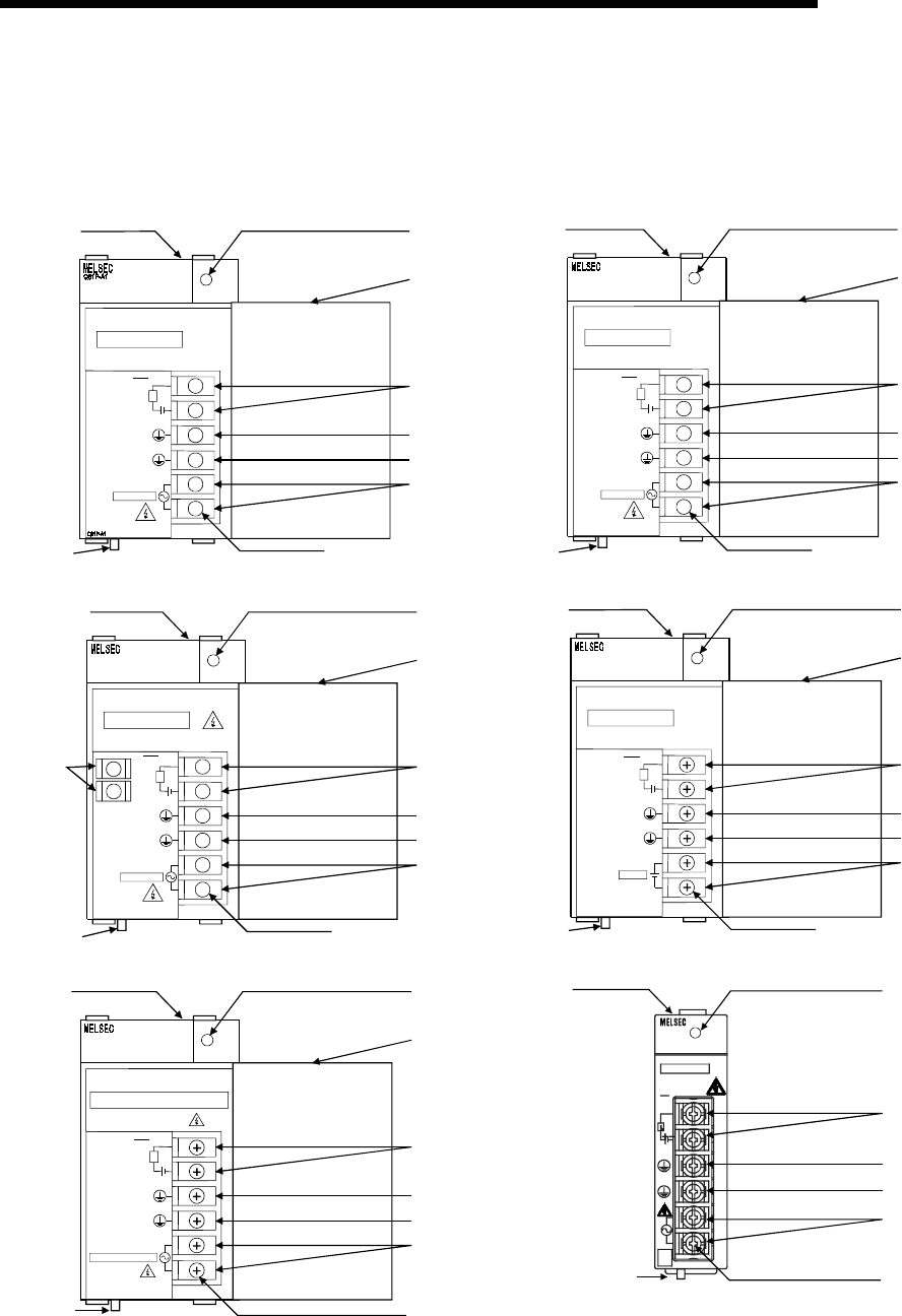
5 - 9 5 - 9
MELSEC-Q
5 POWER SUPPLY MODULE
5.2 Names of Parts and Settings
The names of the parts of each power supply module are described below.
(1) Q61P-A1, Q61P-A2, Q62P, Q63P, Q64P, Q61SP
POWER
100-120VAC
INPUT
50/60Hz 105VA
OUTPUT 5VDC 6A
ERR.
L
+-
24VDC 0.5A
(FG)
(LG)
N
L
100-120VAC
INPUT
8) 1)
7)
2)
3)
4)
10
)
9) 6)
Q61P-A1
+
+
+
+
+
+
POWER
200-240VAC
INPUT
50/60Hz 105VA
OUTPUT 5VDC 6A
ERR.
L
+-
24VDC 0.5A
(FG)
(LG)
N
L
200-240VAC
INPUT
8) 1)
7)
2)
3)
4)
11)
9)
Q61P-A2
Q61P-A2
6)
Q61P-A2
+
+
+
+
+
+
POWER
100-240VAC
INPUT
50/60Hz 105VA
OUTPUT 5VDC 3A 24VDC 0.6A
ERR.
L
+-
24VDC 0.5A
(FG)
(LG)
N
L
100-240VAC
INPUT
8) 1)
7)
2)
3)
4)
12)
9) 6)
Q62P
Q62P
Q62P
+24V
24G
5) +
+
+
+
+
+
+
+
Q63P
POWER
24VDC
INPUT
MAX 45W
OUTPUT 5VDC 6A
ERR.
L
+-
24VDC 0.5A
(FG)
(LG)
+24V
24VDC
INPUT
12) 1)
7)
2)
3)
4)
13)
9) 6)
Q63P
24G
Q63P
Q64P
POWER
100-120/200-240VAC
INPUT
50/60Hz 160VA
OUTPUT 5VDC 8.5A
ERR.
L
+-
24VDC 0.5A
(FG)
(LG)
N
L
100-120/200-240VAC
INPUT
8) 1)
7)
2)
3)
4)
14)
9)
Q64P
Q64P
6)
Q61SP
100-
240V
AC
Q61SP
POWER
INPUT
50/60Hz 40VA
100-240VAC
ERR.
24VDC
0.5A
INPUT
OUTPUT 5VDC 2A
MITSUBISHI
8) 1)
2)
3)
4)
12)
6)
9)
(FG)
(LG)
N
L
Q61SP
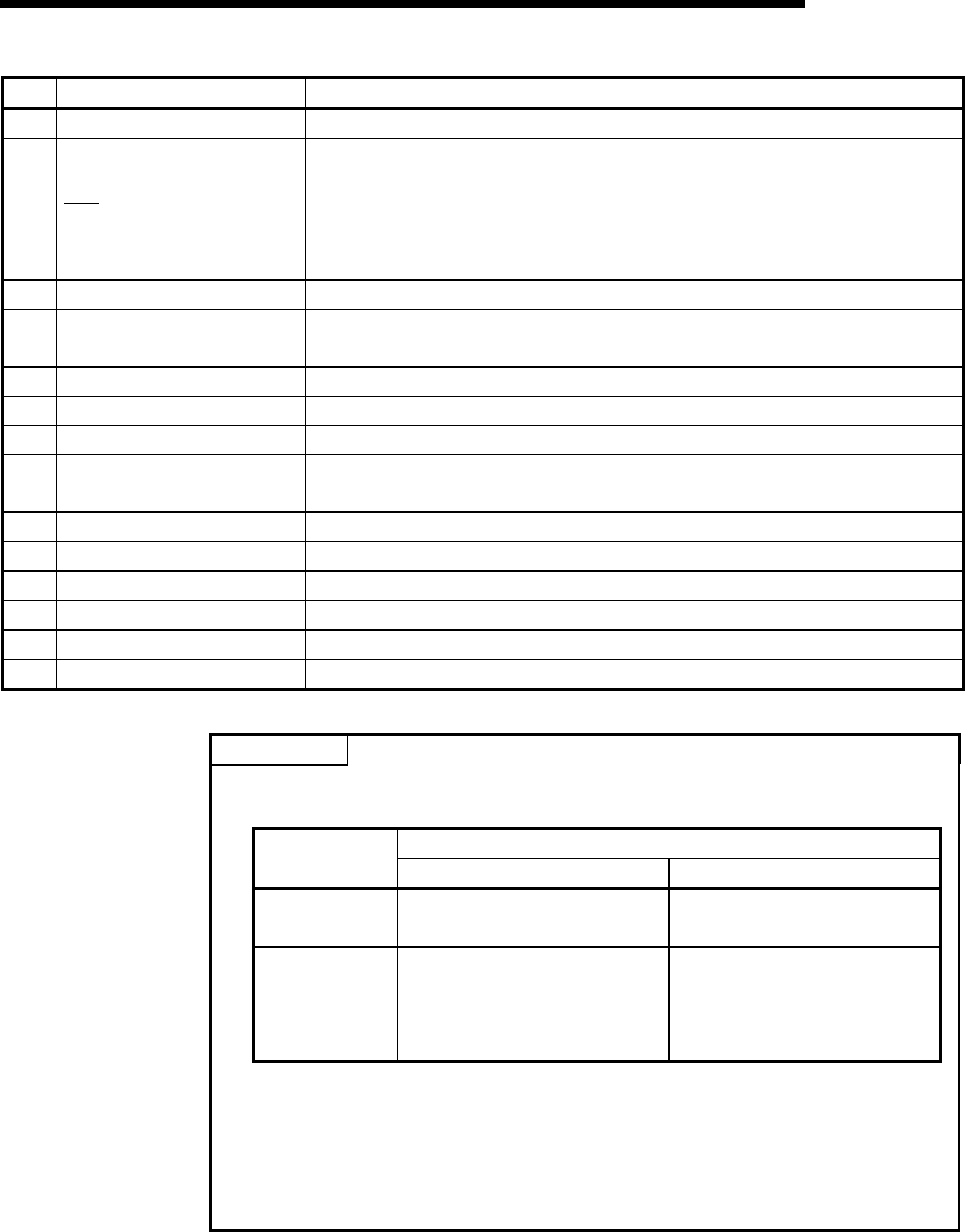
5 - 10 5 - 10
MELSEC-Q
5 POWER SUPPLY MODULE
No. Name Application
1) POWER LED 5VDC power indicator LED
2) ERR terminals
1) Turned ON when the whole system operates normally.
2) Turned OFF (opened) when a stop error occurs in the CPU module.
3) In a multiple CPU system configuration, turned OFF when a stop error occurs in
any of the CPU modules.
Normally off when loaded in an extension base unit.
3) FG terminal Ground terminal connected to the shield pattern of the printed circuit board.
4) LG terminal Grounding for the power supply filter. The potential of Q61P-A1, Q61P-A2, Q62P,
Q64P and Q61SP terminal is 1/2 of the input voltage
5) +24V, 24G terminals Used to supply 24VDC power to inside the output module (using external wiring).
6) Terminal screw M3.5 × 7 screw
7) Terminal cover Protective cover of the terminal block
8) Module fixing screw hole Used to fix the module to the base unit. M3 × 12 screw (user-prepared)
(Tightening torque : 36 to 48N•cm)
9) Module loading lever Used to load the module into the base unit.
10) Power input terminals Used to connect a 100VAC power supply.
11) Power input terminals Used to connect a 200VAC power supply.
12) Power input terminals Used to connect a 100VAC to 200VAC power supply.
13) Power input terminals Used to connect a 24VAC power supply.
14) Power input terminals Used to connect a 100VAC/200VAC power supply.
POINTS
(1) The Q61P-A1 is dedicated for inputting a voltage of 100 VAC.
Do not input a voltage of 200 VAC into it or trouble may occur on the Q61P-A1.
Supply power voltage Power
module type 100VAC 200VAC
Q61P-A1 Operates normally. Power supply module
causes trouble.
Q61P-A2
Power supply module does
not cause trouble.
CPU module cannot be
operated.
Operates normally.
(2) Q64P automatically switches the input range 100/200VAC.
Therefore, it is not compatible with the intermediate voltage (133 to 169VAC).
The CPU module may not work normally if the above intermediate voltage is
applied.
(3) Ensure that the earth terminals LG and FG are grounded.
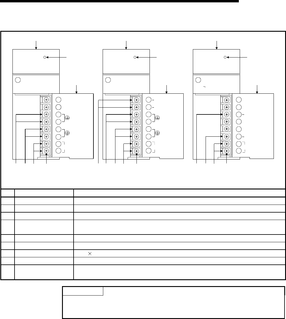
5 - 11 5 - 11
MELSEC-Q
5 POWER SUPPLY MODULE
(2) A1S61PN, A1S62PN and A1S63P
MELSECA1S61PN
POWER
MITSUBISHI
INPUT
100-240VAC
105VA
50 / 60Hz
OUTPUT
5VDC 5A
INPUT
100-240VAC
(FG)
(LG)
A1S61PN
NC
NC
8)
1)
9)
3) 4) 5) 7)
A1S61PN
MELSECA1S62PN
POWER
MITSUBISHI
INPUT
100-240VAC
105VA
50 / 60Hz
OUTPUT
5VDC 3A
24VDC 0.6A
+24V
24G
INPUT
100-240VAC
(FG)
(LG)
A1S62PN
8)
1)
9)
3) 4) 5) 7)
2)
A1S62PN
MELSECA1S63P
POWER
MITSUBISHI
INPUT
DC15.6 31.2V OUTPUT
DC 5V 5A
FG
LG
INPUT
+24V
24G
NC
NC
NC
NC
8)
1)
9)
3) 4) 6) 7)
A1S63P
No. Name Application
1) POWER LED 5VDC power indicator LED
2) +24V, 24G terminals Used to supply 24VDC power to inside the output module (using external wiring).
3) FG terminals Ground terminal connected to the shield pattern of the printed circuit board.
4) LG terminals Grounding for the power supply filter. The potential of A1S61PN or A1S62PN terminal is
1/2 of the input voltage.
5) Power input terminals Used to connect a 100VAC to 200VAC power supply.
6) Power input terminals Used to connect a 24 VDC power supply.
7) Terminal screw M3.5 7 screw
8) Terminal cover Protective cover of the terminal block
9) Module fixing screw Used to fix the module to the base unit.
(M4 screw, tightening torque : 66 to 89N•cm)
POINTS
(1) Do not wire to those terminals for which NC is stamped on the terminal block.
(2) Ensure that the earth terminals LG and FG are grounded.
6 - 1 6 - 1
MELSEC-Q
6 BASE UNIT AND EXTENSION CABLE
6 BASE UNIT AND EXTENSION CABLE
This section describes the specifications of the extension cables for the
base units (main, slim type and extension base unit) used in the PLC
system and the specification standards of the extension base unit.
6.1 Base Unit Specification Table
(1) Main base unit specifications
Type
Item Q33B Q35B Q38B Q312B
Number of I/O modules
installed 3 5 8 12
Possibility of extension Extendable
Applicable module Q series modules
5 VDC internal current
consumption 0.105A 0.110A 0.114A 0.121A
Mounting hole size M4 screw hole or 4.5 hole (for M4 screw)
H 98mm (3.86inch)
W 189mm (7.44inch) 245mm (9.65inch) 328mm (12.92inch)
439mm (17.30inch)
External
dimensions
D 44.1mm (1.74inch)
Weight 0.21kg 0.25 kg 0.35 kg 0.45 kg
Attachment Mounting screw M4 14 4 pieces (DIN rail mounting adapter to be sold separately)
DIN rail mounting
Adapter type Q6DIN3 Q6DIN2 Q6DIN1
(2) Slim type main base unit specifications
Type
Item Q32SB Q33SB Q35SB
Number of I/O modules
installed 2 3 5
Possibility of extension Cannot connect extension modules.
Applicable module Q series modules
5 VDC internal current
consumption 0.086A 0.086A 0.091A
Mounting hole size M4 screw hole or 4.5 hole (for M4 screw)
H 98mm (3.86inch)
W 114mm (4.49inch) 142mm (5.59inch) 198mm (7.80inch)
External
dimensions
D 18.5mm (0.73inch)
Weight 0.12kg 0.15 kg 0.21 kg
Attachment Mounting screw M4 12 4 pieces (DIN rail mounting adapter to be sold separately)
DIN rail mounting
Adapter type Q6DIN3
6
6 - 2 6 - 2
MELSEC-Q
6 BASE UNIT AND EXTENSION CABLE
(3) Extension base unit specifications (Type not requiring power supply
module)
Type
Item Q52B Q55B
Number of I/O modules
installed 2 5
Possibility of extension Extendable
Applicable module Q series modules
5 VDC internal current
consumption 0.080A 0.100A
Mounting hole size M4 screw hole or 4.5 hole (for M4 screw)
H 98mm (3.86inch)
W 106mm (4.17inch) 189mm (7.44inch)
External
dimensions D 44.1mm (1.74inch)
Weight 0.14kg 0.23kg
Attachment Mounting screw M4 14 4 pieces (DIN rail mounting adapter to be sold separately)
DIN rail mounting
Adapter type Q6DIN3
(4) Extension base unit specifications (Power supply loaded type)
Type
Item Q63B Q65B Q68B Q612B QA1S65B QA1S68B
Number of I/O
modules installed 3 5 8 12 5 8
Possibility of
extension Extendable
Applicable module Q series modules AnS series modules
5 VDC internal current
consumption 0.105A 0.110A 0.114A 0.121A 0.117A 0.118A
Mounting hole size M4 screw hole or 4.5 hole
(for M4 screw)
M5 screw hole or 5.5 hole
(for M5 screw)
H
98mm (3.86inch) 130mm (5.12inch)
W
189mm
(7.44inch)
245mm
(9.65inch)
328mm
(12.92inch)
439mm
(17.30inch)
315mm
(12.41inch)
420mm
(16.55inch)
External
dimensions
D
44.1mm (1.74inch) 51.2mm (2.02inch)
Weight 0.23kg 0.25 kg 0.35 kg 0.45 kg 0.75 kg 1.00 kg
Attachment Mounting screw M4 14 , 4 pieces
(DIN rail mounting adapter sold separately)
Mounting screw M5 25
4 pieces
DIN rail mounting
Adapter type Q6DIN3 Q6DIN2 Q6DIN1 ——— ———
6
6 - 3 6 - 3
MELSEC-Q
6 BASE UNIT AND EXTENSION CABLE
6.2 Extension Cable Specification Table
The list below shows the specifications of the extension cables which can
be used for the High Performance model QCPU system.
Type
Item QC05B QC06B QC12B QC30B QC50B QC100B
Cable length 0.45m (1.48ft.) 0.6m (1.97ft.) 1.2m (3.93ft.) 3.0m (9.84ft.) 5.0m (16.39ft.) 10.0m (32.79ft.)
Application Connection across the main base unit and extension base unit or across the extension base units.
Weight 0.15 kg 0.16 kg 0.22 kg 0.40 kg 0.60 kg 1.11 kg
POINT
When the extension cables are used in combination, limit the overall distance
of the combined cable to 13.2 m(43.28 ft.).
6.3 Parts Names of Base Unit
The names of the parts of the base unit are described below.
(1) Main base unit(Q33B, Q35B, Q38B, Q312B)
1)
2)
5) 4)
3) 6)
I/11I/10I/09I/08I/07I/06I/05I/04I/03I/02I/01I/00
CPU
POWER
5V
56
F6
No. Name Application
1) Extension cable
connector
Connector for sending and receiving signals from the extension base unit, to which the
extension cables are connected.
2) Base cover
Protective cover of extension cable connector. Before an extension cable is connected,
the area of the base cover surrounded by the groove under the word "OUT" on the base
cover must be removed with a tool such as nippers.
3) Module connector
Connector for installing the power supply module, CPU module, I/O modules, and
intelligent function module.
To the connectors located in the spare space where these modules are not installed, attach
the supplied connector cover or the blank cover module (QG60) to prevent entry of dirt.
4) Module fixing screw hole Screw hole for fixing the module to the base unit. Screw size:M3 12
5) Base mounting hole Hole for mounting this base unit onto the panel of the control panel (for M4 screw)
6) DIN rail adapter
mounting hole Hole for mounting DIN rail adapter
6 - 4 6 - 4
MELSEC-Q
6 BASE UNIT AND EXTENSION CABLE
(2) Slim type main base unit(Q32SB, Q33SB, Q35SB)
SG
5V
I/O3I/O2 I/O4I/O0 I/O1
CPU
POWER
5V
56
1)
2)
3)
4)
No. Name Application
1) Module connector
Connector for installing the power supply module, CPU module, I/O modules, and
intelligent function module.
To the connectors located in the spare space where these modules are not installed, attach
the supplied connector cover or the blank cover module (QG60) to prevent entry of dirt.
2) Module fixing screw hole Screw hole for fixing the module to the base unit. Screw size:M3 12
3) Base mounting hole Hole for mounting this base unit onto the panel of the control panel (for M4 screw)
4) DIN rail adapter
mounting hole Hole for mounting DIN rail adapter
6 - 5 6 - 5
MELSEC-Q
6 BASE UNIT AND EXTENSION CABLE
(3) Extension base unit (Q5 B, Q6 B, QA1S6 B)
Q52B, Q55B
I/O2I/O1I/O0 I/O3 I/O4
OUTIN
6)
3)
2)
1)
7) 4)
5)
Q63B,Q65B, Q68B, Q612B
6)
3)
5)
2)
4) 7)
I/11I/10I/09I/08I/07I/06I/05I/04I/03I/02I/01I/00
POWER
5V
56
1)
OUTIN
QA1S65B, QA1S68B
I/O0 I/O7I/O6I/O5I/O4I/O3I/O2I/O1
QA1S68B
6)
3)
2)
1)
5)
4)
POWER
5V
SG
FG
IN OUT
No. Name Application
1) Extension cable
connector
Connectors for sending and receiving signals from the main base unit or the other
extension base units, to which the extension cables are connected.
Do not remove the supplied connector cover.
2) Base cover Protective cover of extension cable connector.
3) Stage No. setting
connector Connector for setting the number of stages of the extension base unit.
For setting method, refer to Section 6.4.
4) Module connector
Connectors for installing the power supply module, I/O modules, and intelligent function
module/ special function module.
To those connectors located in the spare space where these modules are not installed,
apply the supplied connector cover or the blank cover module to prevent entry of dirt.
Blank cover module applicable to Q52B, Q55B, Q63B,Q65B, Q68B and Q612B :QG60
Blank cover module applicable to QA1S65B and QA1S68B :A1SG60
5) Module fixing screw hole Screw hole for fixing the module to the base unit.
Q52B, Q55B, Q63B,Q65B,Q68B and Q612B.............Screw size: M3 12
QA1S65B and QA1S68B.............................................Screw size: M4 12
6) Base mounting hole Hole for mounting this base unit on the panel of the control panel.
Q52B, Q55B, Q65B,Q68B and Q612B ..........For M4 screw
QA1S65B and QA1S68B................................For M5 screw
7) DIN rail adapter
mounting hole DIN rail adapter mounting hole.
6 - 6 6 - 6
MELSEC-Q
6 BASE UNIT AND EXTENSION CABLE
6.4 Setting the Extension Base Unit
The number of stages setting method of each extension base unit to be used when
extension base units are installed is described below.
IN
1
2
3
4
5
6
7
PIN1
OUT
Stage No.
setting connector
Setting of Stage Number for Extension Base Units
Number Setting for Extension Stages
1st stage 2nd stage 3rd stage 4th stage 5th stage 6th stage 7th stage
Setting of stage
No. setting
connector
POINTS
To set the stages No. setting connector, set a number from 1 to 7 according to the
number of extension stages.
Do not set the same stage number at two or more positions or do not fail to set a
number. A miss-input or miss-output may occur.
6 - 7 6 - 7
MELSEC-Q
6 BASE UNIT AND EXTENSION CABLE
6.5 I/O Number Allocation
The I/O numbers are automatically allocated in the system loading status.
O
U
T
X/Y
0
X/Y
20
X/Y
40
X/Y
60
X/Y
80
X/Y
C0
X/Y
E0
X/Y
100
X/Y
120
X/Y
140
X/Y
160
X/Y
180
01234
6 7 8 9 10 11 125
X/Y
A0
X/Y
1C0
X/Y
1E0
X/Y
200
X/Y
220
X/Y
240
X/Y
260
X/Y
280
14 15 16 17 18 19 2013
X/Y
1A0
X/Y
2C0
X/Y
2E0
X/Y
300
X/Y
320
22 23 24 2521
X/Y
2A0
1st
extension
stage
I
N
O
U
T
Power supply
module
CPU
module
Power supply
module
Power supply
module
Power supply
module
I
N
O
U
T
I
N
O
U
T
2nd
extension
stage
3rd
extension
stage
In this system, 32-point modules are loaded on slots 0 to 25.
For the I/O number setting method using GX Developer, refer to the Operating Manual
of GX Developer.
For details of I/O number allocation, refer to the following manual.
• High Performance Model QCPU (Q mode) User's Manual (Function Explanation,
Program Fundamentals)
POINT
For the extension using the Q5 B, Q6B B and QA1S6 B, allocate the I/O
numbers on the modules starting from the Q series module installed on the Q5 B,
Q6 B base unit.
<Example> Where 32 modules are installed in all slots with the configuration
shown below.
Q38B main base unit
Q68B extension base unit
QA1S68B extension base unit
QA1S68B extension base unit
00 to FF
100 to 1FF
200 to 2FF
300 to 3FF
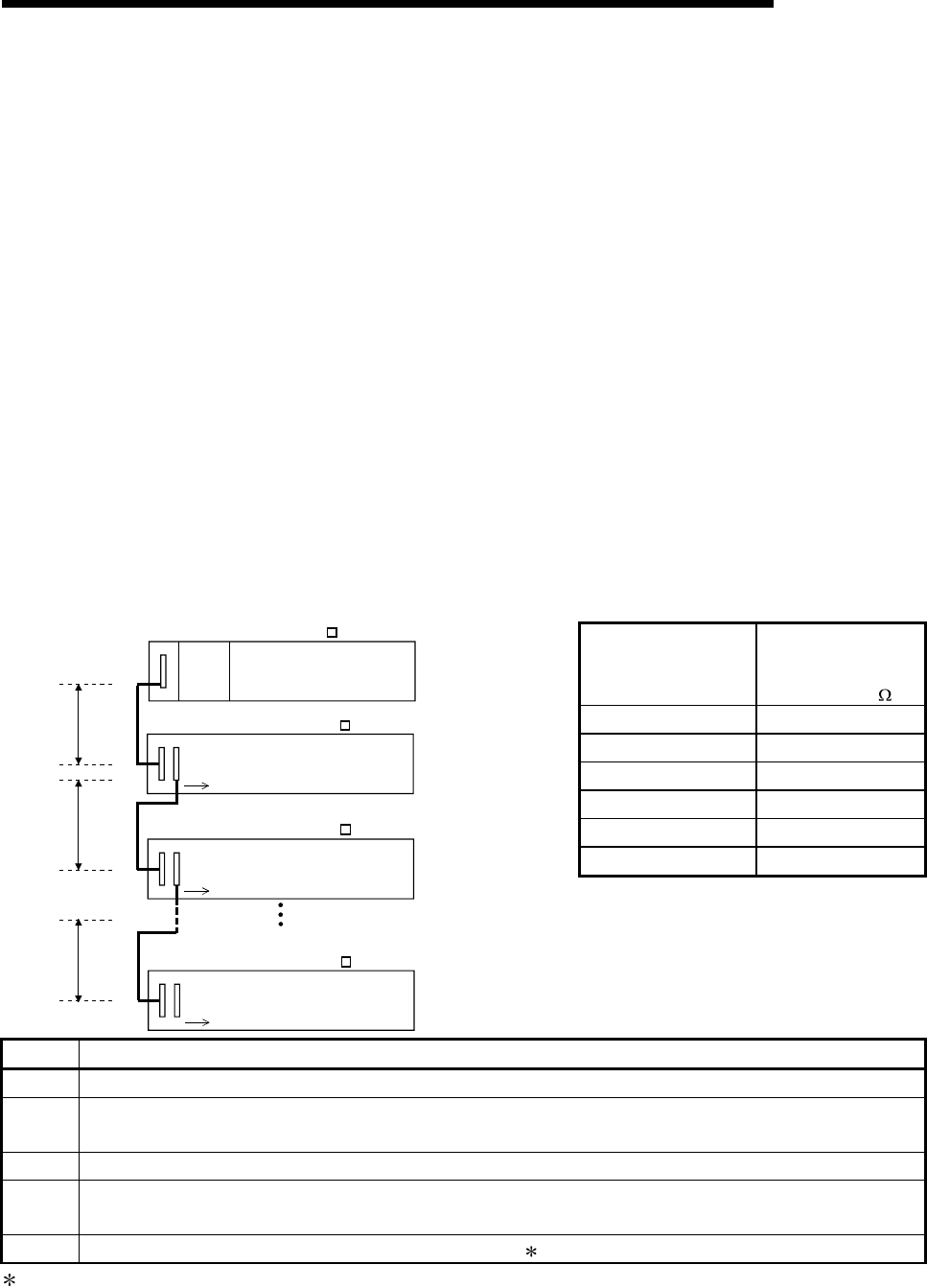
6 - 8 6 - 8
MELSEC-Q
6 BASE UNIT AND EXTENSION CABLE
6.6 Guideline for Use of Extension Base Units (Q5B)
Since the Q5B is supplied with 5VDC from the power supply module on the main
base unit, a voltage drop occurs at extension cables.
Improper I/O may be provided if the specified voltage (4.75VDC or higher) is not
supplied to the "IN" connector of the Q5B.
When using the Q5B, make sure that the "IN" connector of the Q5B is supplied
with 4.75VDC or higher.
And it is recommend to connect it with the shortest possible extension cable right after
connecting the main base unit, so as to minimize the effects of voltage drop.
(1) When only the Q5B is connected to the extension base unit
(a) Selection condition
4.75VDC or higher should be supplied to the "IN" connector of the Q5B in
the final extension stage.
(b) How to calculate voltage to "IN" connector
The 5VDC output voltage of the power supply module on the main base
unit is set to at least 4.90VDC.
Therefore, the Q5B can be used if the voltage drop is 0.15VDC or lower
(4.9VDC - 4.75VDC = 0.15VDC).
Extension Cable
Type
Extension Cable
Conductor
Resistance ( )
QC05B 0.044
QC06B 0.051
QC12B 0.082
QC30B 0.172
QC50B 0.273
QC100B 0.530
V1
V2
R7
R1
R2
R7
Power
supply
module
Extension stage 1
Extension stage 2
Extension stage 7
Main base unit (Q3 B)
Extension base unit (Q5 B)
Extension base unit (Q5 B)
Extension base unit (Q5 B)
l1
l2
l7
Symbol Description
V1 Voltage drop at the extension cable between the main base unit and extension base unit
Vn Voltage drop at the extension cable between the extension base unit (extension stage n-1) and extension base
unit (extension stage n)
R1 Cable resistance between the main base unit and extension base unit
Rn Cable resistance between the extension base unit (extension stage n-1) and extension base unit (extension
stage n)
l1 to l7 5VDC current consumption among extension stage 1 to 7 1
1: Sum total of current consumed by Q5B and currents consumed by the I/O, intelligent function modules loaded on the
Q5B.
The symbols including "I" (I1 to I7) vary with the modules loaded on the extension base unit. For details of the symbol,
refer to the user's manuals of the module used.
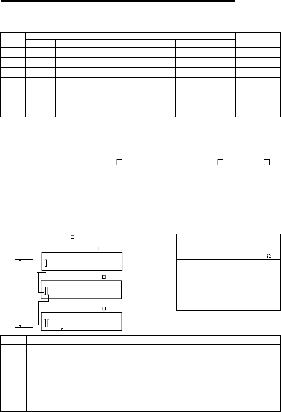
6 - 9 6 - 9
MELSEC-Q
6 BASE UNIT AND EXTENSION CABLE
List for Calculating Voltage Drops Occurring at Extension Cables in System Consisting of Extensions 1 to 7
Voltage Drop at Extension Cable on Corresponding Extension Unit
Q5B
Loading
Position V1 V2 V3 V4 V5 V6 V7
Sum Total of Voltage
Drops to "IN" Connector
of Q5B (V)
Extension
stage 1 R1 • I1 ---- ---- ---- ---- ---- ---- V=V1
Extension
stage 2 R1(I1+I2) R2 • I2 ---- ---- ---- ---- ---- V=V1+V2
Extension
stage 3 R1(I1+I2+I3) R2(I2+I3) R3 • I3 ---- ---- ---- ---- V=V1+V2+V3
Extension
stage 4 R1(I1+I2+I3+I4) R2(I2+I3+I4) R3(I3+I4) R4 • I4 ---- ---- ---- V=V1+V2+V3+V4
Extension
stage 5 R1(I1+I2+I3+I4
+I5) R2(I2+I3+I4+I5) R3(I3+I4+I5) R4(I4+I5) R5 • I5 ---- ---- V=V1+V2+V3+V4+V5
Extension
stage 6 R1(I1+I2+I3+I4
+I5+I6) R2(I2+I3+I4+I5
+I6) R3(I3+I4+I5+I6) R4(I4+I5+I6) R5(I5+I6) R6 • I6 ---- V=V1+V2+V3+V4+V5+
V6
Extension
stage 7 R1(I1+I2+I3+I4
+I5+I6+I7) R2(I2+I3+I4+I5
+I6+I7) R3(I3+I4+I5+I6
+I7) R4(I4+I5+I6+I7) R5(I5+I6+I7) R6(I6+I7) R7 • I7 V=V1+V2+V3+V4+V5+
V6+V7
The voltage supplied to "IN" connector of the Q5B in the final extension reaches 4.75
VDC or higher on the condition that the sum total of voltage drop to "IN" connector of
Q5B (V) is 0.15V or lower.
(2) When the Q6 B is connected between the Q3 B and the Q5 B
(a) Selection condition
4.75VDC or higher should be supplied to the "IN" connector of the Q5B in
the final extension.
(b) How to calculate voltage to "IN" connector
The 5VDC output voltage of the power supply module on the main base
unit is set to at least 4.90VDC.
Therefore, the Q5B can be used if the voltage drop is 0.15VDC or lower
(4.9VDC - 4.75VDC = 0.15VDC).
Extension Cable
Type
Extension Cable
Conductor
Resistance ( )
QC05B 0.044
QC06B 0.051
QC12B 0.082
QC30B 0.172
QC50B 0.273
QC100B 0.530
[When the Q5 B is connected to Extension stage 2.]
V
R1
I1
Main base unit (Q3 B)
Extension stage 1
Extension stage 2
Power
supply
module
Extension base unit (Q6 B)
Extension base unit (Q5 B)
Power
supply
module
Symbol Description
V Voltage drop at the extension cable between the main base unit and extension base unit (Q5B)
In
5VDC current consumption when the Q5B is used as Extension n+1, n = 1 to 6, n: Extension No. of Q6B
connected
(Sum total of current consumed by Q5B and currents consumed by the I/O, intelligent function modules
loaded on the Q5B.)
Rn Extension cable resistance between the main base unit or the extension base unit (Q6B) and the extension
base unit (Q6B)
Rn+1 Extension cable resistance between the extension base unit (Q6B) and extension base unit (Q5B)
6 - 10 6 - 10
MELSEC-Q
6 BASE UNIT AND EXTENSION CABLE
List for Calculating Voltage Drops Occurring at Extension Cables when connecting
Q6B between Q3B and Q5B
Position of extension base unit
Q6B Q5B
Voltage drop caused by extension
cable from the main base unit to the
Q5B IN connector (V)
Extension stage 1 Extension stage 2 V=(R1+R2)I1
Extension stage 1,
Extension stage 2 Extension stage 3 V=(R1+R2+R3)I1
Extension stage 1 to 3 Extension stage 4 V=(R1+R2+R3+R4)I1
Extension stage 1 to 4 Extension stage 5 V=(R1+R2+R3+R4+R5)I1
Extension stage 1 to 5 Extension stage 6 V=(R1+R2+R3+R4+R5+R6)I1
Extension stage 1 to 6 Extension stage 7 V=(R1+R2+R3+R4+R5+R6+R7)I1
The voltage supplied to the "IN" connector of the Q5B reaches 4.75 VDC or
higher on the condition that the voltage drop (V) at the extension cable between
the main base unit and Q5B is 0.15 VDC or lower.
(3) When the GOT is bus-connected
(a) Selection condition
4.75VDC or higher should be supplied to the "IN" connector of the Q5B.
(b) How to calculate voltage to "IN" connector
The 5VDC output voltage of the power supply module on the main base
unit is set to at least 4.90VDC.
Therefore, the Q5B can be used if the voltage drop is 0.15VDC or lower
(4.9VDC - 4.75VDC = 0.15VDC).
Extension Cable
Type
Extension Cable
Conductor
Resistance ( )
QC05B 0.044
QC06B 0.051
QC12B 0.082
QC30B 0.172
QC50B 0.273
QC100B 0.530
R1
I1
GOT
GOT
I2
Power
supply
module
Extension base unit (Q5 B)
Number of GOTs connect ed : Max. 5 unit
s
Main base unit (Q3 B)
Symbol Description
V Voltage drop at the extension cable between the main base unit and extension base unit (Q5B)
In
5VDC current consumption when the Q5B is used as Extension n+1, n = 1 to 5, n: Extension No. of the
Q6B connected
(Sum total of current consumed by Q5B and currents consumed by I/O, intelligent function modules loaded
on the Q5B)
Im 5VDC current consumption of the GOT (current consumption per GOT is 254mA)
• Im = 254 c (c: Number of GOTs connected (c: 1 to 5))
Rn Extension cable resistance between the main base unit or the extension base unit (Q6B) and extension
base unit (Q6B)
Rn+1 Extension cable resistance between the extension base unit (Q6B) and extension base unit (Q5B)

6 - 11 6 - 11
MELSEC-Q
6 BASE UNIT AND EXTENSION CABLE
POINT
When connecting GOT by extension cable that is 13.2 m (43.31ft) or longer, the
bus extension connector box A9GT-QCNB is required.
Since the A9GT-QCNB is supplied with 5VDC from the power supply module
loaded on the main base unit, 29mA must be added to "Im" as the current
consumption of the A9GT-QCNB.
For details of the GOT-bus connection, refer to the GOT-A900 Series User's
Manual (Connection).
7 - 1 7 - 1
MELSEC-Q
7 MEMORY CARD AND BATTERY
7 MEMORY CARD AND BATTERY
This section describes the specifications and handling of the memory card and battery
which can be used on the High Performance model QCPU.
The memory card is necessary for sampling tracing.
The memory card is also used to handle file registers of more than the number of
points that can be stored in the standard RAM. (Refer to Section 4.1)
7.1 Memory Card Specifications
The specifications of the memory card which can be used on the High Performance
model QCPU adheres to the PCMCIA small PC card.
On the High Performance model QCPU, only one memory card can be installed.
(1) SRAM card
Type
Item Q2MEM-1MBS Q2MEM-2MBS
Memory capacity after format 1011.5 kbyte 2034 kbyte
Storable number of files 256 288
Number of insertions and extractions 5000 times
H 45mm (1.77inch)
W 42.8mm (1.69inch)
External dimensions
D 3.3mm (0.13inch)
Weight 15g
(2) Flash card
Type
Item Q2MEM-2MBF Q2MEM-4MBF
Memory capacity after format 2035 kbyte 4079 kbyte
Storable number of files 288
Number of insertions and extractions 5000 times
Number of writings 100000 times
H 45mm (1.77inch)
W 42.8mm (1.69inch)
External dimensions
D 3.3mm (0.13inch)
Weight 15g
(3) ATA card
Type
Item Q2MEM-8MBA Q2MEM-16MBA Q2MEM-32MBA
Memory capacity after format 7940 kbyte 15932 kbyte 31854 kbyte
Storable number of files 512
Number of insertions and extractions 5000 times
Number of writings 1000000 times
H 45mm (1.77inch)
W 42.8mm (1.69inch)
External dimensions
D 3.3mm (0.13inch)
Weight 15g
7
7 - 2 7 - 2
MELSEC-Q
7 MEMORY CARD AND BATTERY
7.2 Battery Specifications (For CPU Module and SRAM Card)
(1) For CPU module
Type
Item Q6BAT
Classification Manganese dioxide lithium primary
battery
Initial voltage 3.0V
Nominal current 1800mAh
Storage life 10 years (room temperature)
Total power failure time Refer to Section 10.3.1.
Application
Power failure backup for program
memory, standard RAM and latch
devices
(2) For SRAM card
Type
Item Q2MEM-BAT
Classification Graphite fluoride primary battery
Initial voltage 3.0V
Nominal current 48mAh
Storage life 5 years (room temperature)
Total power failure time Refer to Section 10.3.1.
Application Power failure backup for SRAM card
REMARK
Refer to Section 10.3.1 for the battery life.
7
7 - 3 7 - 3
MELSEC-Q
7 MEMORY CARD AND BATTERY
7.3 Handling the Memory Card
(1) Formatting of memory card
Any SRAM or ATA card must have been formatted to use on the High
Performance model QCPU.
Since the SRAM or ATA card purchased is not yet formatted, format it using GX
Developer before use.
(The Flash card need not be formatted.)
For the formatting procedure, refer to the Operating Manual of the GX Developer.
(2) Installation of SRAM card battery
A power interrupt hold-on battery is furnished with the SRAM card you
purchased.
Before using the SRAM card, install the battery.
POINTS
Even if the battery is installed on the CPU module, if a battery is not installed on the
SRAM card, the memory of the SRAM card will not be backed up. Ensure to install
the battery on the SRAM card.
Also, if the battery is installed on the SRAM card but the CPU module has no
battery, the program memory, standard RAM and latch devices of the CPU module
are not backed up. Similarly ensure to install the battery on the CPU module.
(3) Kind of file which can be stored on memory card
Please refer to the High Performance model QCPU (Q mode) User's Manual
(Function Explanation, Program Fundamentals) of section 6.1 for the kind of the
file which can be stored on each memory card.
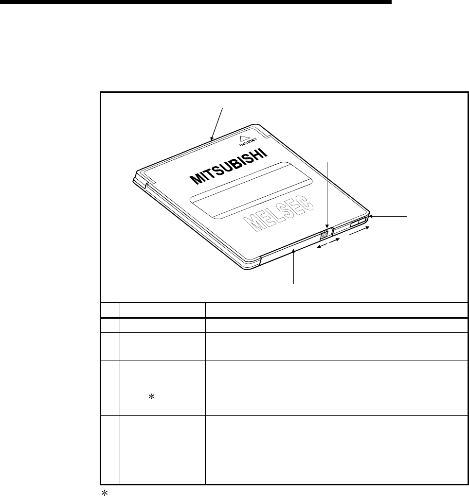
7 - 4 7 - 4
MELSEC-Q
7 MEMORY CARD AND BATTERY
7.4 The Names of The Parts of The Memory Card
The names of the parts of the memory card are described below.
Write-protected ON
2)
1)
4)
3)
"LOCK"
direction
"RELEASE"
direction
No. Name Descriptions
1) Connector area Connector area connected to the CPU module
2) Battery holder Used to set the lithium battery for data backup of the SRAM memory
(SRAM card only)
3) Battery holder fixing
switch
Switch for fixing the battery holder to the memory card main module
Locked at LOCK position (write protect switch side)
LOCK: Locked, RELEASE: Unlocked
(SRAM card only)
4) Write protect switch
Used to set write inhibit in the memory. At the time of shipping, it is
set at OFF.
(SRAM card and Flash card only)
ON: Data write inhibited
OFF: Data write enabled
: The battery holder fixing switch is returned automatically from RELEASE to LOCK
when the battery holder is disconnected.
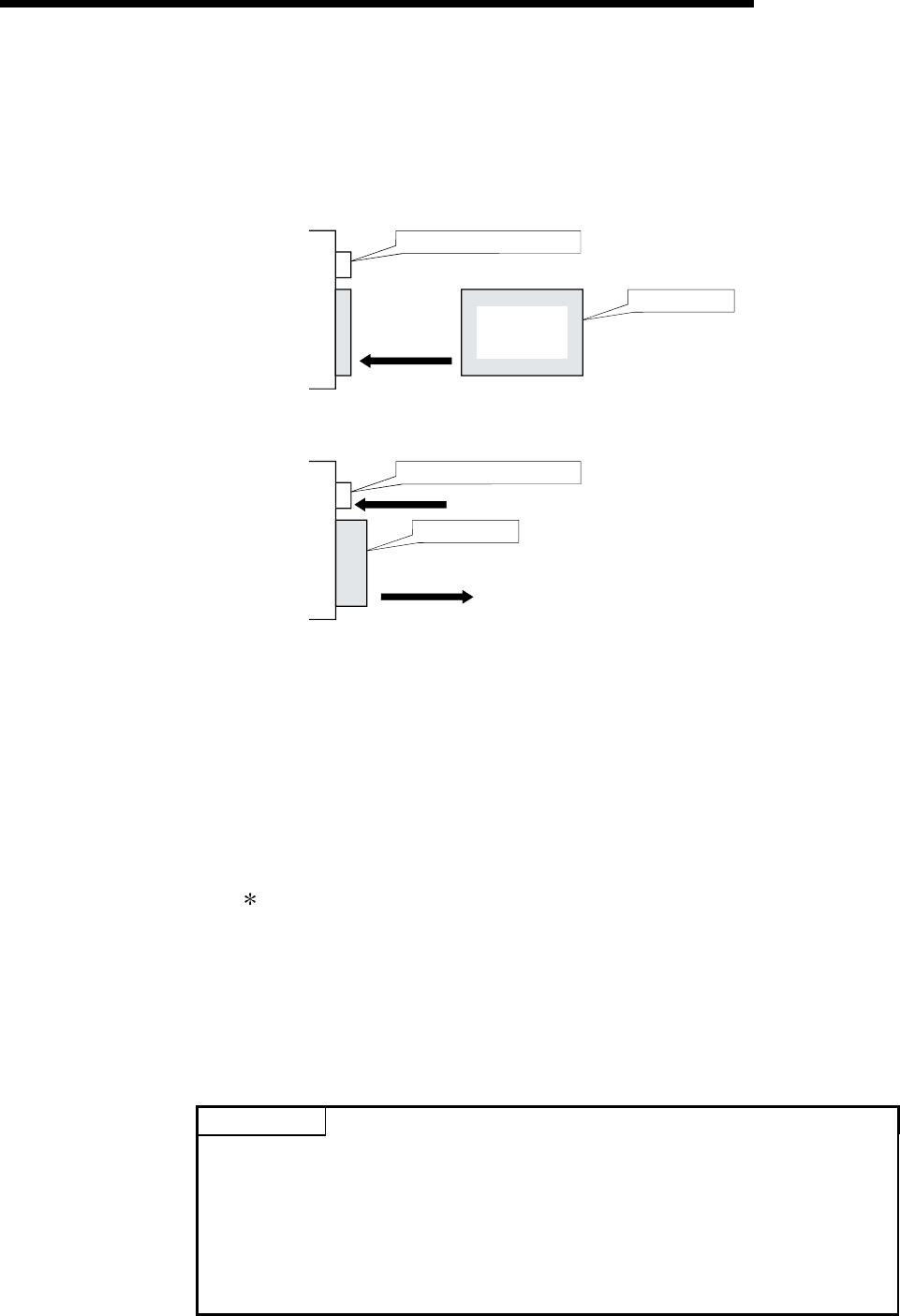
7 - 5 7 - 5
MELSEC-Q
7 MEMORY CARD AND BATTERY
7.5 Memory Card Loading/Unloading Procedures
(1) To install the memory card
Install the memory card into the CPU module, while paying attention to the
orientation of the memory card. Insert the memory card securely into the
connector until the height of the memory card reaches that of the memory card
EJECT button.
"Precautions"
on this side
Insert it in this
direction.
CPU
module
Memory card EJECT button
Memory card
(2) To remove the memory card
To remove the memory card from the CPU module, press the memory card
EJECT button to push out the card.
Remove the card
in this direction.
CPU
module
Push
Memory card EJECT button
Memory card
(3) To extract the memory card while the power is turned on
Before removing the memory card, make sure that the special relays "SM604",
"SM605" are OFF.
• When "SM604" is ON, the memory card cannot be removed since the CPU
module is using the memory card.
• When "SM605" is ON, turn it OFF.
When "SM604" and "SM605" are OFF, remove the memory card in the
following procedure.
1) Turn on the special relay "SM609" using the sequence program or by the
device test of GX Developer etc.
2) By monitoring GX Developer etc., check that the special relays "SM600" is
turned off.
3) Extract the memory card.
SM600 (Memory card usable flag) : The system is turned on when memory
card is ready for use by user.
SM604 (memory card use flag) : The system is turned on when the CPU
module uses a memory card.
SM605 (memory card detach inhibit flag) :
This is turned on by the user to disable
the memory card from being detached.
(4) To install the memory card while the power is turned on
1) Install the memory card.\
2) By monitoring GX Developer etc., check that the special relays "SM600" is
turned on.
POINTS
Install and remove the memory card while the power is turned on, paying
attention to the following.
(1) If the procedures specified above are not followed, the data stored in the
memory card may be destroyed.
When the CPU module operation at the time of occurrence of a parameter error
is set to STOP, the CPU module operation is stopped by the occurrence of
"ICM.OPE.ERROR."
(2) When the memory card is installed, its mount processing is performed again.
As a result, the scanning time is increased by several 10 ms max.
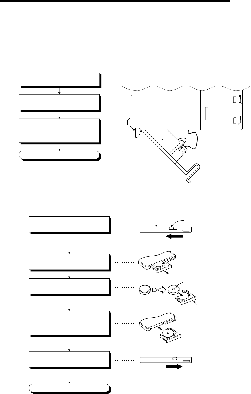
7 - 6 7 - 6
MELSEC-Q
7 MEMORY CARD AND BATTERY
7.6 Installation of Battery (for CPU Module and Memory Card)
(1) The battery for the CPU module is shipped with its connector disconnected.
Connect the connector as follows.
Refer to Section 10.3 for the service life of the battery and how to replace the
battery.
Side of the CPU module
Open the cover at the CPU module's
bottom.
Confirm that the battery is loaded
correctly.
Insert the battery connector into the
connector pin on the case. Be sure
that the insertion direction is correct.
Completion Connector
Bottom Battery
Front
(2) The battery for the SRAM card is shipped separately from the battery holder.
Before installing the SRAM card into the CPU module, set the battery holder in the
following procedure.
'+' sign
"LOCK" position
The battery holder's locking switch is set
automatically to the "LOCK" position when
the battery holder is removed. In its position,
insert the battery holder firmly.
Remove the battery holder from the
SRAM card.
Set the battery onto the battery
holder with the "plus" face up.
Insert the battery holder with which
the battery is installed firmly, into
the SRAM card.
Completion
Confirm that the battery holder's locking
switch is set to the "LOCK" position.
Set the battery holder's locking switch
to the "RELEASE" position.
"RELEASE" position
Battery holder's locking switch
"Model name"
on this side
Battery holder
8 - 1 8 - 1
MELSEC-Q
8 EMC AND LOW VOLTAGE DIRECTIVE
8 EMC AND LOW VOLTAGE DIRECTIVE
For the products sold in European countries, the conformance to the EMC Directive,
which is one of the European Directive, has been a legal obligation since 1996. Also,
conformance to the Low Voltage Directive, another European Directive, has been a
legal obligation since 1997.
Manufacturers who recognize their products must conform to the EMC and Low
Voltage Directive required to declare that their products conform to these Directives
and put a "CE mark" on their products.
8.1 Requirements for Conformance to EMC Directive
The EMC Directive specifies that products placed on the market must "be so
constructed that they do not cause excessive electromagnetic interference (emissions)
and are not unduly affected by electromagnetic interference (immunity)".
The applicable products are requested to meet these requirements. The sections 8.1.1
through 8.1.6 summarize the precautions on conformance to the EMC Directive of the
machinery constructed using the MELSEC-Q series PLCs.
The details of these precautions has been prepared based on the control requirements
and the applicable standards control. However, we will not assure that the overall
machinery manufactured according to these details conforms to the above-mentioned
directives. The method of conformance to the EMC Directive and the judgment on
whether or not the machinery conforms to the EMC Directive must be determined
finally by the manufacturer of the machinery.
8.1.1 Standards applicable to the EMC Directive
The standards applicable to the EMC Directive are listed below.
Specification Test item Test details Standard value
EN55011
Radiated noise 2
Electromagnetic emissions from the
product are measured.
30 M-230 MHz QP : 30 dB V/m
(30 m in measurement range) 1
230 M-1000 MHz QP : 37 dB V/m
(30 m in measurement range)
EN50081-2 :
1995
EN55011
Conducted noise
Electromagnetic emissions from the
product to the power line is
measured.
150 k-500 kHz QP : 79 dB, Mean : 66 dB 1
500 k-30 MHz QP : 73 dB, Mean : 60 dB
EN61000-4-2
Electrostatic immunity 2
Immunity test in which static
electricity is applied to the cabinet of
the equipment.
15 k V Aerial discharge
EN61000-4-4
Fast transient burst noise 2
Immunity test in which burst noise is
applied to the power line and signal
lines.
Power line : 2 kV
Digital I/O (24 V or higher) : 1 kV
(Digital I/O (24 V or less)) > 250 V
(Analog I/O, signal lines) > 250 V
EN61000-4-3
Radiated field AM
modulation 2
Immunity test in which field is
irradiated to the product.
10 V/m, 26-1000 MHz,
80%AM modulation@1 kHz
EN61131-2 :
1996
EN61000-4-12
Damped oscillatory wave
immunity
Immunity test in which a damped
oscillatory wave is superimposed on
the power line.
Power line : 1 kV
Digital I/O (24 V or higher) : 1 kV
(1) QP : Quasi-peak value, Mean : Average value
(2) The PLC is an open type device (device installed to another device) and must be installed in a conductive control panel.
The tests for the corresponding items were performed while the PLC was installed inside a control panel.
8

8 - 2 8 - 2
MELSEC-Q
8 EMC AND LOW VOLTAGE DIRECTIVE
8.1.2 Installation instructions for EMC Directive
The PLC is open equipment and must be installed within a control cabinet for use. This
not only ensures safety but also ensures effective shielding of PLC-generated
electromagnetic noise.
(1) Control cabinet
(a) Use a conductive control cabinet.
(b) When attaching the control cabinet's top plate or base plate, mask painting
and weld so that good surface contact can be made between the cabinet
and plate.
(c) To ensure good electrical contact with the control cabinet, mask the paint on
the installation bolts of the inner plate in the control cabinet so that contact
between surfaces can be ensured over the widest possible area.
(d) Earth the control cabinet with a thick wire so that a low impedance
connection to ground can be ensured even at high frequencies.
(e) Holes made in the control cabinet must be 10 cm (3.94 inch) diameter or
less. If the holes are 10 cm (3.94 inch) or larger, radio frequency noise may
be emitted.
In addition, because radio waves leak through a clearance between the
control panel door and the main unit, reduce the clearance as much as
practicable.
The leakage of radio waves can be suppressed by the direct application of
an EMI gasket on the paint surface.
Our tests have been carried out on a panel having the damping
characteristics of 37 dB max. and 30 dB mean (measured by 3 m method
with 30 to 300 MHz).
(2) Connection of power and earth wires
Earthing and power supply wires for the PLC system must be connected as
described below.
(a) Provide an earthing point near the power supply module. Earth the power
supply's LG and FG terminals (LG : Line Ground, FG : Frame Ground) with
the thickest and shortest wire possible. (The wire length must be 30 cm
(11.81 inch) or shorter.) The LG and FG terminals function is to pass the
noise generated in the PLC system to the ground, so an impedance that is
as low as possible must be ensured. As the wires are used to relieve the
noise, the wire itself carries a large noise content and thus short wiring
means that the wire is prevented from acting as an antenna.
(b) The earth wire led from the earthing point must be twisted with the power
supply wires. By twisting with the earthing wire, noise flowing from the power
supply wires can be relieved to the earthing. However, if a filter is installed
on the power supply wires, the wires and the earthing wire may not need to
be twisted.
8

8 - 3 8 - 3
MELSEC-Q
8 EMC AND LOW VOLTAGE DIRECTIVE
8.1.3 Cables
The cables extracted from the control panel contain a high frequency noise
component. On the outside of the control panel, therefore, they serve as antennas to
emit noise. To prevent noise emission, use shielded cable for the cables which are
connected to the I/O modules and intelligent function modules and may be extracted to
the outside of the control panel.
The use of a shielded cable also increases noise resistance. The signal lines
connected to the PLC I/O modules and intelligent function modules use shielded
cables to assure noise resistance under the conditions where the shield is earthed. If a
shielded cable is not used or not earthed correctly, the noise resistance will not meet
the specified requirements.
When the shield of a shielded cable is earthed to the cabinet body, please ensure that
the shield contact with the body is over a large surface area. If the cabinet body is
painted it will be necessary to remove paint from the contact area. All fastenings must
be metallic and the shield and earthing contact must be made over the largest
available surface area. If the contact surfaces are too uneven for optimal contact to be
made either use washers to correct for surface inconsistencies or use an abrasive to
level the surfaces. The following diagrams show examples of how to provide good
surface contact of shield earthing by use of a cable clamp.
(1) Earthing of shielded of shield cable
(a) Earth the shield of the shielded cable as near the module as possible taking
care so that the earthed cables are not induced electromagnetically by the
cable to be earthed.
(b) Take an appropriate measures so that the shield section of the shielded
cable from which the outer cover was partly removed for exposure is earthed
to the control panel on an increased contact surface. A clamp may also be
used as shown in the figure below. In this case, however, apply a cover to
the painted inner wall surface of the control panel which comes in contact
with the clamp.
Shield section
Screw
Clamp fittin
g
Shielded cable
Paint mask
Note) The method of earthing by soldering a wire onto the shield section of the
shielded cable as shown below is not recommended. The high frequency
impedance will increase and the shield will be ineffective.
Shielded cable
Wire
Crimp terminal
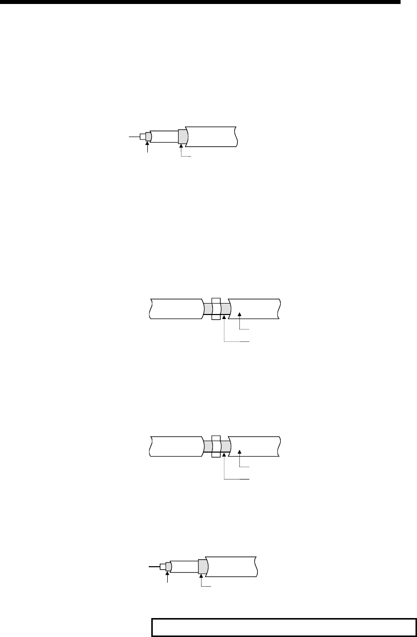
8 - 4 8 - 4
MELSEC-Q
8 EMC AND LOW VOLTAGE DIRECTIVE
(2) MELSECNET/H module
Always use a double-shielded coaxial cable (MITSUBISHI CABLE INDUSTRIES,
LTD.: 5C-2V-CCY) for the coaxial cables MELSECNET/H module. Radiated
noise in the range of 30MHz or higher can be suppressed by use of the double-
shielded coaxial cables. Earth the double-shielded coaxial cable by connecting its
outer shield to the ground.
Earth hereShield
Refer to (1) for the earthing of the shield.
(3) Ethernet module, Web server module
Precautions for using AUI cables, twisted pair cables and coaxial cables are
described below.
(a) Always earth the AUI cables connected to the 10BASE5 connectors.
Because the AUI cable is of the shielded type, strip part of the outer cover
and earth the exposed shield section to the ground on the widest contact
surface as shown below.
AUI cable
Shield
Refer to (1) for the earthing of the shield.
(b) Use shielded twisted pair cables as the twisted pair cables connected to the
10BASE-T/100BASE-TX connectors. For the shielded twisted pair cables,
strip part of the outer cover and earth the exposed shield section to the
ground on the widest contact surface as shown below.
Shielded twisted pair cables
Shield
Refer to (1) for the earthing of the shield.
(c) Always use double-shielded coaxial cables as the coaxial cables connected
to the 10BASE2 connectors. Earth the double-shielded coaxial cable by
connecting its outer shield to the ground.
Earth hereShield
Refer to (1) for the earthing of the shield.
Ethernet is the registered trademark of XEROX, Co., LTD.
(4) I/O signal lines and other communication cables
For the I/O signal lines and other communication cables lines (RS-232, RS-422, CC-
Link, etc.), if extracted to the outside of the control panel, also ensure to earth the
shield section of these lines and cables in the same manner as in item (1) above.
8 - 5 8 - 5
MELSEC-Q
8 EMC AND LOW VOLTAGE DIRECTIVE
8.1.4 Power supply module
Always ground the LG and FG terminals after short-circuiting them.
8.1.5 When using QA1S6 B type base unit
(1) Cable
(a) Earthing of shielded cable
• Earth the shield of the shielded cable as near the unit as possible taking
care so that the earthed cables are not induced electromagnetically by the
cable to be earthed.
• Take appropriate measures so the shield that was partly removed for
exposure is earthed to the control panel over a large contact surface area.
A clamp may also be used as shown in the figure below. In this case,
however, apply a cover to the painted inner wall surface of the control
panel which comes in contact with the clamp.
Shield section
Screw
Clamp fittin
g
Shielded cable
Paint mask
Note) The method of earthing by soldering a wire onto the shield section of the
shielded cable as shown below is not recommended. The high frequency
impedance will increase and the shield will be ineffective.
Shielded cable
Wire
Crimp terminal
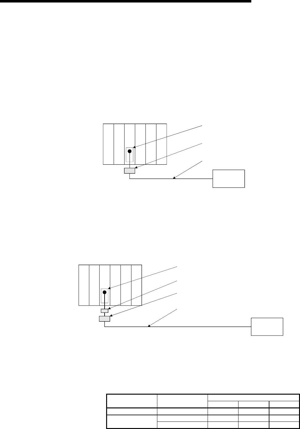
8 - 6 8 - 6
MELSEC-Q
8 EMC AND LOW VOLTAGE DIRECTIVE
(b) Positioning modules
Precautions to be followed when the machinery conforming to the EMC
Directive is configured using the A1SD75P1-S3/A1SD75P2-S3/A1SD75P3-
S3 (hereafter referred to as the A1SD75) are described below.
1) When wiring with a 2 m (6.56 ft.) or less cable
• Ground the shield section of the external wiring cable with the cable
clamp. (Ground the shield at the closest location to the A1SD75
external wiring connector.)
• Wire the external wiring cable to the drive unit and external device with
the shortest practicable length of cable.
• Install the drive unit in the same panel.
Power supply
module
A1SD75
module
Drive unit
External wiring connector
Cable clamp
External wiring cable (within 2 m (6.56 ft.))
2) When wiring with cable that exceeds 2 m (6.56 ft.), but is 10 m (32.79 ft.)
or less
• Ground the shield section of the external wiring cable with the cable
clamp. (Ground the shield at the closest location to the A1SD75
external wiring connector.)
• Install a ferrite core.
• Wire the external wiring cable to the drive unit and external device with
the shortest practicable length of cable.
External wiring connector
Ferrite core
External wiring cable (2 m to 10 m (6.56 ft. to 32.79 ft.))
Cable clamp
Power supply
module
A1SD75
module
Drive unit
3) Ferrite core and cable clamp types and required quantities
• Cable clamp
Type : AD75CK (Mitsubishi Electric)
• Ferrite core
Type : ZCAT3035-1330 (TDK ferrite core)
• Required quantity
Required Qty
Cable length Prepared part 1 axis 2 axes 3 axes
Within 2 m (6.56 ft.) AD75CK 1 1 1
AD75CK 1 1 1 2 m (6.56 ft.) to 10m
(32.79ft.) ZCAT3035-1330 1 2 3
8 - 7 8 - 7
MELSEC-Q
8 EMC AND LOW VOLTAGE DIRECTIVE
(c) CC-Link module
1) Be sure to ground the cable shield that is connected to the CC-Link
module close to the exit of control panel or to any of the CC-Link stations
within 30 cm (11.81 inch) from the module or stations.
The CC-Link dedicated cable is a shielded cable. As shown in the
illustration below, remove a portion of the outer covering and ground as
large a surface area of the exposed shield part as possible.
CC-Link dedicated cable
Shield
2) Always use the specified CC-Link dedicated cable.
3) Do not use a ferrite core for the CC-Link module or CC-Link stations.
4) The CC-Link module, the CC-Link stations and the FG line inside the
control panel should be connected at both the FG terminal and the SLD
terminal as shown in the diagram below.
[Simplified diagram]
T
erminal resistor
Master station Remote I/O station Local station
Terminal resisto
r
CC-Link
dedicated
cable
CC-Link
dedicated
cable
DA
DB
DG
SLD
FG
DA
DB
DG
SLD
FG
DA
DB
DG
SLD
FG
(Blue)
(White)
(Yellow)
(d) I/O signal lines
For the I/O signal lines, if extracted to the outside of the control panel, also
ensure to earth the shield section of these lines and cables in the same
manner as in item (1) above.
(2) Power supply module
The precautions required for each power supply module are described below.
Always observe the items noted as precautions.
Model Precautions
A1S61P
A1S62P Not usable
A1S63P ( 1) Use the CE marked 24VDC panel power equipment.
A1S61PEU
A1S62PEU
A1S61PN
A1S62PN
Always ground the LG and FG terminals after short-circuiting them.
(1) If sufficient filter circuitry is built into the 24VDC external power supply module, the noise
generated by A1S63P will be absorbed by that filter circuit, so a line filter may not be
required.
Filtering circuitry of version F or later of A1S63P is improved so that a external line filter is
not required.
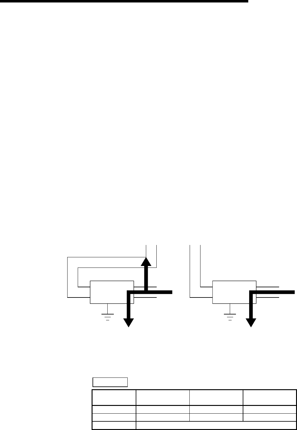
8 - 8 8 - 8
MELSEC-Q
8 EMC AND LOW VOLTAGE DIRECTIVE
8.1.6 Others
(1) Ferrite core
A ferrite core has the effect of reducing radiated noise in the 30MHz to 100MHz
band.
It is not required to fit ferrite cores to cables, but it is recommended to fit ferrite
cores if shield cables pulled out of the enclosure do not provide sufficient
shielding effects.
It should be noted that the ferrite cores should be fitted to the cables in the
position immediately before they are pulled out of the enclosure. If the fitting
position is improper, the ferrite will not produce any effect.
In the CC-Link system, however, ferrite cores cannot be fitted to cables.
(2) Noise filter (power supply line filter)
A noise filter is a component which has an effect on conducted noise.
It is not required to fit the noise filter to the power supply line, but fitting it can
further suppress noise.
(The noise filter has the effect of reducing conducted noise of 10 MHz or less.)
The precautions required when installing a noise filter are described below.
(a) Do not bundle the wires on the input side and output side of the noise filter.
When bundled, the output side noise will be induced into the input side wires
from which the noise was filtered.
Input side
(power supply side)
Output side
(device side)
Introduction
Filter
Output side
(device side)
Filter
Input side
(power supply side)
1) The noise will be included when the
input and output wires are bundled.
2) Separate and lay the input
and output wires.
(b) Earth the noise filter earthing terminal to the control cabinet with the shortest
wire possible (approx. 10 cm (3.94 inch)).
Reference
Noise Filter
Model Name FN343-3/01 FN660-6/06 ZHC2203-11
Manufacturer SCHAFFNER SCHAFFNER TDK
Rated current 3 A 6 A 3 A
Rated voltage 250 V

8 - 9 8 - 9
MELSEC-Q
8 EMC AND LOW VOLTAGE DIRECTIVE
8.2 Requirement to Conform to the Low Voltage Directive
The Low Voltage Directive requires each device that operates with the power supply
ranging from 50 to 1000VAC and 75 to 1500VDC to satisfy the safety requirements.
In Sections 8.2.1 to 8.2.6, cautions on installation and wiring of the MELSEC-Q series
PLC to conform to the Low Voltage Directive are described.
We have put the maximum effort to develop this material based on the requirements
and standards of the regulation that we have collected. However, compatibility of the
devices which are fabricated according to the contents of this manual to the above
regulation is not guaranteed. Each manufacturer who fabricates such device should
make the final judgement about the application method of the Low Voltage Directive
and the product compatibility.
8.2.1 Standard applied for MELSEC-Q series PLC
The standard applied for MELSEC-Q series PLC is EN61010-1 safety of devices used
in measurement rooms, control rooms, or laboratories.
The MELSEC-Q series PLC modules which operate at the rated voltage of
50VAC/75VDC or above are also developed to conform to the above standard.
The modules which operate at the rated voltage of less than 50VAC/75VDC are out of
the Low Voltage Directive application range.
8.2.2 MELSEC-Q series PLC selection
(1) Power supply module
There are dangerous voltages (voltages higher than 42.4V peak) inside the
power supply modules of the 100/200VAC rated I/O voltages. Therefore, the CE
marked models are enhanced in insulation internally between the primary and
secondary.
(2) I/O module
There are dangerous voltages (voltages higher than 42.4V peak) inside the I/O
modules of the 100/200VAC rated I/O voltages. Therefore, the CE marked
models are enhanced in insulation internally between the primary and secondary.
The I/O modules of 24VDC or less rating are out of the Low Voltage Directive
application range.
(3) CPU module, memory card, base unit
Using 5VDC circuits inside, the above modules are out of the Low Voltage
Directive application range.
(4) Intelligent function modules (special function modules)
The intelligent function modules (special function modules) such as the analog,
network and positioning modules are 24VDC or less in rated voltage and are
therefore out of the Low Voltage Directive application range.
(5) Display device
Use the CE marked display device.
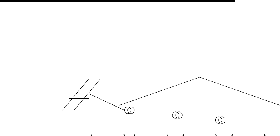
8 - 10 8 - 10
MELSEC-Q
8 EMC AND LOW VOLTAGE DIRECTIVE
8.2.3 Power supply
The insulation specification of the power supply module was designed assuming
installation category II. Be sure to use the installation category II power supply to the
PLC.
The installation category indicates the durability level against surge voltage generated by
a thunderbolt. Category I has the lowest durability; category IV has the highest durability.
Category III Category II Category ICategory IV
Figure 8.1: Installation Category
Category II indicates a power supply whose voltage has been reduced by two or more
levels of isolating transformers from the public power distribution.
8.2.4 Control box
Because the PLC is an open device (a device designed to be stored within another
module), be sure to use it after storing in the control box.
(1) Electrical shock prevention
In order to prevent persons who are not familiar with the electric facility such as
the operators from electric shocks, the control box must have the following
functions :
(a) The control box must be equipped with a lock so that only the personnel who
has studied about the electric facility and have enough knowledge can open it.
(b) The control box must have a structure which automatically stops the power
supply when the box is opened.
(2) Dustproof and waterproof features
The control box also has the dustproof and waterproof functions. Insufficient
dustproof and waterproof features lower the insulation withstand voltage, resulting
in insulation destruction. The insulation in our PLC is designed to cope with the
pollution level 2, so use in an environment with pollustion level 2 or below.
Pollution level 1 : An environment where the air is dry and conductive
dust does not exist.
Pollution level 2 : An environment where conductive dust
does not usually exist, but occasional temporary
conductivity occurs due to the accumulated dust. Generally,
this is the level for inside the control box equivalent to IP54
in a control room or on the floor of a typical factory.
Pollution level 3 : An environment where conductive dust exits and conductivity
may be generated due to the accumulated dust.
An environment for a typical factory floor.
Pollution level 4 : Continuous conductivity may occur due to rain, snow,
etc. An outdoor environment.
As shown above, the PLC can realize the pollution level 2 when stored in a
control box equivalent to IP54.
8 - 11 8 - 11
MELSEC-Q
8 EMC AND LOW VOLTAGE DIRECTIVE
8.2.5 Grounding
There are the following two different grounding terminals.
Use either grounding terminal in an earthed status.
Protective grounding : Maintains the safety of the PLC and improves the
noise resistance.
Functional grounding : Improves the noise resistance.
8.2.6 External wiring
(1) 24VDC external power supply
For the MELSEC-Q series PLC 24VDC I/O modules and the intelligent function
modules (special function modules) which require external supply power, use a
model whose 24VDC circuit is intensively insulated from the hazardous voltage
circuit.
(2) External devices
When a device with a hazardous voltage circuit is externally connected to the
PLC, use a model whose circuit section of the interface to the PLC is intensively
insulated from the hazardous voltage circuit.
(3) Intensive insulation
Intensive insulation refers to the insulation with the dielectric withstand voltage
shown in Table 8.1.
Table 8.1 : Intensive Insulation Withstand Voltage
(Installation Category II, source : IEC664)
Rated voltage of hazardous voltage area Surge withstand voltage (1.2/50 s)
150VAC or below 2500 V
300VAC or below 4000 V
9 - 1 9 - 1
MELSEC-Q
9 LOADING AND INSTALLATION
9 LOADING AND INSTALLATION
In order to increase the reliability of the system and exploit the maximum performance
of its functions, this section describes the methods and precautions for the mounting
and installation of the system.
9.1 General Safety Requirements
! DANGER Install a safety circuit external to the PLC that keeps the entire
system safe even when there are problems with the external power
supply or the PLC module. Otherwise, trouble could result from
erroneous output or erroneous operation.
(1) Outside the PLC, construct mechanical damage preventing
interlock circuits such as emergency stop, protective circuits,
positioning upper and lower limits switches and interlocking
forward/reverse operations.
(2) When the PLC detects the following problems, it will stop
calculation and turn off all output in the case of (a).
In the case of (b), it will stop calculation and hold or turn off all
output according to the parameter setting.
Note that the A1S series module will turn off the output in either
of cases (a) and (b).
All outputs of AnS Series Module will be switched off in the
following cases:
(a) The power supply module has over current protection
equipment and over voltage protection equipment.
(b) The PLC CPUs self-diagnosis functions, such as the watch
dog timer error, detect problems.
In addition, all output will be turned on when there are problems
that the PLC CPU cannot detect, such as in the I/O controller.
(3) Output could be left on or off when there is trouble in the outputs
module relay or transistor. So build an external monitoring circuit
that will monitor any single outputs that could cause serious
trouble.
When overcurrent which exceeds the rating or caused by short-
circuited load flows in the output module for a long time, it may
cause smoke or fire. To prevent this, configure an external safety
circuit, such as fuse.
Build a circuit that turns on the external power supply when the PLC
main module power is turned on. If the external power supply is
turned on first, it could result in erroneous output or erroneous
operation.
When there are communication problems with the data link, refer to
the corresponding data link manual for the operating status of each
station. Not doing so could result in erroneous output or erroneous
operation.operating status of each station. Not doing so could result
in erroneous output or erroneous operation.
9
9 - 2 9 - 2
MELSEC-Q
9 LOADING AND INSTALLATION
! DANGER When connecting a peripheral device to the CPU module or connecting
a personal computer or the like to the special function module to
exercise control (data change) on the running PLC, configure up an
interlock circuit in the sequence program to ensure that the whole
system will always operate safely.
Also before exercising other control (program change, operating status
change (status control)) on the running PLC, read the manual carefully
and fully confirm safety.
Especially for the above control on the remote PLC from an external
device, an immediate action may not be taken for PLC trouble due to a
data communication fault.
In addition to configuring up the interlock circuit in the sequence
program, corrective and other actions to be taken as a system for the
occurrence of a data communication fault should be predetermined
between the external device and PLC CPU.
! CAUTION Do not bunch the control wires or communication cables with the main
circuit or power wires, or install them close to each other. They should
be installed 100 mm (3.94 inch) or more from each other.
Not doing so could result in noise that would cause erroneous
operation.
When controlling items like lamp load, heater or solenoid valve using an
output module, large current (approximately ten times greater than that
present in normal circumstances) may flow when the output is turned
OFF to ON. Take measures such as replacing the module with one
having sufficient rated current.
When the PLC power supply is switched ON-OFF, correct control output may not be
performed temporarily due to differences in delay time and starting time between the
PLC power supply and the external power supply for the controlled object (especially
DC).
For example, if the external power supply for the controlled object is switched on in a
DC output module and then the PLC power supply is switched on, the DC output
module may provide false output instantaneously at power-on of the PLC. Therefore, it
is necessary to make up a circuit that can switch on the PLC power supply first.
Also, an abnormal operation may be performed if an external power supply fault or
PLC failure takes place.
To prevent any of these abnormal operations from leading to the abnormal operation of
the whole system and in a fail-safe viewpoint, areas which can result in machine
breakdown and accidents due to abnormal operations (e.g. emergency stop, protective
and interlock circuits) should be constructed outside the PLC.
The following page gives examples of system designing in the above viewpoint.
9
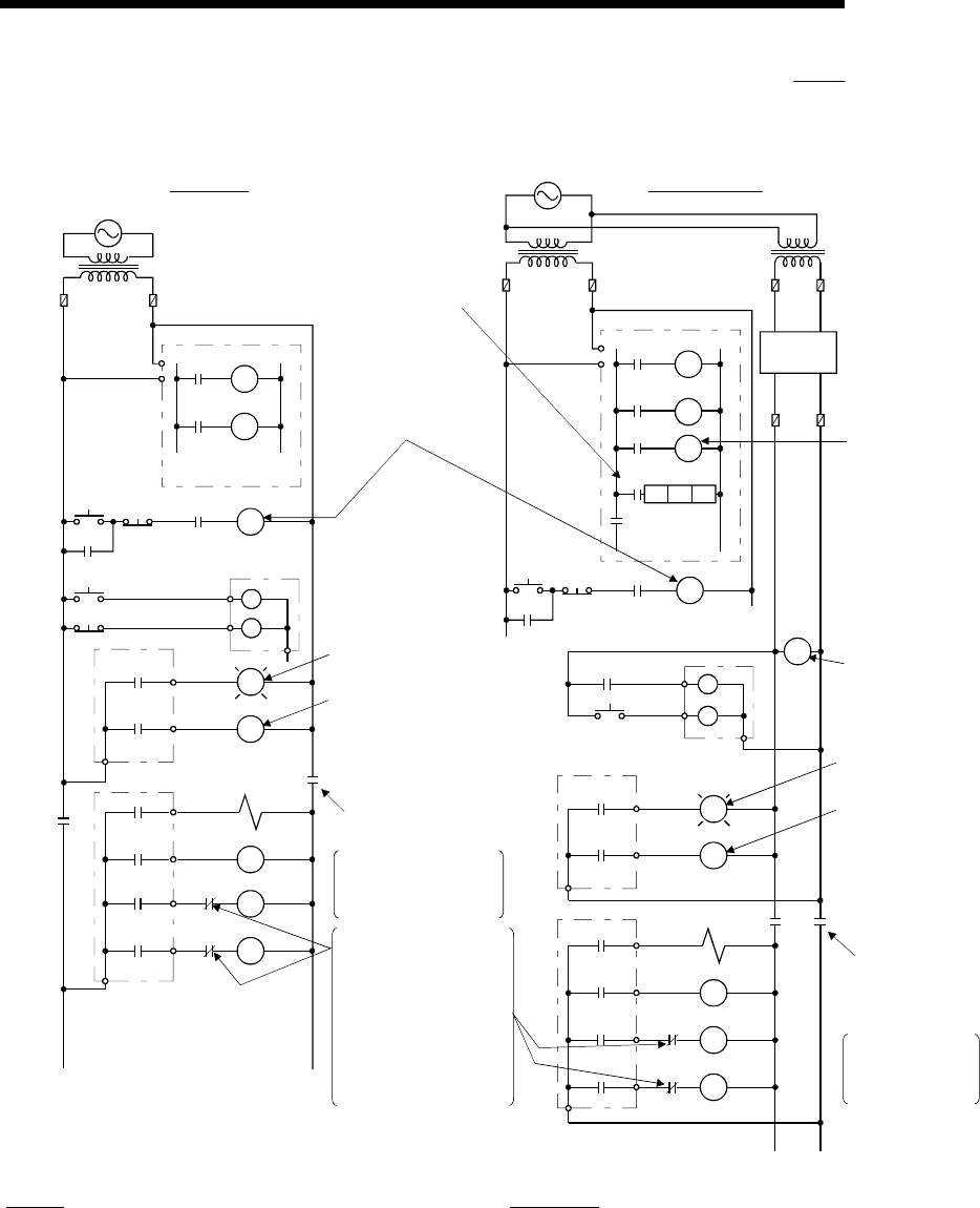
9 - 3 9 - 3
MELSEC-Q
9 LOADING AND INSTALLATION
(1) System design circuit example (when not using ERR contact of
power supply module)
START
SW
STOP
SW
MC
RA1 MC
RA2
RA2
XM
L
Ym
Yn
OUTPUT MODULE
MC2
MC1
MC1
RA1
M10
PROGRAM
CPU MODULE
NO
TRANSFORMER
FUSE FUSE
POWER
SUPPLY
POWER
SUPPLY
TRANSFORMER
FUSE
DC
POWER
SUPPLY
FUSE
MC2
MC MC
In the case of an
emergency stop or a
stop caused by a limit
switch.
Interlock circuits as
necessary.Provide
external interlock
circuits for conflicting
operations, such as
forward rotation and
reverse rotation, and
for parts that could
damage the machine
or cause accidents if
no interlock were used.
Power to output equipment
switched OFF when the
STOP signal is given.
In the case of an
emergency stop
or a stop caused
by a limit switch.
Power to output
equipment
switched OFF
when the STOP
signal is given.
Ym
SM52
SM52
SM403 SM403
TM
XM
MC1 NO M10
TM
MC1
MC2
MC
MC2
MC1
OUTPUT MODULE
L
RA1
Ym
Yn
INPUT MODULE
START
SW
STOP
SW
MC
RA1 MC
PROGRAM
Low battery alarm
(Lamp or buzzer)
RA1 switched ON by
SM403
(run monitor relay)
RUN/STOP circuit
interlocked with RA1
(run monitor relay)
Input switched
when power
supply
established.
ON when run by
SM403
Low battery alarm
(Lamp or buzzer)
Voltage relay is
recommended
Set time for DC
power supply to
be established.
FOR AC/DCFOR AC
CPU MODULE
Ym
Yn
(-) (+)
MC
Yn
OUTPUT MODULE
TRANSFORMER
OUTPUT MODULE
The power-ON procedure is as follows:
For AC For AC/DC
1) Switch power ON.
2) Set CPU to RUN.
3) Turn ON the start switch.
4) When the magnetic contactor (MC) comes on, the output
equipment is powered and may be driven by the program.
1) Switch power ON.
2) Set CPU to RUN.
3) When DC power is established, RA2 goes ON.
4) Timer (TM) times out after the DC power reaches 100%.
(The TM set value should be the period of time from when
RA2 goes ON to the establishment of 100% DC voltage.
Set this value to approximately 0.5 seconds.)
5) Turn ON the start switch.
6) When the magnetic contactor (MC) comes on, the output
equipment is powered and may be driven by the program.
(If a voltage relay is used at RA2, no timer (TM) is required
in the program.)
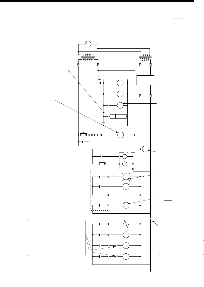
9 - 4 9 - 4
MELSEC-Q
9 LOADING AND INSTALLATION
(2) System design circuit example (when using ERR contact of power
supply module)
STRAT
SW
STOP
SW
MC
RA1 MC
RA2
RA2
XM
L
Ym
OUTPUT MODULE
MC2
MC1
MC1
RA3
M10
PROGRAM
CPU MODULE
NO
TRANSFORMER
FUSE
TRANSFORMER
POWER
SUPPLY
DC
POWER
SUPPLY
MC2
MC MC
Interlock circuits asnecessary.
Provide external interlock
circuits for conflicting operations,
such as forward rotation and
reverse rotation, and for parts
that could damage the machine
or cause accidents if no interlock
were used.
In the case of an
emergency stop or a stop
caused by a limit switch.
Ym
SM52
TM
XM
MC1 NO M10
TM
RUN/STOP circuit
interlocked with
RA1
(run monitor relay)
Input switched
when power
supply
established.
Low battery alarm
(Lamp or buzzer)
Voltage relay is
recommended
Set time for DC
power supply to
be established.
FOR AC/DC
(-)(+)
ERR OFF at stop error
from ERR
POWER SUPPLY
MODULE
Yn
SM403
RA3
RA1
Yn
Power to output equipment
switched OFF when ERR
contact turns OFF.
FUSE
FUSE
OUTPUT MODULE
The power-ON procedure is as follows:
For AC/DC
1) Switch power ON.
2) Set CPU to RUN.
3) When DC power is established, RA2 goes ON.
4) Timer (TM) times out after the DC power reaches 100%. (The TM set value should be the period of time
from when RA2 goes ON to the establishment of 100% DC voltage. Set this value to approximately 0.5s.)
5) Turn ON the start switch.
6) When the magnetic contactor (MC) comes on, the output equipment is powered and may be driven by the
program. (If a voltage relay is used at RA2, no timer (TM) is required in the program.)
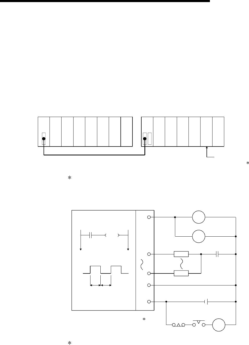
9 - 5 9 - 5
MELSEC-Q
9 LOADING AND INSTALLATION
(3) Fail-safe measures against failure of the PLC
Failure of a CPU module or memory can be detected by the self-diagnosis
function. However, failure of I/O control area may not be detected by the CPU
module.
In such cases, all I/O points turn ON or OFF depending on a condition of
problem, and normal operating conditions and operating safety cannot
sometimes be maintained.
Though Mitsubishi PLCs are manufactured under strict quality control, they may
cause failure or abnormal operations due to unspecific reasons. To prevent the
abnormal operation of the whole system, machine breakdown, and accidents,
fail-safe circuitry against failure of the PLC must be constructed outside the PLC.
Examples of a system and its fail-safe circuitry are described below:
<System example>
Power supply
module
CPU module
Input 16 points
Vacant
Input 16 points
Input 16 points
Input 16 points
Output 16 points
Y80 to Y8F
Output 16 points
Output 16 points
Output 16 points
Output 16 points
Output module for
fail-safe purpose 1
Power supply
module
1: The output module for fail-safe purpose should be loaded in the last slot of
the system. (Y80 to Y8F in the above system.)
<Fail-safe circuit example>
Internal program
SM412
T1
ON delay timer
1s
T2
OFF delay timer
1s
L
L
MC
T2T1
+
-
24V DC
Y80
Y81
Y8F
24V
0V
Y80
Y80
External load
0.5s0.5s
CPU module
MC
Output module
2
2: Y80 repeats turning ON and then OFF at 0.5s intervals.
Use a no-contact output module (transistor in the example shown above).

9 - 6 9 - 6
MELSEC-Q
9 LOADING AND INSTALLATION
9.2 Calculating Heat Generation by PLC
The ambient temperature inside the board storing the PLC must be suppressed to a
PLC usable ambient temperature of 55°C.
For the design of radiation from the storing board, it is necessary to know the average
power consumption (heating value) of the devices and instruments stored in the board.
Here the method of obtaining the average power consumption of the PLC system is
described.
From the power consumption, calculate a rise in ambient temperature inside the board.
How to calculate average power consumption
The power consuming parts of the PLC are roughly classified into six
blocks as shown below.
(1) Power consumption of power supply module
The power conversion efficiency of the power supply module is approx. 70 %,
i.e., 30 % of the output power is consumed by heating. As a result, 3/7 of the
output power becomes the power consumption.
Therefore the calculation formula is as follows.
Wpw = (I5v 5) (W)
3
7
I5V: Current consumption of logic 5 VDC circuit of each module
(2) Power consumption of a total of 5 VDC logic section of each
module
The power consumption of the 5 VDC output circuit section of the power supply
module is the power consumption of each module (including the current
consumption of the base unit).
W5V = I5V 5 (W)
(3)
A total of 24 VDC average power consumption of the output module
(power consumption for simultaneous ON points)
The average power of the external 24 VDC power is the total power consumption
of each module.
W24V = I24V 24 (W)
(4) Average power consumption due to voltage drop in the output
section of the output module
(Power consumption for simultaneous ON points)
WOUT = IOUT Vdrop Number of outputs Simultaneous ON rate (W)
IOUT : Output current (Current in actual use) (A)
Vdrop : Voltage drop in each output module (V)
(5) Average power consumption of the input section of the input
module(Power consumption for simultaneous ON points)
WIN = IIN E Number of input points Simultaneous ON rate (W)
IIN : Input current (Effective value for AC) (A)
E : Input voltage (Voltage in actual use) (V)
9 - 7 9 - 7
MELSEC-Q
9 LOADING AND INSTALLATION
(6) Power consumption of the power supply section of the intelligent
function module
WS = I5V 5 + I24V 24 + I100V 100 (W)
The total of the power consumption values calculated for each block becomes
the power consumption of the overall sequencer system.
W = WPW + W5V + W24V + WOUT + WIN + WS (W)
From this overall power consumption (W), calculate the heating value and a rise
in ambient temperature inside the board.
The outline of the calculation formula for a rise in ambient temperature inside the
board is shown below.
T = W
UA (°C)
W : Power consumption of overall sequencer system (value obtained above)
A : Surface area inside the board
U :
When the ambient temperature inside the board is uniformed by a fan
.........6
When air inside the board is not circulated..............................................4
POINT
When a rise in ambient temperature inside the board exceeds the specified limit, it
is recommended that you install a heat exchanger in the board to lower the ambient
temperature inside the board.
If a normal ventilating fan is used, dust will be sucked into the PLC together with
the external air, and it may affect the performance of the PLC.
(7) Example of calculation of average power consumption
(a) System configuration
Q35B
Q61P-A1
Q02HCPU
QX40
QX40
QY10
QJ71LP21-25
Vacant
(b) 5 VDC current consumption of each module
Q02HCPU : 0.64 (A)
QX40 : 0.05 (A)
QY10 : 0.43 (A)
QJ71LP21-25 : 0.55 (A)
Q35B : 0.074 (A)
(c) Power consumption of power supply module
WPW = 3/7 (0.64+0.05+0.05+0.43+0.55+0.074) 5) = 3.84 (W)
(d) Power consumption of a total of 5 VDC logic section of each module
W5V = (0.64+0.05+0.05+0.43+0.55+0.074) 5) = 8.97 (W)
(e) A total of 24 VDC average power consumption of the output module
W24V = 0 (W)

9 - 8 9 - 8
MELSEC-Q
9 LOADING AND INSTALLATION
(f) Average power consumption due to voltage drop in the output section of the
output module
WOUT = 0 (W)
(g) Average power consumption of the input section of the input module
WIN = 0.004 24 32 1 = 3.07 (W)
(h) Power consumption of the power supply section of the intelligent function
module
WS = 0 (W)
(i) Power consumption of overall system.
W = 3.84 + 8.97 + 0 + 0 + 3.07 + 0 = 15.88 (W)
9 - 9 9 - 9
MELSEC-Q
9 LOADING AND INSTALLATION
9.3 Module Installation
9.3.1 Precaution on installation
! CAUTION Use the PLC in an environment that meets the general specifications
contained in this manual. Using this PLC in an environment outside the
range of the general specifications could result in electric shock, fire,
erroneous operation, and damage to or deterioration of the product.
Hold down the module loading lever at the module bottom, and
securely insert the module fixing latch into the fixing hole in the base
unit. Incorrect loading of the module can cause a malfunction, failure or
drop.When using the PLC in the environment of much vibration, tighten
the module with a screw.
Tighten the screw in the specified torque range. Undertightening can
cause a drop, short circuit or malfunction. Overtightening can cause a
drop, short circuit or malfunction due to damage to the screw or
module.
When installing more cables, be sure that the base unit and the module
connectors are installed correctly. After installation, check them for
looseness. Poor connections could cause an input or output failure.
Securely load the memory card by pushing it into the memory card
loading slot. Check for insecure loading after loading the memory card.
Not doing so can cause a malfunction due to a contact fault.
Completely turn off the external power supply before loading or
unloading the module. Not doing so could result in electric shock or
damage to the product.
Do not directly touch the module's conductive parts or electronic
components. Touching the conductive parts could cause an operation
failure or give damage to the module.
This section gives instructions for handling the CPU, I/O, intelligent function and power
supply modules, base units and so on.
(1) Module enclosure, terminal block connectors and pin connectors are made of resin;
do not drop them or subject them to strong impact.
(2) Do not remove modules' printed circuit boards from the enclosure in order to avoid
changes in operation.
(3) Tighten the module fixing screws and terminal block screws within the tightening
torque range specified below.
Location of Screw Tightening Torque Range
Module fixing screw (M3 12 screw) 36 to 48 N • cm
I/O module terminal block screw (M3 screw) 42 to 58 N • cm
I/O module terminal block fixing screw (M3.5 screw) 66 to 89 N • cm
Power supply module terminal screw (M3.5 screw) 66 to 89 N • cm
(4) Be sure to install the power supply module in the Q3 B, Q6 B and QA1S6 B.
Even if the power supply module is not installed, when the I/O modules and
intelligent function module installed on the base units are of light load type, the
modules may be operated. In this case, because a voltage becomes unstable, we
cannot guarantee the operation.
(5) When an extension cable is used, do not bind the cable together with the main
circuit (high voltage, heavy current) line or lay them close to each other.
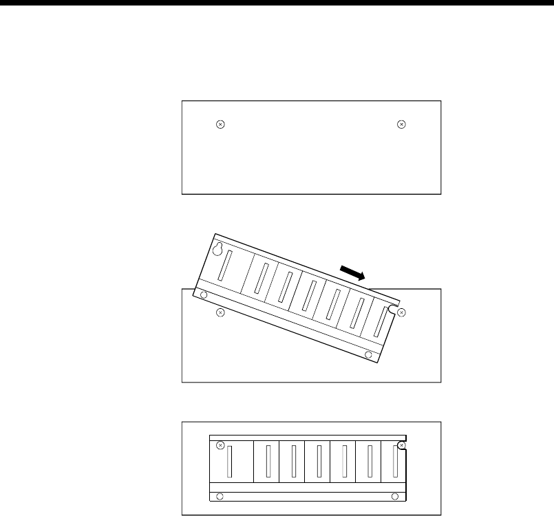
9 - 10 9 - 10
MELSEC-Q
9 LOADING AND INSTALLATION
(6) Install the main base unit (by screwing) in the following procedure.
1) Fit the two base unit top mounting screws into the enclosure.
Panel
2) Place the right-hand side notch of the base unit onto the right-hand side screw.
Panel
3) Place the left-hand side pear-shaped hole onto the left-hand side screw.
Panel
4) Fit the mounting screws into the mounting screw holes in the base unit bottom
and retighten the four mounting screws.
Note1 : Install the main base unit to a panel, with no module loaded in the right-end
slot.
Remove the base unit after unloading the module from the right-end slot.
Note2 : The mounting screws that included with the slim type main base unit differ
from those included with other types of the base unit. When ordering
mounting screws for the slim type main base unit, specify "cross recessed
head bind screw M4 x 12 (black)."
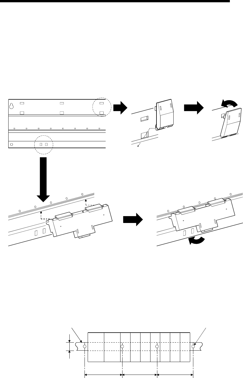
9 - 11 9 - 11
MELSEC-Q
9 LOADING AND INSTALLATION
(7) Note the following points when mounting a DIN rail.
Mounting a DIN rail needs special adaptors (optional), which are to be user-
prepared.
(a) Applicable adaptor types
For Q38B, Q312B, Q68B, Q612B : Q6DIN1
For Q35B, Q65B : Q6DIN2
For Q33B, Q52B, Q55B, Q63B, Q32SB, Q33SB, Q35SB : Q6DIN3
(b) Adaptor installation method
The way to install the adaptors for mounting a DIN rail to the base unit is given
below.
Base unit rear
Place the hook of the adaptor
(small) in the lower hole.
Push the top of the adaptor
(small) far enough until it
"clicks".
Insert the adaptor (large) into the grooves
of the base unit from below.
Push the bottom of the adaptor (large) far
enou
g
h until it "clicks".
(c) Applicable DIN rail types (JIS C 2812)
TH35-7.5Fe
TH35-7.5Al
TH35-15Fe
(d) DIN rail mounting screw intervals
When using a TH35-7.5Fe or TH35-7.5Al DIN rail, rail mounting screws should
be tightened at a pitch of 200 mm (7.88 inch) or less in order to ensure that the
rail has sufficient strength.
35mm
(1.38 inch)
P=2
00
mm
(
7.
88
in
c
h
)
o
r l
ess
DIN rail DIN rail mounting screw
PPP
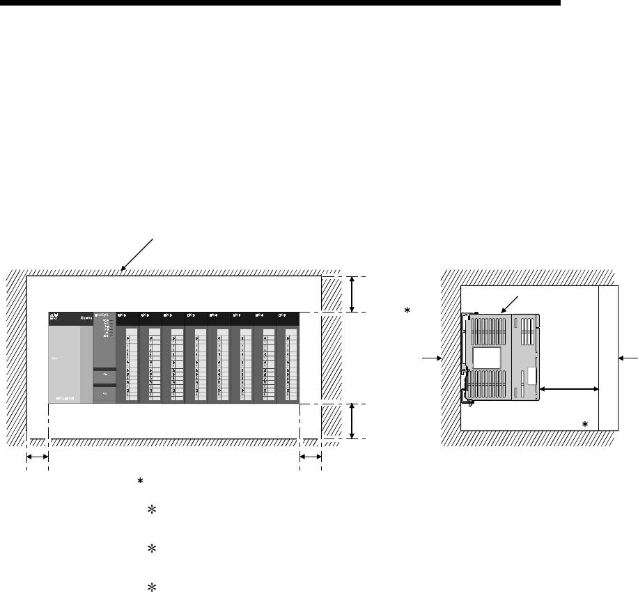
9 - 12 9 - 12
MELSEC-Q
9 LOADING AND INSTALLATION
9.3.2 Instructions for mounting the base unit
When mounting the PLC to an enclosure or similar, fully consider its operability,
maintainability and environmental resistance.
(1) Module mounting position
For enhanced ventilation and ease of module replacement, leave the following
clearances between the module top/bottom and structure/parts.
(a) In case of main base unit or extension base unit
Indicates the panel top, wiring
duct or any part position.
PLC
DoorPanel
20mm
(0.79 inch)
or more 3
5mm (0.20 inch) or more 2 5mm (0.20 inch) or more
30mm
(1.18 inch)
or more 1
30mm
(1.18 inch)
or more
1 : For wiring duct with 50mm (1.97 inch) or less height.
40mm (1.58 inch) or more for other cases.
2 : 20mm (0.79 inch) or more when the adjacent module is not removed and the
extension cable is connected.
3 : 80mm (3.15 inch) or more for the connector type.
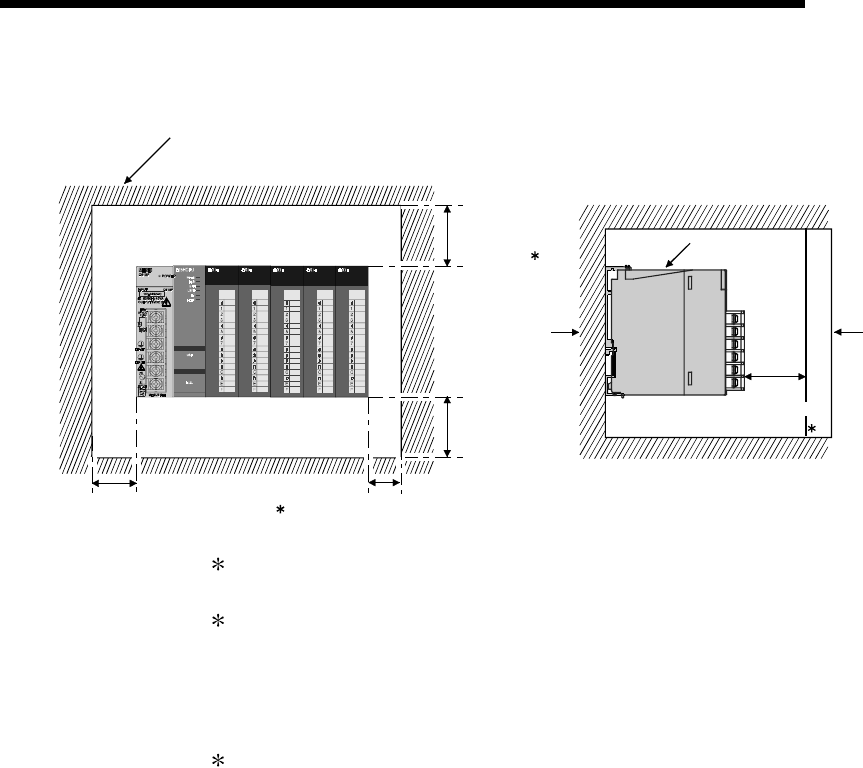
9 - 13 9 - 13
MELSEC-Q
9 LOADING AND INSTALLATION
(b) In case of slim type main base unit
PLC
Door
30 mm
(1.18 inch)
or more
5 mm (0.20 inch) or more
30 mm
(1.18 inch)
or more 1
17 mm (0.67 inch) or more 2
3
20 mm
(0.79 inch)
or more
Panel
Indicates the panel top, wiring
duct or any part position.
1 : For wiring duct with 50 (1.97 inch) mm or less height.
40 mm (1.58 inch) or more for other cases.
2 : The cable of the power supply module of the slim type main base unit protrudes
out of the left end of the module. Install the module while reserving 17 mm (0.67
inch) or more wiring space. If the cable sheath is susceptible to damage caused
by a structural object or part on the left side of the module, take a protective
measure with spiral tube or a similar insulator.
3 : 80 mm (3.15 inch) mm or more for the connector type.
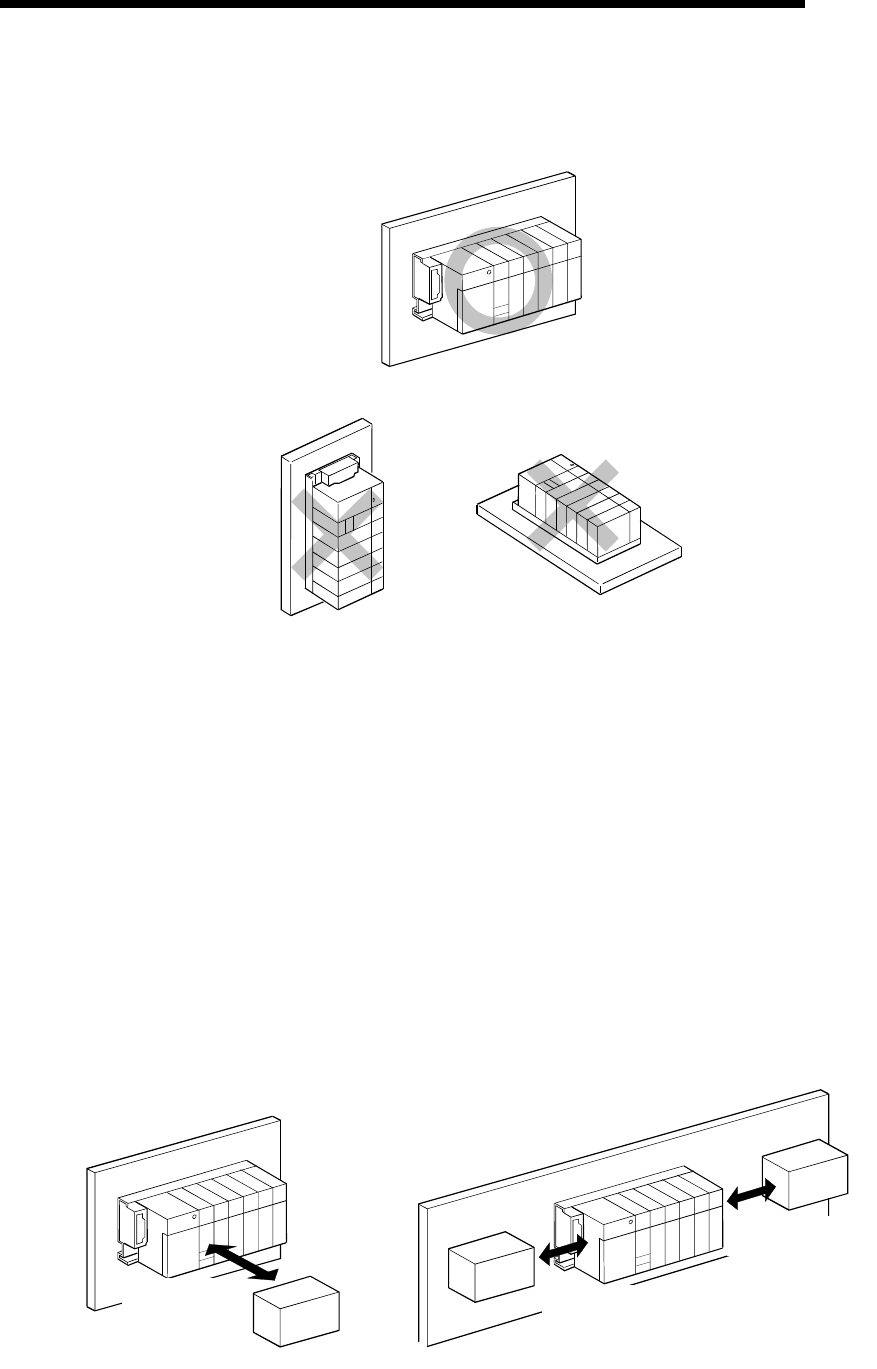
9 - 14 9 - 14
MELSEC-Q
9 LOADING AND INSTALLATION
(2) Module mounting orientation
(a) Since the PLC generates heat, it should be mounted on a well ventilated
location in the orientation shown below.
(b) Do not mount it in either of the orientations shown below.
Vertical Flat
(3) Installation surface
Mount the base unit on a flat surface. If the mounting surface is not even, this
may strain the printed circuit boards and cause malfunctions.
(4) Installation of unit in an area where the other devices are installed
Avoid mounting base unit in proximity to vibration sources such as large
magnetic contractors and no-fuse circuit breakers; mount these on a separate
panel or at a distance.
(5) Distances from the other devices
In order to avoid the effects of radiated noise and heat, provide the clearances
indicated below between the PLC and devices that generate noise or heat
(contactors and relays).
• Required clearance in front of PLC : at least 100 mm (3.94 inch)
• Required clearance on the right and left of PLC : at least 50 mm (1.97 inch)
Contactor, relay, etc.
At least 100mm
(3.94 inch) At least 50mm
(1.97 inch)
At least 50mm
(1.97 inch)
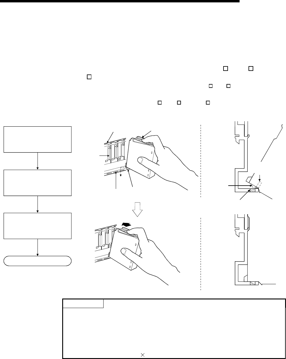
9 - 15 9 - 15
MELSEC-Q
9 LOADING AND INSTALLATION
9.3.3 Installation and removal of module
This section explains how to install and remove a power supply, CPU, I/O, intelligent
function or another module to and from the base unit.
(1) Installation and removal of the module from Q3 B, ,Q5 B and
Q6 B
The installation and removal of the module from Q3 B/Q6 B base unit are
described below.
(a) Installation of module on Q3 B, Q5 B and Q6 B
Module
Module fixing latch
Module fixing
hole
Module
connector
Base unit
Base unit
Module loading
lever
Module
fixing latch
Module fixing hole
Insert the module fixing latch
into the module fixing hole of
the base unit.
Push the module in the
direction of arrow to load it
into the base unit.
Make sure that the module
is inserted in the base unit
securely.
Completion
POINTS
(1) Always insert the module fixing latch of the module into the module fixing hole.
Forcing the hook into the hole will damage the module connector and module.
(2) When using the PLC in a place where there is large vibration or impact, screw
the CPU module to the base unit.
Module fixing screw : M3 12 (user-prepared)
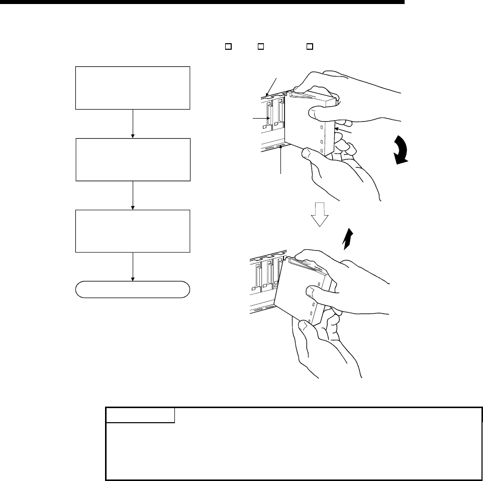
9 - 16 9 - 16
MELSEC-Q
9 LOADING AND INSTALLATION
(b) Removal from Q3 B, Q5 B and Q6 B
Module
connector Module
Module fixing hole
Base unit
Completion
Hold the module with both
hands, and push the unit fixing
hook on the top of the module
with a finger until it stops.
While pushing the unit fixing
hook, and using the bottom of
the module as a support, pull
the module toward you.
Lift the module upwards and
remove the module fixing
latch from the module
fixing hole.
POINT
When the module fixing screw is used, always remove the module by removing the
module fixing screw and then taking the module fixing latch off the module fixing
hole of the base unit.
Do not try to remove the module forcibly since this may damage the module.
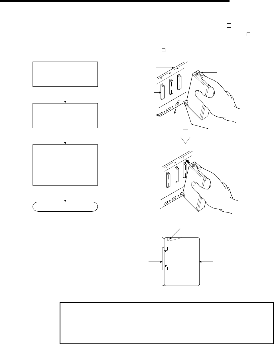
9 - 17 9 - 17
MELSEC-Q
9 LOADING AND INSTALLATION
(2) Installation and removal of the module from QA1S6 B
The procedure for installing and removing the module from the QA1S6 B base
unit is described below.
(a) Installation of module on QA1S6 B
Insert the module fixing
projections into the module
fixing hole in the base unit.
Install the module onto the
base unit by pushing the
top forward.
Make sure that the module is
firmly inserted in the base
unit.
Then, secure it with
the module mounting screw.
Completion
Base unit
Module
connector
Module
fixing hole
Module
Module fixing
projections
Base unit
Module mounting screw
Module
POINT
Make sure to install the module, with the module fixing projection inserted into the
module fixing hole, using the module fixing screws.
Do not try to forcibly install the module without inserting the projection into the hole,
since this may damage the module connector and the module.
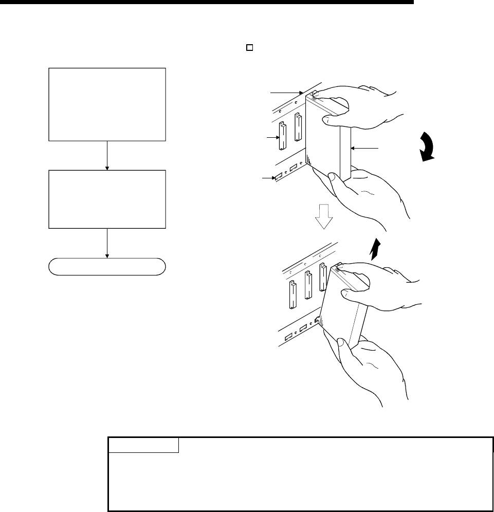
9 - 18 9 - 18
MELSEC-Q
9 LOADING AND INSTALLATION
(b) Removal from QA1S6 B
Remove the module mounting
screw, and using the bottom
of the module as a support,
pull the top of the module
toward you.
Lift the module upwards and
remove the module fixing
projections from the module
fixing hole.
Completion
Base unit
Module
connector
Module
fixing hole
Module
POINT
To remove the module, make sure to remove the module fixing screws, and then
disengage the module fixing projection from the module fixing hole.
Do not try to remove the module forcibly since this may damage the module fixing
projection.
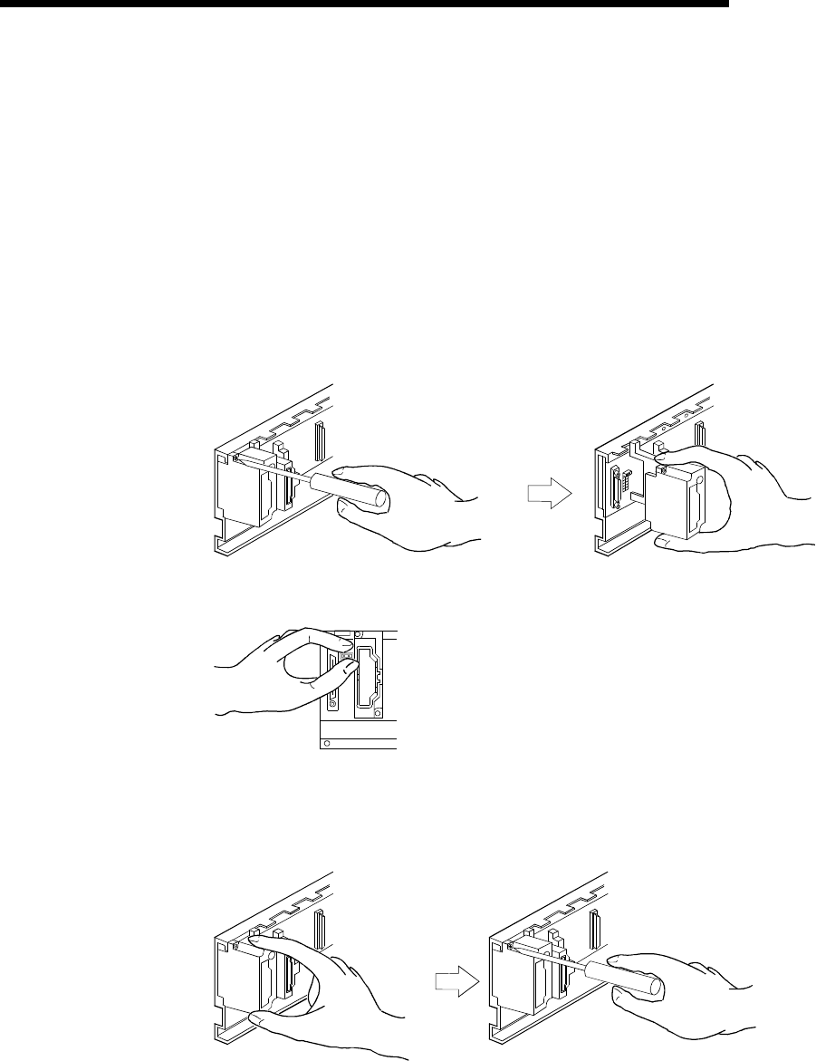
9 - 19 9 - 19
MELSEC-Q
9 LOADING AND INSTALLATION
9.4 How to Set Stage Numbers for the Extension Base Unit
When using two or more extension base units, their stage numbers must be set with
their stage number setting connectors. Extension 1 need not be set since the
extension number is factory-set to 1.
Make this setting in the following procedure.
(1) The stage number setting connector of the extension base unit is located under the
IN side base cover. (Refer to Section 6.4 for the setting of the extension number
setting connector.)
First, loosen the upper and lower screws in the IN side base cover and remove the
base cover from the extension base unit.
(2) Insert the connector pin in the required stage number location of the connector
(PIN1) existing between the IN and OUT sides of the extension cable connector.
OUT
(3) Install the base cover to the extension base unit and tighten the base cover screw.
(Tightening torque: 36 to 48N • cm)
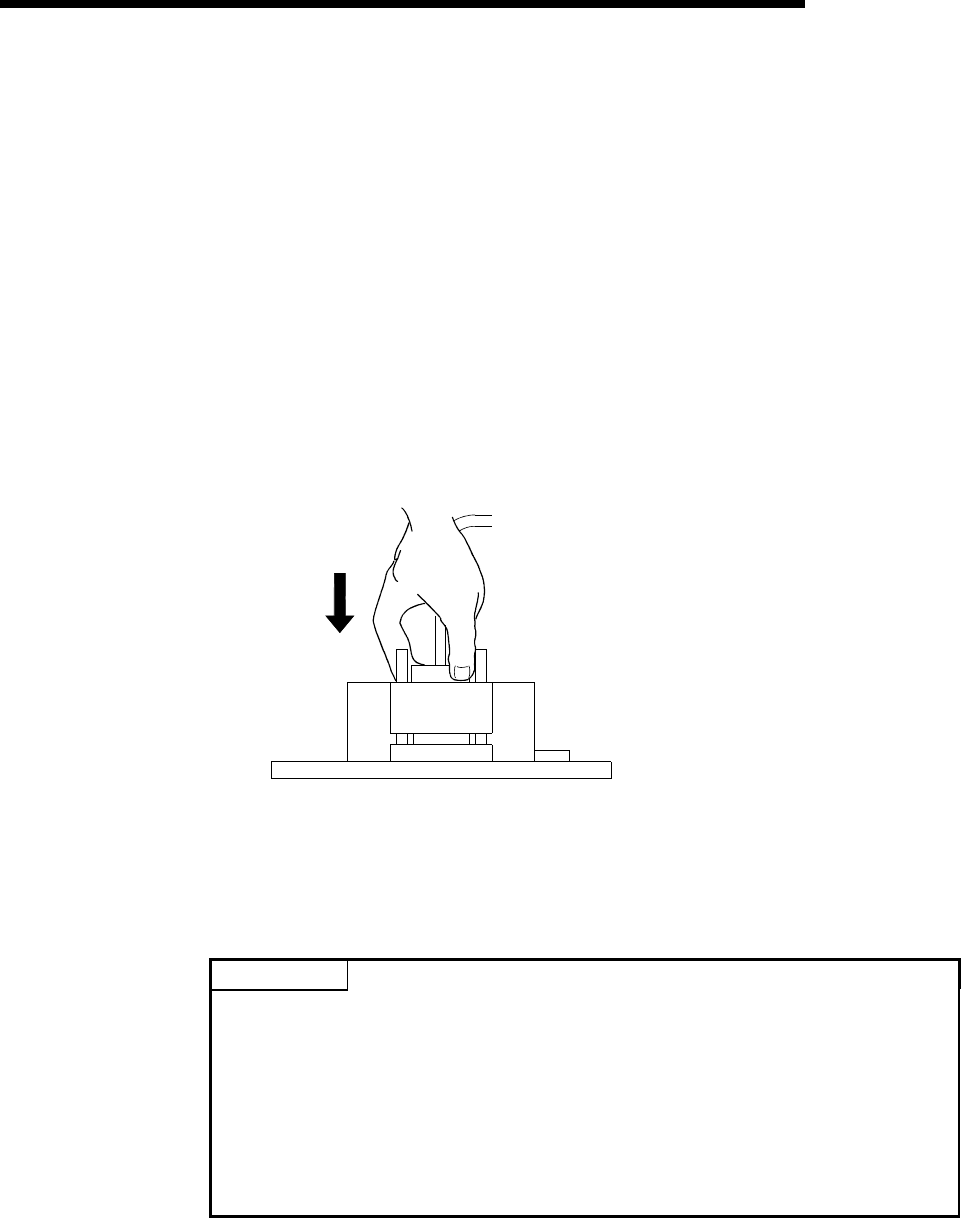
9 - 20 9 - 20
MELSEC-Q
9 LOADING AND INSTALLATION
9.5 Connection and Disconnection of Extension Cable
(1) Instructions for handling an extension cable
• Do not stamp an extension cable.
• An extension cable must be connected to the base unit when the base cover
has been installed.
(After you have set the extension number to the extension base unit, reinstall
and screw the base cover.)
• When running an extension cable, the minimum bending radius of the cable
should be 55mm (2.17 inch) or more.
If it is less than 55mm (2.17 inch), a malfunction may occur due to characteristic
deterioration, open cable or the like.
• When connecting or disconnecting an extension cable, do not hold the ferrite
cores mounted at both ends of the cable.
Hold the connector part of the cable for connection or disconnection.
Holding the ferrite core may cause the cable to open within the connector.
Also, if the ferrite core is shifted, the characteristic will change. When handling
the cable, take care not to shift the ferrite core positions.
(2) Connection of extension cable
POINT
When connecting an extension base unit to the main base unit with an extension
cable, always plug the OUT side connector of the main base unit and the IN side
connector of the extension base unit with an extension cable. The system will not
operate properly if the extension cable is connected in the form of IN to IN, OUT to
OUT or IN to OUT.
When connecting two or more extension base units, plug the OUT side connector
of the first extension base unit and the IN side connector of the second extension
base unit with an extension cable.
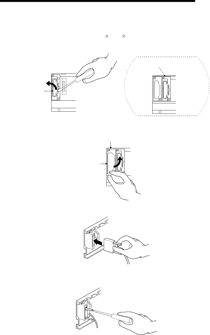
9 - 21 9 - 21
MELSEC-Q
9 LOADING AND INSTALLATION
(a) To connect an extension cable to the main base unit, remove the portion
under the OUT characters on the base cover with a tool such as a flat-blade
screwdriver (5.5 75, 6 100).
This also applies to a case where an extension cable is connected to the OUT
side connector of the extension base unit.
Base cover
OUT
Main base unit
OUTIN
OUT side of extension
base unit
(b) To connect the extension cable to the next extension base unit, remove the
seal applied under the IN characters on the base cover.
S
eal
OUTIN
IN side of extension
base unit
(c) When plugging the extension cable to any base unit, hold the connector part
of the extension cable.
(d) After fitting the extension cable, always tighten the extension cable connector
fixing screws.
(Tightening torque: 20N • cm)

9 - 22 9 - 22
MELSEC-Q
9 LOADING AND INSTALLATION
(3) Disconnection of extension cable
When unplugging the extension cable, hold and pull the connector part of the
extension cable after making sure that the fixing screws have been removed
completely.
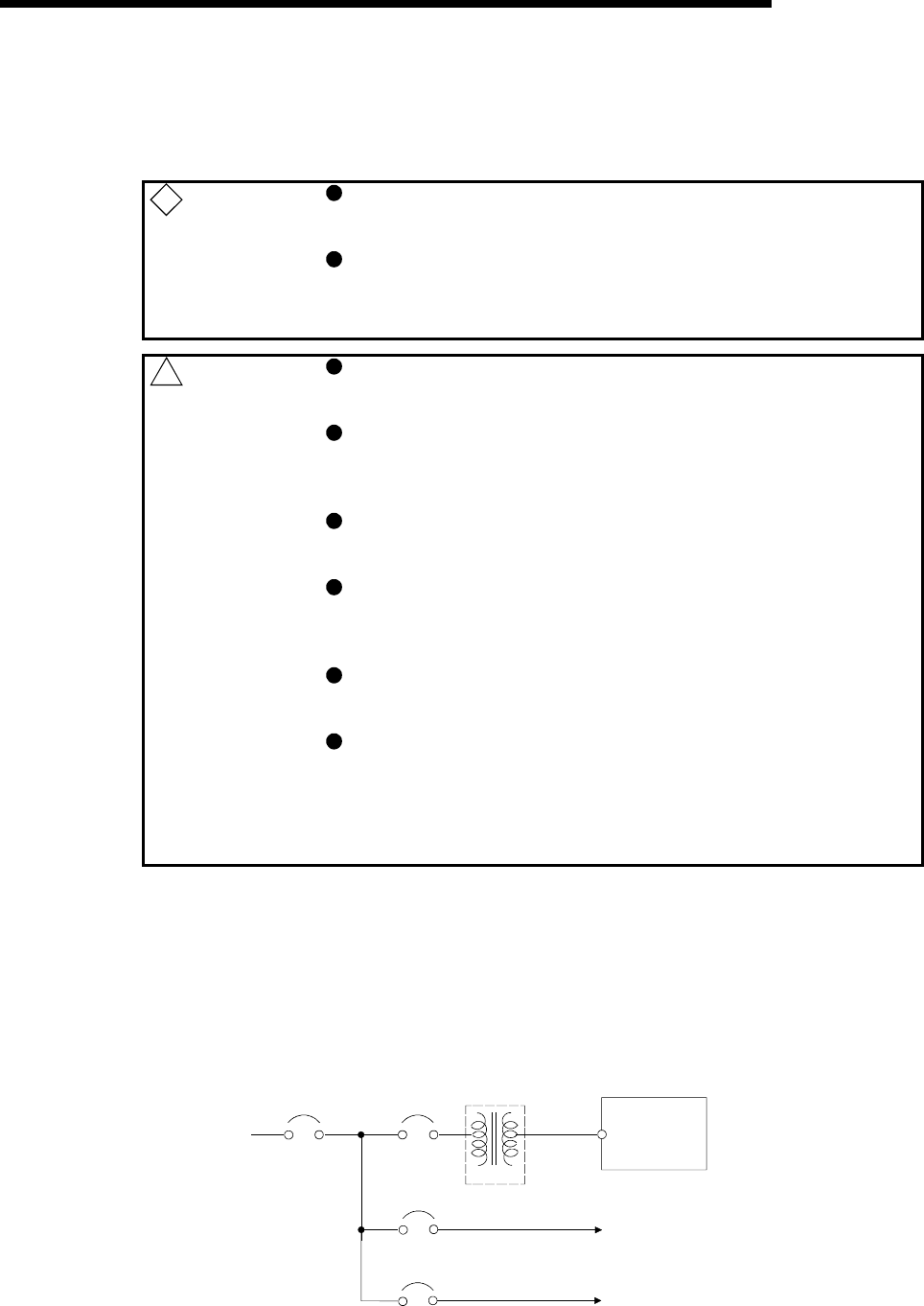
9 - 23 9 - 23
MELSEC-Q
9 LOADING AND INSTALLATION
9.6 Wiring
9.6.1 The precautions on the wiring
! DANGER Completely turn off the external power supply when installing or
placing wiring. Not completely turning off all power could result in
electric shock or damage to the product.
When turning on the power supply or operating the module after
installation or wiring work, be sure that the module's terminal covers are
correctly attached. Not attaching the terminal cover could result in
electric shock.
! CAUTION Be sure to ground the FG terminals and LG terminals to the
protective ground conductor. Not doing so could result in electric
shock or erroneous operation.
When wiring in the PLC, be sure that it is done correctly by checking
the product's rated voltage and the terminal layout. Connecting a
power supply that is different from the rating or incorrectly wiring the
product could result in fire or damage.
External connections shall be crimped or pressure welded with the
specified tools, or correctly soldered. Imperfect connections could
result in short circuit, fires, or erroneous operation.
Tighten the terminal screws with the specified torque. If the terminal screws
are loose, it could result in short circuits, fire, or erroneous operation.
Tightening the terminal screws too far may cause damages to the screws
and/or the module, resulting in fallout, short circuits, or malfunction.
Be sure there are no foreign substances such as sawdust or wiring
debris inside the module. Such debris could cause fires, damage, or
erroneous operation.
The module has an ingress prevention label on its top to prevent
foreign matter, such as wire offcuts, from entering the module during
wiring.
Do not peel this label during wiring.
Before starting system operation, be sure to peel this label because
of heat dissipation.
The precautions on the connection of the power cables are described below.
(1) Power supply wiring
(a) Separate the PLC's power supply line from the lines for I/O devices and
power devices as shown below.
When there is much noise, connect an insulation transformer.
PLC
PLC power
supply
Main power
supply
I/O power supply
Main circuit device
I/O devices
Main circuit devic
e
Insulation
transformer
2
00VAC
T1
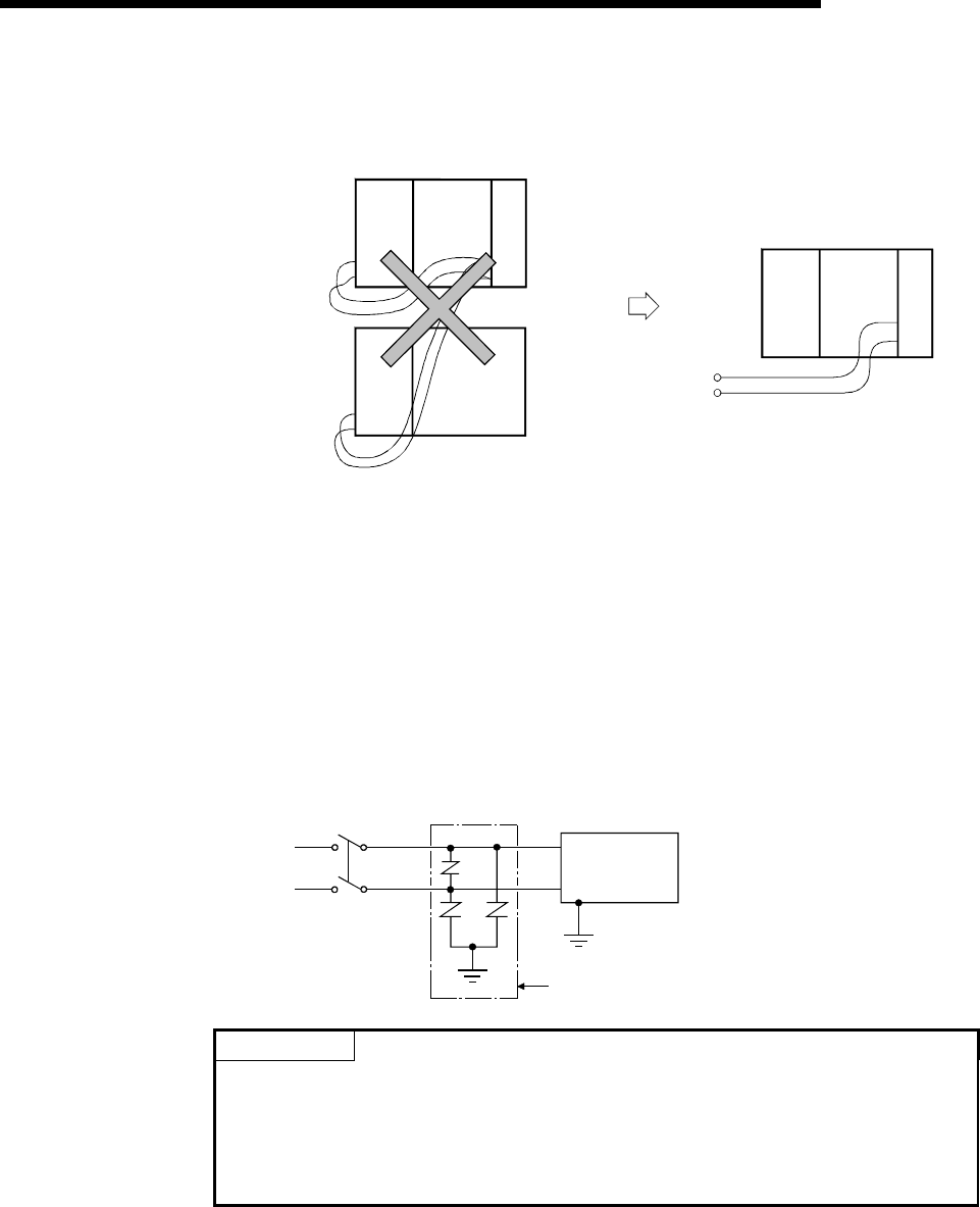
9 - 24 9 - 24
MELSEC-Q
9 LOADING AND INSTALLATION
(b) Do not connect the 24VDC outputs of two or more power supply modules in
parallel to supply power to one I/O module. Parallel connection will damage
the power supply modules.
24VDC
24VDC 24VDC
Power supply
module
Power supply
module
I/O module
I/O module
Power supply
module
External power supply
(c) 100VAC, 200VAC and 24VDC wires should be twisted as dense as possible.
Connect the modules with the shortest distance.
Also, to reduce the voltage drop to the minimum, use the thickest wires
possible (maximum 2mm2).
(d) Do not bundle the 100VAC and 24VDC wires with, or run them close to, the
main circuit (high voltage, large current) and I/O signal lines. Reserve a
distance of at least 100 mm from adjacent wires.
(e) As a countermeasure to power surge due to lightening, connect a surge
absorber for lightening as shown below.
AC
E1
E2
Surge absorber for lightening
PLC
POINT
(1) Separate the ground of the surge absorber for lightening (E1) from that of the
PLC (E2).
(2) Select a surge absorber for lightening whose power supply voltage does no
exceed the maximum allowable circuit voltage even at the time of maximum
power supply voltage elevation.
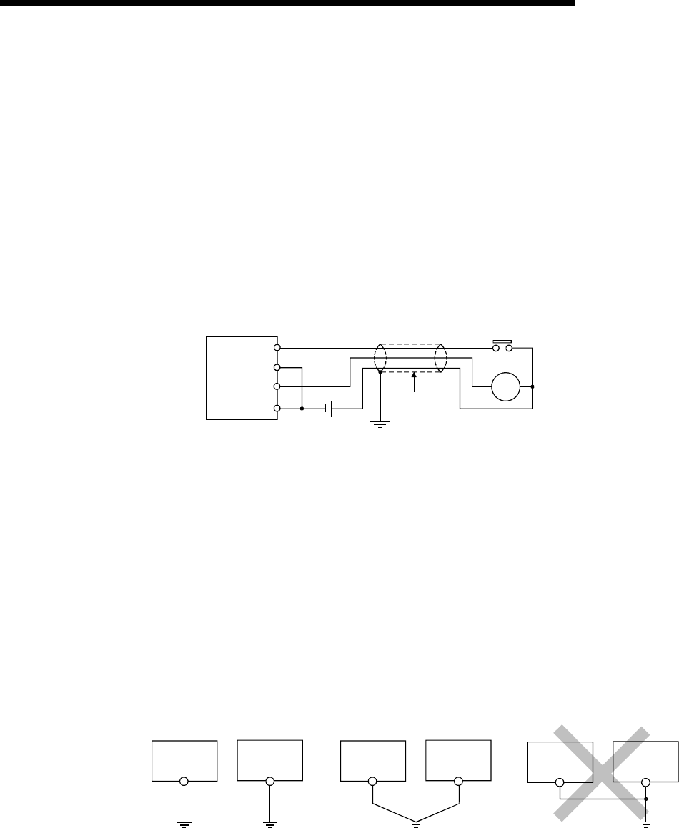
9 - 25 9 - 25
MELSEC-Q
9 LOADING AND INSTALLATION
(2) Wiring of I/O equipment
(a) Insulation-sleeved crimping terminals cannot be used with the terminal block.
It is recommended to cover the wire connections of the crimping terminals
with mark or insulation tubes.
(b) The wires used for connection to the terminal block should be 0.3 to 0.75mm2
in core and 2.8mm (0.11 inch) max. in outside diameter.
(c) Run the input and output lines away from each other.
(d) When the wiring cannot be run away from the main circuit and power lines,
use a batch-shielded cable and ground it on the PLC side.
In some cases, ground it in the opposite side.
Input
Output
PLC Shielded cable
Shield
DC
RA
(e) Where wiring runs through piping, ground the piping without fail.
(f) Run the 24VDC input line away from the 100VAC and 200VAC lines.
(g) Wiring of 200m (686.67 ft.) or longer distance will give rise to leakage currents
due to the line capacity, resulting in a fault.
Refer to Section 11.5 for details.
(3) Grounding
To ground the cable, follow the steps (a) to (c) shown below.
(a) Use the dedicated grounding as far as possible.
(b) When a dedicated grounding cannot be performed, use (2) Common
Grounding shown below.
PLC Another
equipment
grounding
(1) Independent grounding.....Best (2) Common grounding.....Good (3) Joint grounding.....Not allowe
d
PLC Another
equipment
PLC Another
equipment
grounding
(c) For grounding a cable, use the cable of 2 mm2 or more.
Position the ground-contact point as closely to the sequencer as possible, and
reduce the length of the grounding cable as much as possible.
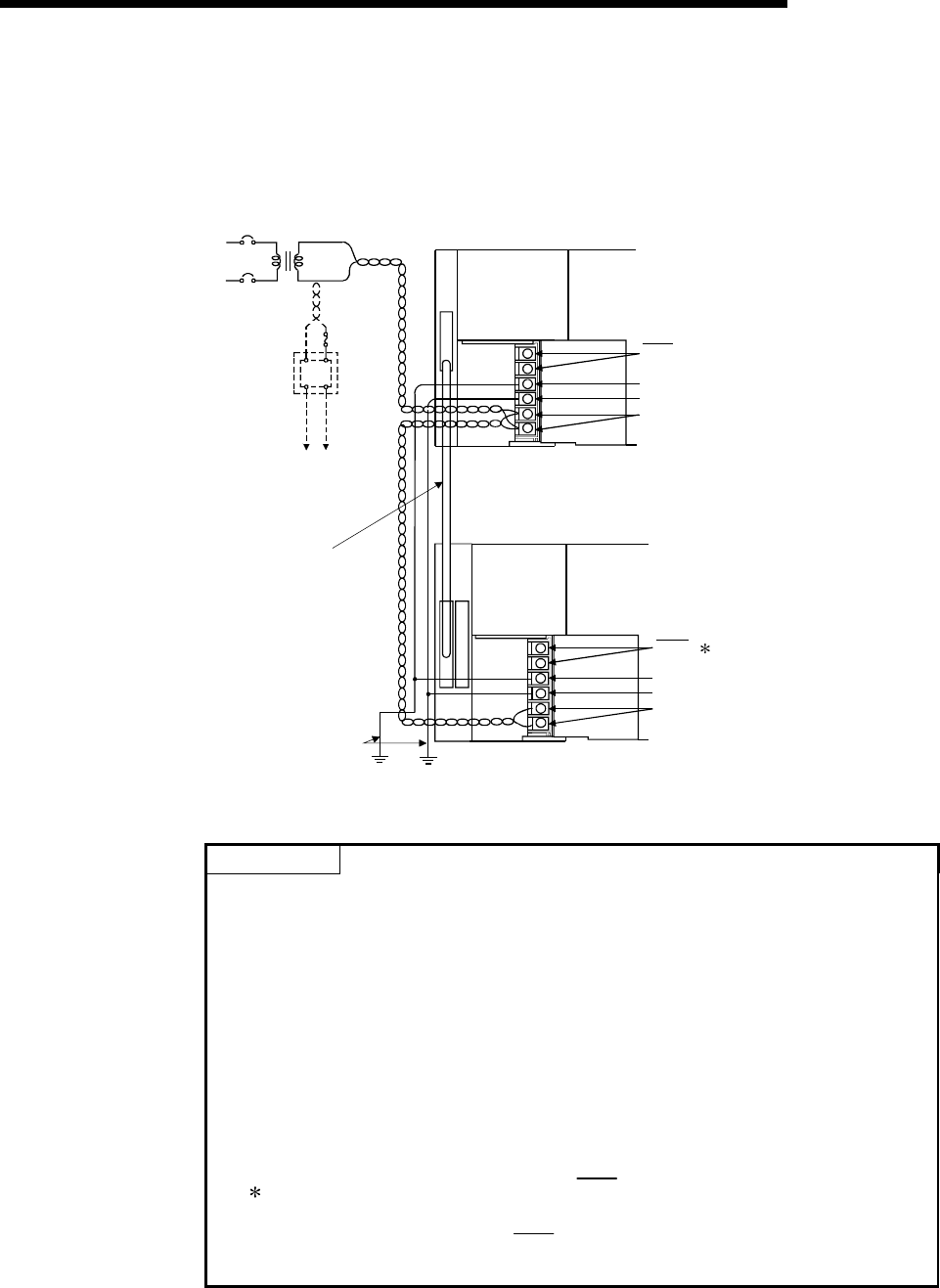
9 - 26 9 - 26
MELSEC-Q
9 LOADING AND INSTALLATION
9.6.2 Connecting to the power supply module
The following diagram shows the wiring example of power lines, grounding lines, etc.
to the main and extension base units.
AC
100/110VAC
Fuse
24VDC
AC
DC
Connect to 24VDC terminals
of I/O module that
requires 24VDC internally.
Extension cable
Ground wire
Grounding
Main base unit
(Q38B)
Q61P-A1 CPU module
Extension base unit
(Q68B)
Q61P-A1 I/O
100VAC
ERR
FG
LG
INPUT
100-120VAC
FG
LG
INPUT
100-120VAC
ERR 1
POINTS
(1) Use the thickest possible (max. 2 mm2 (14 AWG)) wires for the 100/200 VAC
and 24 VDC power cables. Be sure to twist these wires starting at the
connection terminals. To prevent a short-circuit should any screws loosen, use
solderless terminals with insulation sleeves.
(2) When the LG terminals and FG terminals are connected, be sure to ground the
wires. Do not connect the LG terminals and FG terminals to anything other than
ground. If LG terminals and FG terminals are connected without grounding the
wires, the PLC may be susceptible to noise.
In addition, since the LG terminals have potential, the operator may receive an
electric shock when touching metal parts.
(3) 1 An error cannot be output from the ERR terminal of the power supply
module loaded on the extension base.
To output an error, use the ERR terminal of the power supply module
loaded on the main base unit.
10 - 1 10 - 1
MELSEC-Q
10 MAINTENANCE AND INSPECTION
10 MAINTENANCE AND INSPECTION
! DANGER Do not touch the terminals while power is on.
Doing so could cause shock.
Correctly connect the battery. Also, do not charge, disassemble,
heat, place in fire, short circuit, or solder the battery.
Mishandling of a battery can cause overheating or cracks which
could result in injury and fires.
Turn the power off when cleaning the module or tightening the
terminal screws or module mounting screws.
Conducting these operations when the power is on could result in
electric shock.
Loose terminal screws may cause short circuits or malfunctions.
Failure to mount the module properly will result in short circuit,
malfunction or in the module falling.
! CAUTION In order to ensure safe operation, read the manual carefully to
acquaint yourself with procedures for program change, forced
outputs, RUN, STOP, and PAUSE operations, etc., while operation
is in progress.
Operation mistakes could cause damage to the equipment and
other problems.
Never try to disassemble of modify module. It may cause product
failure, malfunction, fire or cause injury.
When using any radio communication device such as a cellular
phone or a PHS phone, keep them away from the controller at least
25 cm (9.85 inch) or it may cause a malfunction.
Turn the power off when installing or removing the modules.
Trying to install or remove the module while the power is on could
damage the module or result in erroneous operation.
In order that you can use the PLC in normal and optimal condition at all times, this
section describes those items that must be maintained or inspected daily or at regular
intervals.
10

10 - 2 10 - 2
MELSEC-Q
10 MAINTENANCE AND INSPECTION
10.1 Daily Inspection
The items that must be inspected daily are listed below.
Daily inspection
Item Inspection Item Inspection Judgment Criteria Remedy
1 Installation of base unit Check that fixing screws
are not loose and the
cover is not dislocated.
The screws and cover must be installed
securely. Further tighten the
screws.
2 Installation of I/O
module
Check that the module is
not dislocated and the unit
fixing hook is engaged
securely.
The unit fixing hook must be engaged and
installed securely. Securely engaged
the unit fixing hook.
Check for loose terminal
screws. Screws should not be loose. Retighten terminal
screws
Check distance between
Solderless terminals. The proper clearance should be provided
between Solderless terminals Correct.
3 Connecting conditions
Check connectors of
extension cable. Connections should no be loose. Retighten connector
mounting screws.
Power supply
"POWER" LED Check that the LED is ON. The LED must be ON. (Abnormal if the
LED is OFF.)
CPU
"RUN" LED Check that the LED is ON
in RUN status. The LED must be ON. (Abnormal if the
LED is OFF.)
CPU
"ERR." LED Check that the LED is
OFF. The LED must be OFF. (Abnormal if the
LED is ON or flickering.)
CPU
"BAT." LED Check that the LED is
OFF. The LED must be OFF. (Abnormal if the
LED is ON.)
Input LED Check that the LED turns
ON and OFF.
The LED must be ON when the input
power is turned ON.
The LED must be extinguished when the
input power is turned OFF.
(Abnormal if the LED does not turn ON or
turn OFF as indicated above.)
4
Module indication LED
Output LED Check that the LED turns
ON and OFF.
The LED turns ON when the output power
is turned ON.
The LED must be extinguished when the
output power is turned OFF.
(Abnormal if the LED does not turn ON or
turn OFF as indicated above.)
Follow Section 10.2.
10
10 - 3 10 - 3
MELSEC-Q
10 MAINTENANCE AND INSPECTION
10.2 Periodic Inspection
The items that must be inspected one or two times every 6 months to 1 year are listed
below.
When the equipment is moved or modified, or layout of the wiring is changed, also
perform this inspection.
Periodic Inspection
Item Inspection Item Inspection Judgment Criteria Remedy
Ambient
temperature 0 to 55 °C
Ambient humidity 5 to 95 %RH 1
1
Ambient environment
Atmosphere
Measure with a thermometer
and a hygrometer.
Measure corrosive gas.
Corrosive gas must not be
present.
When the sequencer is
used in the board, the
ambient temperature in
the board becomes the
ambient temperature.
85 to 132VAC
170 to 264VAC
2 Power voltage Measure a voltage across the
terminals of 100/200VAC and
24VDC. 15.6 to 31.2VDC
Change the power
supply.
Looseness, rattling Move the module to check for
looseness and rattling. The module must be installed
fixedly.
Further tighten screws.
If the CPU, I/O, or power
supply module is loose,
fix it with screws.
3
Installation
Adhesion of dirt and
foreign matter Check visually. Dirt and foreign matter must
not be present. Remove and clean.
Looseness of
terminal screws Try to further tighten screws
with a screwdriver. Screws must not be loose. Further tighten.
Proximity of
solderless terminals
to each other Check visually. Solderless terminals must be
positioned at proper intervals. Correct.
4
Connection
Looseness of
connectors Check visually. Connectors must not be loose. Further tighten connector
fixing screws.
5 Battery check on the monitor mode of
the GX Developer that SM51 or
SM52 is turned OFF. (Preventive maintenance)
Even if the lowering of a
battery capacity is not
shown, replace the
battery with a new one if
a specified service life of
the battery is exceeded.
1 When AnS Series Module is included in the system, the judgement criteria will be from 10 to 90 % RH.
10 - 4 10 - 4
MELSEC-Q
10 MAINTENANCE AND INSPECTION
10.3 Battery Replacement
When the voltage of the program and power interrupt hold-on function backup battery
is lowered, the special relays SM51 and SM52 are energized.
Even if these special relays are energized, the contents of the program and power
interrupt hold-on function are not erased immediately.
If the energization of these relays is recognized, however, these contents may be
deleted unintentionally.
While a total of the power interrupt hold-on time after the SM51 is energized is within a
specified time, replace the battery with a new one.
POINTS
The SM51 is used to give an alarm when the capacity of the battery is lowered.
Even after it is energized, the data is held for a specified time.
For safety, however, replace the battery with a new one as early as possible.
The SM52 is energized when the battery causes a complete discharge error.
Immediately after the relay has been energized, replace the battery with a new one.
Whichever voltage of the battery of the CPU module and SRAM card is lowered, the
SM51 and SM52 are energized.
To identify the specific battery of the memory of which voltage is lowered, check the
contents of the special resisters SD51 and SD52.
When the voltage of the battery of each memory is lowered, the bit corresponding to
each of SD51 and SD52 memories is turned on.
Bit No. of SD51 and SD52 Object
Bit 0 CPU module
Bit 1, 2 SRAM card
POINTS
The relation between the backups of the memories preformed by the batteries
which are installed on the CPU module and SRAM card is described below.
The items that must be considered are the following two points.
1) The battery installed on the CPU module cannot backup the memory of the
SRAM card.
2) The battery installed on the SRAM card cannot backup the memory of the CPU
module.
Power supply
Module Battery of CPU
Module Battery of
SRAM Card Memory of CPU
Module Memory of
SRAM Card
ON
Connection OFF
ON
ON
Unconnection OFF
ON
Connection OFF
ON
OFF Unconnection OFF
: Backup enable : Backup unable
The standard service life and replacement procedures of the battery is described on
the next page.
10 - 5 10 - 5
MELSEC-Q
10 MAINTENANCE AND INSPECTION
10.3.1 Battery life
(1) CPU module battery (Q6BAT) life
(a) The CPU module battery life is given below.
Battery life
CPU Module
Type
Energization
Time Ratio
1 Guaranteed value
(MIN)
Value in actual use
(TYP)
After SM51 is energized
(Guaranteed time after
alarm occurrence)
0% 5433hr 13120hr 120hr
30% 7761hr 18742hr 120hr
50% 10866hr 26240hr 120hr
70% 18110hr 43733hr 120hr
Q02CPU
100% 10years 10years 120hr
0% 2341hr 6435hr 120hr
30% 3344hr 9192hr 120hr
50% 4682hr 12870hr 120hr
70% 7803hr 21450hr 120hr
Q02HCPU
Q06HCPU
100% 10years 10years 120hr
0% 1260hr 4228hr 48hr
30% 1800hr 6040hr 48hr
50% 2520hr 8456hr 48hr
70% 4200hr 14093hr 48hr
Q12HCPU
Q25HCPU
100% 10years 10years 48hr
1: The energization time ratio denotes the ratio of power-on time in a day (24 hours).
(When power is on for 12 hours and off for 12 hours, the energization time ratio is
50%.)
(b) The Q6BAT life is 10 years when it is used without connecting to the CPU
module.
(2) SRAM card battery life
The SRAM card battery life changes depending on the combination of the serial
number (first 5 digits) of the CPU module and the manufacturing control number
of the memory card.
The SRAM card battery life is indicated below.
(a) CPU module whose serial number's first 5 digits are "04012" or later
Battery life
SRAM card
Energization
Time Ratio
1 Guaranteed value
(MIN)
Value in actual use
(TYP)
After SM51 is energized
(Guaranteed time after
alarm occurrence)
0% 690hr 6336hr 8hr
Q2MEM-1MBS
Manufacturing
control number
"A" 2 100% 11784hr 13872hr 8hr
0% 2400hr 2.7years 20hr
30% 2880hr 3.6years 20hr
50% 4320hr 4.5years 20hr
70% 6480hr 5.0years 20hr
Q2MEM-1MBS
Manufacturing
control number
"B" 2 100% 5.0years 5.0years 50hr
0% 2400hr 2.7years 20hr
30% 2880hr 3.6years 20hr
50% 4320hr 4.5years 20hr
70% 6480hr 5.0years 20hr
Q2MEM-2MBS
100% 5.0years 5.0years 50hr
10 - 6 10 - 6
MELSEC-Q
10 MAINTENANCE AND INSPECTION
(b) CPU module whose serial number's first 5 digits are "04011" or earlier
Battery life
SRAM card
Energization
Time Ratio
1
Guaranteed value
(MIN)
Value in actual use
(TYP)
After SM51 is energized
(Guaranteed time after
alarm occurrence)
0% 690hr 6336hr 8hr
Q2MEM-1MBS
Manufacturing
control number
"A"
2
Q2MEM-2MBS
100% 11784hr 13872hr 8hr
1: The energization time ratio denotes the ratio of power-on time in a day (24 hours) .
(When power is on for 12 hours and off for 12 hours, the energization time ratio is
50%.)
2: The manufacturing control number is given on the SRAM card rear label (see
below).
CAUTION
Do not subject to mechanical shock!
Do not expose to extreme temperrature,
Manufacturing control number
POINT
Remember that the SRAM card consumes battery power even when the battery is
connected to the CPU module and the power is turned ON.
If the special relay SM51 (battery low latch) turns on, immediately replace the battery.
If an alarm has not yet occurred, it is recommended to replace the battery periodically
according to the conditions of use.
10 - 7 10 - 7
MELSEC-Q
10 MAINTENANCE AND INSPECTION
10.3.2 Battery replacement procedure
(1) CPU module battery replacement procedure
When the CPU module battery has been exhausted, replace the battery with a
new one according to the procedure shown below. The PLC power must be on
for 10 minutes or longer before dismounting the battery.
Even when the battery is dismounted, the memories are backed up by the
capacitor for a while. However, if the replacement time exceeds the guaranteed
value specified in the table below, the contents stored in the memories may be
erased. To prevent this trouble, replace the battery speedily.
Backup time by capacitor
Backup time by capacitor[min]
3
Front
Side of the CPU module
Remove the old battery from
its holder.
Insert a new battery into the holder in
the correct direction.
Connect the lead to the connector.
Completion
Close the cover of the CPU module.
Monitor
SM51 to verify on/off.
Monitor
SD52 to verify the bit number
that is on.
The CPU module battery is faulty.
The memory card battery is faulty.
Refer to Section 10.3.2 (2).
Bits other than 0 are on.
Bit 0 is on.
ON
OFF
Open the cover of the CPU module.
Replacing battery
Remove the CPU module from the
base unit.
Turn off the PLC power supply.
.
Install the CPU module into the
base unit.
Turn on the PLC power supply.
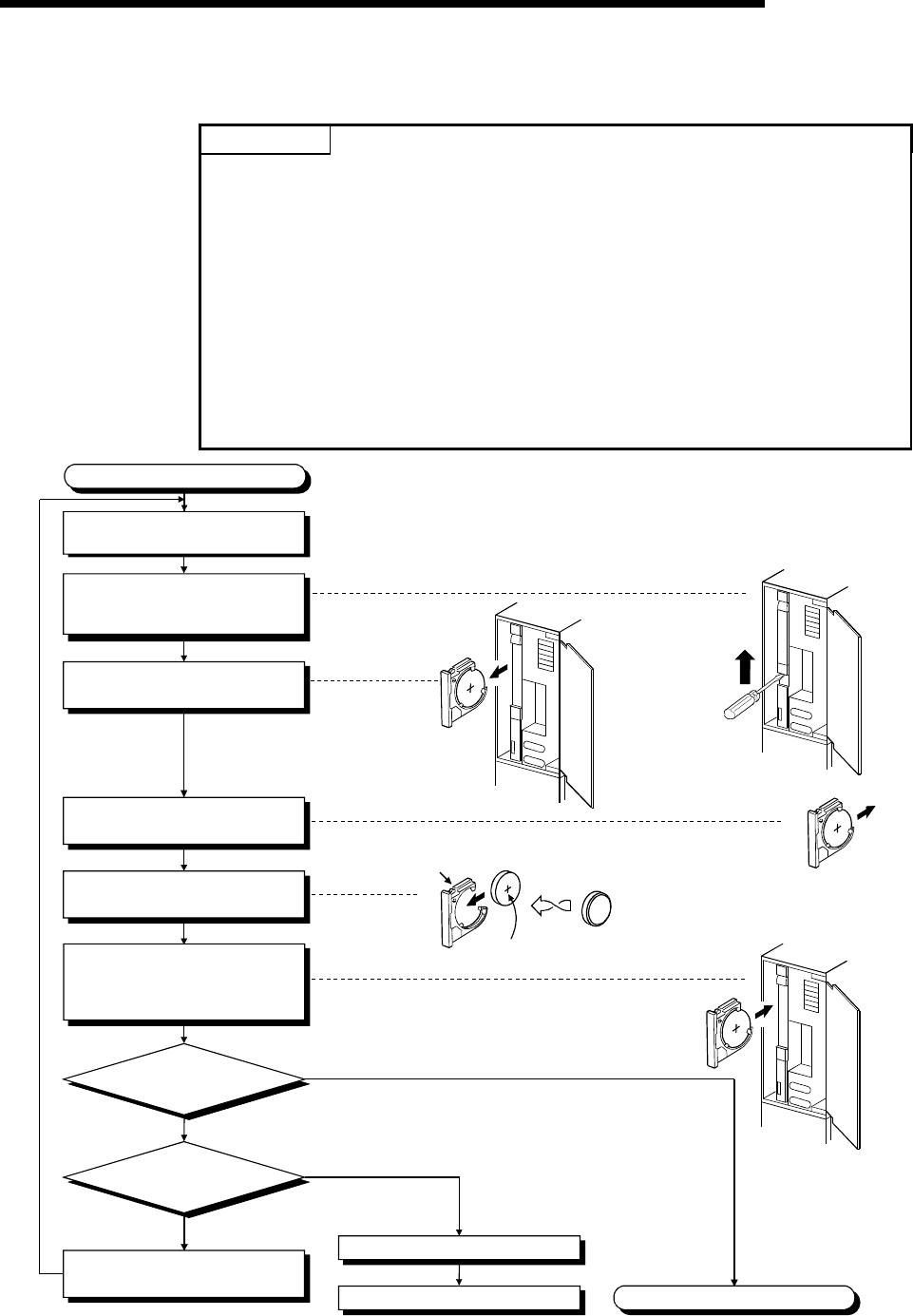
10 - 8 10 - 8
MELSEC-Q
10 MAINTENANCE AND INSPECTION
(2) SRAM card CPU module battery replacement procedure
Replace the SRAM card battery in the following procedure.
POINTS
Replace the battery while paying attention to the following.
(a) To back up the data, replace the SRAM card battery with the PLC power supply
ON and the SRAM card installed.
(b) Start replacement after backing up the CPU module data using GX Developer.
(c) Since replacement is made with the PLC power supply ON, take extreme care
not to get an electric shock.
(d) When dismounting or mounting the battery holder on the SRAM card, take care
so that the battery does not come out of the battery holder.
(e) When replacing the battery with the PLC power supply OFF, always back up the
data before starting replacement.
[Battery replacement procedure]
1) Back up the SRAM card data using GX Developer.
2) Replace the battery.
3) Write the backed up data from GX Developer to the memory card.
Completion
Monitor
SM52 to verify on/off.
Monitor
SD52 to verify the bit number
that is on.
The CPU module battery is faulty.
Refer to Section 10.3.2 (1).
Bit 0 is on.
A bit other than 0 is on
ON
OFF
Replacing battery
Using a flat screw-driver, slide the
battery holder's locking switch
away from the "LOCK" position.
Remove the battery holder from
the SRAM card.
Remove the old battery from
its holder.
Insert a new battery into the holder
in the correct direction.
Push the battery holder all the way
into the memory card, and confirm
that the battery holder's locking
switch is set to the "LOCK" position.
"RELEASE"
position
'+' sign
Open the front cover while the
PLC power supply is on.
Bit 1 or 2 on:
Memory card A battery is faulty.
Battery holder

11 - 1 11 - 1
MELSEC-Q
11 TROUBLESHOOTING
11 TROUBLESHOOTING
This section describes the various types of trouble that occur when the system is
operated, and causes and remedies of these troubles.
11.1 Troubleshooting Basics
In order to increase the reliability of the system, not only highly reliable devices are
used but also the speedy startup of the system after the occurrence of trouble
becomes an important factor.
To start up the system speedily, the cause of the trouble must be located and
eliminated correctly.
The basic three points that must be followed in the troubleshooting are as follows.
(1) Visual inspection
Visually check the following.
1) Movement of sequencer (stopped condition, operating condition)
2) Power supply on/off
3) Status of input/output devices
4) Power supply module, CPU module, I/O module, intelligent function module,
installation condition of extension cable
5) Status of wiring (I/O cables, cables)
6) Display status of various types of indicators ("POWER" LED, "RUN" LED,
"ERR." LED, I/O LED)
7) Status of setting of various types of set switches (Setting of No. of stages of
extension base unit, power interrupt hold-on status)
After confirming items 1) to 7), connect the GX Developer, and check the
operating conditions of the PLC and the contents of the program.
(2) Check of trouble
Check to see how the operating condition of the PLC varies while the PLC is
operated as follows.
1) Set the RUN/STOP switch to STOP.
2) Reset the trouble with the RESET/L.CLR switch.
3) Turn ON and OFF the power supply.
(3) Reduction in area
Estimate the troubled part in accordance with items (1) and (2) above.
1) PLC or external devices
2) I/O module or others
3) Sequence program
11
11 - 2 11 - 2
MELSEC-Q
11 TROUBLESHOOTING
11.2 Troubleshooting
The trouble investigating methods, contents of troubles for the error codes, and
remedies of the troubles are described below.
11.2.1 Troubleshooting flowchart
The following shows the contents of the troubles classified into a variety of groups
according to the types of events.
"MODE" LED off
Error-occurrence description
"POWER" LED off
"RUN" LED flickering
"ERR." LED on/flickering
"USER" LED on
"BAT. " LED on
I/O module not operating properly
Unable to write a program
Unable to perform boot operation
from memory card
Proceed to Section 11.2.2,
"Flowchart for when the "MODE" LED is not turned on."
Proceed to Section 11.2.6,
"When the "RUN" LED is flickering."
Proceed to Section 11.2.8,
"When the "USER" LED is turned on."
Proceed to Section 11.2.9,
"When the "BAT. " LED is turned on."
Proceed to Section 11.2.12
"Flowchart for when output load of output module
dose not turn on."
Unable to read a program
UNIT. VERIFY ERR. occurs.
CONTROL BUS ERR. occurs.
Proceed to Section 11.2.4,
"Flowchart for when the "POWER" LED is turned off."
Proceed to Section 11.2.7,
"Flowchart for when the "ERR." LED is on/flickering."
Proceed to Section 11.2.13,
"Flowchart for when unable to read a program."
Proceed to Section 11.2.14,
"Flowchart for when unable to write a program."
Proceed to Section 11.2.15,
"Flowchart for when unable to perform boot
operation from memory card."
Proceed to Section 11.2.16,
"Flowchart for when UNIT. VERIFY ERR. occurs."
Proceed to Section 11.2.17,
"Flowchart for when CONTROL BUS ERR. occurs."
"RUN" LED off Proceed to Section 11.2.5,
"Flowchart for when the "RUN" LED is turned off."
"MODE" LED flickering
"BOOT" LED flickering
Proceed to Section 11.2.3,
"Flowchart for when the "MODE" LED is flickering."
Proceed to Section 11.2.10,
"Flowchart for when the "BOOT" LED is flickering."
Proceed to Section 11.2.11,
"Flowchart for when output module LED is not turned on"
Output module LED not turned on
11
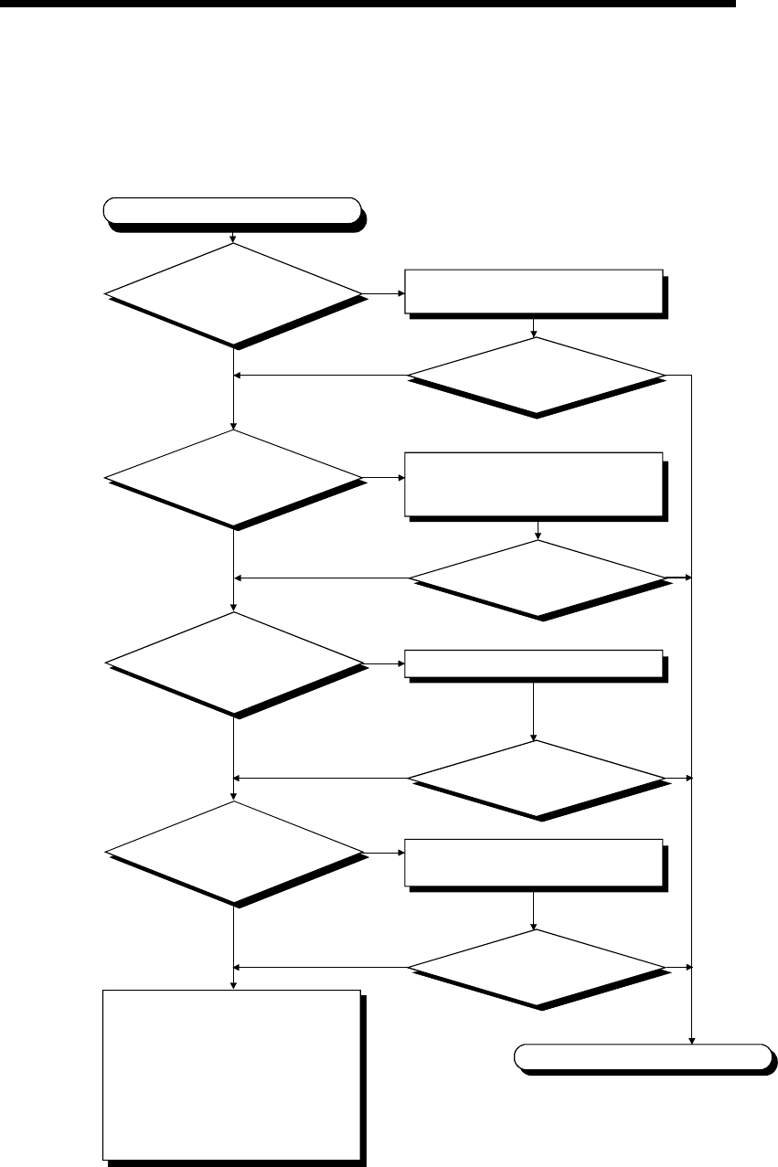
11 - 3 11 - 3
MELSEC-Q
11 TROUBLESHOOTING
11.2.2 Flowchart for when the "MODE" LED is not turned on
The following shows the flowchart to be followed when the "MODE" LED of the CPU
module does not turn on at PLC power-on.
YES
"MODE" LED is not turned on.
Is the power
supply for all the power
supply modules turned on?
Is the wiring of the power supply
module correct?
Check the wire and turn on the
power supply.
Is the "POWER"
LED for the power supply module
turned on?
Exchange the power supply module,
and confirm if "POWER" LED is
turned on.
Connect the extension cable properly.
Completion
NO
YES NO YES
YES
NO
NO
NO YES
YES
Is the
extension cable
connected properly?(Isn't IN
connected to IN or OUT
connected to
OUT?)
Can "MODE" LED
be turned on?
Can "MODE" LED
be turned on?
NO
Set the RESET/L. CLR switch in the
neutral position.
NO YES
Is the CPU module
RESET/L. CLR switch in
the neutral position?
"RESET" position
Neutral position
Can "MODE" LED
be turned on?
Can "MODE" LED
be turned on?
Hardware fault
Check operations in the order
starting from the minimum system.
If the module will not work,
please consult your local Mitsubishi
service center or representative,
explaining a detailed description
of the problem.
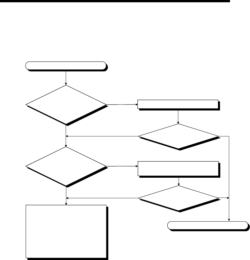
11 - 4 11 - 4
MELSEC-Q
11 TROUBLESHOOTING
11.2.3 Flowchart for when the "MODE" LED is flickering
The following shows the flowchart to be followed when the "MODE" LED of the CPU
module flickers at PLC power-on, at operation start or during operation.
"MODE" LED is flickering
YES
NO
Is the RESET/L.CLR
switch of the CPU module in
the neutral position?
Did you make forced
ON/OFF setting?
Neutral position
Cancel forced ON/OFF.
Hardware fault
Check operations in the order
starting from the minimum system.
If the module will not work,
please consult your local Mitsubishi
service center or representative,
explaining a detailed description
of the problem.
Is the "MODE" LED turned on?
Move the RESET/L.CLR switch to the
neutral position.
RESET position
Is the "MODE" LED turned on?
Completion
NO
NO
YES
YES
11 - 5 11 - 5
MELSEC-Q
11 TROUBLESHOOTING
11.2.4 Flowchart for when the "POWER" LED is turned off
The following shows the flowchart to be followed when the "POWER" LED of the
power supply module turns off at PLC power-on or during operation.
"POWER" LED is turned off.
Please consult your local Mitsubishi
service center or representative,
explaining a detailed description
of the problem.
Is there a power supply? Supply power.
Can "POWER" LED
be turned on?
The supply voltage should be within
the rated range.
Can "POWER" LED
be turned on?
Properly fix the power supply module.
Is the power supply
module fixed?
1) Check the electric-current capacity
and reduce the amount of overcurrent.
2) Turn OFF the input power and wait
several minutes before turning it ON
again.
Is overcurrent
protection and overvoltage
protection working?
Completion
NO
YES NO YES
YES NO YES
NO
YES
NO YES
NO
NO
NO YES
YES
Can "POWER" LED
be turned on?
Can "POWER" LED
be turned on?
Is the power
supply voltage within the
voltage range given in the
specifications?
11 - 6 11 - 6
MELSEC-Q
11 TROUBLESHOOTING
11.2.5 Flowchart for when the "RUN" LED is turned off
The following shows the flowchart to be followed when the "RUN" LED of the CPU
module turns off during PLC operation.
"RUN" LED is turned off.
Reset the CPU module RESET/L.
CLR switch.
Is "ERR." LED
on/flickering?
Considered to be a sequence
program error.
Check the program and modify the
program error location.
(1) PLC part/connection fault
(2) By excessive noise
Proceed to Section 11.2.7,
"Flowchart for when the "ERR." LED
is on/flickering."
Please consult your local Mitsubishi
service center or representative,
explaining a detailed description
of the problem.
Connect a surge protector circuit
such as CR to the noise source.
YES
NO
"RUN" LED
is on.
"RUN" LED is off.
For the case of (1) For the
case of (2)
"RUN" LED does
not turn on.
"RUN" LED is on.
Completion
Can "RUN" LED
be turned on?
YES
NO
Set the CPU module's RUN/STOP
switch to STOP and write END to
address 0 with the GX Developer.
Set the RUN/STOP switch to RUN
and enter to the monitor mode with
the GX Developer to be operated.
Is the "POWER" LED of
the power supply module lit? Proceed to Section 11.2.4,
"Flowchart for when the "POWER"
LED is turned off."
YES
NO
11 - 7 11 - 7
MELSEC-Q
11 TROUBLESHOOTING
11.2.6 When the "RUN" LED is flickering
If the "RUN" LED flickers, follow the steps below.
The High Performance model QCPU flickers the "RUN" LED when the RUN/STOP
switch is set from STOP to RUN after the programs or parameters are written in the
CPU module during the stoppage.
Though this is not the trouble with the CPU module, the operation of the CPU module
is stopped.
To bring the CPU module into RUN status, reset the CPU module with the
RESET/L.CLR or set the RUN/STOP switch again from STOP to RUN.
The "RUN" LED turns on.
11.2.7 Flowchart for when the "ERR." LED is on/flickering
The following shows the flowchart to be followed when the "ERR." LED of the CPU
module turns on or flickers at PLC power-on, at operation start or during operation.
"ERR." LED is on/flickering.
Confirm details of error by
GX Developer.
(Refer to Section 11.3.)
Set the RUN/STOP switch to STOP.
Modify error details.
(Refer to Section 11.3.)
Can the "ERR." LED
be turned off?
Reset by the RESET/L. CLR switch.
Set the RUN/STOP switch to RUN.
Completion
Hardware fault
NO
YES
Please consult your local Mitsubishi
service center or representative,
explaining a detailed description
of the problem.
11 - 8 11 - 8
MELSEC-Q
11 TROUBLESHOOTING
11.2.8 When the "USER" LED is turned on
If the "USER" LED turns on, follow the steps described below.
The "USER" LED turns on when an error is detected by the CHK instruction or the
annunciator (F) turns on.
If the "USER" LED is on, monitor the special relays SM62 and SM80 in the monitor
mode of GX Developer.
• When M62 has turned ON
The annunciator (F) is ON.
Using SD62 to SD79, check the error cause.
• When SM80 has turned ON
The "USER" LED was on by the execution of the CHK instruction.
Using SD80, check the error cause.
Eliminate the error cause after confirming it.
The "USER" LED can be turned off by:
• Making a reset with the RESET/L.CLR switch; or
• Executing the LEDR instruction in the sequence program.
REMARK
When the RESET/L.CLR switch is tilted to L.CLR several times for latch clear
operation, the "USER" LED flickers to indicate that the latch clear processing is
under operation.
When the RESET/L.CLR switch is further tilted to L.CLR while the "USER" LED
flickers, the "USER" LED turns off and terminates the latch clear processing.
11.2.9 When the "BAT." LED is turned on
If the "BAT." LED turns on, follow the steps described below.
The "BAT." LED turns on when a low battery capacity is detected.
If the "BAT." LED is on, monitor the special relays and special registers in the monitor
mode of GX Developer to check which of the CPU module and SRAM card batteries
was lowered in capacity. (SM51 to SM52, SD51 to SD52)
After confirmation, replace the battery with a new one, and reset the CPU module with
the RESET/L.CLR switch or run the LEDR instruction, and the "BAT. " LED will turns
off.
11 - 9 11 - 9
MELSEC-Q
11 TROUBLESHOOTING
11.2.10 Flowchart for when the "BOOT" LED is flickering
The following shows the flowchart to be followed when the "BOOT" LED of the CPU
module flickers at PLC power-on, at operation start or during operation.
"BOOT" LED flickering
Is the "BOOT" LED turned on?
Power off the PLC.
CPU module hardware fault.
Please consult your local Mitsubishi
service center or representative,
explaining a detailed description
of the problem.
Remove the memory card.
Power on the PLC.
Move the DIP switches SW2 and
SW3 of the CPU module to ON.
NO
Completion of automatic write from
memory card to standard ROM
Perform boot operation from
standard ROM.
YES
11 - 10 11 - 10
MELSEC-Q
11 TROUBLESHOOTING
11.2.11 Flowchart for when output module LED is not turned on
The following shows the flowchart to be followed when the output module LED does
not turn on during PLC operation.
Is the LED on when it is
monitored on GX Developer?
YES
Does the output number match?
YES
Is the LED turned on
when another output module
is forcibly turned on?
YES
Is the LED turned
on when the output module is
changed for another output module,
which is then forcibly
turned on?
YES
Output module LED not turned on
Is the "MODE" LED on? Refer to Section 11.2.3.
YES
NO (Flickering)
Reexamine the program.
Change the output number.
NO
NO
NO
NO
Output module hardware fault.
Please consult your local Mitsubishi
service center or representative,
explaining a detailed description
of the problem.
Output module hardware fault
Consult your local system service,
agency or branch office.
CPU module, base unit, extension
cable hardware fault.
Please consult your local Mitsubishi
service center or representative,
explaining a detailed description
of the problem.
Check the input/output number on
the GX Developer system monitor.
11 - 11 11 - 11
MELSEC-Q
11 TROUBLESHOOTING
11.2.12 Flowchart for when output load of output module does not turn on
The following shows the flowchart to be followed when the output load of the output
module does not turn on during PLC operation.
Check output conditions with the
monitor mode of the GX Developer.
Is the operation
indicator of input module
turned on?
Check the power supply load wire
and recover the power supply.
Check the load wire and load, and
recover the power supply.
Change the output relay number and
let the load maximum simultaneous
on current to within the specification.
Voltage measurement among the
modules input and COM terminals.
Check the external wiring and
external input devices.
The output load does not turn on.
Is the operation
indicator of output module
turned on?
Is voltage for the
power supply load
added?
What is the voltage
among the various output
COM terminals of the
output module?
Output module failure
Replace the output module.
Confirm rush current when the load
is at the maximum simultaneous on.
YES
NO
NO
YES
0V
NG
OK
Is it reaching the
supply voltage
value?
On
Off
0V
(Monitor signal off)
Supply voltage
Set the GX Developer in the monitor
mode and check that the input signal
is OFF.
Please consult your local Mitsubishi
service center or representative,
explaining a detailed description
of the problem.
POINT
For the trouble that the input signal to the input module is not turned off,
troubleshoot referring to Section 11.5 Examples of I/O Modules Troubleshooting.
11 - 12 11 - 12
MELSEC-Q
11 TROUBLESHOOTING
11.2.13 Flowchart for when unable to read a program
The following shows the flowchart to be followed when communication with
GX Developer cannot be made during PLC power-on.
The CPU cannot communicate
with the GX Developer.
Is the memory to be
read correct? Select the correct memory.
Can the CPU communicate
with the GX Developer?
Is the connection cable
connected properly? Connect the connection cable properly.
Can the CPU communicate
with the GX Developer?
Completion
NO
YES NO YES
YES NO YES
NO
YES
YES
NO
USB
Is the connection type RS-232?
RS-232 YES
Is the USB driver
installed in the personal
computer?
NO Install the USB driver into the
personal computer.
NO
YES
Can the CPU
communicate with GX Developer by
lowering the baud rate?
NO
Can the CPU communicate
with the GX Developer?
Can the CPU
communicate with the
GX Developer by replacing the
connection cable?
Please consult your local Mitsubishi
service center or representative,
explaining a detailed description
of the problem.
Please consult your local Mitsubishi
service center or representative,
explaining a detailed description
of the problem.
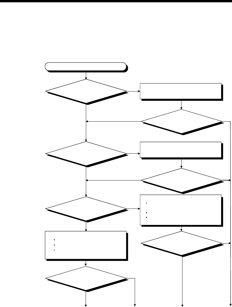
11 - 13 11 - 13
MELSEC-Q
11 TROUBLESHOOTING
11.2.14 Flowchart for when unable to write a program
The following shows the flowchart to be followed when programs cannot be written in
the CPU module.
Unable to write a program
Turn the DIP switch SW1 (system
protect) to OFF.
Is the password registered?
Is the memory program
memory?
OFF NO YES
ON
NO
NO YES
YES
Program memory
YES
Memory
card
Is the DIP switch
SW1 set to OFF?
Is it able to write a program?
3)
NO
YES
1)
NO
Perform the following.
Organize file.
Confirm memory space.
Confirm the writing destination
specification.
2) 3)
Is it able to write a program?
Is it able to write a program?
Is it able to write a program?
Cancel the password using the
GX Developer.
Perform the following.
Confirm whether the write-protect
switch is off or not.
Confirm if it is formatted.
Confirm the writing destination
specification.
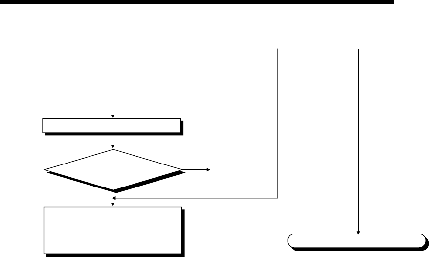
11 - 14 11 - 14
MELSEC-Q
11 TROUBLESHOOTING
Completion
1)
NO
YES
2) 3)
Format program memory.
3)
Is it able to write a program?
Please consult your local Mitsubishi
service center or representative,
explaining a detailed description
of the problem.
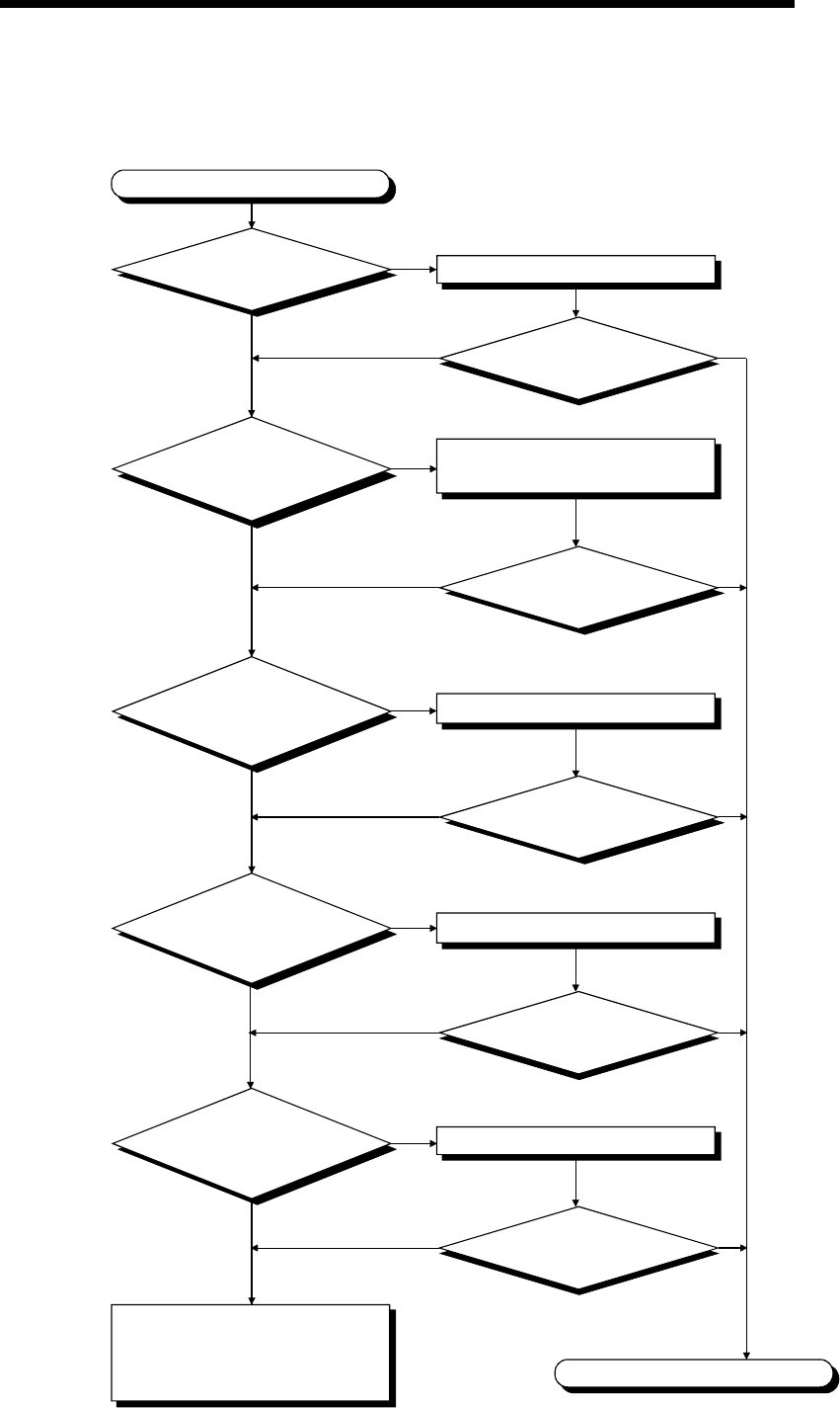
11 - 15 11 - 15
MELSEC-Q
11 TROUBLESHOOTING
11.2.15 Flowchart for when it is unable to perform boot operation from memory card
The following shows the flowchart that must be followed when the boot operation of the
CPU module cannot be performed using the memory card.
Set a file to program setup.
Unable to perform boot operation
Is there CPU module error? Remove the cause of the error.
Is it able to perform
boot operation?
Is the drive that stores
the parameter file specified? Set the DIP switch 2 and 3 to the drive
in which the parameter file is stored.
Set a file to boot file setup.
Is a file set with parameter
boot file setup?
Is a file set with parameter
program setup?
Completion
YES
NO NO YES
YES
NO YES
NO
YES
NO YES
NO
YES
NO YES
NO
Is boot operation
file stored in the
memory card?
YES
NO YES
Write a file to the memory card.
NO
Is it able to perform
boot operation?
Is it able to perform
boot operation?
Is it able to perform
boot operation?
Is it able to perform
boot operation?
Please consult your local Mitsubishi
service center or representative,
explaining a detailed description
of the problem.
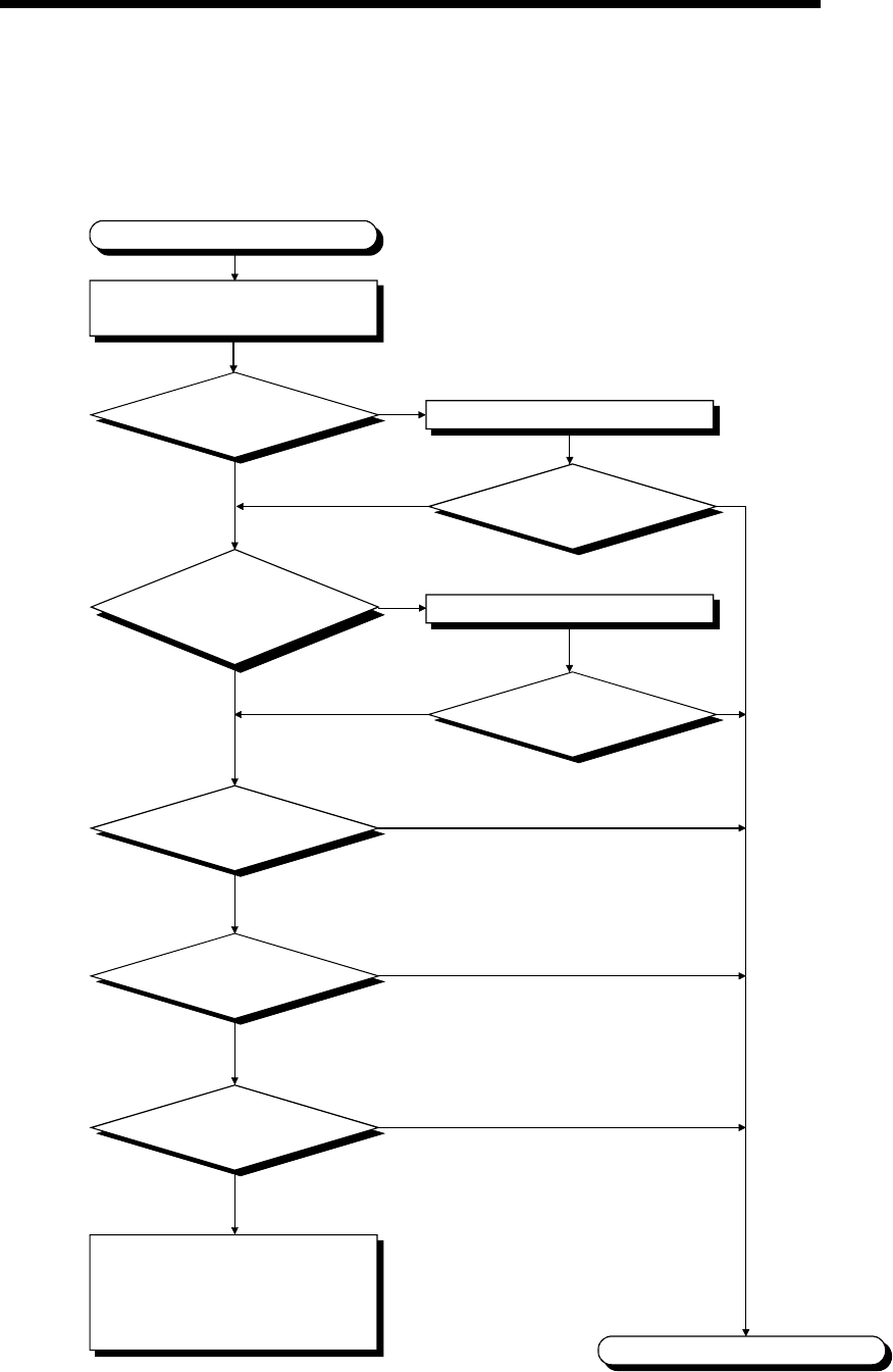
11 - 16 11 - 16
MELSEC-Q
11 TROUBLESHOOTING
11.2.16 Flowchart for when UNIT VERIFY ERR. occurs
The following shows the flowchart to be followed when UNIT VERIFY ERR. occurs at
PLC power-on or during operation.
Is the module of
the applicable slot installed
properly? Install the module properly.
Is the "ERR." LED
turned off?
UNIT. VERIFY ERR. occurs.
NO
YES NO YES
YES
NO YES
NO
Replace the applicable module.
Error detection
Proper operation
Are all the
extension cables of the
base module connected
properly?
Check the slot where error occurred
with the GX Developer.
Replace the CPU module.
Replace the applicable
base unit.
Completion
Hardware fault
Please consult your local Mitsubishi
service center or representative,
explaining a detailed description
of the problem.
Error detection
Error detection
Proper operation
Proper operation
Is the "ERR." LED
turned off?
Install the extension cable properly.
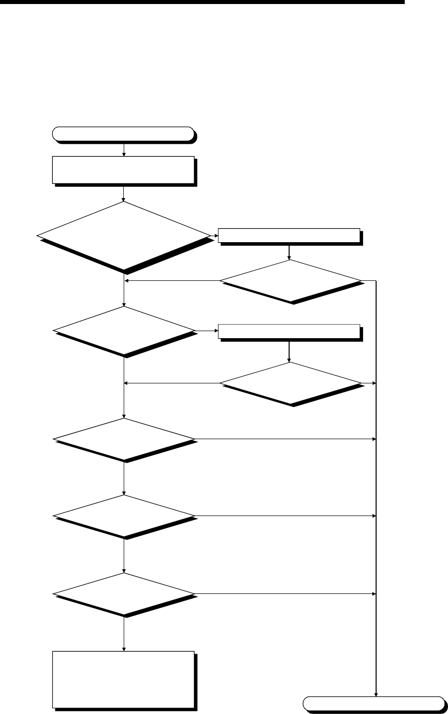
11 - 17 11 - 17
MELSEC-Q
11 TROUBLESHOOTING
11.2.17 Flowchart for when CONTROL BUS ERR. occurs
The following shows the flowchart to be followed when CONTROL BUS ERR. occurs
at PLC power-on or during operation.
This flow chart can be confirmed only when a specific slot/base unit can be detected by
the error code.
Is the module of the
applicable slot installed properly?
Is the extension cable of the
applicable base unit
installed properly?
Install the module and cable properly.
Is the "ERR." LED
turned off?
CONTROL BUS ERR. occurs.
NO
YES NO YES
YES
NO YES
NO
Replace the applicable module.
Are all the extension
cables of the base unit
connected properly?
Check the slot base unit where error
occurred with the GX Developer.
Replace the CPU module.
Error detection
Replace the applicable
base unit.
Proper operation
Completion
Hardware fault
Please consult your local Mitsubishi
service center or representative,
explaining a detailed description
of the problem.
Error detection
Error detection
Proper operation
Proper operation
Install the extension cable properly.
Is the "ERR." LED
turned off?

11 - 18 11 - 18
MELSEC-Q
11 TROUBLESHOOTING
11.3 Error Code List
If a fault occurs when the PLC power supply is switched on, when the CPU is switched
from STOP to RUN or during RUN, the High Performance model QCPU displays an
error (on the LED) using the self-diagnostic function and stores the error information
into the special relays SM and special registers SD.
REMARK
For the error code (4000H to 4FFFH) developed upon a request for general data
processing from the GX Developer, intelligent function module or network system,
refer to Appendix 1.
11.3.1 Procedure for reading error codes
When an error occurs, the error code and error message can be read by the GX
Developer Version 4 or later.
The procedure for reading error codes by the GX Developer is as follows.
1) Start the GX Developer.
2) Connect the CPU module to the personal computer.
3) Select [Online] - [Read from PLC] Menu by the GX Developer, and also read the
project from the High Performance model QCPU.
4) Select the [Diagnostics] - [Diagnostics PLC] Menu.
5) Click the "Error Jump" button in the PLC diagnostics dialog box to display the error
code and error message.
6) Select the [Help] - [PLC error] Menu, and confirm the content of the applicable error
code.
For details of the GX Developer operating method, refer to the applicable the GX
Developer Operating Manual.
11 - 19 11 - 19
MELSEC-Q
11 TROUBLESHOOTING
11.3.2 Error Code List
The following information deals with error codes and the meanings, causes, and corrective
measures of error messages.
"" in the Corresponding CPU column indicates that the error is applied to all types of CPU
modules. "Rem" indicates compatibility with the remote I/O module. A CPU type name in the
column indicates that the error is applied only to the specific CPU module type.
LED Status
Error Code
(SD0) 1 Error Messages Common
Information
(SD5 to 15) 1
Individual
Information
(SD16 to 26) 1 RUN ERROR
Operating
Statuses of
CPU Diagnostic Timing
1000 Off Flicker/On Stop Always
1001
1002
1003
1004
1005
1006
1007
1008
1009
MAIN CPU DOWN ——— ——— Off Flicker Stop Always
1010
1011
1012 END NOT EXECUTE ——— ——— Off Flicker Stop When an END instruction is
executed.
1101
1102
1103
1104
1105
RAM ERROR ——— ——— Off Flicker Stop At power ON/At reset
1200
1201
1202
At power ON/At reset
1203
1204
1205
When END instruction executed.
1206
OPE. CIRCUIT ERR. ——— ——— Off Flicker Stop
When instruction executed.
1300 FUSE BREAK OFF Unit/moule No. ——— Off/ON Flicker/On Stop/
Continue
2
When an END instruction is
executed.
1310 I/O INT ERROR Unit/module No. ——— Off Flicker Stop During interrupt
1 Characters in parentheses ( ) indicate the special register numbers where individual information is being stored.
2 The CPU MODULE operation status when an error occurs can be set at the parameters. (LED display will change accordingly.)
11 - 20 11 - 20
MELSEC-Q
11 TROUBLESHOOTING
Error Code
(SD0) 1 Error Contents and Cause Corrective Action Corres-
ponding
CPU
1000
1001
1002
1003
1004
QCPU
1005 QCPU
Rem
1006
1007
1008
Run mode suspended or failure of main CPU module
(1) Malfunctioning due to noise or other reason
(2) Hardware fault
1009 Failure of the power supply module, CPU module, main base unit,
extension base unit or extension cable is detected.
(1) Measure noise level.
(2) Reset and establish the RUN status again.
If the same error is displayed again, this suggests a CPU
module hardware error. Contact your nearest Mitsubishi
representative.
QCPU
1010
1011
1012
Entire program was executed without the execution of an END
instruction.
(1) When the END instruction is executed it is read as another
instruction code, e.g. due to noise.
(2) The END instruction has been changed to another instruction
code somehow.
(1) Measure noise level.
(2) Reset and establish the RUN status again.
If the same error is displayed again, this suggests a CPU
module hardware error. Contact your nearest Mitsubishi
representative.
1101 Error in internal RAM/program memory where CPU module
sequence program is stored.
1102 Error in RAM used as CPU module work area.
1103 Internal CPU module device error.
1104 RAM Address error in CPU module.
This suggests a CPU module hardware error. Contact your nearest
Mitsubishi representative.
1105 CPU shared memory fault
(1) Measure noise level.
(2) Reset and establish the RUN status again.
If the same error is displayed again, this suggests a CPU
module hardware error. Contact your nearest Mitsubishi
representative.
QCPU
function
Ver. B
or later
1200 The circuit that performs CPU internal index modification is not
operating properly.
1201 Internal CPU module hardware (logic) does not operate normally.
1202 The circuit that executes sequence processing in the CPU module
does not operate properly.
This suggests a CPU module hardware error. Contact your nearest
Mitsubishi representative.
1203 The operation circuit that conducts index modification in the CPU
module is not operating properly.
1204 The hardware (logic) in the CPU us not operating properly.
1205 The operation circuit that conducts sequence processing in the CPU
in not operating properly.
1206 The DSP operation circuit in the CPU is not operating properly.
This suggests a CPU module hardware error. Contact your nearest
Mitsubishi representative. Q4AR
There is an output module with a blown fuse.
(1) Check ERR. LED of the output modules and replace the module
whose LED is lit.
(2) Read the common error information with the peripheral device
and replace the fuse at the output module corresponding to the
numerical value (module No.) reading.
Alternatively, monitor special registers SD1300 to SD1331 with
the peripheral device and change the fuse of the output module
whose bit has a value of "1".
QCPU
Rem
There is an output module with a blown fuse.
(1) Check ERR. LED of the output modules and replace the fuse of
the module whose LED is lit.
(2) Read the common error information with the peripheral device
and replace the fuse at the output module corresponding to the
numerical value (module No.) reading.
Alternatively, monitor special registers SD1300 to SD1331 with
the peripheral device and change the fuse of the output module
whose bit has a value of "1".
QnA
Q4AR
1300
(1) There is an output module with a blown fuse.
(2) External power supply for output load is turned off or
disconnected.
(1) Check ERR. LED of the output modules and replace the module
whose LED is lit.
(2) Read the common error information with the peripheral device
and replace the fuse at the output module corresponding to the
numerical value (module No.) reading.
Alternatively, monitor special registers SD1300 to SD1331 with
the peripheral device and change the fuse of the output module
whose bit has a value of "1".
(3) Check whether the external power supply for output load is ON
or OFF.
Q2AS
1310 An interruption has occurred although there is no interrupt module. One of the individual modules is experiencing hardware problems,
so check the modules. Contact your nearest Mitsubishi
representative and explain the problem with the defective module.
1 Characters in parentheses ( ) indicate the special register numbers where individual information is being stored.
11 - 21 11 - 21
MELSEC-Q
11 TROUBLESHOOTING
Error Code List (Continued)
LED Status
Error Code
(SD0) 1 Error Messages Common
Information
(SD5 to 15) 1
Individual
Information
(SD16 to 26) 1 RUN ERROR
Operating
Statuses of
CPU Diagnostic Timing
At power ON/At reset/
When intelligent function module
is accessed.
1401 SP. UNIT DOWN Unit/module No. ——— Off/On Flicker/On Stop/
Continue
3 At power ON/At reset
When an intelligent function
module access instruction is
executed.
1402 Program error location During execution of FROM/TO
instruction set.
1403
SP. UNIT DOWN Unit/module No.
———
Off/On Flicker/On Stop/
Continue
6
When an END instruction is
executed.
1411 At power ON/At reset
1412
CONTROL-BUS ERR. Unit/module No. Program error location Off Flicker Stop
During execution of FROM/TO
instruction set.
1413 CONTROL-BUS. ERR. ——— ——— off Flicker Stop Always
CONTROL-BUS. ERR. Unit/module No. ——— Off Flicker Stop When an END instruction is
executed.
1414
——— off Flicker Stop
When an END instruction is
executed
1415 Base No. When an END instruction is
executed
1416
CONTROL-BUS. ERR.
Unit/module No.
———
Off Flicker Stop
At power ON/At reset
1421 SYS. UNIT DOWN 3 ——— ——— off Flicker Stop Always
1500 AC DOWN ——— ——— On Off Continue Always
1510 DUAL DC DOWN
5V 4 ——— ——— on on Continue Always
1520 DC DOWN 5V 5 ——— ——— off Flicker Stop Always
1530 DC DOWN 24V 3 ——— ——— on on Continue Always
1600 ON On
1601
1602
BATTERY ERROR Drive Name ———
BAT.ALM LED On
Continue Always
2000 UNIT VERIFY ERR. Unit/module No. ——— Off/On Flicker/On Stop/
Continue
2
When an END instruction is
executed.
1 Characters in parentheses ( ) indicate the special register numbers where individual information is being stored.
2 The CPU module operation status when an error occurs can be set at the parameters. (LED display will change accordingly.)
3 This can only be detected in redundant systems. Detection is possible in either the control system or the standby system.
4 This can only be detected in the redundant system control system.
5 This can be detected in either a standalone system or a redundant system. However, in a redundant system it can only be detected in the control system.
6 Stop/continue operation is selectable for each module by setting parameters.

11 - 22 11 - 22
MELSEC-Q
11 TROUBLESHOOTING
Error Code
(SD0) 1 Error Contents and Cause Corrective Action Corres-
ponding
CPU
• There was no response from the intelligent function module during
initial communication stage.
• The size of the buffer memory of the intelligent function module is
wrong.
The CPU module is experiencing hardware problems. Contact your
nearest Mitsubishi representative. QCPU
Rem
1401 When parameter I/O allocation was being made, there was no
return signal from the special function module during initial
processing stage.
When error is generated, the initial I/O number of the special
function module that corresponds to the common information is
stored.
The special function module that was being accessed is
experiencing hardware problems. Contact your nearest Mitsubishi
representative. QnA
The intelligent function module was accessed in the program, but
there was no response. This suggests a CPU module hardware error. Contact your nearest
Mitsubishi representative. QCPU
Rem
1402 The special function module was accessed during the execution of
a FROM/TO instruction set, but there was no response.
When an error is generated, the program error location
corresponding to the individual information is stored.
The special function module that was being accessed is
experiencing hardware problems. Contact your nearest Mitsubishi
representative. QnA
1403 • There was no response from the intelligent function module when
the END instruction is executed.
• An error is detected at the intelligent function module.
The intelligent function module that was being accessed is
experiencing hardware problems. Contact your nearest Mitsubishi
representative.
QCPU
Rem
1411
When performing a parameter I/O allocation a special function
module could not be accessed during initial communications.
On error occurring, the head I/O number of the corresponding
special function module is stored in the common information.
Rem
1412
The FROM/TO instruction set could not be executed, due to a
system bus error with a special function module.
On error occurring, the program error location is stored in the
individual information.
A special function module, the CPU module, or the base unit is
experiencing problems. Contact your nearest Mitsubishi
representative.
The High Performance model QCPU of function version A was
loaded in a multiple CPU system configuration.
(1) Change the High Performance model QCPU of function version
A for the High Performance model QCPU of function version B.
(2) An intelligent function module, CPU module or the base unit is
experiencing problems. Contact your nearest Mitsubishi
representative.
QCPU
function
Ver. B
or later
1413
An error is detected on the system bus.
• Wait-length time-out, arbitration time-out.
An intelligent function module, the CPU module, or the base unit is
experiencing problems. Contact your nearest Mitsubishi
representative.
QCPU
Rem
Fault of the loaded module was detected.
The High Performance model QCPU of function version A was
loaded in a multiple CPU system configuration.
(1) Change the High Performance model QCPU of function version
A for the High Performance model QCPU of function version B.
(2) An intelligent function module, CPU module or the base unit is
experiencing problems. Contact your nearest Mitsubishi
representative.
QCPU
function
Ver. B
or later
1414
An error is detected on the system bus. An intelligent function module, the CPU module, or the base unit is
experiencing problems. Contact your nearest Mitsubishi
representative.
QCPU
Rem
1415 Fault of the main or extension base unit was detected.
1416 System bus fault was detected at PLC power-on or CPU module
reset.
An intelligent function module, CPU module or the base unit is
experiencing problems. Contact your nearest Mitsubishi
representative.
QCPU
function
Ver. B
or later
1421 Hardware fault at the system management module AS92R. This is experiencing hardware problems.
Contact your nearest Mitsubishi representative. Q4AR
1500 A momentary power supply interruption has occurred.
The power supply went off. Check the power supply.
Rem
1510 The 5 VDC supplied to one of the two power-supply modules in the
redundant system extension base unit has dropped below 85% of
the rated voltage.
1520 The 5 VDC supplied to the power-supply modules in the extension
base unit has dropped below 80% of the rated voltage.
Check the supply voltage of the power supply module. If the voltage
is abnormal then replace the power supply module.
1530 The 24 VDC power supplied to the system management module
AS92R has dropped below 85% of the rated voltage. Check the power supply.
Q4AR
1600 (1) Voltage in the CPU module battery.
(2) The CPU module battery is not connected.
(1) Change the battery.
(2) If the battery is for program memory, standard RAM or for the
back-up power function, install a lead connector.
1601 Voltage of the battery on memory card 1 has dropped below
stipulated level. Change the battery.
1602 Voltage of the battery on memory card 2 has dropped below
stipulated level. Change the battery. QnA
I/O module information power ON is changed.
I/O module (or special function module) not installed properly or
installed on the base unit.
Read the error common information at the peripheral device, and
check and/or change the module that corresponds to the numerical
value (module number) there.
Alternatively, monitor the special registers SD1400 to SD1431 at a
peripheral device, and change the fuse at the output module whose
bit has a value of "1".
Rem
2000
The High Performance model QCPU of function version A was
loaded in a multiple CPU system configuration. Change the High Performance model QCPU of function version A
for the High Performance model QCPU of function version B.
QCPU
function
Ver. B
or later
1 Characters in parentheses ( ) indicate the special register numbers where individual information is being stored.

11 - 23 11 - 23
MELSEC-Q
11 TROUBLESHOOTING
Error Code List (Continued)
LED Status
Error Code
(SD0) 1 Error Messages Common
Information
(SD5 to 15) 1
Individual
Information
(SD16 to 26) 1 RUN ERROR
Operating
Statuses of
CPU Diagnostic Timing
2100
2101
SP. UNIT LAY ERR. Unit/module No. ——— Off Flicker Stop At power ON/At reset
2102
2103
2104
2105
SP. UNIT LAY ERR. Unit/module No. ——— Off Flicker Stop At power ON/At reset
2106 SP. UNIT LAY ERR. Unit/module No. ——— Off Flicker Stop At power ON/At reset
2107
2108
2109 6
SP. UNIT LAY ERR. Unit/module No. ——— Off Flicker Stop At power ON/At reset
1 Characters in parentheses ( ) indicate the special register numbers where individual information is being stored.
6 This can only be detected in the redundant system standby system.
11 - 24 11 - 24
MELSEC-Q
11 TROUBLESHOOTING
Error Code
(SD0) 1 Error Contents and Cause Corrective Action Corres-
ponding
CPU
Slot loaded with the QI60 is set to other than the Inteli (intelligent
function module) or Interrupt (interrupt module) in the parameter I/O
assignment.
Make setting again to match the parameter I/O assignment with the
actual loading status.
QCPU
function
Ver. B
or later
(1) In the parameter I/O allocation settings, an Inteli (intelligent
function module) was allocated to a location reserved for an I/O
module or vice versa.
(2) In the parameter I/O allocation settings, a module other than
CPU (or nothing) was allocated to a location reserved for a CPU
module or vice versa.
(3) A general-purpose switch was set to the module with no
general-purpose switches.
(1) Reset the parameter I/O allocation setting to conform to the
actual status of the intelligent function module and the CPU
module.
(2) Delete the general-purpose switch settings.
QCPU
Rem
2100
In parameter I/O allocation settings, a special function module was
allocated to a location reserved for an I/O module. Or, the opposite
has happened.
Reset the parameter I/O allocation setting to conform with the actual
status of the special function modules. QnA
13 or more A-series special function modules (except for the QI60,
A1SI61) that can initiate an interrupt to the CPU module have been
installed.
Keep the number of A-series special function modules that can
initiate an interrupt (except for the QI60, A1SI61) to 12 or fewer. QCPU
2101 13 or more special function modules (not counting the AI61)
capable of sending an interrupt to the CPU module have been
installed.
Keep the number of special function modules that can initiate an
interrupt (with the exception of the AI61 module) to 12 or fewer. QnA
7 or more A1SD51S have been installed. Keep the number of A1SD51S to 6 or fewer. QCPU
2102 7 or more computer link modules (excludes A (1S) J71QC24) have
been installed. Keep the number of computer link modules (excludes A (1S)
J71QU24) installed to 6 or fewer. QnA
Rem
(1) Two or more QI60/A1SI61 modules are loaded in a single-PLC
system.
(2) Two or more QI60/A1SI61 modules are set to the same control
PLC in a multiple CPU system.
(3) Two or more A1SI61 modules are loaded in a multiple CPU
system.
(1) Reduce the number of QI60/A1SI61 modules loaded in the
single-PLC system to one.
(2) Change the number of QI60/A1SI61 modules set to the same
control PLC to only one in the multiple CPU system.
(3) Reduce the number of A1SI61 modules to only one in the
multiple CPU system.
When using an interrupt module with each QCPU in a multiple
CPU system, change it for the QI60. (Use one A1SI61 module +
max. three QI60 modules or only the QI60 modules.)
QCPU
function
Ver. B
or later
Two or more QI60, A1SI61 interrupt modules have been installed. Install only 1 QI60, A(1S)I61 module. QCPU
The QI60 is loaded. Remove the QI60. Rem
2103
Two or more AIS61 interrupt modules have been installed. Install only 1 AI61 module. QnA
2104 At the MELSECNET/MINI auto refresh parameter settings, the
module allocation that was set is different from the actual module
models at the station numbers in the link system.
Reset the parameter MELSECNET/MINI auto refresh unit module
allocation setting so that it conforms to the station number of the
module that is actually linked. QnA
2105
There are too many special function modules that can use
dedicated instructions allocated (number of modules installed).
(The total of the figures indicated below is above 1344.)
(Number of AD59 modules installed × 5)
(Number of AD57 (S1)/AD58 modules installed × 8)
(Number of AJ71C24 (S3/S6/S8) modules installed × 10)
(Number of AJ71UC24 modules installed × 10)
(Number of AJ71C21 (S1) modules installed × 29)
(Number of AJ71PT32-S3/AJ71T32-S3 modules installed × 125)
(Number of AJ71QC24 (R2, R4) modules installed × 29)
(Number of AJ71ID1 (2)-R4 modules installed × 18)
(Number of AD75 modules installed × 12)
Total > 1344
Reduce the number of special function modules installed.
: When the expansion mode is used. QnA
• Five or more MELSECNET/H modules are loaded in a whole
multiple CPU system.
• Five or more Q series Ethernet interface modules are loaded in a
whole multiple CPU system.
Reduce the number of modules to four or less in the whole multiple
CPU system.
QCPU
function
Ver. B
or later
(1) 5 or more MELSECNET/H modules have been installed.
(2) 5 or more Q series Ethernet interface modules have been
installed.
(3) Identical network numbers or station numbers exist in the
MELSECNET/10 network system.
(1) Keep the number to 4 or fewer.
(2) Keep the number to 4 or fewer.
(3) Check the network numbers and station numbers.
QCPU
Rem
2106 (1) 5 or more AJ71QLP21 & AJ71QBR11 modules are installed.
(2) 3 or more AJ71AP21/R21 & AJ71AT21B modules are installed.
(3) The total number of installed AJ71QLP21, AJ71QBR11,
AJ71AP21/R21, and AJ71AT21B modules exceeds 5.
(4) Identical network Nos. or identical station Nos. exist at the
MELSECNET/10 network system.
(5) 2 or more master or load stations exist simultaneously at the
MELSECNET(II) or MELSECNET/B data link system.
(1) Install 4 or fewer modules.
(2) Install 2 or fewer modules.
(3) Reduce the total number of modulees to 4 or less.
(4) Check the network Nos. and station Nos.
(5) Check the station Nos.
QnA
2107 Head X/Y set in the parameter I/O allocation settings is also the
head X/Y for another module. Reset the parameter I/O allocation setting to conform with the actual
status of the special function modules.
Rem
(1) Network module A1SJ71LP21, A1SJ71BR11, A1SJ71AP21 ,
A1SJ71AR21, or A1SJ71AT2B dedicated for the A2USCPU
has been installed.
(2) Network module A1SJ71QLP21 or A1SJ71QBR11 dedicated for
the Q2AS has been installed.
Change network module to QJ71LP21 or QJ71BR11. QCPU
2108
A(1s)J71LP21 or A(1s)J71BR11 for use with the AnUCPU network
module has been installed. Change network module to A(1s)J71QLP21 or A(1s)J71QBR11. QnA
2109 6 The control system and standby system module configurations are
different when a redundant system is in the backup mode. Check the module configuration of the standby system. Q4AR
1 Characters in parentheses ( ) indicate the special register numbers where individual information is being stored.
6 This can only be detected in the redundant system standby system.
11 - 25 11 - 25
MELSEC-Q
11 TROUBLESHOOTING
Error Code List (Continued)
LED Status
Error Code
(SD0) 1 Error Messages Common
Information
(SD5 to 15) 1
Individual
Information
(SD16 to 26) 1 RUN ERROR
Operating
Statuses of
CPU Diagnostic Timing
2110
2111
SP. UNIT ERROR Unit/module No. Program error location Off/On Flicker/On Stop/
Continue
2 When instruction executed.
2112 Unit/module No.
2113
SP. UNIT ERROR
FFFFH (fixed)
Program error location Off/On Flicker/On Stop/
Continue
2
When instruction executed/
STOP RUN
2114
2115
2116
2117
SP. UNIT ERROR Unit/module No. Program error location Flicker/On Flicker/On Continue/
Stop When instruction is executed
2120
2121
2122
2124
2125
SP. UNIT LAY ERR. ——— ——— Off Flicker Stop At power ON/At reset
2126 SP. UNIT LAY ERR. Unit/module No. ——— Off Flicker Stop At power ON/At reset
2150 SP. UNIT VER. ERR. Unit/module No. ——— Off Flicker Stop At power ON/At reset
2200 MISSING PARA. Drive Name ——— Off Flicker Stop At power ON/At reset
2210 BOOT ERROR Drive Name ——— Off Flicker Stop At power ON/At reset
2300
2301
2302
ICM. OPE. ERROR Drive Name ——— Off/On Flicker/On Stop/
Continue
2
When memory card is inserted or
removed
2400 FILE SET ERROR File name Parameter number Off Flicker Stop At power ON/At reset
1 Characters in parentheses ( ) indicate the special register numbers where individual information is being stored.
2 The CPU module operation status when an error occurs can be set at the parameters. (LED display will change accordingly.)
11 - 26 11 - 26
MELSEC-Q
11 TROUBLESHOOTING
Error Code
(SD0) 1 Error Contents and Cause Corrective Action Corres-
ponding
CPU
Station not loaded was specified using the instruction whose target
was the PLC share memory.
Read the individual information of the error, check the program
corresponding that value (program error location), and make
correction.
QCPU
function
Ver. B
or later
2110 (1) The location designated by the FROM/TO instruction set is not a
special function module.
(2) The special function module, Network module being accessed is
faulty.
2111 The location designated by a link direct device (J \) is not a
network module.
(1) Read error individual information, then check and edit the
FROM/TO instruction set that corresponds to the numerical
value there (Program error location).
(2) The special function module that is being accessed has a
hardware error. Consult the nearest service center, agent or our
branch office and describe the symptom.
2112
(1) The location designated by a special function module dedicated
instruction is not a special function module.
(2) The network number specified by the network dedicated
instruction does not exist, or the network module is not the
corresponding one.
(3) Alternatively, it is not the relevant special function module.
Rem
2113 The one specified in the network-dedicated instruction is not a
network module, or a relay target network does not exist.
Read error individual information, then check and edit the special
function module (Network module) dedicated instruction that
corresponds to the numerical value there (program error location).
2114 An instruction, which on execution specifies other stations, has
been used for specifying the host station. (An instruction that does
not allow the host station to be specified).
2115 An instruction, which on execution specifies the host station, has
been used for specifying other stations. (An instruction that does not
allow other stations to be specified).
2116
• An instruction that does not allow the module under the control of
another station to be specified is being used for a similar task.
• Instruction was executed for the A or QnA module under control of
another station.
2117 A CPU module that cannot be specified in the instruction dedicated
to the multiple CPU system was specified.
Read the individual information of the error, check the program
corresponding that value (program error location), and make
correction.
QCPU
function
Ver. B
or later
2120 The location of Q B and QA1S B is improper. Check the location of the base unit.
2121 The CPU module is installed at other than the CPU slot or slots 0 to
2. Check the loading position of the CPU module and reinstall it at the
correct slot.
2122 QA1S B is used to the main base unit. Use Q3 B as the main base unit.
2124
(1) A module is installed at 65th or higher slot.
(2) A module is installed at the slot later than the number of slots
specified with base allocation setting.
(3) A module is installed at the I/O points later than the 4,096th
point.
(4) A module installed at the 4,096th point occupies higher points.
(1) Remove the module installed at 65th or later slot.
(2) Remove the module installed at the slot later than the number of
slots specified with base allocation setting.
(3) Remove the module installed at the I/O points later than the
4,096th point.
(4) Change the last module to a module which does not exceed the
4,096th point.
2125 (1) A module which the QCPU cannot recognise has been installed.
(2) There was no response form the intelligent function module.
(1) Install a module which can be used with the CPU.
(2) The intelligent function module is experiencing hardware
problems. Contact your nearest Mitsubishi representative.
QCPU
Rem
2126
CPU module locations in a multiple CPU system are either of the
following.
(1) There are empty slots between the QCPU and QCPU/motion
controller.
(2) Modules other than the QCPU (including the motion controller)
modules are loaded between the QCPU modules.
(1) Eliminate empty slots between the CPU modules. (Set empty
slots on the right side of the CPU modules.)
(2) Remove the modules, which are not the QCPU modules, loaded
between the QCPU modules, and fit the slots with the QCPUs.
Load the motion controller modules on the right side of the
QCPUs.
2150 In a multiple CPU system, the control PLC of the intelligent function
module incompatible with the multiple CPU system is set to other
than station 1.
(1) Change the intelligent function module for the one compatible
with the multiple CPU system (function version B).
(2) Change the setting of the control CPU of the intelligent function
module incompatible with the multiple CPU system to station 1.
QCPU
function
Ver. B
or later
2200 There is no parameter file at the drive designated by DIP switches
as a valid drive.
Check and correct the setting of the parameter enabled drive
switch.
Put a parameter file in the drive designated by the parameter
enabled drive switch.
The contents of the boot file are incorrect. Check the boot setting. QCPU
2210 There is no boot file in the drive designated by the parameter
enabled drive switch even though the Boot DIP switch is ON.
Check and correct the setting of the parameter enabled drive
switch.
Put a boot file in the drive designated by the parameter enabled
drive switch.
QnA
2300
(1) A memory card was removed without switching the memory
card in/out switch OFF.
(2) The memory card in/out switch is turned ON although a memory
card is not actually installed.
(1) Remove memory card after placing the memory card in/out
switch OFF.
(2) Turn on the card insert switch after inserting a memory card.
2301 (1) The memory card has not been formatted.
(2) Memory card format status is incorrect.
2302 A memory card that cannot be used with the CPU module has been
installed.
(1) Format memory card.
(2) Reformat memory card.
Check memory card.
Automatic write to standard ROM was performed on the CPU
module that is incompatible with automatic write to standard ROM.
(Memory card where automatic write to standard ROM was
selected in the boot file was fitted and the parameter enable drive
was set to the memory card.)
(1) Execute automatic write to standard ROM on the CPU module
which is compatible with automatic write to standard ROM.
(2) Using GX Developer, perform write of parameters and programs
to standard ROM.
(3) Change the memory card for the one where automatic write to
standard ROM has not been set, and perform boot operation
from the memory card.
QCPU
function
Ver. B
or later
The file designated at the PLC file settings in the parameters cannot
be found.
Read the error individual information at the peripheral device, check
to be sure that the parameter drive name and file name correspond
to the numerical values there (parameter number), and correct.
Create a file created using parameters, and load it to the CPU
module.
2400
The Ethernet parameter that was added for QnACPU, with the
function version "B," has been set to QnACPU without the function
version "B."
Change to QnACPU with the function version "B." Delete the
Ethernet parameter. QnA
1 Characters in parentheses ( ) indicate the special register numbers where individual information is being stored.
11 - 27 11 - 27
MELSEC-Q
11 TROUBLESHOOTING
Error Code List (Continued)
LED Status
Error Code
(SD0) 1 Error Messages Common
Information
(SD5 to 15) 1
Individual
Information
(SD16 to 26) 1 RUN ERROR
Operating
Statuses of
CPU Diagnostic Timing
2401 FILE SET ERROR File name Parameter number Off Flicker Stop At power ON/At reset
2410
2411
2412
2413
FILE OPE. ERROR File name Program error location Off/On Flicker/ON Stop/
Continue
2 When instruction is executed
2500
2501
2502
2503
2504
CAN'T EXE. PRG. File name ——— Off Flicker Stop At power ON/At reset
3000
3001
3002
PARAMETER ERROR File name Parameter number Off Flicker Stop At power ON/Reset/
STOP RUN
PARAMETER ERROR File name/drive name Parameter number Off Flicker Stop When an END instruction is
executed.
3003
PARAMETER ERROR File name Parameter number Off Flicker Stop At power ON/Reset/
STOP RUN
3004 PARAMETER ERROR File name Parameter number Off Flicker Stop At power ON/Reset/
STOP RUN
3006 PARAMETER ERROR File name Parameter number Off Flicker Stop At power ON/Reset/
STOP RUN
3009
3010
3012
3013
PARAMETER ERROR File name/drive name Parameter number Off Flicker Stop At power ON/Reset/
STOP RUN
1 Characters in parentheses ( ) indicate the special register numbers where individual information is being stored.
2 The CPU module operation status when an error occurs can be set at the parameters. (LED display will change accordingly.)
11 - 28 11 - 28
MELSEC-Q
11 TROUBLESHOOTING
Error Code
(SD0) 1 Error Contents and Cause Corrective Action Corres-
ponding
CPU
Program memory capacity was exceeded by performing boot
operation or automatic write to standard ROM.
(1) Check and correct the parameters (boot setting).
(2) Delete unnecessary files in the program memory.
(3) Choose "Clear program memory" for boot in the parameter so
that boot is started after the program memory is cleared.
QCPU
function
Ver. B
or later
2401
The file designated at the parameter PLC RAS settings fault history
area has not been created.
Read the error individual information at the peripheral device, check
to be sure that the parameter drive name and file name correspond
to the numerical values there (parameter number), and correct.
Check the space remaining in the memory card.
2410 The file designated by the sequence program cannot be found.
Read the error individual information at the peripheral device, check
to be sure that the program corresponds to the numerical values
there (program location), and correct.
Create a file created using parameters, and load it to the CPU
module.
2411 The sequence program designated a file that cannot be designated
by the sequence program (comment file, etc.).
2412 The SFC program file is one that cannot be designated by the
sequence program.
Read the error individual information at the peripheral device, check
to be sure that the program corresponds to the numerical values
there (program location), and correct.
2413 No data has been written to the file designated by the sequence
program.
Read the error individual information at the peripheral device, check
to be sure that the program corresponds to the numerical values
there (program location), and correct.
Check to ensure that the designated file has not been write protected.
2500 There is a program file that uses a device that exceeds the device
allocation range designated by the parameter device settings.
Read the error common information at the peripheral device, check
to be sure that the parameter device allocation setting and the
program file device allocation correspond to the numerical values
there (file name), and correct if necessary.
2501 There are multiple program files although "none" has been set at
the parameter program settings. Edit the parameter program setting to "yes".
Alternatively, delete unneeded programs.
2502 The program file is incorrect.
Alternatively, the file contents are not those of a sequence program. Check whether the program version is .QPG, and check the
file contents to be sure they are for a sequence program.
2503
2504
There are no program files at all.
Two or more SFC normal programs or control programs have been
designated.
Check program configuration.
Check parameters and program configuration.
In a multiple CPU system, the intelligent function module under
control of another station is specified in the interrupt pointer setting
of the parameter.
(1) Specify the first I/O number of the intelligent function module
under control of the host station.
(2) Delete the interrupt pointer setting of the parameter.
QCPU
function
Ver. B
or later
3000 The parameter settings for timer time limit setting, the RUN-PAUSE
contact, the common pointer number, the general data processing,
number of vacant slots, or system interrupt settings are outside the
range that can be used by the CPU module.
3001 Parameter contents have been destroyed.
Rem
3002 When "use the following files" is selected for the file registers in the
PLC file setting parameter, the specified file does not exist though
the file register capacity has been set.
(1) Read the error detailed information at the peripheral device,
check the parameter items corresponding to the numerical
values (parameter numbers) there, and correct when necessary.
(2) If the error is still generated following the correction of the
parameter settings, it is likely that there is a memory error, either
in the internal CPU RAM/program memory or on the memory
card. Contact your nearest Mitsubishi representative.
The automatic refresh range of the multiple CPU system exceeded
the file register capacity. Change the file register file for the one refresh-enabled in the whole
range.
QCPU
function
Ver. B
or later
3003
The number of devices set at the parameter device settings
exceeds the possible CPU module range.
(1) Read the error detailed information at the peripheral device,
check the parameter items corresponding to the numerical
values (parameter numbers) there, and correct when necessary.
(2) If the error is still generated following the correction of the
parameter settings, it is likely that there is a memory error, either
in the internal CPU RAM/program memory or on the memory
card. Contact your nearest Mitsubishi representative.
3004 The parameter file is incorrect.
Alternatively, the contents of the file are not parameters. Check whether the parameter file version is .QPA, and
check the file contents to be sure they are parameters.
3006
(1) The high speed interrupt parameter is set in a Q02CPU.
(2) The high speed parameter is set in a multiple CPU system.
(3) The high speed interrupt parameter is set when a QA1S B or
QA B is used.
(4) No module is installed at the I/O address designated by the high
speed interrupt parameter.
(1) Delete the setting of the Q02CPU’s high speed interrupt
parameter. To use high speed interrupts, change the CPU
module to one of the Q02H/Q06H/Q12H/Q25HCPU.
(2) To use a multiple CPU system, delete the setting of the high-
speed interrupt parameter. To use high speed interrupts, change
the system to a single PLC system.
(3) To use either the QA1S B or QA B, delete the setting of the
high speed interrupt parameter. To use high speed interrupts, do
not use the QA1S B/QA B.
(4) Re-examine the I/O address designated by the high speed
interrupt parameter.
QCPU
serial
No.
04012
or later
3009 A modules are set to control PLCs in a multiple CPU system. Re-set the parameter I/O assignment to control them under one
QCPU. (Change the parameters of all stations in the multiple CPU
system.)
3010 The parameter-set number of CPU modules differs from the actual
number in a multiple CPU system. Match (preset count of multiple PLC setting) - (CPU (empty) setting
in I/O assignment) with the actual number of CPUs loaded.
3012 Multiple CPU setting or control PLC setting differs from that of the
reference station in a multiple CPU system. Match the multiple PLC setting or control CPU setting in the
parameter with that of the reference station (station 1).
3013
Multiple CPU automatic refresh setting is any of the followings in a
multiple CPU system.
(1) When a bit device is specified as a refresh device, a number
other than a multiple of 16 is specified for the refresh-starting
device.
(2) The device specified is other than the one that may be specified.
(3) The number of send points is an odd number.
Check the following in the multiple CPU automatic refresh
parameters and make correction.
(1) When specifying the bit device, specify a multiple of 16 for the
refresh starting device.
(2) Specify the device that may be specified for the refresh device.
(3) Set the number of send points to an even number.
QCPU
function
Ver. B
or later
1 Characters in parentheses ( ) indicate the special register numbers where individual information is being stored.
11 - 29 11 - 29
MELSEC-Q
11 TROUBLESHOOTING
Error Code List (Continued)
LED Status
Error Code
(SD0) 1 Error Messages Common
Information
(SD5 to 15) 1
Individual
Information
(SD16 to 26) 1 RUN ERROR
Operating
Statuses of
CPU Diagnostic Timing
3100 LINK PARA. ERROR File name Parameter number Off Flicker Stop At power ON/Reset/
STOP RUN
LINK PARA. ERROR File name/drive name Parameter number Off Flicker Stop When an END instruction is
executed.
3101
3102
3103
3104
3105
LINK PARA. ERROR File name Parameter number Off Flicker Stop At power ON/Reset/
STOP RUN
LINK PARA. ERROR File name/drive name Parameter number Off Flicker Stop When an END instruction is
executed.
3106
LINK PARA. ERROR File name Parameter number Off Flicker Stop At power ON/Reset/
STOP RUN
3107 LINK PARA. ERROR File name Parameter number Off Flicker Stop At power ON/Reset/
STOP RUN
3200
3201
3202
3203
SFC PARA. ERROR File name Parameter number Off Flicker Stop STOP RUN
3300 SP. PARA. ERROR File name Parameter number Off Flicker Stop At power ON/Reset/
STOP RUN
1 Characters in parentheses ( ) indicate the special register numbers where individual information is being stored.
11 - 30 11 - 30
MELSEC-Q
11 TROUBLESHOOTING
Error Code
(SD0) 1 Error Contents and Cause Corrective Action Corres-
ponding
CPU
In a multiple CPU system, the MELSECNET/H under control of
another station is specified as the first I/O number in the network
setting parameter of the MELSECNET/H.
(1) Delete the MELSECNET/H network parameter of the
MELSECNET/H under control of another station.
(2) Change the setting to the first I/O number of the MELSECNET/H
under control of the host station.
The network parameters of the MELSECNET/H operating in the
ordinary station were rewritten to the control station, or the network
parameters of the MELSECNET/H operating in the control station
were rewritten to the ordinary station.
(The network parameters are reflected on the module side by
making a reset.)
Reset the CPU module.
QCPU
function
Ver. B
or later
(1) The number of actually installed modules is different from that
designated in the number of modules setting parameter of
MELSECNET/H.
(2) The head I/O number of actually installed modules is different
from that designated in the network parameter of
MELSECNET/H.
(3) Some data in the parameter cannot be handled.
(4) The station type of MELSECNET/H has been changed while the
power is on. (RESET RUN is required to change the station
type.)
(1) Check the network parameters and the installation state. If
inconsistency is found, arrange consistency between network
parameters and the installation state.
If network parameters are changed, write the new network
parameters to the CPU module.
(2) Check the number of extension stages of the extension base unit.
(3) Check the state of connection of the extension base unit and
connector. If the display unit is connected to the main base unit
or extension base unit, check the state of connection.
(4) If the error persists after the above items (1) through (3) are
checked, the hardware is faulty. Contact your nearest Mitsubishi
representative and explain the symptom.
QCPU
3100
Network parameters have not been written although the QnACPU is
the control station, or the master station. (1) Write after correcting network parameters.
(2) If the error persists after corrections have been made, contact
your nearest Mitsubishi representative. QnA
The link refresh range exceeded the file register capacity. Change the file register file for the one refresh-enabled in the whole
range.
• When the station number of the MELSECNET/H module is 0, the
inter-PLC network parameter setting has been made.
• When the station number of the MELSECNET/H module is other
than 0, the remote master parameter setting has been made.
Correct the type or station number of the MELSECNET/H module in
the parameter to meet the used system.
QCPU
function
Ver. B
or later
3101 The network No. specified by a parameter is different from that of
the actually mounted network.
The head I/O No. specified by a parameter is different from that of
the actually mounted I/O unit.
The network class specified by a parameter is different from that of
the actually mounted network.
The network refresh parameter of the MELSECNET/10(H) is out of
the specified area.
(1) Check the network parameters and the installation state. If
inconsistency is found, arrange consistency between network
parameters and the installation state.
If network parameters are changed, write the new network
parameters to the CPU module.
(2) Check the number of extension stages of the extension base unit.
(3) Check the state of connection of the extension base unit and
connector. If the display unit is connected to the main base unit
or extension base unit, check the state of connection.
(4) If the error persists after the above items (1) through (3) are
checked, the hardware is faulty. Contact your nearest Mitsubishi
representative and explain the symptom.
3102 An error was discovered when the network parameter check was
made at the network module. (1) Write after correcting network parameters.
(2) If the error persists after corrections have been made, contact
your nearest Mitsubishi representative.
In a multiple CPU system, the Q series Ethernet interface module
under control of another station is specified as the first I/O number
of the Ethernet setting parameter.
(1) Delete the Ethernet setting parameter of the Q series Ethernet
interface module under control of another station.
(2) Change the setting to the first I/O number of the Q series
Ethernet interface module under control of the host station.
QCPU
function
Ver. B
or later
• Though the number of Ethernet module is set to one or more in
the parameter, the actually mounted number of units is zero.
• The head I/O number for the Ethernet module set parameter is
different from that of the actually mounted module.
(1) Write after correcting network parameters.
(2) If the error persists after corrections have been made, contact
your nearest Mitsubishi representative.
Rem
3103
AJ71QE71 does not exist in the position of I/O number set by the
parameter.
I/O number designation is overlapping.
Numbers of the parameter and loaded AJ71QE71 are different.
Ethernet (parameter + dedicated instruction) is set to more than 5.
(1) Write after correcting network parameters.
(2) If the error persists after corrections have been made, contact
your nearest Mitsubishi representative. QnA
3104
Ethernet and MELSECNET/10 use the same network number.
Network number, station number or group number set by the
parameter is out of range.
I/O number is out of range.
(1) Write after correcting network parameters.
(2) If the error persists after corrections have been made, contact
your nearest Mitsubishi representative.
Rem
In a multiple CPU system, the Q series CC-Link module under
control of another station is specified as the first I/O number of the
CC-Link setting parameter.
(1) Delete the CC-Link setting parameter of the Q series CC-Link
module under control of another station.
(2) Change the setting to the first I/O number of the Q series CC-
Link module under control of the host station.
QCPU
function
Ver. B
or later
(1) Though the number of CC-Link module set in the network
parameters is one or more, the actually mounted number of
units is zero.
(2) The head I/O number in the common parameters is different
from that of the actually mounted module.
(3) The station class for the CC-Link module quantity set
parameters is different from that of the actually mounted station.
(1) Write after correcting network parameters.
(2) If the error persists after corrections have been made, contact
your nearest Mitsubishi representative.
Rem
3105
The contents of the Ethernet parameter are incorrect. Write after correcting parameters. QnA
The CC-Link link refresh range exceeded the file register capacity. Change the file register file for the one refresh-enabled in the whole
range.
QCPU
function
Ver. B
or later
3106
The network refresh parameter for CC-Link is out of range. Check the parameter setting. QCPU
Rem
3107 The contents of the CC-Link parameter are incorrect. Check the parameter setting.
Rem
3200 The parameter contents are incorrect.
3201 The contents of the SFC block attribute information are incorrect.
3202 The number of step relays designated in the parameters is less than
the number used by the program.
3203 The execution type set for an SFC program in the parameters is
other than the scan execution type.
Write after correcting parameters.
3300 The first I/O number in the intelligent function module parameter set
on GX Configurator differs from the actual I/O number. Check the parameter setting. QCPU
Rem
1 Characters in parentheses ( ) indicate the special register numbers where individual information is being stored.
11 - 31 11 - 31
MELSEC-Q
11 TROUBLESHOOTING
Error Code List (Continued)
LED Status
Error Code
(SD0) 1 Error Messages Common
Information
(SD5 to 15) 1
Individual
Information
(SD16 to 26) 1 RUN ERROR
Operating
Statuses of
CPU Diagnostic Timing
When an END instruction is
executed.
3301
At power ON/Reset/
3302
SP. PARA. ERROR File name Parameter number Off Flicker Stop
STOP RUN
3303 SP. PARA. ERROR File name/drive name Parameter number Off Flicker Stop At power ON/Reset/
STOP RUN
3400
3401
REMOTE PASS.
ERROR ——— ——— Off Flicker Stop
At power ON/Reset/
STOP RUN
4000
4001
4002
4003
4004
INSTRCT CODE ERR. Program error location ——— Off Flicker Stop At power ON/Reset/
STOP RUN
4010 MISSING END INS. Program error location ——— Off Flicker Stop
4020
4021 CAN'T SET (P) Program error location ——— Off Flicker Stop
4030 CAN'T SET (I) Program error location ——— Off Flicker Stop
At power ON/Reset/
STOP RUN
4100
4101 Program error location ——— Stop/
continue
2
Program Program error location Stop/
Continue
2
4102
4103
Program error location ——— Stop/
continue
2
Program Program error location Stop/
Continue
2
4107
4108
4109
OPERATION ERROR
Program error location ———
Off/On Flicker/On
Stop/
continue
2
When instruction is executed
4200 FOR NEXT ERROR Program error location ——— Off Flicker Stop When instruction is executed
4201 FOR NEXT ERROR Program error location ——— Off Flicker Stop When instruction is executed
1 Characters in parentheses ( ) indicate the special register numbers where individual information is being stored.
2 The CPU module operation status when an error occurs can be set at the parameters. (LED display will change accordingly.)
11 - 32 11 - 32
MELSEC-Q
11 TROUBLESHOOTING
Error Code
(SD0) 1 Error Contents and Cause Corrective Action Corres-
ponding
CPU
The refresh setting of the intelligent function module exceeded the
file register capacity. Change the file register file for the one which allows refresh in the
whole range.
QCPU
function
Ver. B
or later
3301
The intelligent function module's refresh parameter setting is
outside the available range. Check the parameter setting. QCPU
Rem
3302 The intelligent function module's refresh parameter are abnormal. Check the parameter setting. QCPU
3303 In a multiple CPU system, automatic refresh setting or similar
parameter setting was made to the intelligent function module under
control of another station.
(1) Delete the automatic refresh setting or similar parameter setting
of the intelligent function module under control of another
station.
(2) Change the setting to the automatic refresh setting or similar
parameter setting of the intelligent function module under control
of the host station.
3400 The first I/O number of the target module in the remote password
file is set to other than 0H to 0FF0H. Change the first I/O number of the target module to within the 0H to
0FF0H range.
Position specified as the first I/O number of the remote password
file is incorrect due to one of the following reasons:
• Module is not loaded.
• Other than a Q-compatible intelligent function module (I/O, A, QnA
module)
• Intelligent function module other than QJ71C24(-R2) or Q series
Ethernet interface module
• QJ71C24(-R2) or Q series Ethernet interface module of function
version A
Load the QJ71C24(-R2) or Q series Ethernet interface module of
function version B in the position specified as the first I/O number of
the remote password file.
3401
QJ71C24(-R2) or Q series Ethernet interface module of function
version B under control of another station is specified in a multiple
CPU system.
(1) Change the setting to the QJ71C24(-R2) or Q series Ethernet
interface module of function version B under control of the host
station.
(2) Delete the remote password setting.
QCPU
function
Ver. B
or later
4000 The program contains an instruction code that cannot be decoded.
An unusable instruction is included in the program.
4001 The program contains a dedicated instruction for SFC program
although it is not an SFC program.
4002 The extension instruction designated by the program has an
incorrect instruction name.
4003 The extension instruction designated by the program has an
incorrect number of devices.
Read the common error information at a peripheral device, check
error step corresponding to its numerical value (program error
location), and correct the problem.
Rem
4004 The extension instruction designated by the program a device which
cannot be used.
Read the common error information at a peripheral device, check
error step corresponding to its numerical value (program error
location), and correct the problem.
4010 There is no END (FEND) instruction in the program.
4020 The total number of internal file pointers used by the program
exceeds the number of internal file pointers set in the parameters.
4021 The common pointer numbers used by individual files overlap.
4030 The allocation pointer numbers used by individual files are overlap.
Read the common error information at a peripheral device, check
error step corresponding to its numerical value (program error
location), and correct the problem.
4100 The instruction cannot process the contained data.
4101
The designated device number for data processed by the instruction
exceeds the usable range.
Alternatively, the stored data or constants for the devices
designated by the instruction exceeds the usable range.
Read the common error information at a peripheral device, check
error step corresponding to its numerical value (program error
location), and correct the problem.
In a multiple CPU system, the link direct device (J \G ) was
specified for the network module under control of another station.
(1) Delete from the program the link direct device which specifies
the network module under control of another station.
(2) Using the link direct device, specify the network module under
control of the host station.
QCPU
function
Ver. B
or later
4102 The network number and station number designated with a
dedicated network instruction are not correct.
The link direct device (J \W ) is not set correctly.
• The module No./network No./character string count specified by
the extension instruction is outside the setting range.
• The character string (" ") specified by the extension instruction is
unusable.
Rem
4103 The configuration of the PID dedicated instruction is incorrect.
Read the common error information at a peripheral device, check
error step corresponding to its numerical value (program error
location), and correct the problem.
33 or more multiple CPU dedicated instructions were executed from
one CPU module.
Using the multiple CPU dedicated instruction completion bit, provide
interlocks to prevent one CPU module from executing 32 or more
multiple CPU dedicated instructions.
QCPU
function
Ver. B
or later
4107
Numbers of execution to the CC-Link instruction are beyond 64. Set the numbers of execution to the CC-Link instruction to 64 or
less.
4108 The CC-Link parameter is not set when the CC-Link instruction is
executed. Execute the CC-Link instruction after setting the CC-Link
parameter.
QnA
4109 With high speed interrupt setting execute
PR/PRC,UDCNT1/2,PWM,SPD,PLOADP,PUNLOADP,PAWPP
instruction.
Read the common error information at a peripheral device, check
error step corresponding to its numerical value (program error
location), and correct the problem.
QCPU
serial
No.
04012
or later
No NEXT instruction was executed following the execution of a
FOR instruction.
4200 Alternatively, there are fewer NEXT instructions than FOR
instructions.
Read the common error information at a peripheral device, check
error step corresponding to its numerical value (program error
location), and correct the problem.
A NEXT instruction was executed although no FOR instruction has
been executed.
4201 Alternatively, there are more NEXT instructions than FOR
instructions.
Read the common error information at a peripheral device, check
error step corresponding to its numerical value (program error
location), and correct the problem.
1 Characters in parentheses ( ) indicate the special register numbers where individual information is being stored.
11 - 33 11 - 33
MELSEC-Q
11 TROUBLESHOOTING
Error Code List (Continued)
LED Status
Error Code
(SD0) 1 Error Messages Common
Information
(SD5 to 15) 1
Individual
Information
(SD16 to 26) 1 RUN ERROR
Operating
Statuses of
CPU Diagnostic Timing
4202
4203 FOR NEXT ERROR Program error location ——— Off Flicker Stop When instruction is executed
4210
4211
4212
4213
CAN'T EXECUTE (P) Program error location ——— Off Flicker Stop When instruction is executed
4220
4221
4223
CAN'T EXECUTE (I) Program error location ——— Off Flicker Stop When instruction is executed
4230
4231
4235 INST. FORMAT ERR. Program error location ——— Off Flicker Stop When instruction is executed
4300
4301 EXTEND INST. ERR. Program error location ——— Off/On Flicker/On Stop/
continue
2 When instruction is executed
4400 SFCP. CODE ERROR Program error location ——— Off Flicker Stop STOP RUN
4410
4411 CAN'T SET (BL) Program error location ——— Off Flicker Stop STOP RUN
4420
4421
4422
CAN'T SET (S) Program error location ——— Off Flicker Stop STOP RUN
4500
4501
4502
4503
4504
SFCP. FORMAT ERR. Program error location ——— Off Flicker Stop STOP RUN
4600
4601
4602 SFCP. OPE. ERROR Program error location ——— Off/On Flicker/On Stop/
Continue
2 When instruction is executed
4610
4611 SFCP. EXE. ERROR Program error location ——— On On Continue STOP RUN
4620
4621 BLOCK EXE. ERROR Program error location ——— Off Flicker Stop When instruction is executed
4630
4631
4632
4633
STEP EXE. ERROR Program error location ——— Off Flicker Stop When instruction is executed
5000
5001
WDT ERROR Time (value set) Time (value actually
measured) Off Flicker Stop Always
5010
5011
PRG. TIME OVER Time (value set) Time (value actually
measured) On On Continue Always
6000 PRG. VERIFY
ERR. 5 File name ——— off Flicker Stop Always
6010 MODE VERIFY
ERR. 5 ——— ——— on on Continue Always
1 Characters in parentheses ( ) indicate the special register numbers where individual information is being stored.
2 The CPU module operation status when an error occurs can be set at the parameters. (LED display will change accordingly.)
5 Can only be detected in the standby system of a redundant system.
11 - 34 11 - 34
MELSEC-Q
11 TROUBLESHOOTING
Error Code
(SD0) 1 Error Contents and Cause Corrective Action Corres-
ponding
CPU
4202 More than 16 nesting levels are programmed. Keep nesting levels at 16 or under.
4203 A BREAK instruction was executed although no FOR instruction
has been executed prior to that.
Read the common error information at a peripheral device, check
error step corresponding to its numerical value (program error
location), and correct the problem.
4210 The CALL instruction is executed, but there is no subroutine at the
specified pointer.
4211 There was no RET instruction in the executed sub-routine program.
4212 The RET instruction was before the FEND instruction in the main
program.
Read the common error information at a peripheral device, check
error step corresponding to its numerical value (program error
location), and correct the problem.
4213 More than 16 nesting levels are programmed. Keep nesting levels at 16 or under.
4220 Interrupt input was generated, but no corresponding interrupt
pointer was found.
4221 There was no IRET instruction in the executed interrupt program.
4223 The IRET instruction was before the FEND instruction in the main
program.
4230 The number of CHK and CHKEND instructions is not equal.
4231 The number of IX and IXEND instructions is not equal.
4235
The configuration of the check conditions for the CHK instruction is
incorrect.
Alternatively, a CHK instruction has been used in a low speed
execution type program.
Read the common error information at a peripheral device, check
error step corresponding to its numerical value (program error
location), and correct the problem.
4300 The designation of a MELSECNET/MINI-S3 master module control
instruction was wrong.
4301 The designation of an AD57/AD58 control instruction was wrong.
Read the common error information at a peripheral device, check
error step corresponding to its numerical value (program error
location), and correct the problem. QnA
4400 No SFCP or SFCPEND instruction in SFC program.
4410 The block number designated by the SFC program exceeds the
range.
4411 Block number designations overlap in SFC program.
4420 A step number designated in an SFC program exceeds 511.
Read common error information at a peripheral device, check error
step corresponding to its numerical value (program error location),
and correct the problem.
4421 Total number of steps in all SFC programs exceed the range Reduce total number of steps to below the maximum.
4422 Step number designations overlap in SFC program. Read common error information at a peripheral device, check error
step corresponding to its numerical value (program error location),
and correct the problem.
4500 The numbers of BLOCK and BEND instructions in an SFC program
are not equal.
4501 The configuration of the STEP to TRAN to TSET to SEND
instructions in the SFC program is incorrect.
4502 There was no STEPI instruction in SFC program block.
4503 The step designated by the TSET instruction in the SFC program
does not exist.
4504 The step designated by the TAND instruction in the SFC program
does not exist.
Read common error information at a peripheral device, check error
step corresponding to its numerical value (program error location),
and correct the problem.
4600 The SFC program contains data that cannot be processed.
4601 Exceeds device range that can be designated by the SFC program.
4602 The START instruction in an SFC program is proceeded by an END
instruction.
Read common error information at a peripheral device, check error
step corresponding to its numerical value (program error location),
and correct the problem.
The program is automatically subjected to an initial start.
4610 The active step information at presumptive start of an SFC program
is incorrect.
4611 Key-switch was reset during RUN when presumptive start was
designated for SFC program.
4620 Startup was executed at a block in the SFC program that was
already started up.
4621 Startup was attempted at a block that does not exist in the SFC
program.
4630 Startup was executed at a block in the SFC program that was
already started up.
4631 Startup was attempted at a block that does not exist in an SFC
program.
4632 There were too many simultaneous active steps in blocks that can
be designated by the SFC program.
4633 There were too many simultaneous active steps in all blocks that
can be designated.
Read common error information at a peripheral device, check error
step corresponding to its numerical value (program error location),
and correct the problem.
5000 Program scan time for initial execution type programs exceeds the
initial execution WDT time setting designated in the PLC RAS
parameter.
5001 The program scan time goes over the WDT value set in the
parameter PLC RAS parameter.
Read the error individual information at a peripheral device, check
the numerical value (time) there, and shorten scan time if
necessary.
5010
(1) The scan time of the program exceeded the constant scan
setting time specified in the PC RAS setting parameter.
(2) The low speed program execution time specified in the PC RAS
setting parameter exceeded the margin time of constant scan.
(1) Review the constant scan setting time.
(2) Review the constant scan time and low speed program
execution time in the parameter so that the margin time of
constant scan may be fully reserved.
5011 Low speed scan type program scan time goes over the low speed
execution WDT set in the parameter PC RAS settings.
Read the error individual information at a peripheral device, check
the numerical value (time) there, and shorten scan time if
necessary.
6000 The control system and standby system in the redundant system do
not have the same programs and parameters. Synchronise the programs and parameters of the control system
and standby system.
6010 The operational status of the control system and standby system in
the redundant system is not the same. Synchronise the operation statuses of the control system and
standby system.
Q4AR
1 Characters in parentheses ( ) indicate the special register numbers where individual information is being stored.
11 - 35 11 - 35
MELSEC-Q
11 TROUBLESHOOTING
Error Code List (Continued)
Error Code
(SD0) 1 Error Messages Common
Information
(SD5 to 15) 1
Individual
Information
(SD16 to 26) 1 LED Status Operating
Statuses of
CPU Diagnostic Timing
6100 At power on/
Reset/STOP RUN
6101
TRK. MEMORY
ERR. 3 ——— ——— on on Continue
When END instruction executed
6200 CONTROL EXE.
4 Cause of switch ——— on off Continue Always
6210 CONTROL WAIT. 5 Cause of switch ——— on off Continue Always
6220
6221
6222
CAN'T EXE CHANGE
4 Cause of switch ——— on on Continue Always
7000 Always
7002
At power ON/Reset
7003
MULT CPU DOWN Unit/module No. ——— Off Flicker Stop
7010 MULTI EXE. ERROR Unit/module No. ——— Off Flicker Stop At power ON/Reset
7020 MULTI CPU ERROR Unit/module No. ——— On On Continue Always
On Off
9000 F∗∗∗∗ 6 Program error location Annunciator number USER LED On Continue When instruction is executed
On Off
9010 <CHK> ERR
∗∗∗-∗∗∗ 7 Program error location Failure No. USER LED On Continue When instruction is executed
9020 BOOT OK ——— ——— Off Flicker Stop At power ON/Reset
10000 CONT. UNIT ERROR ——— ——— ——— ——— ——— ———
1 Characters in parentheses ( ) indicate the special register numbers where individual information is being stored.
3 Can only be detected in a redundant system. Can be detected either in the control system or the standby system.
4 Can only be detected in the control system of a redundant system.
5 Can only be detected in the standby system of a redundant system.
6 ∗∗∗∗ indicates detected annunciator number.
7 ∗∗∗ indicates detected contact and coil number.

11 - 36 11 - 36
MELSEC-Q
11 TROUBLESHOOTING
Error Code
(SD0) 1 Error Contents and Cause Corrective Action Corres-
ponding
CPU
6100 A CPU module tracking memory error was detected during initial.
Because this is a CPU module hardware error, contact your nearest
Mitsubishi representative.
To replace the module, replace the standby system CPU first, then
the control system CPU.
6101 The CPU module detected an error during the handshake for
tracking. Check the condition of the other stations.
Q4AR
6200 The standby system in a redundant system is switched to the
control system. Check the control system condition.
6210 The control system in a redundant system is switched to the
standby system. Check the control system condition. Q4AR
6220 The standby system in a redundant system could not be switched
from the control system to the standby system because of an error
status or other reason. Check the standby system condition.
6221 Switching is disabled because of a bus switching module error. Because this is a bus switching module hardware error, contact
your nearest Mitsubishi representative.
6222 Switching is disabled because a multiplexed master station of a
remote I/O network was installed in the standby station during initial. Check the remote I/O network setting.
(1) In a multiple CPU system, at CPU module fault occurred at a
station where "all station stop by stop error of PLC " was
selected in the operating mode.
(2) High Performance model QCPU of function version A was
loaded in a multiple CPU system.
(1) Read the error individual information at a peripheral device,
check the error of the PLC resulting in CPU module fault, and
remove the error.
(2) Remove the High Performance model QCPU of function version
A from the main base unit.
7000
In a multiple CPU system, station 1 resulted in stop error at power-
on and the other stations cannot start. (This error occurred at
stations 2 to 4)
Read the error individual information at a peripheral device, check
the error of the CPU module resulting in CPU module fault, and
remove the error.
7002
(1) There is no response from the target station in a multiple CPU
system at initial communication stage.
(2) High Performance model QCPU of function version A was
loaded in a multiple CPU system configuration.
(1) Reset the High Performance model QCPU and run it again. If
the same error is displayed again, it is a hardware fault of any
CPU module. Consult your sales representative.
(2) Remove the High Performance model QCPU of function version
A from the main base unit.
7003 There is no response from the target station in a multiple CPU
system at initial communication stage.
Reset the High Performance model QCPU and run it again. If the
same error is displayed again, it is a hardware fault of any CPU
module. Consult your sales representative.
QCPU
function
Ver. B
or later
7010
(1) Faulty CPU is loaded in a multiple CPU system.
(2) High Performance model QCPU of function version A is loaded
in a multiple CPU system configuration.
(An error is detected at the High Performance model QCPU of
function version B.)
(3) In a multiple CPU system, any of stations 2 to 4 was reset during
power-on.
(This error occurs at only the station which was reset.)
(1) Read the error individual information at a peripheral device, and
change the faulty station.
(2) Change the station of function version A for function version B.
(3) Do not reset the CPU modules of PLC No.2 to 4. Reset the High
Performance model QCPU of PLC No.1 and restart the multiple
CPU system.
7020
In a multiple CPU system, a PLC fault occurred at a station where
"all station stop by stop error of PLC" was not selected in the
operation mode.
(The error is detected at the High Performance model QCPU of
other than the station where the CPU module fault occurred.)
Read the error individual information at a peripheral device, check
the error of the CPU module resulting in CPU module fault, and
remove the error.
QCPU
function
Ver. B
or later
9000 Annunciator F was set ON Read the error individual information at a peripheral device, and
check the program corresponding to the numerical value
(annunciator number).
9010 Error detected by the CHK instruction. Read the error individual information at a peripheral device, and
check the program corresponding to the numerical value (error
number) there.
9020 Storage of data onto ROM was completed normally in automatic
write to standard ROM.
(BOOT LED also flickers.)
Set the parameter enable drive to standard ROM, switch power on
again, and perform boot operation from standard ROM.
QCPU
function
Ver. B
or later
10000 In the multiple CPU system, an error occurred in the CPU module
other than the Process CPU/High Performance model QCPU. Use the software package of the corresponding CPU module to
check the details of the error that occurred.
QCPU
function
Ver. B
or later
1 Characters in parentheses ( ) indicate the special register numbers where individual information is being stored.

11 - 37 11 - 37
MELSEC-Q
11 TROUBLESHOOTING
11.4 Canceling of Errors
The High Performance model QCPU can perform the cancel operation for errors only
when the errors allow the CPU module to continue its operation.
To cancel the errors, follow the steps shown below.
1) Eliminate the cause of the error.
2) Store the error code to be canceled in the special register SD50.
3) Energize the special relay SM50 (OFF ON).
4) The error to be canceled is canceled.
After the CPU module is reset by the canceling of the error, the special relays, special
registers, and LEDs associated with the error are returned to the status under which
the error occurred.
If the same error occurs again after the cancellation of the error, it will be registered
again in the error history.
When multiple enunciators(F) detected are canceled, the first one with No. F only is
canceled.
POINT
(1) When the error is canceled with the error code to be canceled stored in the
SD50, the lower one digit of the code is neglected.
(Example)
If error codes 2100 and 2101 occur, and error code 2100 to cancel error code
2101.
If error codes 2100 and 2111 occur, error code 2111 is not canceled even if error
code 2100 is canceled.
(2) Errors developed due to trouble in other than the CPU module are not canceled
even if the special relay (SM50) and special register (SD50) are used to cancel
the error.
(Example)
The cause of "SP. UNIT DOWN" error cannot be removed even by using the
special relay (SM50) and special register (SD50), because the error is
developed on the Q bus.
Refer to the error code list in Section 11.3.2 to remove the cause of the error.
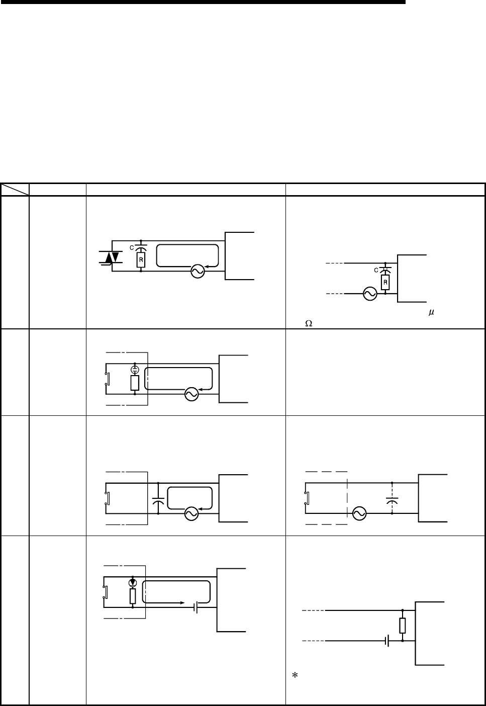
11 - 38 11 - 38
MELSEC-Q
11 TROUBLESHOOTING
11.5 I/O Module Troubleshooting
This chapter explains possible problems with I/O circuits and their corrective actions.
11.5.1 Input circuit troubleshooting
This section describes possible problems with input circuits and their corrective
actions.
Input Circuit Problems and Corrective Actions
Condition Cause Corrective Action
Example 1
Input signal
does not
turn OFF.
• Leakage current of input switch
(e.g. drive by non-contact switch).
Leakage
current Input module
AC input
Power supply
• Connect an appropriate resistor which will
make the voltage across the terminals of the
input module lower than the OFF voltage
value.
AC input
Input module
It is recommended to use 0.1 to 47 F + 47 to
120
(
1/2W
)
for the CR constant.
Example 2
Input signal
does not
turn OFF.
• Drive by a limit switch with neon lamp.
Leakage
current
AC input
Input module
Power supply
• Same as Example 1.
• Or make up another independent display
circuit.
Example 3
Input signal
does not
turn OFF.
• Leakage current due to line capacity of wiring
cable.
(Line capacity C of twisted pair wire is approx.
100 pF/m).
Leakage
current
AC input
Input module
Power supply
• Same as Example 1.
• However, leakage current is not generated
when the power supply is located in the input
equipment side as shown below.
AC input
Input module
Power supply
Example 4
Input signal
does not
turn OFF.
• Drive by switch with LED indicator.
Leakage
current
DC input
(plus common
)
Input module
• Connect a register which will make the voltage
between the input module terminal and
common lower than the OFF voltage, as
shown below.
DC input
(plus common
)
Input module
Resistor
A calculation example of a value for a
connected resistor is given on the following
page.
11 - 39 11 - 39
MELSEC-Q
11 TROUBLESHOOTING
Input Circuit Problems and Corrective Actions (Continued)
Condition Cause Corrective Action
Example 5
Input signal
does not
turn OFF.
• Sneak path due to the use of two power
supplies.
Input module
E1E2
>E2
E1
• Use only one power supply.
• Connect a sneak path prevention diode.
(Figure below)
Input module
E1E2
Example 6
False input
due to
noise
Depending on response time setting, noise is
imported as input.
Change response time setting.
Example : 1ms 5ms
(Setting of a shorter response time may produce
a higher effect on periodic excessive noise.)If no
effects are produced by the above, take basic
actions to prevent excessive noise form
entering, e.g. avoid bundling the power and I/O
cables, and suppress noise by adding surge
absorbers to such noise sources as relays and
conductors used with the same power supply.)
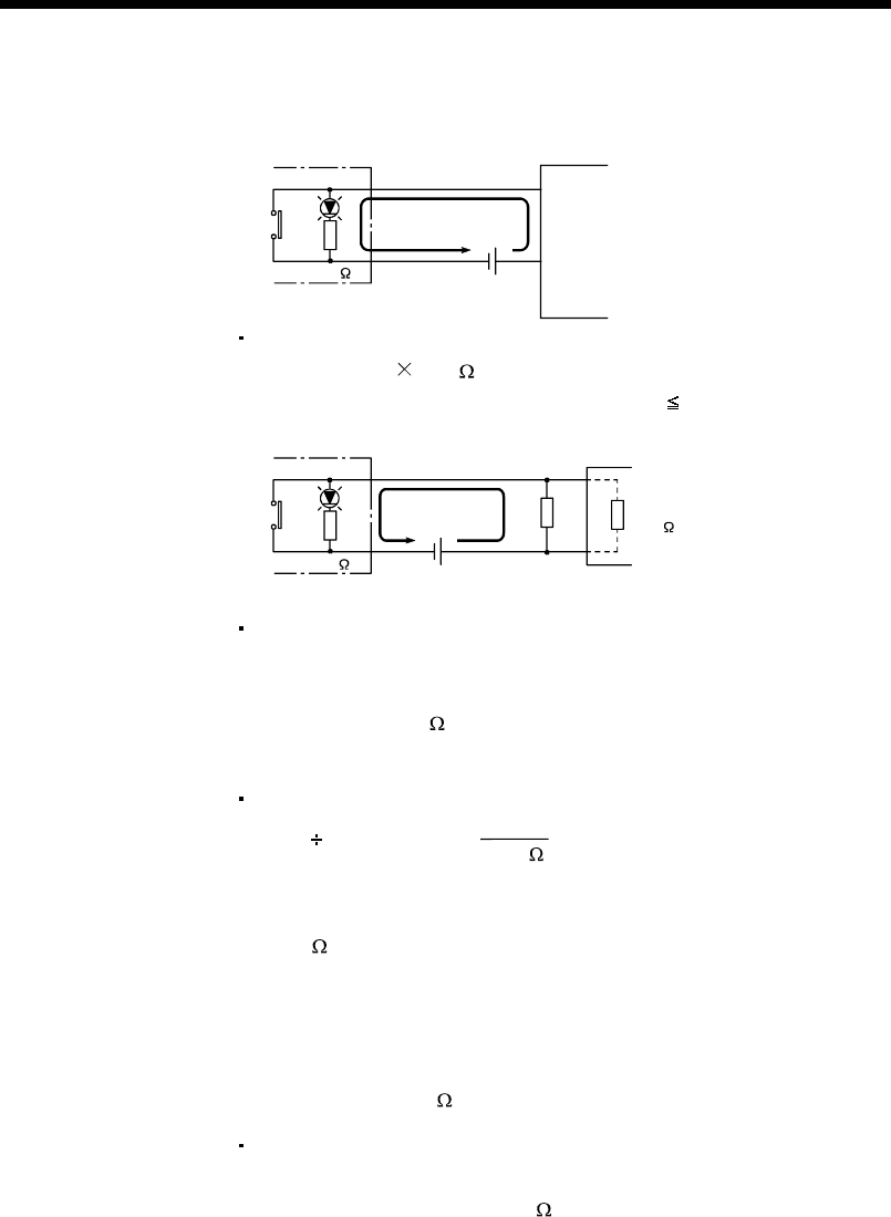
11 - 40 11 - 40
MELSEC-Q
11 TROUBLESHOOTING
<Calculation example of Example 4>
Leakage current
2.33mA
24VDC
Input module
QX40
If a switch with an LED display
is connected to QX40 and current
of 2.33 mA is leaked.
4.7k
Voltage VTB across the terminal and common base is:
VTB = 2.33[mA] 5.6[k ] = 13[V] (Ignore the voltage drop caused by the LED.)
Because the condition for the OFF voltage ( 11 [V]) is not satisfied, the input does
not turn off. To correct this, connect a resistor as shown below.
QX40
Current I
24VDC
Input impedance
R
4.7k
5.6k
Calculation of current for resistor R
The voltage of QX40 across the terminals must be reduced to 11 [V] or less.
The required current
(24-11[V]) ÷ 4.7[k ] = 2.77[mA]
Therefore resistor R of flowing current I of 2.77 [mA] or more must be connected.
Calculation of resistance of connected resistor R
11[V] R > 2.77[mA] - 5.6[k ]
11[V]
11[V] ÷ R > 2.77-1.96[mA]
11[V] ÷ 0.81[mA] > R
13.6[k ] > R
Resistance of the connected resistor R is obtained in the above equations.
Suppose that the resistance R is 12 [kW].
The power capacity W of the resistor during activation of the switch is:
W = (Applied voltage)2 / R
W = (28.8[V])2/12[k ]=0.069[W]
Because the resistance is selected so that the power capacity is three to five times
the actual power consumption, a third to a half [W] should be selected.
In this case, a resistor of 12 [k ] and a third to a half [W] should be connected across
the terminal and COM.
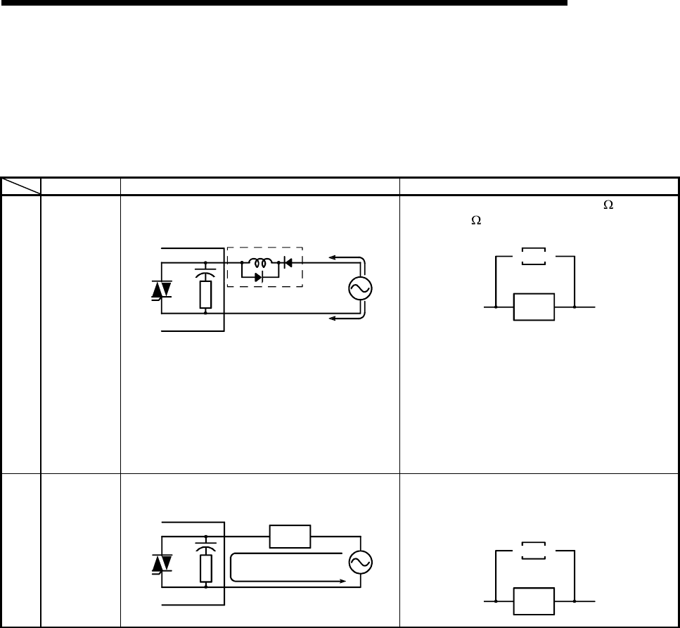
11 - 41 11 - 41
MELSEC-Q
11 TROUBLESHOOTING
11.5.2 Output Circuit Troubleshooting
This section explains trouble examples and troubleshooting methods in the output
circuit.
Output Circuit Troubleshooting
Condition Cause Corrective Action
Example 1
Excessive
voltage is
applied to
load when
output turns
off.
• When load is half-wave rectified inside
(This is typical of some solenoids.)
QY22 [1]
[2]
D1
C
Output module
Load
• When the polarity of the power supply is [1],
the capacitor C is charged. When the polarity
is [2], the voltage charged in C plus the power
supply voltage is applied to across D1. The
maximum value of the voltage is approx. 2.2E.
(This usage does not pose problems to the
output components but may deteriorate the
diode built in the load
,
causin
g
burnout
,
etc.
)
• Connect a resistor of several ten K to several
hundred K across the load.
Load
Resistor
Example 2
Load does
not turn off.
(Triac
output)
• Leakage current due to the built-in surge
suppressor
QY22
Output module Load
Leakage current
• Connect a resistor across the load.
(If the wiring from the output module to the
load is long, be careful since there may be a
leakage current due to the line capacity.)
Load
Resistor
11 - 42 11 - 42
MELSEC-Q
11 TROUBLESHOOTING
11.6 Special Relay List
Special relays, SM, are internal relays whose applications are fixed in the PLC.
For this reason, they cannot be used by sequence programs in the same way as the normal
internal relays.
However, they can be turned ON or OFF as needed in order to control the CPU module and
remote I/O modules.
The headings in the table that follows have the following meanings.
Item Function of Item
Number • Indicates the number of the special relay.
Name • Indicates the name of the special relay.
Meaning • Indicates the nature of the special relay.
Explanation • Contains detailed information about the nature of the special relay.
Set by (When set)
• Indicates whether the relay is set by the system or user, and, if it is set by the system, when
setting is performed.
<Set by>
S : Set by system
U : Set by user (in sequence program or test operation at a GX Developer)
S/U : Set by both system and user
<When set>
Indicated only if setting is done by system.
Each END : Set during each END processing
Initial : Set only during initial processing
(when power supply is turned ON, or when going from STOP to
RUN)
Status change : Set only when there is a change in status
Error : Set when error is generated
Instruction execution : Set when instruction is executed
Request : Set only when there is a user request
(through SM, etc.)
Corresponding ACPU
M9
• Indicates special relay M9 corresponding to the ACPU.
(Change and notation when there has been a change in contents)
• Items indicated as "New" have been newly added for High performance model
QCPU/QnACPU.
Corresponding CPU
• Indicates the corresponding CPU module type name.
+Rem: Can be applied to all CPU module types and MELSECNET/H remote I/O modules.
: Can be applied to all types of CPU module
QCPU: Can be applied to High Performance model QCPU
QnA: Can be applied to QnA series and Q2ASCPU Series
Remote: Can be applied to the MELSECNET/H remote I/O modules.
Each CPU type name: Can be applied only to the specific CPU module. (e.g. Q4ARCPU,
Q3ACPU)
For details on the following items, refer to the following manuals:
• Networks • For Q Corresponding MELSECNET/H Network System Reference Manual
(PLC to PLC network)
• For Q Corresponding MELSECNET/H Network System Reference Manual
(Remote I/O network)
• For QnA/Q4AR MELSECNET/10 Network System Reference Manual
• SFC QCPU(Q Mode)/QnACPU Programming Manual (SFC)
POINT
(1) SM1200 to SM1255 are used for QnACPU.
These relays are vacant with QCPU.
(2) Special relays SM1500 and later are dedicated for Q4ARCPU.
11 - 43 11 - 43
MELSEC-Q
11 TROUBLESHOOTING
Special Relay List
(1) Diagnostic Information
Number Name Meaning Explanation Set by
(When Set)
Corresponding
ACPU
M9
Applicable
CPU
SM0 Diagnostic errors
OFF : No error
ON : Error
• ON if diagnosis results show error occurrence
(Includes when an annunciator is ON, and when an error
is detected with CHK instruction)
• Stays ON subsequently even if normal operations
restored
S (Error) New
SM1 Self-diagnosis
error
OFF : No self-diagnosis
errors
ON : Self-diagnosis
• Comes ON when an error occurs as a result of self-
diagnosis. (Does not include when annunciator is ON or
when error is detected by CHK instruction.)
• Stays ON subsequently even if normal operations
restored
S (Error) M9008
SM5 Error common
information
OFF : No error common
information
ON : Error common
information
• When SM0 is ON, ON if there is error common
information S (Error) New
SM16 Error individual
information
OFF : No error common
information
ON : Error common
information
• When SM0 is ON, ON if there is error individual
information S (Error) New
SM50 Error reset OFF ON : Error reset • Conducts error reset operation U New
+Rem
SM51 Battery low latch OFF : Normal
ON : Battery low
• ON if battery voltage at CPU module or memory card
drops below rated value. Stays ON subsequently even
after normal operation is restored
• Synchronous with BAT. ALA/BAT. LED
S (Error) M9007
SM52 Battery low OFF : Normal
ON : Battery low
• Same as SM51, but goes OFF subsequently when
battery voltage returns to normal. S (Error) M9006
• Comes ON it a momentary power interruption of less
than 20ms occurred during use of the AC power supply
module, and reset by turning the power OFF, then ON.
• Comes ON if a momentary power interruption of less
than 10ms occurred during use of the DC power supply
module, and reset by turning power OFF, then ON.
QCPU
SM53 AC/DC DOWN
detection
OFF : AC/DC DOWN not
detected
ON : AC/DC DOWN
detected • Comes ON if a momentary power interruption of less
than 1ms occurred during use of the DC power supply
module, and reset by turning power OFF, then ON.
S (Error) M9005
QnA
SM54 MINI link errors OFF : Normal
ON : Error
• Goes ON if MINI (S3) link error is detected at even one of
the installed MELSECNET/MINI master modules.
Stays ON subsequently even after normal operation is
restored.
S (Error) M9004 QnA
SM56 Operation Errors
OFF : Normal
ON : Operation error
• ON when operation error is generated
• Stays ON subsequently even if normal operations
restored
S (Error) M9011
SM60 Blown fuse
detection
OFF : Normal
ON : Module with blown fuse
• Comes ON even if there is only one output module with a
blown fuse, and remains ON even after return to normal
• Blown fuse status is checked even for remote I/O station
output modules.
S (Error) M9000
SM61 I/O module
verification error
OFF : Normal
ON : Error
• Comes ON if there is a discrepancy between the actual
I/O modules and the registered information when the
power is turned on
• I/O module verification is also conducted for remote I/O
station modules.
S (Error) M9002
+Rem
SM62 Annunciator
detection
OFF : Not detected
ON : Detected • Goes ON if even one annunciator F goes ON.
S
(Instruction
execution)
M9009
SM80 CHK detection OFF : Not detected
ON : Detected
• Goes ON if error is detected by CHK instruction.
• Stays ON subsequently even after normal operation is
restored.
S
(Instruction
execution)
New
SM90 Corresponds to SD90 M9108
SM91 Corresponds to SD91 M9109
SM92 Corresponds to SD92 M9110
SM93 Corresponds to SD93 M9111
SM94 Corresponds to SD94 M9112
SM95 Corresponds to SD95 M9113
SM96 Corresponds to SD96 M9114
SM97 Corresponds to SD97 New
SM98 Corresponds to SD98 New
SM99
Startup of
watchdog timer
for step transition
(Enabled only
when SFC
program exists)
OFF : Not started
(watchdog timer reset)
ON : Started
(watchdog timer
started)
Corresponds to SD99
• Goes ON when measurement of
step transition watchdog timer is
commenced.
• Resets watchdog timer when it
goes OFF.
U
New
11 - 44 11 - 44
MELSEC-Q
11 TROUBLESHOOTING
Special Relay List
(2) System information
Number Name Meaning Explanation Set by
(When Set)
Corresponding
ACPU
M9
Applicable
CPU
SM202 LED OFF
command OFF ON : LED OFF • When this relay goes from OFF to ON, the LEDs
corresponding to the individual bits at SD202 go off U New
SM203 STOP contact STOP status • Goes ON at STOP status S (Status
change) M9042
SM204 PAUSE contact PAUSE status • Goes ON at PAUSE status S (Status
change) M9041
SM205 STEP-RUN
contact STEP-RUN status • Goes ON at STEP-RUN status S (Status
change) M9054
PAUSE enable
coil
OFF : PAUSE disabled
ON : PAUSE enabled
• PAUSE status is entered if this relay is ON when the
remote PAUSE contact goes ON U M9040
SM206 Device test
request
acceptance
status
OFF : Device test not yet
executed
ON : Device test executed
• Comes ON when the device test mode is executed on
GX Developer. S (Request) New Remote
SM210 Clock data set
request
OFF : Ignored
ON : Set request
• When this relay goes from OFF to ON, clock data being
stored from SD210 to SD213 after execution of END
instruction for changed scan is written to the clock device.
U M9025
SM211 Clock data error OFF : No error
ON : Error
• ON when error is generated in clock data (SD210 to
SD213) value, and OFF if no error is detected. S (Request) M9026
SM212 Clock data
display
OFF : Ignored
ON : Display
• Displays clock data as month, day, hour, minute, and
second at the LED display at front of CPU module. U M9027
Q3A
Q4A
Q4AR
SM213 Clock data read
request
OFF : Ignored
ON : Read request
• When this relay is ON, clock data is read to SD210 to
SD213 as BCD values. U M9028
+Rem
SM240 No. 1 CPU reset
flag OFF : PLC No. 1 reset cancel
ON : PLC No. 1 resetting
• Goes OFF when reset of the PLC No. 1 is canceled.
• Comes ON when the PLC No. 1 is resetting (including
the case where the PLC is removed from the base unit).
The other PLCs are also put in reset status.
SM241 No. 2 CPU reset
flag
OFF : PLC No. 2 reset cancel
ON : PLC No. 2 resetting
• Goes OFF when reset of the PLC No. 2 is canceled.
• Comes ON when the PLC No. 2 is resetting (including
the case where the PLC is removed from the base unit).
The other PLCs result in "MULTI CPU DOWN" (error
code: 7000).
SM242 No. 3 CPU reset
flag
OFF : PLC No. 3 reset cancel
ON : PLC No. 3 resetting
• Goes OFF when reset of the PLC No. 3 is canceled.
• Comes ON when the PLC No. 3 is resetting (including
the case where the PLC is removed from the base unit).
The other PLCs result in "MULTI CPU DOWN" (error
code: 7000).
SM243 No. 4 CPU reset
flag
OFF : PLC No. 4 reset cancel
ON : PLC No. 4 resetting
• Goes OFF when reset of the PLC No. 4 is canceled.
• Comes ON when the PLC No. 4 is resetting (including
the case where the PLC is removed from the base unit).
The other PLCs result in "MULTI CPU DOWN" (error
code: 7000).
SM244 No. 1 CPU error
flag
OFF : PLC No. 1 normal
ON : PLC No. 1 during stop
error
• Goes OFF when the PLC No. 1 is normal (including a
continuation error).
• Comes ON when the PLC No. 1 is during a stop error.
SM245 No. 2 CPU error
flag
OFF : PLC No. 2 normal
ON : PLC No. 2 during stop
error
• Goes OFF when the PLC No. 2 is normal (including a
continuation error).
• Comes ON when the PLC No. 2 is during a stop error.
SM246 No. 3 CPU error
flag
OFF : PLC No. 3 normal
ON : PLC No. 3 during stop
error
• Goes OFF when the PLC No. 3 is normal (including a
continuation error).
• Comes ON when the PLC No. 3 is during a stop error.
SM247 No. 4 CPU error
flag
OFF : PLC No. 4 normal
ON : PLC No. 4 during stop
error
• Goes OFF when the PLC No. 4 is normal (including a
continuation error).
• Comes ON when the PLC No. 4 is during a stop error.
S (Status
change) New
QCPU
function
Ver. B
11 - 45 11 - 45
MELSEC-Q
11 TROUBLESHOOTING
Special Relay List (Continued)
Number Name Meaning Explanation Set by
(When Set)
Corresponding
ACPU
M9
Applicable
CPU
SM250 Max. loaded I/O
read
OFF : Ignored
ON : Read
• When this relay goes from OFF to ON, maximum loaded
I/O number is read to SD250. U New
+Rem
SM251 I/O change flag OFF : No replacement
ON : Replacement
• After the head I/O number of the I/O module being
replaced is set in SD251 is set, on-line I/O module
replace ment is enabled when this relay is ON.
(Only one module can be replaced at each setting.)
• To replace an I/O module in the RUN status, use the
program or a peripheral device to turn this relay ON; to
replace an I/O module in the STOP status, turn this relay
ON in the test mode of a peripheral device.
• Do not switch between RUN and STOP status until I/O
module replacement is completed.
U (END) M9094
SM252 I/O change OK OFF : Replacement prohibited
ON : Replacement enabled • Goes ON when I/O replacement is OK. S (END) New
Q2A (S1)
Q3A
Q4A
Q4AR
SM254 All stations
refresh command
OFF : Refresh arrival station
ON : Refresh all stations
• Effective for the batch refresh
(also effective for the low speed cyclic)
• Designate whether to receive arrival stations only or to
receive all slave stations.
U (Every
END) New QCPU
SM255 OFF : Operative network
ON : Standby network
• Goes ON for standby network
(If no designation has been made concerning active or
standby, active is assumed.)
S (Initial) New
SM256 OFF : Reads
ON : Does not read
• For refresh from link to CPU (B, W, etc.) indicate whether
to read from the link module. U New
SM257
MELSECNET/10
module 1
information
OFF : W rites
ON : Does not write
• For refresh from CPU to link (B, W, etc.), designate
whether to write to the link module. U New
SM260 OFF : Operative network
ON : Standby network
• Goes ON for standby network
(If no designation has been made concerning active or
standby, active is assumed.)
S (Initial) New
SM261 OFF : Reads
ON : Does not read
• For refresh from link to CPU (B, W, etc.) indicate whether
to read from the link module. U New
SM262
MELSECNET/10
module 2
information
OFF : W rites
ON : Does not write
• For refresh from CPU to link (B, W, etc.), designate
whether to write to the link module. U New
SM265 OFF : Operative network
ON : Standby network
• Goes ON for standby network
(If no designation has been made concerning active or
standby, active is assumed.)
S (Initial) New
SM266 OFF : Reads
ON : Does not read
• For refresh from link to CPU (B, W, etc.) indicate whether
to read from the link module. U New
SM267
MELSECNET/10
module 3
information
OFF : W rites
ON : Does not write
• For refresh from CPU to link (B, W, etc.), designate
whether to write to the link module. U New
SM270 OFF : Operative network
ON : Standby network
• Goes ON for standby network
(If no designation has been made concerning active or
standby, active is assumed.)
S (Initial) New
SM271 OFF : Reads
ON : Does not read
• For refresh from link to CPU (B, W, etc.) indicate whether
to read from the link module. U New
SM272
MELSECNET/10
module 4
information
OFF : W rites
ON : Does not write
• For refresh from CPU to link (B, W, etc.), designate
whether to write to the link module. U New
• Goes ON when a CC-Link error is detected in any of the
installed QJ61QBT11.
Goes OFF when normal operation is restored.
S (Status
change) New QCPU
Remote
SM280 CC-Link error OFF : Normal
ON : Error • Goes ON when a CC-Link error is detected in any of the
installed A(1S)J61QBT11.
Stays ON even after normal operation is restored.
S (Error) New QnA
SM320
Presence/absenc
e of SFC
program
OFF : SFC program absent
ON : SFC program present
• ON if SFC program is correctly registered, and OFF if not
registered.
• Goes OFF if SFC dedicated instruction is not correct.
S (Initial) M9100
SM321 Start/stop SFC
program
OFF : SFC program stop
ON : SFC program start
• Initial value is set at the same value as SM320.
(Goes ON automatically if SFC program is present.)
• SFC program will not execute if this goes OFF prior to
SFC program processing
• Starts SFC program when this relay goes from OFF to
ON.
• Stops SFC program when this relay goes from ON to
OFF.
S (Initial)
U
M9101
format change
11 - 46 11 - 46
MELSEC-Q
11 TROUBLESHOOTING
Special Relay List (Continued)
Number Name Meaning Explanation Set by
(When Set)
Corresponding
ACPU
M9
Applicable
CPU
SM322 SFC program
start status
OFF : Initial start
ON : Restart
• Initial value is set at ON or OFF depending on
parameters.
• When this relay is OFF, all execution status are cleared
from time SFC program was stopped; starts from the
initial step of block where the start request was made.
• When this relay is ON, starts from execution block and
execution step active at time SFC program was stopped.
(ON is enabled only when resumptive start has been
designated at parameters.)
• SM902 is not automatically designated for latch.
S (Initial)
U
M9102
format change
SM323
Presence/absenc
e of continuous
transition for
entire block
OFF : Continuous transition
not effective
ON : Continuous transition
effective
• When this relay is OFF, transition occurs at one scan/one
step, for all blocks.
• When this relay is ON, transition occurs continuously for
all blocks in one scan.
• In designation of individual blocks, priority is given to the
continuous transition bit of the block.
(Designation is checked when block starts.)
U M9103
SM324
Continuous
transition
prevention flag
OFF : When transition is
executed
ON : When no transition
• When continuous transition is effective, goes ON when
continuous transition is not being executed; goes OFF
when continuous transition is being executed.
• Normally ON when continuous transition is not effective.
S
(Instruction
execution)
M9104
SM325 Output mode at
block stop
OFF : OFF
ON : Preserves
When block stops, selects active step operation output.
• All coil outputs go OFF when this relay is OFF.
• Coil outputs are preserved when this relay is ON.
S (Initial)
U M9196
SM326 SFC device clear
mode
OFF : Clear device
ON : Preserves device
Selects the device status when the stopped CPU is run
after the sequence program or SFC program has been
modified when the SFC program exists.
U New
SM327
Output during
end step
execution
OFF : OFF
ON : Preserves
Selects the output action of the step being held when a
block is ended by executing the end step.
• All coil outputs go OFF when this relay is OFF.
• Coil outputs are preserved when this relay is ON.
S (Initial)
U New
SM330
Operation mode
for low speed
execution type
program
OFF : Asynchronous mode
ON : Synchronous mode
Low speed execution type program ON for 1 scan only
after RUN U (END) New
SM390 Access execution
flag
When ON, access to the
intelligent function module is
completed
• Stores the status of the intelligent function module access
instruction executed immediately before.
(This information will be overwritten when the intelligent
function module access instruction is executed again.)
• This flag is used by the user in a program as the
completion bit.
S (Status
change) New QCPU
11 - 47 11 - 47
MELSEC-Q
11 TROUBLESHOOTING
Special Relay List
(3) System clocks/counters
Number Name Meaning Explanation Set by
(When Set)
Corresponding
ACPU
M9
Applicable
CPU
SM400 Always ON
O
N
O
FF • Normally is ON S
(Every END
processing)
M9036
SM401 Always OFF
O
N
O
FF • Normally is OFF S
(Every END
processing) M9037
SM402 ON for 1 scan
only after RUN
O
N
O
FF 1 scan
• After RUN, ON for 1 scan only.
• This connection can be used for scan execution type
programs only.
S
(Every END
processing) M9038
SM403 After RUN, OFF
for 1 scan only ON
OFF 1 scan
• After RUN, OFF for 1 scan only.
• This connection can be used for scan execution type
programs only.
S
(Every END
processing) M9039
SM404
Low speed
execution type
program
ON for 1 scan
only after RUN
O
N
O
FF 1 scan
• After RUN, ON for 1 scan only.
• This connection can be used for low speed execution
type programs only.
S
(Every END
processing) New
SM405
Low speed
execution type
program
After RUN, OFF
for 1 scan only
ON
OFF 1 scan
• After RUN, OFF for 1 scan only.
• This connection can be used for low speed execution
type programs only.
S
(Every END
processing) New
SM409 0.01 second
clock 0.005 sec.
0.005 sec.
• Repeatedly changes between ON and OFF at 5-ms
interval.
• When PLC power supply is turned OFF or a CPU module
reset is performed, goes from OFF to start.
• Note that the ON-OFF status changes when the
designated time has elapsed during the execution of the
program.
S (Status
change) New QCPU
SM410 0.1 second clock 0.05 sec.
0.05 sec.
M9030
SM411 0.2 second clock 0.1sec.
0.1sec.
M9031
SM412 1 second clock 0.5 sec.
0.5 sec.
M9032
SM413 2 second clock 1 sec.
1 sec.
• Repeatedly changes between ON and OFF at each
designated time interval.
• When PLC power supply is turned OFF or a CPU module
reset is performed, goes from OFF to start.
• Note that the ON-OFF status changes when the
designated time has elapsed during the execution of the
program.
S (Status
change)
M9033
SM414 2n second clock n sec.
n sec.
• Goes between ON and OFF in accordance with the
number of seconds designated by SD414.
• When PLC power supply is turned OFF or a CPU module
reset is performed, goes from OFF to start.
• Note that the ON-OFF status changes when the
designated time has elapsed during the execution of the
program.
S (Status
change) M9034 format
change
SM415 2n (ms) clock n(ms)
n(ms)
• Switches between ON and OFF in accordance with the
number of milliseconds designated by SD415.
• When PLC power supply is turned OFF or a CPU module
reset is performed, goes from OFF to start.
• Note that the ON-OFF status changes when the
designated time has elapsed during the execution of the
program.
S (Status
change) New QCPU
SM420 User timing clock
No.0 M9020
SM421 User timing clock
No.1 M9021
SM422 User timing clock
No.2 M9022
SM423 User timing clock
No.3 M9023
SM424 User timing clock
No.4
• Relay repeats ON/OFF switching at fixed scan intervals.
• When PLC power supply is turned OFF or a CPU module
reset is performed, goes from OFF to start.
• The ON/OFF intervals are set with the DUTY instruction.
DUTY n1 n2 SM420
S
(Every END
processing)
M9024
SM430 User timing clock
No.5
SM431 User timing clock
No.6
SM432 User timing clock
No.7
SM433 User timing clock
No.8
SM434 User timing clock
No.9
n2
scan
n2
scan
n1
scan
• For use with SM420 to SM424 low speed programs. S
(Every END
processing) New
11 - 48 11 - 48
MELSEC-Q
11 TROUBLESHOOTING
Special Relay List
(4) Scan information
Number Name Meaning Explanation Set by
(When Set)
Corresponding
ACPU
M9
Applicable
CPU
SM510
Low speed
program
execution flag
OFF : Completed or not
executed
ON : Execution under way.
• Goes ON when low speed execution type program is
executed.
S
(Every END
processing)
New
SM551 Reads module
service interval
OFF : Ignored
ON : Read
• When this relay goes from OFF to ON, the module
service interval designated by SD550 is read to SD551 to
SD552.
U New
+Rem
(5) Memory cards
Number Name Meaning Explanation Set by
(When Set)
Corresponding
ACPU
M9
Applicable
CPU
SM600 Memory card
usable flags
OFF : Unusable
ON : Use enabled • ON when memory card is ready for use by user S (Initial) New
SM601 Memory card
protect flag
OFF : No protect
ON : Protect • Goes ON when memory card protect switch is ON S (Initial) New
SM602 Drive 1 flag OFF : No drive 1
ON : Drive 1 present • Goes ON when loaded memory card is RAM. S (Initial) New
SM603 Drive 2 flag OFF : No drive 2
ON : Drive 2 present • Goes ON when loaded memory card is ROM. S (Initial) New
SM604 Memory card
in-use flag
OFF : Not used
ON : In use • Goes ON when memory card is in use S (Initial) New
SM605
Memory card
remove/insert
prohibit flag
OFF : Remove/insert enabled
ON : Remove/insert
prohibited
• Goes ON when memory card cannot be inserted or
removed U New
SM609
Memory card
remove/insert
enable flag
OFF : Remove/insert
prohibited
ON : Remove/insert enabled
• Turned ON by user to enable the removal/insertion of
memory card.
• Turned OFF by the system after the memory card is
removed.
U/S New
• Always ON S (Initial) New QCPU
SM620 Memory card B
usable flags
OFF : Unusable
ON : Use enabled • ON when memory card B is ready for use by user S (Initial) New
Q2A (S1)
Q3A
Q4A
Q4AR
• Always ON S (Initial) New QCPU
SM621 Memory card B
protect flag
OFF : No protect
ON : Protect • Goes ON when memory card B protect switch is ON S (Initial) New
Q2A (S1)
Q3A
Q4A
Q4AR
• Always ON S (Initial) New QCPU
SM622 Drive 3 flag OFF : No drive 3
ON : Drive 3 present • Goes ON when drive 3 (card 2 RAM area) is present S (Initial) New
Q2A (S1)
Q3A
Q4A
Q4AR
• Always ON S (Initial) New QCPU
SM623 Drive 4 flag OFF : No drive 4
ON : Drive 4 present • Goes ON when drive 4 (card 2 ROM area) is present S (Initial) New
SM624 Memory card B
in-use flag
OFF : Not used
ON : In use • Goes ON when memory card B is in use S (Initial) New
SM625
Memory card B
remove/insert
prohibit flag
OFF : Remove/insert enabled
ON : Remove/insert
prohibited
• Goes ON when memory card B cannot be inserted or
removed U New
Q2A (S1)
Q3A
Q4A
Q4AR
SM640 File register use OFF : File register not used
ON : File register in use • Goes ON when file register is in use S (Status
change) New
SM650 Comment use OFF : File register not used
ON : File register in use • Goes ON when comment file is in use S (Status
change) New
SM660 Boot operation
OFF : Internal memory
execution
ON : Boot operation in
progress
• Goes ON while boot operation is in process
• Goes OFF if boot designation switch is OFF
S (Status
change) New
SM672
Memory card A
file register
access range flag
OFF : Within access range
ON : Outside access range
• Goes ON when access is made to area outside the range
of file register R of memory card A
(Set within END processing.)
• Reset at user program
S/U New
11 - 49 11 - 49
MELSEC-Q
11 TROUBLESHOOTING
Special Relay List (Continued)
Number Name Meaning Explanation Set by
(When Set)
Corresponding
ACPU
M9
Applicable
CPU
SM673
Memory card B
file register
access range flag
OFF : Within access range
ON : Outside access range
• Goes ON when access is made outside the range of file
registers, R. of memory card B.
(Set within END processing.)
• Reset at user program
S/U New
Q2A (S1)
Q3A
Q4A
Q4AR
(6) Instruction-Related Special Relays
Number Name Meaning Explanation Set by
(When Set)
Corresponding
ACPU
M9
Applicable
CPU
SM700 Carry flag OFF : Carry OFF
ON : Carry ON • Carry flag used in application instruction
S
(Instruction
execution)
M9012
SM701
Number of output
characters
selection
OFF : 16 characters output
ON : Outputs until NUL
• When SM701 is OFF, 16 characters of ASCII code are
output.
• When SM701 is ON, output conducted until NUL (00H)
code of ASCII code is encountered.
U M9049
SM702 Search method OFF : Search next
ON : 2-part search
• Designates method to be used by search instruction.
• Data must be arranged for 2-part search. U New
SM703 Sort order OFF : Ascending order
ON : Descending order
• The sort instruction is used to designate whether data
should be sorted in ascending order or in descending
order.
U New
SM704 Block comparison
OFF : Non-match found
ON : All match
• Goes ON when all data conditions have been met for the
BKCMP instruction.
S
(Instruction
execution)
New
SM707
Selection of real
number
instruction
processing type
OFF : Speed oriented
ON : Accuracy oriented
• When SM707 is OFF, real number instructions are
processed at high speed.
• When it is ON, real number instructions are processed
with high accuracy.
U New Q4AR
SM710
CHK instruction
priority ranking
flag
OFF : Conditions priority
ON : Pattern priority
• Remains as originally set when OFF.
• CHK priorities updated when ON.
S
(Instruction
execution)
New
SM711
Divided
transmission
status
OFF : Other than during
divided processing
ON : During divided
processing
• In processing of AD57(S1), goes ON when screen is split
for transfer, and goes OFF when split processing is
completed
S
(Instruction
execution)
M9065
SM712
Transmission
processing
selection
OFF : Batch processing
ON : Divided processing
• In processing of AD57(S1), goes ON when canvas
screen is divided for transfer.
S
(Instruction
execution)
M9066
SM714
Communication
request
registration area
BUSY signal
OFF : Communication
request to remote
terminal module
enabled
ON : Communication
request to remote
terminal module
disabled
• Used to determine whether communications requests to
remote terminal modules connected to the AJ71PT32-S3
can be executed or not.
S
(Instruction
execution)
M9081
QnA
SM715 EI flag OFF : During DI
ON : During EI • ON when EI instruction is being executed.
S
(Instruction
execution)
New
SM720 Comment read
completion flag
OFF : Comment read not
completed
ON : Comment read
completed
• Switches ON for only one scan when COMRD or PRC
instruction is completed.
S (Status
change) New
SM721 File being
accessed
OFF : File not accessed
ON : File being accessed
• Switches ON while a file is being accessed by the
S.FWRITE, S.FREAD, COMRD, PRC, or LEDC
instruction.
S (Status
change) New
SM722
BIN/DBIN
instruction error
disabling flag
OFF : Error detection
performed
ON : Error detection not
performed
• Turned ON when "OPERATION ERROR" is suppressed
for BIN or DBIN instruction. U New
QCPU
SM730
BUSY signal for
CC-Link
communication
request
registration area
OFF : Request for
communication with
intelligent device
station enabled
ON : Request for
communication with
intelligent device
station disabled
• Used for determination whether to enable or disable the
communication request for the intelligent device station
connected with A(1S)J61QBT11.
S
(Instruction
execution)
New QnA
11 - 50 11 - 50
MELSEC-Q
11 TROUBLESHOOTING
Special Relay List (Continued)
Number Name Meaning Explanation Set by
(When Set)
Corresponding
ACPU
M9
Applicable
CPU
SM736
PKEY instruction
execution in
progress flag
OFF : Instruction not
executed
ON : Instruction execution
• ON when PKEY instruction is being executed.
Goes OFF when CR is input, or when input character
string reaches 32 characters.
S
(Instruction
execution)
New
SM737
Keyboard input
reception flag for
PKEY instruction
OFF : Keyboard input
reception enabled
ON : Keyboard input
reception disabled
• Goes ON when keyboard input is being conducted.
Goes when keyboard input has been stored at the CPU.
S
(Instruction
execution)
New
SM738 MSG instruction
reception flag
OFF : Instruction not
executed
ON : Instruction execution
• Goes ON when MSG instruction is executed.
S
(Instruction
execution)
New
SM774 PID bumpless
processing
OFF : Forces match
ON : Does not force match
• In manual mode, designates whether or not to force the
SV value to match the PV value. U New
OFF : Performs link refresh
ON : Performs no link
refresh
• Selects whether only the general data process is
performed for the execution of the COM instruction or the
link refresh process is also performed.
U New
SM775
Selection of link
refresh
processing during
COM instruction
execution
OFF : Performs all refresh
processes
ON : Performs the refresh
set the SD778
• Selects whether all refresh process or the refresh set with
SD778 is performed when COM instruction is executed. U New
QCPU
serial
number **
or later
SM776
Enable/disable
local device at
CALL
OFF : Local device disabled
ON : Local device enabled
• Determines whether to enable/disable the local device in
the program CALLED at CALL.
U (Status
change) New
SM777
Enable/disable
local device in
interrupt program
OFF : Local device disabled
ON : Local device enabled
• Determines whether to enable/disable the local device at
the execution of interrupt programs.
U (Status
change) New
SM780
CC-Link
dedicated
instruction
executable
OFF : CC-Link dedicated
instruction executable
ON : CC-Link dedicated
instruction not
executable
• Switches ON when the number of the CC-Link dedicated
instructions that can be executed simultaneously reaches
32. Switches OFF when the number goes below 32.
U (Status
change) New QnA
(7) Debug
Number Name Meaning Explanation Set by
(When Set)
Corresponding
ACPU
M9
Applicable
CPU
Trace preparation • Switches ON when the trace preparation is completed. S (Status
change) New QCPU
SM800 Sampling trace
preparation
OFF : Not ready
ON : Ready • Goes ON when sampling trace is ready S (Status
change) New QnA
Trace start • Trace started when this goes ON.
• Suspended when OFF (Related special M all OFF) U M9047 QCPU
SM801 Sampling trace
start
OFF : Suspend
ON : Start • Sampling trace started when this goes ON
• Suspended when OFF (Related special M all OFF) U M9047 QnA
Trace execution
in progress • Switches ON during execution of trace. S (Status
change) M9046 QCPU
SM802 Sampling trace
execution in
progress
OFF : Suspend
ON : Start • Goes ON during execution of sampling trace S (Status
change) M9046 QnA
Trace trigger • Trace is triggered when this relay switches from OFF to
ON. (Identical to TRACE instruction execution status) U M9044 QCPU
SM803 Sampling trace
trigger
OFF ON: Start • Sampling trace trigger goes ON when this goes from
OFF to ON (Identical to STRA instruction execution
status)
U M9044 QnA
After trace trigger • Switches ON after trace is triggered. S (Status
change) New QCPU
SM804 After sampling
trace trigger
OFF : Not after trigger
ON : After trigger • Goes ON after sampling trace trigger S (Status
change) New QnA
Trace completed • Switches ON at completion of trace. S (Status
change) 9043 QCPU
SM805 Sampling trace
completed
OFF : Not completed
ON : End • Goes ON at completion of sampling trace S (Status
change) 9043 QnA
11 - 51 11 - 51
MELSEC-Q
11 TROUBLESHOOTING
Special Relay List (Continued)
Number Name Meaning Explanation Set by
(When Set)
Corresponding
ACPU
M9
Applicable
CPU
SM806 Status latch
preparation
OFF : Not ready
ON : Ready • Goes ON when status latch is ready S (Status
change) New
SM807 Status latch
command OFF ON: Latch • Runs status latch command U New
SM808 Status latch
completion
OFF : Latch not completed
ON : Latch completed • Comes ON when status latch is completed. S (Status
change) 9055
SM809 Status latch clear OFF ON: Clear • Enable next status latch U New
QnA
SM810 Program trace
preparation
OFF : Not ready
ON : Ready • Goes ON when program trace is ready S (Status
change) New
SM811 Start program
trace
OFF : Suspend
ON : Start
• Program trace started when this goes ON
• Suspended when OFF (Related special M all OFF)
S (Status
change) New
SM812
Program trace
execution under
way
OFF : Suspend
ON : Start • ON when program trace execution is underway U New
SM813 Program trace
trigger OFF ON: Start • Program trace trigger goes ON when this goes from OFF
to ON (Identical to PTRA instruction execution status)
S (Status
change) New
SM814 After program
trace trigger
OFF : Not after trigger
ON : After trigger • Goes ON after program trace trigger S (Status
change) New
SM815 Program trace
completion
OFF : Not completed
ON : End • Goes ON at completion of program trace S (Status
change) New
QnA
SM820 Step trace
preparation
OFF : Not ready
ON : Ready • Goes ON after program trace registration, at ready. U New
SM821 Step trace starts OFF : Suspend
ON : Start
• When this goes ON, step trace is started
• Suspended when OFF (Related special M all OFF)
S (Status
change)
M9182 format
change
SM822
Step trace
execution
underway
OFF : Suspend
ON : Start
• Goes ON when step trace execution is underway
• Goes OFF at completion or suspension
S (Status
change) M9181
SM823 After step trace
trigger
OFF : Not after trigger
ON : Is after first trigger
• Goes ON if even 1 block within the step trace being
executed is triggered.
• Goes OFF when step trace is commenced.
S (Status
change) New
SM824 After Step trace
trigger
OFF : Is not after all triggers
ON : Is after all triggers
• Goes ON if all blocks within the step trace being
executed are triggered.
• Goes OFF when step trace is commenced.
S (Status
change) New
SM825 Step
tracecompleted
OFF : Not completed
ON : End
• Goes ON at step trace completion.
• Goes OFF when step trace is commenced.
S (Status
change) M9180
Trace error • Switches ON if error occurs during execution of trace. S (Status
change) New QCPU
SM826 Sampling trace
error
OFF : Normal
ON : Errors • Goes ON if error occurs during execution of sampling
trace.
S (Status
change) New
SM827 Status latch error OFF : Normal
ON : Errors • Goes ON if error occurs during execution of status latch. S (Status
change) New
SM828 Program trace
error
OFF : Normal
ON : Errors
• Goes ON if error occurs during execution of program
trace.
S (Status
change) New
QnA
(8) Latch area
Number Name Meaning Explanation Set by
(When Set)
Corresponding
ACPU
M9
Applicable
CPU
SM900 Power cut file OFF : No power cut file
ON : Power cut file present
• Goes ON if a file is present during access when power is
interrupted.
S/U (Status
change) New QnA
SM910 RKEY
registration flag
OFF : Keyboard input
notregistered
ON : Keyboard input
registered
• Goes ON at registration of keyboard input.
OFF if keyboard input is not registered.
S
(Instruction
execution)
New
11 - 52 11 - 52
MELSEC-Q
11 TROUBLESHOOTING
(9) A to Q/QnA conversion correspondences
Special relays SM1000 to SM1255 are the relays which correspond to ACPU special relays
M9000 to M9255 after A to Q/QnA conversion.
All of these special relays are controlled by the system so that users cannot turn them ON/OFF
in the program.
If users want to turn these relays ON/OFF, the program should be modified to use
QCPU/QnACPU special relays.
For SM1084 and SM1200 through SM1255, however, if a user can turn ON/OFF some of
special relays M9084 and M9200 through M9255 before conversion, the user can also turn
ON/OFF the corresponding relays among SM1084 and SM1200 through SM1255 after the
conversion.
For details on the ACPU special relays, see the user's manuals for the individual CPUs, and
MELSECNET or MELSECNET/B Data Link System Reference Manuals.
POINT
The processing time may be longer when converted special relays are used with QCPU.
Uncheck "A-series CPU compatibility setting" within the PC system setting in GX Developer
PC parameters when converted special relays are not used.
REMARK
The following are additional explanations about the Special Relay for Modification column.
1 When a special relay for modification is provided, the device number should be changed to
the provided QCPU/QnACPU special relay.
2 When is provided, the converted special relay can be used for the device number.
3 When is provided, the device number does not work with QCPU/QnACPU.
Special Relay List
ACPU
Special
Relay
Special
Relay after
Conversion
Special
Relay for
Modification Name Meaning Details Applicable
CPU
M9000 SM1000 Fuse blown OFF : Normal
ON : Module with blown fuse
• Turned on when there is one or more output units of
which fuse has been blown.Remains on if normal status
is restored.
Output modules of remote I/O stations are also checked
fore fuse condition.
M9002 SM1002 I/O module
verification error
OFF : Normal
ON : Error
• Turned on if the status of I/O module is different form
entered status when power is turned on.
Remains on if normal status is restored.
I/O module verification is done also to remote I/O station
modules.
(Reset is enabled only when special registers SD1116 to
SD1123 are reset.)
M9004 SM1004 NIMI link error OFF : Normal
ON : Error
• Turned on when the MINI(S3) link error is detected on
even one of the MELSECNET/MINI master modules
being loaded.Remains on if normal status is restored.
QnA
• Comes ON it a momentary power interruption of less
than 20ms occurred during use of the AC power supply
module, and reset by turning power OFF, then ON.
• Comes ON if a momentary power interruption of less
than 10ms occurred during use of the DC power supply
module, and reset by turning power OFF, then ON.
M9005 SM1005 AC DOWN
detection
OFF : AC DOWN not detected
ON : AC DOWN detected
• Comes ON if a momentary power interruption of less
than 1ms occurred during use of the DC power supply
module, and reset by turning power OFF, then ON.
11 - 53 11 - 53
MELSEC-Q
11 TROUBLESHOOTING
Special Relay List (Continued)
ACPU
Special
Relay
Special
Relay after
Conversion
Special
Relay for
Modification Name Meaning Details Applicable
CPU
M9006 SM1006 Battery low OFF : Normal
ON : Battery low
• Turned on when battery voltage reduces to less than
specified. Turned off when battery voltage becomes
normal.
M9007 SM1007 Battery low latch OFF : Normal
ON : Battery low
• Turned on when battery voltage reduces to less than
specified. Remains on if battery voltage becomes normal.
M9008 SM1008 SM1 Self-diagnosis
error
OFF : No error
ON : Error
• Turned on when error is found as a result of self-
diagnosis.
M9009 SM1009 SM62 Annunciator
detection
OFF : No F number detected
ON : F number detected • Turned on when OUT F of SET F instruction is executed.
Switched off when SD1124 data is zeroed.
M9011 SM1011 SM56 Operation error
flag
OFF : No error
ON : Error
• Turned on when operation error occurs during execution
of application instruction. Remains on if normal status is
restored.
M9012 SM1012 SM700 Carry flag OFF : Carry OFF
ON : Carry ON • Carry flag used in application instruction.
M9016 SM1016 Data memory
clear flag
OFF : lgnored
ON : Output claered
• Clears the data memory including the latch range (other
than special relays and special registers) in remote run
mode from computer, etc. when SM1016 is on.
M9017 SM1017 Data memory
clear flag
OFF : lgnored
ON : Output claered
• Clears the unlatched data memory (other than special
relays and registers) in remote run mode from computer,
etc. when SM1017 is on.
M9020 SM1020 User timing clock
No.0
M9021 SM1021 User timing clock
No.1
M9022 SM1022 User timing clock
No.2
M9023 SM1023 User timing clock
No.3
M9024 SM1024 User timing clock
No.4
n2
scan n2
scan
n1
scan
• Relay which repeats on/off at intervals of predetermined
scan.
• When power is turned on or reset is per-formed, the clock
starts with off.
• Set the intervals of on/off by DUTY instruction.
DUTY n1 n2 M9020
M9025 SM1025 Clock data set
request
OFF : Ignored
ON : Set request present used
• Writes clock data from SD1025 to SD1028 to the clock
element after the END instruction is executed during the
scan in which SM1025 has changed from off to on.
M9026 SM1026 Clock data error OFF : No error
ON : Error • Switched on by clock data (SD1025 to SD1028) error
M9027 SM1027 Clock data
display
OFF : Ignored
ON : Display
• Clock data is read from SD1025 to SD1028 and month,
day, hour, minute and minute are indicated on the CPU
front LED display.
M9028 SM1028 Clock data read
request
OFF : Ignored
ON : Read request
• Reads clock data to SD1025 to SD1028 in BCD when
SD1028 is on.
M9029 SM1029
Batch processing
of data
communications
requests
OFF : Batch processing not
conducted
ON : Batch processing
conducted
• The SM1029 relay is turned on using a sequence
program to process all data communication requests
accepted during one scan in the END processing of that
scan.
• The batch processing of the data communication
requests can be turned on and off during running.
• The default is OFF (processed one at a time for each
END processing in the order in which data
communication requests are accepted).
M9030 SM1030 0.1 second clock 0.05
seconds 0.05
seconds
M9031 SM1031 0.2 second clock 0.1
seconds 0.1
seconds
M9032 SM1032 1 second clock 0.5
seconds 0.5
seconds
M9033 SM1033 2 second clock 1
seconds 1
seconds
• 0.1 second, 0.2 second, 1 second and 2 second, clocks
are generated.
• Not turned on or off per scan but turned on and off even
during scan if corresponding time has elapsed.
• Starts with off when PLC power supply is turned on or
CPU module reset is performed.
M9034 SM1034
2n minute clock
(1 minute
clock)
n
seconds n
seconds
• Alternates between ON and OFF according to the
seconds specified at SD414. (Default: n = 30)
• Not turned on or off per scan but turned on and off even
during scan if corresponding time has elapsed.
• Starts with off when PLC power supply is turned on or
CPU module reset is performed..
: 1 minute clock indicates the name of the special relay (M9034) of the ACPU.
11 - 54 11 - 54
MELSEC-Q
11 TROUBLESHOOTING
Special Relay List (Continued)
ACPU
Special
Relay
Special
Relay after
Conversion
Special
Relay for
Modification Name Meaning Details Applicable
CPU
M9036 SM1036 Always ON ON
OFF
M9037 SM1037 Always OFF
O
N
O
FF
M9038 SM1038 ON for 1 scan
only after RUN
O
N
O
FF 1 scan
M9039 SM1039
RUN flag(After
RUN, OFF for 1
scan only)
ON
OFF 1 scan
• Used as dummy contacts of initialization and application
instruction in sequence program.
• SM1038 and SM1037 are turned on and off without
regard to position of key switch on CPU module front.
SM1038 and SM1039 are under the same condition as
RUN status except when the key switch is at STOP
position, and turned off and on. Switched off if the key
switch is in STOP position. SM1038 is on for one scan
only and SM1039 is off for one scan only if the key switch
is not in STOP position.
M9040 SM1040 SM206 PAUSE enable
coil
OFF : PAUSE disabled
ON : PAUSE enabled
M9041 SM1041 SM204 USE status
contact
OFF : PAUSE not in effect
ON : PAUSE in effect
• When RUN key switch is at PAUSE position or remote
pause contact has turned on and if SM204 is on, PAUSE
mode is set and SM206 is turned on.
M9042 SM1042 SM203 STOP status
contact
OFF : STOP not in effect
ON : STOP in effect
• Switched on when the RUN key switch or RUN/STOP
switch is in STOP position.
M9043 SM1043 SM805 Sampling trace
completed
OFF : Sampling trace in
progress
ON : Sampling trace
completed
• Turned on upon completion of sampling trace performed
the number of times preset by parameter after STRA
instruction is executed.
Reset when STRAR instruction is executed.
M9044 SM1044 SM803 Sampling trace
OFF ON STRA
Same as execution
ON OFF STRAR
Same as execution
• Turning on/off SM803 can execute STRA / STRAR
instruction.
(SM803 is forcibly turned on/off by a peripheral device.)
When switched from OFF to ON: STRA instruction
When switched from ON to OFF: STRAR instruction
The value stored in SD1044 is used as the condition for
the sampling trace.
At scanning, at time → Time (10 ms unit)
M9045 SM1045 Watchdog timer
(WDT) reset
OFF : Does not reset WDT
ON : Resets WDT
• The SM1015 relay is turned on to reset the WDT when
the ZCOM instruction and data communication request
batch processing are executed (used when the scan time
exceeds 200 ms).
M9046 SM1046 SM802 Sampling trace OFF : Trace not in progress
ON : Trace in progress •
Switched on during sampling trace.
M9047 SM1047 SM801 Sampling trace
preparations
OFF : Sampling trace
suspended
ON : Sampling trace started
• Sampling trace is not executed unless SM801 is turned
ON.
• Sampling trace is suspended when SM801 goes OFF.
M9049 SM1049 SM701
Selection of
number of
characters output
OFF : Output until NULL code
encountered
ON : 16 characters output
• When SM701 is OFF, characters up to NUL (00H) code
are output.
• When SM701 is ON, ASCII codes of 16 characters are
output.
M9051 SM1051 CHG instruction
execution disable
OFF : Enabled
ON : Disable
• Switched ON to disable the CHG instruction.
• Switched ON when program transfer is requested.
Automatically switched OFF when transfer is complete.
M9052 SM1052 SEG instruction
switch
OFF : 7SEG segment display
ON : I/O partial refresh
• When SM1052 is ON, the SEG instruction is executed as
an I/O partial refresh instruction.
• When SM1052 is OFF, the SEG instruction is executed
as a 7-SEG display instruction.
M9054 SM1054 SM205 STEP RUN flag OFF : STEP RUN not in effect
ON : STEP RUN in effect
• Switched on when the RUN key switch is in STEP RUN
position.
M9055 SM1055 SM808 Status latch
completion flag
OFF : Not completed
ON : Completed
• Turned on when status latch is completed. Turned off by
reset instruction.
QnA
M9056 SM1056 Main side P, I set
request
OFF : Other than when P, I set
being requested
ON : P, I set being requested
M9057 SM1057 Sub side P, I set
request
OFF : Other than when P, I set
being requested
ON : P, I set being requested
• Provides P, I set request after transfer of the other
program (for example subprogram when main program is
being run) is complete during run. Automatically switched
off when P, I setting is complete.
M9058 SM1058 Main side P, I set
completion
Momentarily ON at P, I set
completion
M9059 SM1059 Sub program P, I
set completion
Momentarily ON at P, I set
completion
• Turned ON once when the P, I set has been completed,
and then turned OFF again.
M9060 SM1060 Sub program 2 P,
I set request
OFF : Other than when P, I set
being requested
ON : P, I set being requested
• Provides P, I set request after transfer of the other
program (for example subprogram when main program is
being run) is complete during run. Automatically switched
off when P, I setting is complete.
11 - 55 11 - 55
MELSEC-Q
11 TROUBLESHOOTING
Special Relay List (Continued)
ACPU
Special
Relay
Special
Relay after
Conversion
Special
Relay for
Modification Name Meaning Details Applicable
CPU
M9061 SM1061 Sub program 3 P,
I set request
OFF : Other than when P, I set
being requested
ON : P, I set being requested
• Provides P, I set request after transfer of the other
program (for example subprogram when main program is
being run) is complete during run. Automatically switched
off when P, I setting is complete.
M9065 SM1065 SM711
Divided
processing
execution
detection
OFF : Divided processing not
underway
ON : During divided processing
• Turned on when canvas screen transfer to
AD57(S1)/AD58 is done by divided processing, and
turned off at completion of divided processing.
M9066 SM1066 SM712
Divided
processing
request flag
OFF : Batch processing
ON : Divided processing
• Turned on when canvas screen transfer to
AD57(S1)/AD58 is done by divided processing.
QnA
M9070 SM1070
A8UPU/A8PUJre
quired search
time
OFF : Read time not shortened
ON : Read time shortened
• Turned ON to shorten the search time in the
A8UPU/A8PUJ.
(In this case, the scan time is extended by 10 %.)
The A8UPU/A8PUJ cannot be used in the
QCPU/QnACPU special relays.
M9081 SM1081 SM714
Communication
request
registration area
BUSY signal
OFF : Empty spaces in
communication request
registration area
ON : No empty spaces in
communication request
registration area
• Indication of communication enable/disable to remote
terminal modules connected to the MELSECNET/MINI
master, A2C or A52G.
QnA
M9084 SM1084 Error check OFF : Error check executed
ON : No error check
• It is set whether the error checks below are performed or
not when the END instruction is processed (to set the
END instruction processing time).
• Check for breakage of fuse.
• Collation check of I/O unit
• Check of battery
M9091 SM1091 Instruction error
flag
OFF : No error
ON : Error
• Set when an operation error detail factor is stored at
SD1091, and remains set after normal status is restored.
M9094 SM1094 SM251 I/O change flag OFF : Replacement
ON : No replacement
• After the head address of the required I/O module is set
to SD251, switching SM251 on allows the I/O module to
be changed in online mode. (One module is only allowed
to be changed by one setting.)
• To be switched on in the program or peripheral device
test mode to change the module during CPU RUN. To be
switched on in peripheral device test mode to change the
module during CPU STOP.
• RUN/STOP mode must not be changed until I/O module
change is complete.
QnA
M9100 SM1100 SM320
Presence/absenc
e of SFC
program
OFF : SFC programs not used
ON : SFC programs used
• Turned on if the SFC program is registered, and turned
off if it is not.
M9101 SM1101 SM321 Start/stop SFC
program
OFF : SFC programs stop
ON : SFC programs start
• Should be turned on by the program if the SFC program
is to be started. If turned off, operation output of the
execution step is turned off and the SFC program is
stopped.
M9102 SM1102 SM322 SFC program
start status
OFF : Initial Start
ON : Continue
• Selects the starting step when the SFC program is
restarted using SM322.
ON: All execution conditions when the SFC program
stopped are cleared, and the program is started
with the initial step of block 0.
OFF: Started with the step of the block being executed
when the program stopped.
• Once turned on, the program is latched in the system and
remains on even if the power is turned off.
Should be turned off by the sequence program when
turning on the power, or when starting with the initial step
of block 0.
M9103 SM1103 SM323
Presence/absenc
e of continuous
transition
OFF : Continuous transition not
effective
ON : Continuous transition
effective
• Selects consecutive or step-by-step transfer of steps of
which transfer conditions are established when all of the
transfer conditions of consecutive steps are established.
ON: Consecutive transfer is executed.
OFF: One step per one scan is transferred.
11 - 56 11 - 56
MELSEC-Q
11 TROUBLESHOOTING
Special Relay List (Continued)
ACPU
Special
Relay
Special
Relay after
Conversion
Special
Relay for
Modification Name Meaning Details Applicable
CPU
M9104 SM1104 SM324
Continuous
transition
suspension flag
OFF : When transition is
completed
ON : When no transition
• Set when consecutive transfer is not executed with
consecutive transfer enabled. Reset when transfer of one
step is completed.
Consecutive transfer of a step can be prevented by
writing an AND condition to corresponding SM324.
M9108 SM1108 SM90
Step transition
watchdog timer
start (equivalent
of D9108)
M9109 SM1109 SM91
Step transition
watchdog timer
start (equivalent
of D9109)
M9110 SM1110 SM92
Step transition
watchdog timer
start (equivalent
of D9110)
M9111 SM1111 SM93
Step transition
watchdog timer
start (equivalent
of D9111)
M9112 SM1112 SM94
Step transition
watchdog timer
start (equivalent
of D9112)
M9113 SM1113 SM95
Step transition
watchdog timer
start (equivalent
of D9113)
M9114 SM1114 SM96
Step transition
watchdog timer
start (equivalent
of D9114)
OFF : Watchdog timer reset
ON : Watchdog timer reset
start
• Turned on when the step transfer monitoring timer is
started. Turned off when the monitoring timer is reset.
M9180 SM1180 SM825
Active step
sampling trace
completion flag
OFF : Trace started
ON : Trace completed
• Set when sampling trace of all specified blocks is
completed. Reset when sampling trace is started.
M9181 SM1181 SM822
Active step
sampling trace
execution flag
OFF : Trace not being executed
ON : Trace execution under
way
• Set when sampling trace is being executed.
Reset when sampling trace is completed or suspended.
M9182 SM1182 SM821
Active step
sampling trace
permission
OFF : Trace disable/suspend
ON : Trace enable
• Selects sampling trace execution enable/disable.
ON: Sampling trace execution is enabled.
OFF: Sampling trace execution is disabled.
If turned off during sampling trace execution, trace
is suspended.
M9196 SM1196 SM325 Operation output
at block stop
OFF : Coil output OFF
ON : Coil output ON
• Selects the operation output when block stop is
executed.
ON: Retains the ON/OFF status of the coil being used
by using operation output of the step being
executed at block stop.
OFF: All coil outputs are turned off. (Operation output by
the SET instruction is retained regardless of the
ON/OFF status of M9196.)
SM1197 SM1198
I/O numbers
to be
displayed
OFF OFF
X/Y
0 to 7F0
M9197 SM1197
ON OFF
X/Y
800 to FF0
OFF ON
X/Y
1000 to 17F0
M9198 SM1198
Switch between
blown fuse and
I/O verification
error display
ON ON
X/Y
1800 to 1FF0
Switches I/O numbers in the fuse blow module storage
registers (SD1100 to SD1107) and I/O module verify error
storage registers (SD1116 to SD1123) according to the
combination of ON/OFF of the SM1197 and SM1198.
M9199 SM1199
Data recovery of
online sampling
trace/status latch
OFF : Data recovery disabled
ON : Data recovery enabled
• Recovers the setting data stored in the CPU at restart
when sampling trace/status latch is executed.
• SM1199 should be ON to execute again. (Unnecessary
when writing the data again from peripheral devices.)
11 - 57 11 - 57
MELSEC-Q
11 TROUBLESHOOTING
Special Relay List (Continued)
ACPU
Special
Relay
Special
Relay after
Conversion
Special
Relay for
Modification Name Meaning Details Applicable
CPU
M9200 SM1200
ZNRD instruction
(LRDP instruction
for ACPU)
reception (for
master station)
OFF : Not accepted
ON : Accepted
• Depends on whether or not the ZNRD (word device read)
instruction has been received.
• Used in the program as an interlock for the ZNRD
instruction.
• Use the RST instruction to reset.
M9201 SM1201
ZNRD instruction
(LRDP instruction
for ACPU)
completion (for
master station)
OFF : Not completed
ON : End
• Depends on whether or not the ZNRD (word device read)
instruction execution is complete.
• Used as a condition contact for resetting SM1202 and
SM1203 after the ZNRD instruction is complete.
• Use the RST instruction to reset.
M9202 SM1202
ZNWR instruction
(LWTP instruction
for ACPU)
reception (for
master station)
OFF : Not accepted
ON : Accepted
• Depends on whether or not the ZNWR (word device
write) instruction has been received.
• Used in the program as an interlock for the ZNWR
instruction.
• Use the RST instruction to reset.
M9203 SM1203
ZNWR instruction
(LWTP instruction
for ACPU)
completion (for
master station)
OFF : Not completed
ON : End
• Depends on whether or not the ZNWR (word device
write) instruction execution is complete.
• Used as a condition contact to reset SM1202 and
SM1203 after the ZNWR instruction is complete.
• Use the RST instruction to reset.
M9204 SM1204
ZNRD instruction
(LRDP instruction
for ACPU)
reception (for local
station)
OFF : Not completed
ON : End
On indicates that the ZNRD instruction is complete at the
local station.
M9205 SM1205
ZNWR instruction
(LWTP instruction
for ACPU)
recep-tion (for
local station)
OFF : Not completed
ON : End
On indicates that the ZNWR instruction is complete at the
local station.
M9206 SM1206 Host station link
parameter error
OFF : Normal
ON : Abnormal
Depends on whether or not the link parameter setting of
the host is valid.
M9207 SM1207 Link parameter
check results
OFF : YES
ON : NO
Depends on whether or not the link parameter setting of
the master station in tier two matches that of the master
station in tier three in a three-tier system.
(Valid only for the master stations in a three-tier system.)
M9208 SM1208
Sets master
station B and W
transmission
range (for lower
link master
stations only)
OFF : Transmits to tier2 and
tier 3
ON : Transmits to tier2 only
• Depends on whether or not the B and W data controlled
by higher-link master station (host station) is sent to
lower-link local stations (tertiary stations).
• When SM1208 is OFF .......B and W of host station is
sent to tertiary stations.
• When SM1208 is ON .........B and W of host station is
not sent to tertiary stations.
M9209 SM1209
Link parameter
check command
(for lower link
master stations
only)
OFF : Executing the check
function
ON : Check non-execution
• Set to ON not to match B and W of the higher and lower
links. (When SM1209 is ON, the link parameters of the
higher and lower links are not checked.)
• When SM1209 is OFF, the link parameters of the higher
and lower links are checked.
M9210 SM1210 Link card error (for
master station)
OFF : Normal
ON : Abnormal
Depends on presence or absence of the link card
hardware error. Judged by the CPU.
M9211 SM1211
Link module error
(for local station
use)
OFF : Normal
ON : Abnormal
Depends on presence or absence of the link card
hardware error. Judged by the CPU.
M9224 SM1224 Link status
OFF : Online
ON : Offline,station-to-station
test, or self-loopback
test
Depends on whether the master station is online or offline
or is in station-to-station test or self-loopback test mode.
M9225 SM1225 Forward loop error OFF : Normal
ON : Abnormal Depends on the error condition of the forward loop line.
M9226 SM1226 Reverse loop error OFF : Normal
ON : Abnormal Depends on the error condition of the reverse loop line.
M9227 SM1227 Loop test status
OFF : Not being executed
ON : Forward or reverse loop
test execution underway
Depends on whether or not the master station is executing
a forward or a reverse loop test.
M9232 SM1232 Local station
operation status
OFF : RUN or STEP RUN
status
ON : STOP or PAUSE status
Depends on whether or not a local station is in STOP or
PAUSE mode.
QnA
11 - 58 11 - 58
MELSEC-Q
11 TROUBLESHOOTING
Special Relay List (Continued)
ACPU
Special
Relay
Special
Relay after
Conversion
Special
Relay for
Modification Name Meaning Details Applicable
CPU
M9233 SM1233
Local station
error detect
status
OFF : No errors
ON : Error detection
Depends on whether or not a local station has detected an
error in another station.
M9235 SM1235
Local station,
remote I/O
station parameter
error detect
status
OFF : No errors
ON : Error detection
Depends on whether or not a local or a remote I/O station
has detected any link parameter error in the master station
M9236 SM1236
Local station,
remote I/O
station initial
communications
status
OFF : No communications
ON : Communications
underway
Depends on the results of initial communication between a
local or remote I/O station and the master station.
M9237 SM1237
Local station,
remote I/O
station error
OFF : Normal
ON : Abnormal
Depends on the error condition of a local or remote I/O
station.
M9238 SM1238
Local station,
remote I/O
station forward or
reverse loop error
OFF : Normal
ON : Abnormal
Depends on the error condition of the forward and reverse
loop lines of a local or a remote I/O station.
M9240 SM1240 Link status
OFF : Online
ON : Offline, station-to-
stationtest, or self-
loopback test
Depends on whether the local station is online or offline, or
is in station-to-station test or self-loopback test mode.
M9241 SM1241 Forward loop line
error
OFF : Normal
ON : Abnormal Depends on the error condition of the forward loop line.
M9242 SM1242 Reverse loop line
error
OFF : Normal
ON : Abnormal Depends on the error condition of the reverse loop line.
M9243 SM1243 Loopback
implementation
OFF : Loopback not being
conducted
ON : Loopback implementation
Depends on whether or not loopback is occurring at the
local station.
M9246 SM1246 Data not received OFF : Reception
ON : No reception
Depends on whether or not data has been received from
the master station.
M9247 SM1247 Data not received OFF : Reception
ON : No reception
Depends on whether or not a tier three station has
received data from its master station in a three-tier system.
M9250 SM1250 Parameters not
received
OFF : Reception
ON : No reception
Depends on whether or not link parameters have been
received from the master station.
M9251 SM1251 Link relay OFF : Normal
ON : Abnormal Depands on the data link condition at the local station.
M9252 SM1252 Loop test status
OFF : Not being executed
ON : Forward or reverse loop
test execution underway
Depends on whether or not the local station is executing a
forward or a reverse loop test.
M9253 SM1253 Master station
operation status
OFF : RUN or STEP RUN
status
ON : STOP or PAUSE status
Depends on whether or not the master station is in STOP
or PAUSE mode.
M9254 SM1254
Local station
other than host
station operation
status
OFF : RUN or STEP RUN
status
ON : STOP or PAUSE status
Depends on whether or not a local station other than the
host is in STOP or PAUSE mode.
M9255 SM1255
Local station
other than host
station error
OFF : Normal
ON : Abnormal
Depends on whether or not a local station other than the
host is in error.
QnA
11 - 59 11 - 59
MELSEC-Q
11 TROUBLESHOOTING
Special Relay List
(10) For redundant systems (Host system CPU information 1) for Q4AR only
SM1510 to SM1599 are only valid for redundant systems.
All off for standalone systems.
Number Name Meaning Explanation Set by
(When Set) ACPU
M9 Applicable
CPU
SM1500 Hold mode OFF : No-hold
ON : Hold
• Specifies whether or not to hold the output value when a
range over occurs for the S.IN instruction range check. U New
SM1501 Hold mode OFF : No-hold
ON : Hold
• Specifies whether or not the output value is held when a
range over occurs for the S.OUT instruction range check. U New
SM1510 Operation mode
OFF : Redundant
system backup
mode,
independent
system
ON : Redundant
system
separate mode
• Turns on when the operating mode is redundant system
separate.
S
(Each END) New
SM1511 Start mode when
power supply is on
OFF: System A fixed
mode
ON : Previous control
system latch
mode
• Turns on when the start mode for a redundant system
when the power is turned on is the previous control system
latch mode.
S (Initial) New
SM1512 Start mode when CPU
is started
OFF : Initial start
ON : Hot start
• Turns on when the CPU operation mode is hot start when
the redundant system is started up. S (Initial) New
SM1513 Operation status when
CPU is started
OFF : Initial start
ON : Hot start
• Turns on when the CPU operation mode is hot start when
the redundant system is actually start up. S (Initial) New
SM1514 Operation mode when
CPU is switched
OFF : Initial start
ON : Hot start
• Turns on when the operation is hot start when the CPU
operation is switched for a redundant system. S (Initial) New
SM1515 Output hold mode OFF : Output reset
ON : Output hold
• Turns on when the output mode during a stop error is
output hold.
S
(Each END) New
SM1516 Operation system
status
OFF : Control system
ON : Standby system
• Turns on when the CPU operation system status is the
standby system.
S (Status
change) New
SM1517 CPU startup status
OFF : Power supply
on startup
ON : Operation
system switch
starup
• Turns on when the CPU is started up by the operation
system switch.
• Reset using the user program.
S (Status
change) /U New
SM1518 Tracking execution
mode
OFF : Batch operation
mode
ON : Carryover mode
• When turned off when the tracking memory is in use during
END, standby is executed until execution is possible.
• When turned on when the tracking memory is being used-
during END, this is repeatedly executed until the next END
U New
SM1520 SM1520 Block 1
SM1521 SM1521 Block 2
SM1522 SM1522 Block 3
SM1523 SM1523 Block 4
SM1524 SM1524 Block 5
SM1525 SM1525 Block 6
SM1526 SM1526 Block 7
SM1527 SM1527 Block 8
SM1528 SM1528 Block 9
SM1529 SM1529 Block 10
SM1530 SM1530 Block 11
SM1531 SM1531 Block 12
SM1532 SM1532 Block 13
SM1533 SM1533 Block 14
SM1534 SM1534 Block 15
SM1535 SM1535 Block 16
SM1536 SM1536 Block 17
SM1537 SM1537 Block 18
SM1538 SM1538 Block 19
SM1539 SM1539 Block 20
SM1540 SM1540 Block 21
SM1541 SM1541 Block 22
SM1542 SM1542 Block 23
SM1543 SM1543 Block 24
SM1544 SM1544 Block 25
SM1545
Data tracking
transmission link
specification
OFF : No trigger
ON : Trigger
SM1545 Block 26
• Specified the blocks to trigger
when the data is transmitted by
the data tracking instruction
S. TRUCK.
U New
Q4AR
1 Host system CPU information is stored.
11 - 60 11 - 60
MELSEC-Q
11 TROUBLESHOOTING
Special Relay List (Continued)
Number Name Meaning Explanation Set by
(When Set) ACPU
M9 Applicable
CPU
SM1546 SM1546 Block 27
SM1547 SM1547 Block 28
SM1548 SM1548 Block 29
SM1549 SM1549 Block 30
SM1550 SM1550 Block 31
SM1551 SM1551 Block 32
SM1552 SM1552 Block 33
SM1553 SM1553 Block 34
SM1554 SM1554 Block 35
SM1555 SM1555 Block 36
SM1556 SM1556 Block 37
SM1557 SM1557 Block 38
SM1558 SM1558 Block 39
SM1559 SM1559 Block 40
SM1560 SM1560 Block 41
SM1561 SM1561 Block 42
SM1562 SM1562 Block 43
SM1563 SM1563 Block 44
SM1564 SM1564 Block 45
SM1565 SM1565 Block 46
SM1566 SM1566 Block 47
SM1567 SM1567 Block 48
SM1568 SM1568 Block 49
SM1569 SM1569 Block 50
SM1570 SM1570 Block 51
SM1571 SM1571 Block 52
SM1572 SM1572 Block 53
SM1573 SM1573 Block 54
SM1574 SM1574 Block 55
SM1575 SM1575 Block 56
SM1576 SM1576 Block 57
SM1577 SM1577 Block 58
SM1578 SM1578 Block 59
SM1579 SM1579 Block 60
SM1580 SM1580 Block 61
SM1581 SM1581 Block 62
SM1582 SM1582 Block 63
SM1583
Data tracking
transmission link
specification
OFF : No trigger
ON : Trigger
SM1583 Block 64
• Specified the blocks to trigger
when the data is transmitted by
the data tracking instruction
S. TRUCK.
U
SM1590 Switching status from
the network module
OFF : Normal
ON : Switching
unsuccessful
• Turns on when could not be executed normally when the
network module detects a network error and issues a
switching request to the host system CPU.
S (Error
ocurrs)
New Q4AR
11 - 61 11 - 61
MELSEC-Q
11 TROUBLESHOOTING
Special Relay List
(11) For redundant system (Other system CPU information 1) for Q4AR only
SM1600 to SM1650 only valid for the CPU redundant system backup mode, so they cannot
be refreshed during the separate mode. Either the backup mode or the separate mode is
valid for the SM4651 to SM1699. SM1600 to SM1699 are all turned off for standalone
system.
Number Name Meaning Explanation Set by
(When Set) ACPU
M9
2
Applicable
CPU
SM1600 Diagnosis error OFF : No error
ON : Error
• Turns on if a error occurs in the diagnosis results.
(Including external diagnosis)
• Remains on even if returns to normal thereafter.
S
(Each END) New
SM1601 Self diagnosis error
OFF : No self
diagnosis error
ON : Self diagnosis
error
• Turns on when an error occurs in the self-diagnosis
results.
• Remains on even if returns to normal thereafter.
S
(Each END) New
SM1605 Error common
information
OFF : No error
common
information
ON : Error common
information
• Turns on when there is error common information and the
SM1600 is on.
S
(Each END) New
SM1616 Error individual
information
OFF : No error
individual
information
ON : Error individual
information
• Turns on when there is error individual information and the
SM1600 is on.
S
(Each END) New
SM1653 STOP contact STOP status • Turns on when in the STOP status. S
(Each END) New
SM1654 PAUSE contact PAUSE status • Turns on when in the PAUSE status. S
(Each END) New
SM1655 STEP-RUN contact STEP-RUN status • Turns on when in the STEP-RUN status. S
(Each END) New
Q4AR
1 Stores other system CPU diagnostic information and system information.
2 This shows the special relay(SM ) for the host system CPU.
11 - 62 11 - 62
MELSEC-Q
11 TROUBLESHOOTING
(12) For redundant system (tracking) for Q4AR only
Either the backup mode or the second mode is valid for SM1700 to SM1799. All is turned off
for standalone system.
Number Name Meaning Explanation Set by
(When Set) ACPU
M9 Applicable
CPU
SM1700 Tracking execution
flag
OFF : Execution not
possible
ON : Execution
possible
• Turns on when tracking is executed normally. S (status
change) New
SM1712 SM1712 Block 1
SM1713 SM1713 Block 2
SM1714 SM1714 Block 3
SM1715 SM1715 Block 4
SM1716 SM1716 Block 5
SM1717 SM1717 Block 6
SM1718 SM1718 Block 7
SM1719 SM1719 Block 8
SM1720 SM1720 Block 9
SM1721 SM1721 Block 10
SM1722 SM1722 Block 11
SM1723 SM1723 Block 12
SM1724 SM1724 Block 13
SM1725 SM1725 Block 14
SM1726 SM1726 Block 15
SM1727 SM1727 Block 16
SM1728 SM1728 Block 17
SM1729 SM1729 Block 18
SM1730 SM1730 Block 19
SM1731 SM1731 Block 20
SM1732 SM1732 Block 21
SM1733 SM1733 Block 22
SM1734 SM1734 Block 23
SM1735 SM1735 Block 24
SM1736 SM1736 Block 25
SM1737 SM1737 Block 26
SM1738 SM1738 Block 27
SM1739 SM1739 Block 28
SM1740 SM1740 Block 29
SM1741 SM1741 Block 30
SM1742 SM1742 Block 31
SM1743 SM1743 Block 32
SM1744 SM1744 Block 33
SM1745 SM1745 Block 34
SM1746 SM1746 Block 35
SM1747 SM1747 Block 36
SM1748 SM1748 Block 37
SM1749 SM1749 Block 38
SM1750 SM1750 Block 39
SM1751 SM1751 Block 40
SM1752 SM1752 Block 41
SM1753 SM1753 Block 42
SM1754 SM1754 Block 43
SM1755 SM1755 Block 44
SM1756 SM1756 Block 45
SM1757 SM1757 Block 46
SM1758 SM1758 Block 47
SM1759
Transmission trigger
end flag
OFF : Transmission
uncompleted
ON : Transmission
end
SM1759 Block 48
• One scan turns on when the
corresponding data transmission
has been completed.
S (status
change) New
Q4AR
11 - 63 11 - 63
MELSEC-Q
11 TROUBLESHOOTING
Number Name Meaning Explanation Set by
(When Set) ACPU
M9 Applicable
CPU
SM1760 SM1760 Block 49
SM1761 SM1761 Block 50
SM1762 SM1762 Block 51
SM1763 SM1763 Block 52
SM1764 SM1764 Block 53
SM1765 SM1765 Block 54
SM1766 SM1766 Block 55
SM1767 SM1767 Block 56
SM1768 SM1768 Block 57
SM1769 SM1769 Block 58
SM1770 SM1770 Block 59
SM1771 SM1771 Block 60
SM1772 SM1772 Block 61
SM1773 SM1773 Block 62
SM1774 SM1774 Block 63
SM1775
Transmission trigger
end flag
OFF : Transmission
uncompleted
ON : Transmission
end
SM1775 Block 64
• One scan turns on when the
corresponding data transmission
has been completed.
S (status
change) New Q4AR
11 - 64 11 - 64
MELSEC-Q
11 TROUBLESHOOTING
11.7 Special Register List
The special registers, SD, are internal registers with fixed applications in the PLC.
For this reason, it is not possible to use these registers in sequence programs in the same way
that normal registers are used.
However, data can be written as needed in order to control the CPU modules and remote I/O
modules.
Data stored in the special registers are stored as BIN values if no special designation has been
made to the contrary.
The headings in the table that follows have the following meanings.
Item Function of Item
Number • Indicates special register number
Name • Indicates name of special register
Meaning • Indicates contents of special register
Explanation • Discusses contents of special register in more detail
Set by (When set)
• Indicates whether the relay is set by the system or user, and, if it is set by the system, when
setting is performed.
<Set by>
S : Set by system
U : Set by user (sequence programs or test operations from GX Developer)
S/U : Set by both system and user
<When set>
Indicated only for registers set by system
Each END : Set during each END processing
Initial : Set only during initial processing (when power supply is turned
ON, or when going from STOP to RUN)
Status change : Set only when there is a change in status
Error : Set when error occurs
Instruction execution : Set when instruction is executed
Request : Set only when there is a user request (through SM, etc.)
Corresponding ACPU
D9
• Indicates corresponding special register in ACPU (D9 )(Change and notation when
there has been a change in contents)
• Items indicated as "New" have been newly added for High Performance model
QCPU/QnACPU
Corresponding CPU
• Indicates the corresponding CPU module type name.
+Rem: Can be applied to all CPU module types and MELSECNET/H remote I/O modules.
: Can be applied to all types of CPU module
QCPU: Can be applied to High Performance model QCPU.
QnA: Can be applied to QnA series and Q2ASCPU series
Remote: Can be applied to the MELSECNET/H remote I/O modules.
Each CPU type name: Can be applied only to the specific CPU module. (e.g. Q4ARCPU,
Q3ACPU)
For details on the following items, refer to the following manuals:
• Networks • For Q Corresponding MELSECNET/H Network System Reference Manual
(PLC to PLC network)
• For Q Corresponding MELSECNET/H Network System Reference Manual
(Remote I/O network)
• For QnA/Q4AR MELSECNET/10 Network System Reference Manual
• SFC QCPU(Q mode)/QnACPU Programming Manual (SFC)
POINT
(1) SD1200 to SD1255 are used for QnACPU.
These relays are vacant with QCPU.
(2) Special register SD1500 and later are dedicated for Q4ARCPU.
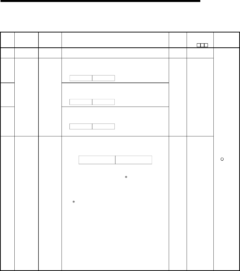
11 - 65 11 - 65
MELSEC-Q
11 TROUBLESHOOTING
Special Register List
(1) Diagnostic Information
Number Name Meaning Explanation
Set by
(When
set)
Corresponding
ACPU
D9
Corresponding
CPU
SD0 Diagnostic
errors
Diagnosis
error code
• Error codes for errors found by diagnosis are stored as BIN data.
• Contents identical to latest fault history information. S (Error) D9008 format
change
SD1
• Year (last two digits) and month that SD0 data was updated is stored
as BCD 2-digit code.
Year (0 to 99) Month (1 to 12)
B15 B7 B0B8to to (Example)
: October, 1995
H9510
SD2
• The day and hour that SD0 was updated is stored as BCD 2-digit
code.
Day (1 to 31) Hour (0 to 23)
B15 B7 B0B8
to to (Example)
: 10 a.m. on 25th
H2510
SD3
Clock time for
diagnosis error
occurrence
Clock time for
diagnosis
error
occurrence
• The minute and second that SD0 data was updated is stored as BCD
2-digit code.
Minutes (0 to 59)
B15 B7 B0B8to to (Example)
: 35 min. 48 sec.
(past the hour)
H3548
Seconds (0 to 59)
S (Error) New
SD4
Error
information
categories
Error
information
category code
Category codes which help indicate what type of information is being
stored in the common information areas (SD5 through SD15) and the
individual information areas (SD16 through SD26) are stored here.
Individual information
category codes Common information
category codes
B15 B7 B0B8
to to
• The common information category codes store the following codes:
0 : No error
1 : Unit/module No./ PLC No./Base No.
2 : File name/Drive name
3 : Time (value set)
4 : Program error location
5 : Switch cause (for Q4AR only)
: For a multiple PLC system, the module number or PLC
number is stored depending on the error that occurred.
(Refer to the corresponding error code for which number
has been stored.)
PLC No. 1: 1, PLC No. 2: 2, PLC No. 3: 3, PLC No. 4: 4
• The individual information category codes store the following codes:
0 : No error
1 : (Open)
2 : File name/Drive name
3 : Time (value actually measured)
4 : Program error location
5 : Parameter number
6 : Annunciator number
7 : Check instruction malfunction number
S (Error) New
+Rem
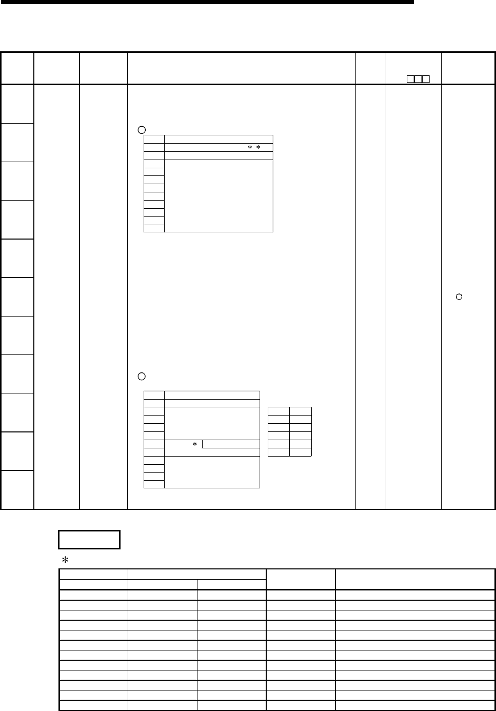
11 - 66 11 - 66
MELSEC-Q
11 TROUBLESHOOTING
Special Register List (Continued)
Number Name Meaning Explanation
Set by
(When
set)
Corresponding
ACPU
D9
Corresponding
CPU
SD5
SD6
SD7
SD8
SD9
SD10
SD11
SD12
SD13
SD14
SD15
Error
common
information
Error
common
information
• Common information corresponding to the error codes (SD0) is stored
here.
• The following five types of information are stored here:
1 Slot No.
SD5
SD6
SD7
SD8
SD9
SD10
SD11
SD12
SD13
SD14
SD15
Meaning
Slot No./PLC No./Base No. 1 2
I/O No.
(Vacant)
Number
*1: For a multiple PLC system, the slot number or PLC number is
stored depending on the error that occurred.
Slot 0 in the multiple PLC system is the one on the slot on the
right of the rightmost CPU module.
(Refer to the corresponding error code for which number has
been stored.)
PLC No. 1: 1, PLC No. 2: 2, PLC No. 3: 3, PLC No. 4: 4
*2: If a fuse blown or I/O verify error occurred in the module loaded
in the MELSECNET/H remote I/O station, the network number is
stored into the upper 8 bits and the station number into the lower
8 bits.
Use the I/O No. to check the module where the fuse blown or I/O
verify error occurred.
2 File name/Drive name
Number
SD5
SD6
SD7
SD8
SD9
SD10
SD11
SD12
SD13
SD14
SD15
Meaning
Drive
2EH(.)
File name
(ASCII code: 8 characters)
(Vacant)
42H(B) 41H(A)
44H(D) 43H(C)
46H(F) 45H(E)
48H(H) 47H(G)
49H(I) 2EH(.)
4BH(K) 4AH(J)
B15 to B8 B7 to B0
(Example)
File name=
ABCDEFGH. IJ
K
Extension
(ASCII code: 3 characters)
3
(Continued to next page)
S (Error) New +Rem
REMARK
3: Extensions are shown below.
SD10 SD11
Higher8 bits Lower8 bits Higher8 bits Extension name File type
51H 50H 41H QPA Parameters
51H 50H 47H QPG Sequence program/SFC program
51H 43H 44H QCD Device comment
51H 44H 49H QDI Device initial value
51H 44H 52H QDR File register
51H 44H 53H QDS Simulation data
51H 44H 4CH QDL Local device
51H 54H 53H QTS Sampling trace data (For QnA)
51H 54H 4CH QTL Status latch data (For QnA)
51H 54H 50H QTP Program trace data (For QnA)
51H 54H 52H QTR SFC trace file
51H 46H 44H QFD Trouble history data
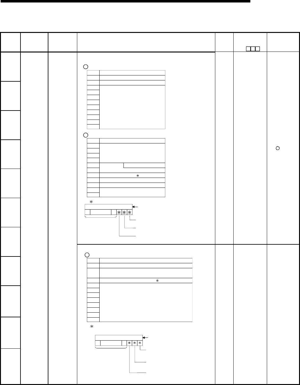
11 - 67 11 - 67
MELSEC-Q
11 TROUBLESHOOTING
Special Register List (Continued)
Number Name Meaning Explanation
Set by
(When
set)
Corresponding
ACPU
D9
Corresponding
CPU
SD5
SD6
SD7
SD8
SD9
SD10
(Continued)
3 Time (value set)
Number
SD5
SD6
SD7
SD8
SD9
SD10
SD11
SD12
SD13
SD14
SD15
Meaning
Time : 1 µs units (0 to 999 µs)
(Vacant)
Time : 1 ms units (0 to 65535 ms)
4 Program error location
Number
SD5
SD6
SD7
SD8
SD9
SD10
SD11
SD12
SD13
SD14
SD15
Meaning
2EH(.)
File name
(ASCII code: 8 characters)
Extension
(ASCII code: 3 characters)
Pattern
Block No.
Step No./transition No.
Sequence step No. (L)
Sequence step No. (H)
4
4 Contents of pattern data
SFC block designation present
(1)/absent (0)
0000 to
0123415 14 to
SFC step designation present
(1)/absent (0)
SFC transition designation
present (1)/absent (0)
(Not used)
(Bit number)
S (Error) New +Rem
SD11
SD12
SD13
SD14
SD15
Error
common
information
Error common
information
5 Switch cause
Switch direction (0:standby system to control
system/ 1: control system to standby system)
Number
SD5
SD6
SD7
SD8
SD9
SD10
SD11
SD12
SD13
SD14
SD15
Meaning
Switch cause (0: automatic switch/ 1: manual switch)
(Vacant)
Tracking flag 5
5 Tracking flag contents
Shows whether or not the tracking data is valid.
Invalid work data
invalid (0) /valid (1)
00
00to
0123415 14 to
System data
(SFC active step information)
invalid (0)/ valid (1)
Switching cause invalid (0)/
valid (1)
(Not used)
(Bit number)
S (Error) New Q4AR
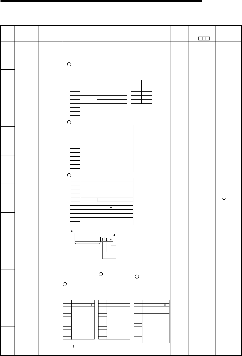
11 - 68 11 - 68
MELSEC-Q
11 TROUBLESHOOTING
Special Register List (Continued)
Number Name Meaning Explanation
Set by
(When
set)
Corresponding
ACPU
D9
Corresponding
CPU
SD16
SD17
SD18
SD19
SD20
SD21
SD22
SD23
• Individual information corresponding to error codes (SD0) is stored
here.
• There are the following six different types of stored information.
1 File name/Drive name
Number
SD16
SD17
SD18
SD19
SD20
SD21
SD22
SD23
SD24
SD25
SD26
Meaning
Drive
2EH(.)
File name
(ASCII code: 8 characters)
(Vacant)
42H(B) 41H(A)
44H(D) 43H(C)
46H(F) 45H(E)
48H(H) 47H(G)
49H(I) 2EH(.)
4BH(K) 4AH(J)
B15 to B8 B7 to B0
(Example)
File name=
ABCDEFGH. IJK
Extension
(ASCII code: 3 characters)
2 Time (value actually measured)
Number
SD16
SD17
SD18
SD19
SD20
SD21
SD22
SD23
SD24
SD25
SD26
Meaning
Time : 1 µs units (0 to 999 µs)
(Vacant)
Time : 1 ms units (0 to 65535 ms)
3 Program error location
Number
SD16
SD17
SD18
SD19
SD20
SD21
SD22
SD23
SD24
SD25
SD26
Meaning
2EH(.)
File name
(ASCII code: 8 characters)
Extension
(ASCII code: 3 characters)
Pattern
Block No.
Step No./transition No.
Sequence step No. (L)
Sequence step No. (H)
Contents of pattern data
SFC block designation present
(1)/absent (0)
0000 to
0123415 14 to
SFC step designation present
(1)/absent (0)
SFC transition designation
present (1)/absent (0)
(Not used)
(Bit number)
SD24 4 Parameter number
5 Annunciator
number / CHK
instruction
malfunction
number
6 Intelligent function
module parameter
error
(for QCPU only)
SD25
SD26
Error individual
information
Error
individual
information
Number
SD16
SD17
SD18
SD19
SD20
SD21
SD22
SD23
SD24
SD25
SD26
Meaning
No.
(Vacant)
Number
SD16
SD17
SD18
SD19
SD20
SD21
SD22
SD23
SD24
SD25
SD26
Meaning
Parameter No.
(Vacant)
Number
SD16
SD17
SD18
SD19
SD20
SD21
SD22
SD23
SD24
SD25
SD26
Meaning
(Vacant)
Parameter No.
Error code for intelligent
function module
6 6
6 For details of the parameter numbers, refer to the user's
manual of the CPU module used.
S (Error) New +Rem
11 - 69 11 - 69
MELSEC-Q
11 TROUBLESHOOTING
Special Register List (Continued)
Number Name Meaning Explanation Set by
(When set)
Corresponding
ACPU
D9
Corresponding
CPU
SD50 Error reset Error code that
performs error reset • Stores error code that performs error reset U New +Rem
SD51 Battery low
latch
Bit pattern
indicating where
battery voltage drop
occurred
• All corresponding bits go ON when battery voltage drops.
• Subsequently, these remain ON even after battery voltage has
been returned to normal.
CPU module battery error
B4 B3 B0B2 B1
Memory card A alarm
Memory card A error
Memory card B alarm
Memory card B error
0< >
-------------------
• When High Performance model QCPU is used, this flag is
always OFF because memory card B is used as standard
memory.
S (Error) New
SD52 Battery low
Bit pattern
indicating where
battery voltage drop
occurred
• Same configuration as SD51 above
• Subsequently, goes OFF when battery voltage is restored to
normal.
• When High Performance model QCPU is used, this flag is
always OFF because memory card B is used as standard
memory.
S (Error) New
SD53
AC/DC
DOWN
detection
Number of times for
AC/DC DOWN
• Every time the input voltage falls to or below 85% (AC
power)/65% (DC power) of the rating during calculation of the
CPU module, the value is incremented by 1 and stored in BIN
code.
S (Error) D9005 +Rem
SD54 MINI link
errors
Error detection
state
1 The relevant station bit goes ON when any of the Installed
MINI (-S3) X(n+0)/X(n+20), X(n+6)/(n+26), X(n+7)/(n+27) or
X(n+8)/X(n+28) goes ON.
2 Goes ON when communications between the installed MINI
(-S3) and the CPU are not possible.
B15 B8B9 B0
8th
module
8th
module
1st
module
1st
module
.........
Information on Information on 1
2
S (Error) D9004 format
change QnA
SD60 Blown fuse
number Number of module
with blown fuse • Value stored here is the lowest station I/O number of the module
with the blown fuse. S (Error) D9000
SD61
I/O module
verification
error number
I/O module
verification error
module number
• The lowest I/O number of the module where the I/O module
verification number took place. S (Error) D9002 +Rem
SD62 Annunciator
number Annunciator
number • The first annunciator number to be detected is stored here. S
(Instruction
execution) D9009
SD63 Number of
annunciators Number of
annunciators • Stores the number of annunciators searched. S
(Instruction
execution) D9124
11 - 70 11 - 70
MELSEC-Q
11 TROUBLESHOOTING
Special Register List (Continued)
Number Name Meaning Explanation Set by
(When set)
Corresponding
ACPU
D9
Corresponding
CPU
SD64 D9125
SD65 D9126
SD66 D9127
SD67 D9128
SD68 D9129
SD69 D9130
SD70 D9131
SD71 D9132
SD72 New
SD73 New
SD74 New
SD75 New
SD76 New
SD77 New
SD78 New
SD79
Table of
detected
annunciator
numbers
Annunciator
detection
number
When F goes ON due to OUT F or SET F , the F numbers which
go progressively ON from SD64 through SD79 are registered.
F numbers turned OFF by RST F are deleted from SD64 to SD79,
and are shifted to the data register following the data register where
the deleted F numbers had been stored.
Execution of the LEDR instruction shifts the contents of SD64 to
SD79 up by one.
(This can also be done by using the INDICATOR RESET switch on
the of the Q3A/Q4ACPU.)
After 16 annunciators have been detected, detection of the 17th will
not be stored from SD64 through SD79.
SD62 0 50 50 50 50 50 50 50 50 50 50 50 99 ...(Number
detected)
SD630123234567898
0 505050505050505050505099SD64
SD65
SD66
SD67
SD68
SD69
SD70
SD71
SD72
SD73
SD74
SD75
SD76
SD77
SD78
SD79
0 0 25 25 99 99 99 99 99 99 99 99 15
0 0 0 99 0 15 15 15 15 15 15 15 70
0 0 0 0 0 0 70 70 70 70 70 70 65
0 0 0 0 0 0 0 656565656538
0 0 0 0 0 0 0 0 38 38 38 38 110
000000000110110110151
00151
0
00000000 151
210
000000000 0 0210
0000000000 0 00
0000000000 0 00
0000000000 0 00
0000000000 0 00
0000000000 0 00
0000000000 0 00
0000000000 0 00
...(Number of
annunciators
detected)
(Number
detected)
SET
F50
SET
F25
SET
F99
RST
F25
SET
F15
SET
F70
SET
F65
SET
F38
SET
F110
SET
F151
SET
F210LEDR
S
(Instruction
execution)
New
SD80 CHK number CHK number • Error codes detected by the CHK instruction are stored as BCD
code.
S
(Instruction
execution)
New
SD90 Corresponds to SM90 D9108
SD91 Corresponds to SM91 D9109
SD92 Corresponds to SM92 D9110
SD93 Corresponds to SM93 D9111
SD94 Corresponds to SM94 D9112
SD95 Corresponds to SM95 D9113
SD96 Corresponds to SM96 D9114
SD97 Corresponds to SM97 New
SD98 Corresponds to SM98 New
SD99
Step transition
watchdog
timer setting
value
(Enabled only
when SFC
program
exists)
F number for
timer set value
and time over
error
Corresponds to SM99
• F numbers which go ON at step transition
watchdog timer set value and watchdog timer
over errors.
B15 B7 B0B8
F number setting
(0 to 255)
Timer time limit
setting
(1 to 255 s:
(1-s units))
• Timer is started by turning SM90 through
SM99 ON during active step, and if the
transition conditions for the relevant steps are
not met within the timer limits, the designated
annunciator (F) will go ON.
U
New
SD105
CH1
transmission
speed setting
(RS-232)
Stores the
preset
transmission
speed when
GX Developer
is used.
3 : 300bps, 6 : 600bps, 24 : 2400bps, 48 : 4800bps
96 : 9600bps, 192 : 19.2kbps, 384 : 38.4kbps
576 : 57.6kbps, 1152 : 115.2kbps
S New QCPU
Remote
11 - 71 11 - 71
MELSEC-Q
11 TROUBLESHOOTING
Special Register List
(2) System information
Number Name Meaning Explanation Set by
(When set)
Corresponding
ACPU
D9
Corresponding
CPU
• The switch status of the remote I/O module is stored in the following
format.
B15 B4 B3 B0
1
Vacant
1 Remote I/O module switch status Always 1: STOP
S (Always) New Remote
• The CPU module switch status is stored in the following format:
B15 B12B11 B8 B7 B4 B3 B0
Vacant
3 2 1
1: CPU switch status 0: RUN
1: STOP
2: L.CLR
2: Memory card switch Always OFF
3: DIP switch B8 through BC correspond to SW1
through SW5 of system setting
switch 1.
0: OFF, 1: ON
BD through BF are vacant.
S(Every
END
processing)
New QCPU
• The CPU module switch status is stored in the following format:
B15 B12B11 B8 B7 B4 B3 B0
Vacant
3 2 1
1: CPU key
Status of switch
0 : RUN
1 : STOP
2 : L.CLR
2: Memory cards switch B4 corresponds to card A, and B5
corresponds to card B
OFF at 0; ON at 1
3: DIP switch B8 through B12 correspond to
SW1 through SW5 of system
setting switch 1.
B14 and B15 correspond to SW1
and SW2 of system setting switch
2, respectively.
OFF at 0; ON at 1
SD200 Status of
switch
Status of CPU
switch
S(Every
END
processing)
New QnA
11 - 72 11 - 72
MELSEC-Q
11 TROUBLESHOOTING
Special Register List (Continued)
Number Name Meaning Explanation Set by
(When set)
Corresponding
ACPU
D9
Corresponding
CPU
• The following bit patterns are used to store the statuses of the LEDs
on the CPU module:
• 0 indicates OFF, 1 ON, and 2 flicker.
B15 B12B11 B8B7 B4B3 B0
83 2 1
456
7
1: RUN
2: ERROR
3: USER
4: BAT.ALARM
5: BOOT
6: Vacant
7: Vacant
8: MODE
Bit patterns for MODE
0: OFF, 1: Green,
2: Orange
S (Status
change) New QCPU
• Information concerning which of the following status the LEDs on the
CPU module are in is stored in the following bit patterns:
• 0 is off, 1 is on, and 2 is flicker
B15 B12B11 B8 B7 B4 B3 B0
83 2 1
456
7
1: RUN
2: ERROR
3: USER
4: BAT.ALARM
5: BOOT
6: CARD A (Memory card)
7: CARD B (Memory card)
8: Vacant
SD201 LED status Status of
CPU-LED
S (Status
change) New QnA
SD202 LED off
Bit pattern of
LED that is
turned off
• Stores bit patterns of LEDs turned off
(Only USER and BOOT enabled)
• Turned off at 1, not turned off at 0
U New QnA
• The operating status of the remote I/O module is stored in the
following format.
B15 B4 B3 B0
1
Vacant
1 Remote I/O module operating status Always 2: STOP
S (Always) New Remote
• The CPU module operating status is stored as indicated in the
following figure:
B15 B12B11 B8 B7 B4 B3 B0
21
1: Operating status of CPU 0 :RUN
1 :STEP-RUN
2 :STOP
3 :PAUSE
2: STOP/PAUSE cause 0 :Switch
1 :Remote contact
2 : Remote operation from the
GX Developer or Serial
Communication.
3 :Internal program instruction
Note: Priority is earliest first 4 :Errors
SD203
Operating
status of
CPU
Operating
status of CPU
S (Every
END
processing)
D9015 format
change
SD206
Device test
execution
type
0: Test not yet
executed
1: During X
device test
2: During Y
device test
3: During X/Y
device test
• Set when the device test mode is executed on GX Developer. S
(Request) New Remote
11 - 73 11 - 73
MELSEC-Q
11 TROUBLESHOOTING
Special Register List (Continued)
Number Name Meaning Explanation Set by
(When set)
Corresponding
ACPU
D9
Corresponding
CPU
SD207 Priorities 1 to 4 D9038
SD208 Priorities 5 to 8 D3039 format
change
SD209
LED display
priority
ranking Priorities 9 to
10
• When error is generated, the LED display (flicker) is made according
to the error number setting priorities.
• The setting areas for priorities are as follows:
B15 B12B11 B8 B7 B4 B3 B0
Priority 4 Priority 3 Priority 2 Priority 1
SD207 Priority 8 Priority 7 Priority 6 Priority 5
SD208 Priority 10 Priority 9
SD209
Default Value SD207=H4321
SD208=H8765
SD207=H00A9
• No display is made if "0" is set.
However, even if "0" has been set, information concerning CPU
module operation stop (including parameter settings) errors will be
indicated by the LEDs without conditions.
U
New
SD210 Clock data Clock data
(year, month)
• The year (last two digits) and month are stored as BCD code at
SD210 as shown below:
B15 B12B11 B8 B7 B4 B3 B0
Year Month
Example :
July 1993
H9307
to to to to
D9025
SD211 Clock data Clock data
(day, hour)
• The day and hour are stored as BCD code at SD211 as shown
below:
B15 B12B11 B8 B7 B4 B3 B0
Da
y
Hour
Example :
31st, 10 a.m.
H3110
to to to to
D9026
SD212 Clock data
Clock data
(minute,
second)
• The minutes and seconds (after the hour) are stored as BCD code at
SD212 as shown below: Example :
B15 B12B11 B8 B7 B4 B3 B0
to to to to
Minute Second
35 min., 48 sec.
(after the hour)
H3548
S/U
(Request)
D9027
+Rem
Clock data
(higher digits of
year, day of
week)
• Stores the year (two digits) and the day of the week in SD213 in the
BCD code format as shown below.
B15 B12B11 B8 B7 B4 B3 B0
to to to to
Higher digits
of year (0 to 99)
Day of week
0
1
2
3
4
5
6
Sunday
Monday
Tuesday
Wednesday
Thursday
Friday
Saturday
Example :
Friday
H0005
S/U
(Request) D9028 QCPU
Remote
SD213 Clock data
Clock data
(day of week)
• The day of the week is stored as BCD code at SD213 as shown
below:
B15 B12B11 B8 B7 B4 B3 B0
Always set "0"
Day of week
0
1
2
3
4
5
6
Sunday
Monday
Tuesday
Wednesday
Thursday
Friday
Saturday
Example :
Friday
H0005
to to to to
S/U
(Request) D9028 QnA
11 - 74 11 - 74
MELSEC-Q
11 TROUBLESHOOTING
Special Register List (Continued)
Number Name Meaning Explanation Set by
(When set)
Corresponding
ACPU
D9
Corresponding
CPU
SD220
SD221
SD222
SD223
SD224
SD225
SD226
SD227
LED display
data
Display indicator
data
• LED display ASCII data (16 characters) stored here.
SD220
SD221
SD222
SD223
SD224
SD225
SD226
SD227
15th character from the right
13th character from the right
11th character from the right
9th character from the right
7th character from the right
5th character from the right
3rd character from the right
1st character from the right
16th character from the right
14th character from the right
12th character from the right
10th character from the right
8th character from the right
6th character from the right
4th character from the right
2nd character from the right
toB15 B8 toB7 B0
S (When
changed) New
SD240 Base mode 0: Automatic mode
1: Detail mode • Stores the base mode. S (Initial) New
SD241
No. of
extension
bases
0: Main base only
1 to 7: No. of
extension
bases
• Stores the maximum number of the extension bases unit being
installed. S (Initial) New
SD242 A/Q base
differentiation
Base type
differentiation
0: QA B is
installed
(A mode)
1: Q B is
installed
(Q mode)
B0
Fixed to 0
Main base unit
B1B2
B7
1st expansion
base
to
2nd expansion
base
7th expansion
base
to
When no expansion
base is installed, the
value is fixed to 0.
S (Initial) New
SD243
SD244
No. of base
slots No. of base slots
SD243 Expansion 3 Expansion 2 Expansion 1 Main
Expansion 7 Expansion 6 Expansion 5 Expansion 4
SD244
B15 B12 B11 B8 B7 B4 B3 B0
• As shown above, each area stores the number of slots being
installed.
S (Initial) New
QCPU
Remote
SD250 Loaded
maximum I/O
Loaded maximum
I/O No.
• When SM250 goes from OFF to ON, the upper 2 digits of the final
I/O number plus 1 of the modules loaded are stored as BIN values.
S
(Request
END)
New +Rem
SD251
Head I/O
number for
replacement
Head I/O No. for
module
replacement
• Stores the upper two digits of the first I/O number of an I/O module
that is removed/replaced in the online status.(default value : 100H) U D9094
Q2A (S1)
Q3A
Q4A
Q4AR
SD253 RS-422 baud
rate RS-422 baud rate • Stores baud rate of RS-422.
0: 9600bps 1: 19.2kbps 2: 38.4kbps
S (When
changed) New QnA
SD254 Number of
modules installed • Indicates the number of modules installed on MELSECNET/10 (H).
SD255 I/O No. • MELSECNET/10 (H) I/O number of first module installed
SD256 Network
No. • MELSECNET/10 (H) network number of first module installed
SD257 Group
number • MELSECNET/10 (H) group number of first module installed
SD258 Station
No. • MELSECNET/10 (H) station number of first module installed
SD259
Informa-
tion from
1st
module
Standby
informa-
tion
• In the case of standby stations, the module number of the standby
station is stored. (1 to 4)
SD260
to
SD264
Information from
2nd module • Configuration is identical to that for the first module.
SD265
to
SD269
Information from
3rd module • Configuration is identical to that for the first module.
SD270
to
SD274
MELSECNET
/10 (H)
information
Information from
4th module • Configuration is identical to that for the first module.
S (Initial) New
11 - 75 11 - 75
MELSEC-Q
11 TROUBLESHOOTING
Special Register List (Continued)
Number Name Meaning Explanation Set by
(When set)
Corresponding
ACPU
D9
Corresponding
CPU
1 When Xn0 of the installed CC-Link goes ON, the bit
corresponding to the station switches ON.
2 When either Xn1 or XnF of the installed CC-Link switch OFF, the
bit corresponding to the station switches ON.
3 Switches ON when the CPU module cannot communicate with
the installed CC-Link.
B0
1st module
2nd module
3rd module
B3B4B7B8
B11B12
B15
Vacant
4th module
Information
of 1
Information
of 2
Information
of 3
The above module numbers n are in order of the head I/O Nos.
(However, the modules without parameter setting are not counted in.)
S (Error) New QCPU
Remote
SD280 CC-Link error
Error detection
status
1 When Xn0 of the installed CC-Link goes ON, the bit
corresponding to the station switches ON.
2 When either Xn1 or XnF of the installed CC-Link switch OFF, the
bit corresponding to the station switches ON.
3 Switches ON when the CPU module cannot communicate with
the installed CC-Link.
B15 B8B9 B0
8th
module
8th
module
1st
module
1st
module
...
toto
...
Information of 1
Information of 2
S (Error) New QnA
SD290 Number of
points
allocated for X • Stores the number of points currently set for X devices
SD291 Number of
points
allocated for Y • Stores the number of points currently set for Y devices
SD292 Number of
points
allocated for M • Stores the number of points currently set for M devices
+Rem
SD293 Number of
points
allocated for L • Stores the number of points currently set for L devices
SD294 Number of
points
allocated for B • Stores the number of points currently set for B devices +Rem
SD295 Number of
points
allocated for F • Stores the number of points currently set for F devices
SD296
Number of
points
allocated for
SB
• Stores the number of points currently set for SB devices +Rem
SD297 Number of
points
allocated for V • Stores the number of points currently set for V devices
SD298 Number of
points
allocated for S • Stores the number of points currently set for S devices
SD299 Number of
points
allocated for T • Stores the number of points currently set for T device
SD300
Number of
points
allocated for
ST
• Stores the number of points currently set for ST devices
SD301
Device
allocation
(Same as
parameter
contents)
Number of
points
allocated for C • Stores the number of points currently set for C devices
S (Initial) New
11 - 76 11 - 76
MELSEC-Q
11 TROUBLESHOOTING
Special Register List (Continued)
Number Name Meaning Explanation Set by
(When set)
Corresponding
ACPU
D9
Corresponding
CPU
SD302 Number of points
allocated for D • Stores the number of points currently set for D devices
SD303 Number of points
allocated for W • Stores the number of points currently set for W devices
SD304
Device
allocation
(Same as
parameter
contents) Number of points
allocated for SW • Stores the number of points currently set for SW devices
S (Initial) New +Rem
SD315
Time
reserved for
communicat
ion
processing
Time reserved for
communication
processing
Reserves the designated time for communication processing with
GX Developer or other units.
The greater the value is designated, the shorter the response time
for communication with other devices (GX Developer, serial
communication units) becomes.
Setting range: 1 to 100 ms
If the designated value is out of the range above, it is assumed to
no setting.
U
(END
processing)
New QCPU
SD340 No. of modules
installed • Indicates the number of modules installed on Ethernet.
SD341 I/O No. • Ethernet I/O No. of the 1st module installed.
SD342 Network
No. • Ethernet network No. of the 1st module installed.
SD343 Group No. • Ethernet group No. of the 1st module installed.
SD344 Station
No. • Ethernet station No. of the 1st module installed.
SD345 to
SD346 Vacant
• Vacant
(With High Performance model QCPU, the Ethernet IP address
of the 1st module is stored in buffer memory.)
SD347
Informa-
tion of 1st
module
Vacant
• Vacant
(With High Performance model QCPU, the Ethernet error code of
the 1st module is read with the ERRORRD instruction.)
S (Initial) New
SD348 to
SD354
Information from 2nd
module • Configuration is identical to that for the first module.
SD355 to
SD361
Information from 3rd
module • Configuration is identical to that for the first module.
SD362 to
SD368
Ethernet
information
Information from
4th module • Configuration is identical to that for the first module.
S (Initial) New
QCPU
Remote
SD340 No. of modules
installed • Indicates the number of modules installed on Ethernet.
SD341 I/O No. • Ethernet I/O No. of the 1st module installed.
SD342 Network
No. • Ethernet network No. of the 1st module installed.
SD343 Group No. • Ethernet group No. of the 1st module installed.
SD344 Station
No. • Ethernet station No. of the 1st module installed.
SD345 to
SD346 IP address • Ethernet IP address of the 1st module installed.
SD347
Informa-
tion of 1st
module
Error code • Ethernet error code of the 1st module installed.
SD348 to
SD354
Information from 2nd
module • Configuration is identical to that for the first module.
SD355 to
SD361
Information from 3rd
module • Configuration is identical to that for the first module.
S (Initial) New
SD362 to
SD368
Ethernet
information
Information from 4th
module • Configuration is identical to that for the first module. S (Initial) New
SD380
Ethernet
instruction
reception
status
Instruction reception
status of 1st module
B0
Instruction reception status of channel 1
Instruction reception status of channel 2
B1B2B3B4B5B6B7B8B15
Instruction reception status of channel 3
Instruction reception status of channel 4
Instruction reception status of channel 5
Instruction reception status of channel 6
Instruction reception status of channel 7
Instruction reception status of channel 8
ON: Received (Channel is used.)
OFF: Not received (Channel is not used.)
00to
Not used
S (Initial) New
QnA
11 - 77 11 - 77
MELSEC-Q
11 TROUBLESHOOTING
Special Register List (Continued)
Number Name Meaning Explanation Set by
(When set)
Corresponding
ACPU
D9
Corresponding
CPU
SD381 Information from
2nd module • Configuration is identical to that for the first module.
SD382 Information from
3rd module • Configuration is identical to that for the first module.
SD383
Ethernet
instruction
reception
status Information from
4th module • Configuration is identical to that for the first module.
S (Initial) New
SD392 Software
version
Internal system
software version
• Stores the internal system software version in ASCII code.
Higher byte Lower byte
The software version is stored
in the lower byte position.
The data in the higher byte
position is indefinite.
For version "A", for example, "41H" is stored.
Note: The internal system software version may differ from the
version indicated by the version symbol printed on the
case.
S (Initial) D9060
QnA
SD395 Multiple PLC
number
Multiple PLC
number
• In a multiple PLC system configuration, the PLC number of the
host CPU is stored.
PLC No. 1: 1, PLC No. 2: 2, PLC No. 3: 3, PLC No. 4: 4
S (Initial) New QCPU function
Ver. B or later
(3) System clocks/counters
Number Name Meaning Explanation Set by
(When set)
Corresponding
ACPU
D9
Corresponding
CPU
SD412 1 second
counter
Number of counts in
1-second units
• Following programmable controller CPU module RUN, 1 is
added each second
• Count repeats from 0 to 32767 to -32768 to 0
S (Status
change) D9022
SD414
2n second
clock
setting
2n second clock
units
• Stores value n of 2n second clock (Default is 30)
• Setting can be made between 1 and 32767 U New
SD415 2nms clock
setting 2nms clock units • Stores value n of 2nms clock (Default is 30)
• Setting can be made between 1 and 32767 U New QCPU
SD420 Scan
counter
Number of counts in
each scan
• Incremented by 1 for each scan execution after the CPU module
is set to RUN.
• Count repeats from 0 to 32767 to -32768 to 0
S(Every
END
processing)
New
SD430
Low speed
scan
counter
Number of counts in
each scan
• Incremented by 1 for each scan execution after the CPU module
is set to RUN.
• Count repeats from 0 to 32767 to -32768 to 0
• Used only for low speed execution type programs
S(Every
END
processing)
New
: Not counted by the scan in an initial execution type program.
11 - 78 11 - 78
MELSEC-Q
11 TROUBLESHOOTING
Special Register List
(4) Scan information
Number Name Meaning Explanation Set by
(When set)
Corresponding
ACPU
D9
Corresponding
CPU
SD500 Execution
program No.
Execution type of
program being
executed
• Program number of program currently being executed is
stored as BIN value.
S (Status
change) New
SD510 Low speed
program No.
File name of low
speed execution in
progress
• Program number of low speed program currently being
executed is stored as BIN value.
• Enabled only when SM510 is ON.
S (Every
END
processing)
New
SD520 Current scan time
(ms unit)
S (Every
END
processing)
D9017 format
change
SD521
Current scan
time Current scan time
(µs unit)
• Current scan time is stored into SD520, SD521.
(Measurement is made in 100µs increments.)
SD520: Place of ms is stored (storage range: 0 to 65535)
SD521: Place of µs is stored (storage range: 0 to 900)
Example: Current scan time 23.6ms is stored as indicated
below.
SD520 = 23
SD521 = 600
S (Every
END
processing)
New
SD522 Initial scan time
(ms unit)
SD523
Initial scan
time Initial scan time
(µs unit)
• Scan time of initial execution program is stored into SD522,
SD523. (Measurement is made in 100µs increments.)
SD522: Place of ms is stored (storage range: 0 to 65535)
SD523: Place of µs is stored (storage range: 0 to 900)
S (First
END
processing)
New
SD524 Minimum scan time
(ms unit)
S (Every
END
processing)
D9018 format
change
SD525
Minimum scan
time Minimum scan time
(µs unit)
• Minimum value of scan time with the exception of initial
execution program scan time is stored into SD524, SD525.
(Measurement is made in 100µs increments.)
SD524: Place of ms is stored (storage range: 0 to 65535)
SD525: Place of µs is stored (storage range: 0 to 900)
S (Every
END
processing)
New
SD526 Maximum scan time
(ms unit)
D9019 format
change
SD527
Maximum scan
time Maximum scan time
(µs unit)
• Maximum value of scan time with the exception of initial
execution program scan time is stored into SD526, SD527.
(Measurement is made in 100µs increments.)
SD526: Place of ms is stored (storage range: 0 to 65535)
SD527: Place of µs is stored (storage range: 0 to 900)
S (Every
END
processing) New
SD528 Current scan time
(ms unit)
SD529
Current scan
time
for low speed
execution type
programs
Current scan time
(µs unit)
• Current scan time of low speed program is stored into
SD528, SD529. (Measurement is made in 100µs
increments.)
SD528: Place of ms is stored (storage range: 0 to 65535)
SD529: Place of µs is stored (storage range: 0 to 900)
S (Every
END
processing)
New
SD532 Minimum scan time
(ms unit)
SD533
Minimum scan
time for
low speed
execution type
programs
Minimum scan time
(µs unit)
• Minimum value of low speed program scan time is stored
into SD532, SD533. (Measurement is made in 100µs
increments.)
SD532: Place of ms is stored (storage range: 0 to 65535)
SD533: Place of µs is stored (storage range: 0 to 900)
S (Every
END
processing)
New
SD534 Maximum scan time
(ms unit)
SD535
Maximum scan
time for
low speed
execution type
programs
Maximum scan time
(µs unit)
• Maximum value of low speed program scan time with the
exception of the first scan is stored into SD534, SD535.
(Measurement is made in 100µs increments.)
SD534: Place of ms is stored (storage range: 0 to 65535)
SD535: Place of µs is stored (storage range: 0 to 900)
S (Every
END
processing)
New
SD540 END processing time
(ms unit)
SD541
END
processing
time END processing time
(µs unit)
• Time from scan program end until next scan start is stored
into SD540, SD541. (Measurement is made in 100µs
increments.)
SD540: Place of ms is stored (storage range: 0 to 65535)
SD541: Place of µs is stored (storage range: 0 to 900)
S (Every
END
processing)
New
11 - 79 11 - 79
MELSEC-Q
11 TROUBLESHOOTING
Special Register List (Continued)
Number Name Meaning Explanation Set by
(When set)
Corresponding
ACPU
D9
Corresponding
CPU
SD542 Constant scan
waiting time (ms unit)
SD543
Constant scan
wait time Constant scan
waiting time (µs unit)
• Waiting time at the time of constant scan setting is stored
into SD542, SD543. (Measurement is made in 100µs
increments.)
SD542: Place of ms is stored (storage range: 0 to 65535)
SD543: Place of µs is stored (storage range: 0 to 900)
S (First
END
processing)
New
SD544
Low speed program
cumulative execution
time (ms unit)
SD545
Cumulative
execution time
for low speed
execution type
programs
Low speed program
cumulative execution
time (µs unit)
• Cumulative execution time of low speed program is stored
into SD544, SD545. (Measurement is made in 100µs
increments.)
SD544: Place of ms is stored (storage range: 0 to 65535)
SD545: Place of µs is stored (storage range: 0 to 900)
• Cleared to 0 after end of low speed one scan.
S (Every
END
processing)
New
SD546
Low speed program
execution time
(ms unit)
SD547
Execution time
for low speed
execution type
programs
Low speed program
execution time
(µs unit)
• Execution time of low speed program during one scan is
stored into SD546, SD547. (Measurement is made in 100µs
increments.)
SD546: Place of ms is stored (storage range: 0 to 65535)
SD547: Place of µs is stored (storage range: 0 to 900)
• Stored every scan.
S (Every
END
processing)
New
SD548
Scan program
execution time
(ms unit)
SD549
Scan program
execution time Scan program
execution time
(µs unit)
• Execution time of scan program during one scan is stored
into SD548, SD549. (Measurement is made in 100µs
increments.)
SD548: Place of ms is stored (storage range: 0 to 65535)
SD549: Place of µs is stored (storage range: 0 to 900)
• Stored every scan.
S (Every
END
processing)
New
SD550
Service
interval
measurement
module
Unit/module No. • Sets I/O number for module that measures service interval U New
SD551 Module service
intervals (ms unit)
SD552
Service
interval time Module service
intervals (µs unit)
• Service intervals for the module specified in SD550 are
stored into SD551, SD552 when SM551 is turned ON.
(Measurement is made in 100µs increments.)
SD551: Place of ms is stored (storage range: 0 to 65535)
SD552: Place of µs is stored (storage range: 0 to 900)
S
(Request) New
+Rem
11 - 80 11 - 80
MELSEC-Q
11 TROUBLESHOOTING
Special Register List
(5) Memory card
Number Name Meaning Explanation Set by
(When set)
Corresponding
ACPU
D9
Corresponding
CPU
• Indicates memory card A model installed
Drive 1
(RAM) model
Drive 2
(ROM) model
0: Does not exist
1: SRAM
0: Does not exist
(1: SRAM)
2: ATA FRASH
3: Flash ROM
B4 B3 B0B8 B7B15
0< >0
-----------
S (Initial and card
removal) New QCPU
SD600
Memory
card A
models
Memory
card A
models • Indicates memory card A model installed
B4 B3 B0
Drive 1
(RAM) model
Drive 2
(ROM) model
0< >0
0: Does not exist
1: SRAM
0: Does not exist
2: E PROM
3: Flash ROM
B8 B7B15
-----------
2
S (Initial and card
removal) New QnA
S (Initial and card
removal) New QCPU
SD602
Drive 1
(RAM)
capacity
Drive 1
capacity • Drive 1 capacity is stored in 1 kbyte units S (Initial and card
removal) New QnA
S (Initial and card
removal) New QCPU
SD603
Drive 2
(ROM)
capacity
Drive 2
capacity • Drive 2 capacity is stored in 1 kbyte units S (Initial and card
removal) New QnA
• The use conditions for memory card A are stored as bit patterns
(In use when ON)
• The significance of these bit patterns is indicated below:
B0: Boot operation (QBT)
B1: Parameters (QPA)
B2: Device comments (QCD)
B3: Device initial value (QDI)
B4: File register R (QDR)
B5: Trace (QTS)
B6: Not used
B7: Not used
B8: Not used
B9: CPU fault history (QFD)
BA: SFC trace (QTS)
BB: Local device (QDL)
BC: Not used
BD: Not used
BE: Not used
BF: Not used
S (Status change) New QCPU
• The use conditions for memory card A are stored as bit patterns
(In use when ON)
• The significance of these bit patterns is indicated below:
B0: Boot operation (QBT)
B1: Parameters (QPA)
B2: Device comments (QCD)
B3: Device initial value (QDI)
B4: File register R (QDR)
B5: Sampling trace (QTS)
B6: Status latch (QTL)
B7: Program trace (QTP)
B8: Simulation data (QDS)
B9: CPU fault history (QFD)
B10: SFC trace (QTS)
B11: Local device (QDL)
B12: Not used
B13: Not used
B14: Not used
B15: Not used
SD604
Memory
card A use
conditions
Memory
card A
use
conditions
S (Status change) New QnA
SD620
Memory
card B
models
Memory
card B
models
• Indicates memory card B models installed
Drive 3
(RAM) model
Drive 4
(ROM) model
(0: Does not exist)
1: SRAM
0: Does not exist
(1: SRAM)
(2: E PROM)
3: Flash ROM
B4 B3 B0B8 B7B15
0< >0
-----------
2
Drive 4 is fixed to "3" because it has built-in Flash ROM.
S (Initial) New QCPU
11 - 81 11 - 81
MELSEC-Q
11 TROUBLESHOOTING
Special Register List (Continued)
Number Name Meaning Explanation
Set by
(When
set)
Corresponding
ACPU
D9
Corresponding
CPU
SD620 Memory card
B models
Memory card
B models
• Indicates memory card B models installed
B4 B3 B0
Drive 1
(RAM) model
Drive 2
(ROM) model
0< >0
0: Does not exist
1: SRAM
0: Does not exist
2: E
2
PROM
3: Flash ROM
B8 B7B15
-----------
S (Initial) New
Q2A (S1)
Q3A
Q4A
Q4AR
• Drive 3 capacity is stored in 1 kbyte units. S (Initial) New QCPU
SD622
Drive 3
(RAM)
capacity
Drive 3
capacity • Drive 3 capacity is stored in 1 kbyte units S (Initial) New
Q2A (S1)
Q3A
Q4A
Q4AR
• Drive 4 capacity is stored in 1 kbyte units. S (Initial) New QCPU
SD623
Drive 4
(ROM)
capacity
Drive 4
capacity • Drive 4 capacity is stored in 1 kbyte units S (Initial) New
Q2A (S1)
Q3A
Q4A
Q4AR
• The conditions for usage for drive 3/4 are stored as bit patterns.
(In use when ON)
• The significance of these bit patterns is indicated below:
B0: Boot operation (QBT)
B1: Parameters (QPA)
B2: Device comments (QCD)
B3: Device initial value (QDI)
B4: File R (QDR)
B5: Trace (QTS)
B6: Not used
B7: Not used
B8: Not used
B9: CPU fault history (QFD)
B10: SFC trace (QTS)
B11: Local device (QDL)
B12: Not used
B13: Not used
B14: Not used
B15: Not used
Drive 3/4 use
conditions
Drive 3/4 use
conditions
S (Status
change) New QCPU
• The use conditions for memory card B are stored as bit patterns
(In use when ON)
• The significance of these bit patterns is indicated below:
B0: Boot operation (QBT)
B1: Parameters (QPA)
B2: Device comments (QCD)
B3: Device initial value (QDI)
B4: File R (QDR)
B5: Sampling trace (QTS)
B6: Status latch (QTL)
B7: Program trace (QTP)
B8: Simulation data (QDS)
B9: CPU fault history (QFD)
B10: SFC trace (QTS)
B11: Local device (QDL)
B12: Not used
B13: Not used
B14: Not used
B15: Not used
SD624
Memory card
B use
conditions
Memory card
B use
conditions
S (Status
change) New
Q2A (S1)
Q3A
Q4A
Q4AR
SD640 File register
drive Drive number: • Stores drive number being used by file register S (Initial) New
SD641
SD642
SD643
SD644
SD645
SD646
File register
file name
File register
file name
• Stores file register file name (with extension) selected at parameters
or by use of QDRSET instruction as ASCII code.
SD641
SD642
SD643
SD644
SD645
SD646
Second character
Fourth character
Sixth character
Eighth character
First character of extension
Third character of extension
First character
Third character
Fifth character
Seventh character
2EH(.)
Second character of
extension
B15 to B8 B7 to B0
S (Initial) New
SD647 File register
capacity
File register
capacity
• Stores the data capacity of the currently selected file register in 1 k
word units.
S (Status
change) New
SD648 File register
block number
File register
block number • Stores the currently selected file register block number. S (Status
change) D9035
SD650 Comment
drive
Comment
drive number
• Stores the comment drive number selected at the parameters or by
the QCDSET instruction.
S (Status
change) New
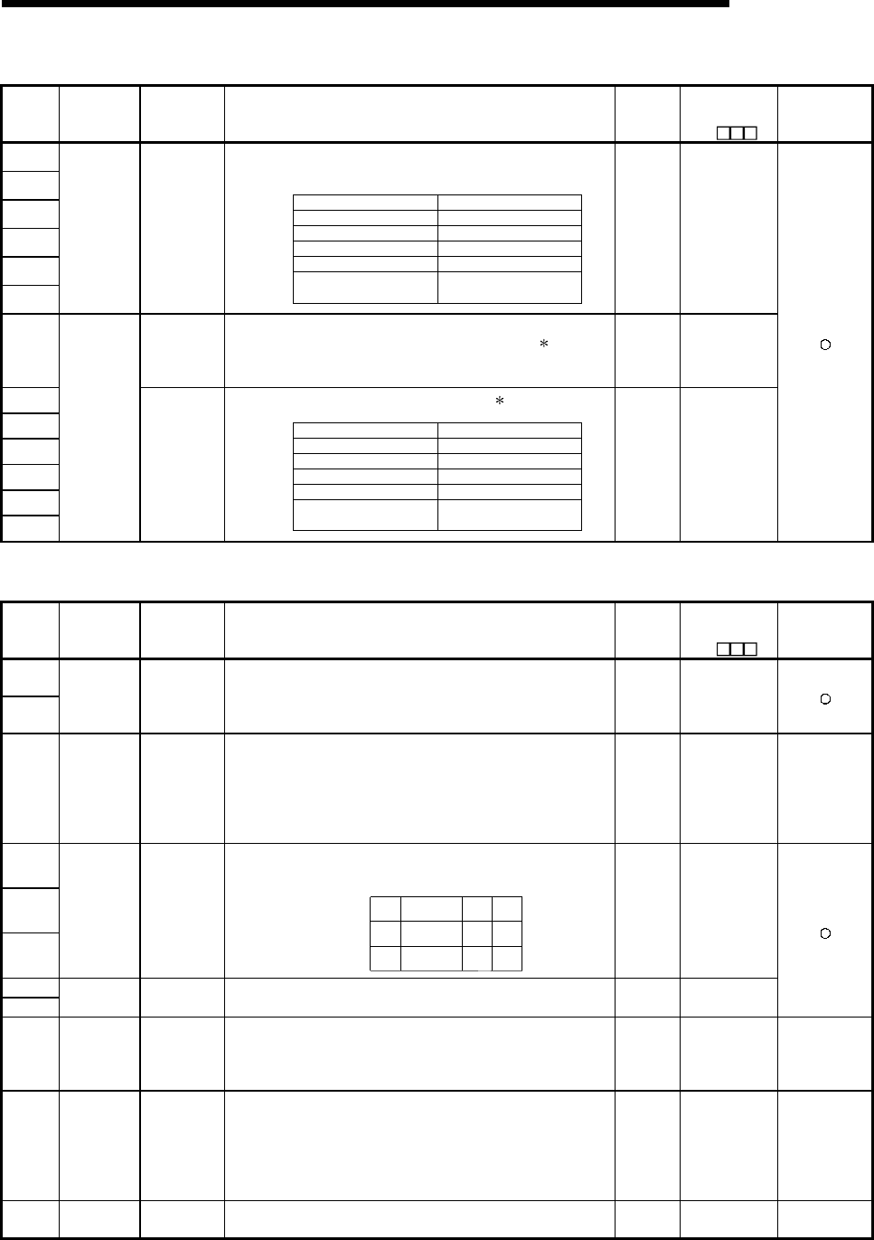
11 - 82 11 - 82
MELSEC-Q
11 TROUBLESHOOTING
Special Register List (Continued)
Number Name Meaning Explanation
Set by
(When
set)
Corresponding
ACPU
D9
Corresponding
CPU
SD651
SD652
SD653
SD654
SD655
SD656
Comment file
name
Comment file
name
• Stores the comment file name (with extension) selected at the
parameters or by the QCDSET instruction in ASCII code.
S
D651
S
D652
S
D653
S
D654
S
D655
S
D656
Second character
Fourth character
Sixth character
Eighth character
First character of extension
Third character of extension
First character
Third character
Fifth character
Seventh character
2EH(.)
Second character of
extension
B15 to B8 B7 to B0
S (Status
change) New
SD660
Boot
designation
file drive
number
• Stores the drive number where the boot designation file ( .QBT) is
being stored. S (Initial) New
SD661
SD662
SD663
SD664
SD665
SD666
Boot
operation
designation
file
File name of
boot
designation
file
• Stores the file name of the boot designation file ( .QBT).
S
D661
S
D662
S
D663
S
D664
S
D665
S
D666
Second character
Fourth character
Sixth character
Eighth character
First character of extension
Third character of extension
First character
Third character
Fifth character
Seventh character
2EH(.)
Second character of
extension
B15 to B8 B7 to B0
S (Initial) New
(6) Instruction-Related Registers
Number Name Meaning Explanation
Set by
(When
set)
Corresponding
ACPU
D9
Corresponding
CPU
SD705
SD706
Mask pattern Mask pattern
• During block operations, turning SM705 ON makes it possible to use
the mask pattern being stored at SD705 (or at SD705 and SD706 if
double words are being used) to operate on all data in the block with
the masked values.
U New
SD714
Number of
vacant
communicati
on request
registration
areas
0 to 32 • Stores the number of vacant blocks in the communications request
area for remote terminal modules connected to the AJ71PT32-S3.
S (During
execution) D9081 QnA
SD715
SD716
SD717
IMASK
instruction
mask pattern
Mask pattern
• Patterns masked by use of the IMASK instruction are stored in the
following manner:
SD715
SD716
SD717
l15 l1 l0
l31
l47
l17
l33
l16
l32
B15 B0B1
to
to
to
S (During
execution) New
SD718
SD719 Accumulator Accumulator • For use as replacement for accumulators used in A-series programs. S/U New
SD720
Program No.
designation
for PLOAD
instruction
Program No.
designation
for PLOAD
instruction
• Stores the program number of the program to be loaded by the
PLOAD instruction when designated.
• Designation range: 1 to 124
U New QCPU
SD730
No. of vacant
registration
area for CC-
Link
communicati
on request
0 to 32
• Stores the number of vacant registration area for the request for
communication with the intelligent device station connected to
A(1S)J61QBT61.
S (During
execution) New QnA
SD736 PKEY input PKEY input • Special register that temporarily stores keyboard data input by means
of the PKEY instruction.
S (During
execution) New QnA
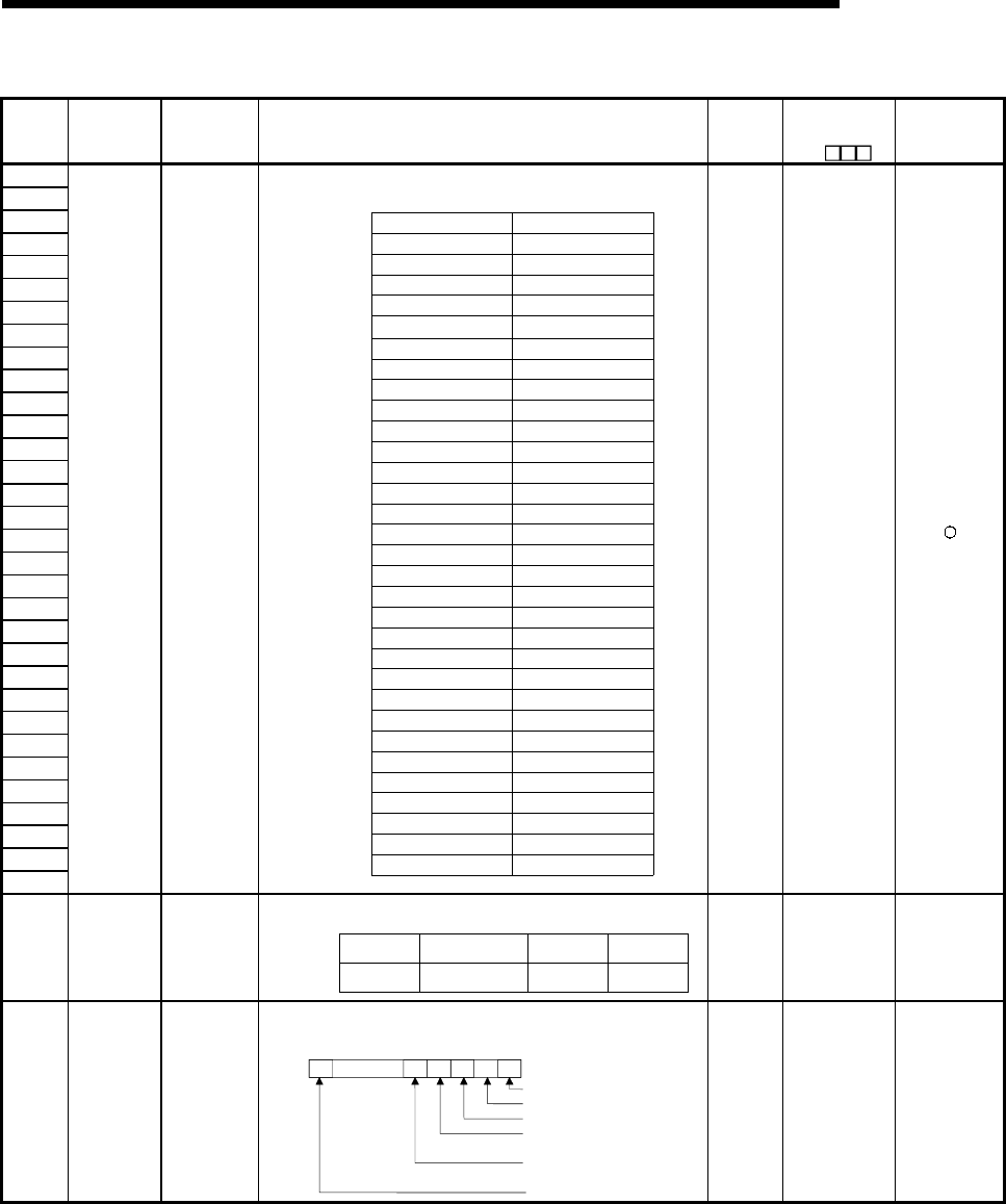
11 - 83 11 - 83
MELSEC-Q
11 TROUBLESHOOTING
Special Register List (Continued)
Number Name Meaning Explanation
Set by
(When
set)
Corresponding
ACPU
D9
Corresponding
CPU
SD738
SD739
SD740
SD741
SD742
SD743
SD744
SD745
SD746
SD747
SD748
SD749
SD750
SD751
SD752
SD753
SD754
SD755
SD756
SD757
SD758
SD759
SD760
SD761
SD762
SD763
SD764
SD765
SD766
SD767
SD768
SD769
Message
storage
Message
storage
• Stores the message designated by the MSG instruction.
SD738
SD739
SD740
SD741
SD742
SD743
1st character
B15 B8 B7 B0
SD744
SD745
SD746
SD747
SD748
SD749
SD750
SD751
SD752
SD753
SD754
SD755
SD756
SD757
SD758
SD759
SD760
SD761
SD762
SD763
SD764
SD765
SD766
SD767
SD768
SD769 64th character
2nd character
3rd character
4th character
5th character
6th character
7th character
8th character
9th character
10th character
11th character
12th character
13th character
14th character
15th character
16th character
17th character
18th character
19th character
20th character
21st character
22nd character
23rd character
24th character
25th character
26th character
27th character28th character
29th character
30th character
31st character
32nd character
33rd character
34th character
35th character
36th character
37th character
38th character
39th character
40th character
41st character
42nd character
43rd character
44th character
45th character
46th character
47th character
48th character
49th character
50th character
51st character
52nd character
53rd character
54th character
55th character
56th character
57th character
58th character
59th character
60th character
61st character
62nd character
63rd character
to to
S (During
execution) New
SD774
TO
SD775
PID limit
setting
0: Limit set
1: Limit not set
• Designate the limit for each PID loop as follows:
SD774
SD775
B15 B1 B0
Loop16
Loop32
Loop2
Loop18
Loop1
Loop17
to
to
U New QCPU
SD778
Refresh
processing
selection
when the
COM
instruction is
executed
Bits 0 to 4:
0:Do not
refresh
1:Refresh
F bit
0:Refresh
1:Do not
refresh
Selects whether or not the data is refreshed when the COM instruction
is executed.
1/0
I/O refresh
CC-Link refresh
MELSECNET/H refresh
Automatic refresh of intelligent
function modules
Automatic refresh of multi-CPU
shared memory
General data processing
SD778 01/01/01/01/01/0
b14 b5
to b4 b3 b2 b1 b0b15
U New
QCPU
Serial number
04012 or later
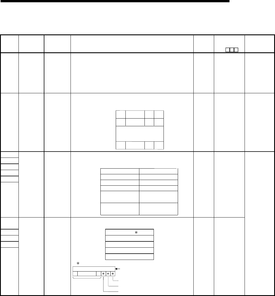
11 - 84 11 - 84
MELSEC-Q
11 TROUBLESHOOTING
Special Register List
(7) Debug
Number Name Meaning Explanation
Set by
(When
set)
Corresponding
ACPU
D9
Corresponding
CPU
SD780
Remaining
No. of
simultaneous
execution of
CC-Link
dedicated
instruction
0 to 32 • Stores the remaining number of simultaneous execution of the CC-
Link dedicated instructions. U New QnA
SD781
TO
SD793
Mask pattern
of IMASK
instruction
Mask pattern
• Stores the mask patterns masked by the IMASK instruction as
follows:
SD781
SD782
SD793
l63 l49 l48
l79
l255
l65
l241
l64
l240
B15 B0
B1
to
to
to
to
S (During
execution) New QCPU
SD806
SD807
SD808
SD809
SD810
SD811
Status latch
file name
Status latch
file name
• Stores file name (with extension) from point in time when status latch
was conducted as ASCII code.
SD806
SD807
SD808
SD809
SD810
SD811
First characterSecond character
Third characterFourth character
Fifth character
Sixth character
seventh character
Eighth character
B15 B8
to B7 B0
to
First character of
extension 2EH(.)
2nd character of
extension
Third character of
extension
S (During
execution) New
SD812 • Stores step number from point in time when status latch was
conducted.
SD813 SD812 Patterm
SD814 SD813 Block No.
SD815 SD814 Step No./transition No.
SD815 Sequence step No.(L)
SD816 Sequence step No.(H)
SD816
Status latch
step
Status latch
step
Contents of pattern data
0000
0123415 14
SFC transition designation present (1)/absent (0)
to
to
(Bit number)
(Not in use) SFC block designation present (1)/absent (0)
SFC block designation present (1)/absent (0)
S (During
execution)
D9055 format
change
QnA
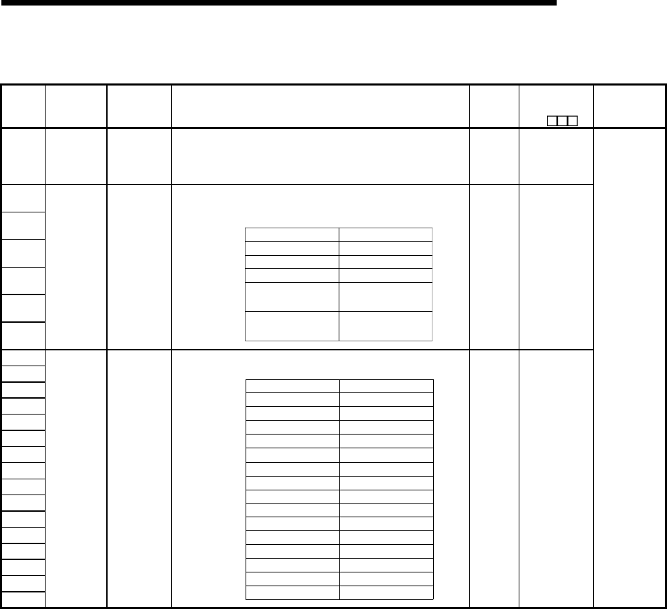
11 - 85 11 - 85
MELSEC-Q
11 TROUBLESHOOTING
Special Register List
(8) Latch area
Number Name Meaning Explanation
Set by
(When
set)
Corresponding
ACPU
D9
Corresponding
CPU
SD900
Drive where
power was
interrupted
Access file
drive number
during power
loss
• Stores drive number if file was being accessed during power loss. S (Status
change) New
SD901
SD902
SD903
SD904
SD905
SD906
File name
active during
power loss
Access file
name during
power loss
• Stores file name (with extension) in ASCII code if file was being
accessed during power loss.
SD901
SD902
SD903
SD904
SD905
SD906
B15 B8 B7 B0
1st character
2nd character
3rd character
4th character
5th character6th character
7th character
8th character
to to
1st character of
extension 2EH(.)
2nd character of
extension
3rd character of
extension
S (Status
change) New
SD910
SD911
SD912
SD913
SD914
SD915
SD916
SD917
SD918
SD919
SD920
SD921
SD922
SD923
SD924
SD925
RKEY input RKEY input
• Stored in sequence that PU key code was entered.
SD910
SD911
SD912
SD913
SD914
SD915
B15 B8 B7 B0
SD916
SD917
SD918
SD919
SD920
SD921
SD922
SD923
SD924
SD925
1st character
2nd character
3rd character4th character
5th character6th character
7th character
8th character
9th character
10th character
11th character
12th character
13th character
14th character
15th character
16th character
17th character
18th character
19th character
20th character
21st character
22nd character
23rd character
24th character
25th character
26th character
27th character
28th character
29th character
30th character
31st character
32nd character
to to
S (During
execution) New
QnA
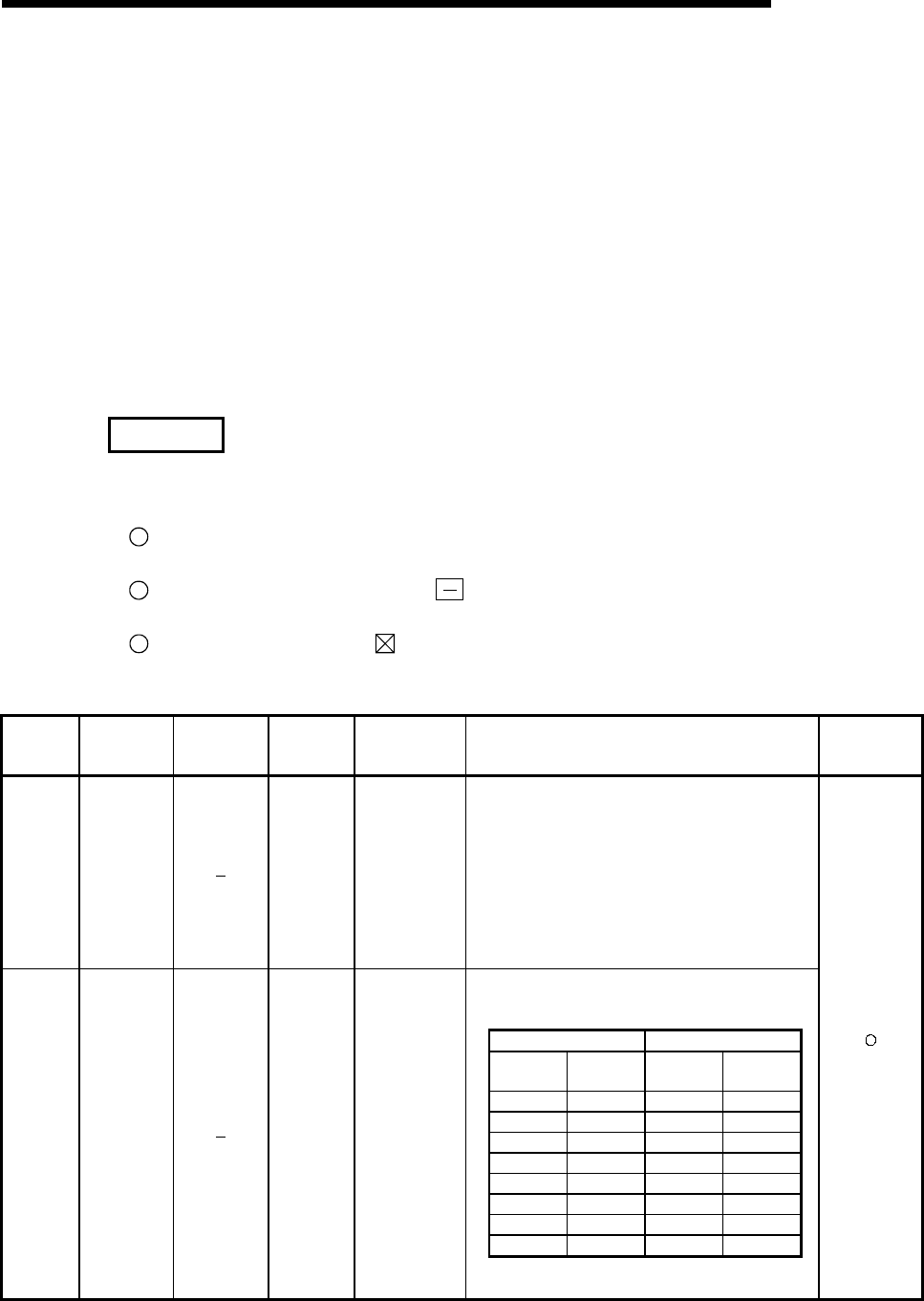
11 - 86 11 - 86
MELSEC-Q
11 TROUBLESHOOTING
(9) A to Q/QnA conversion correspondences
ACPU special registers D9000 to D9255 correspond to the special registers SD1000 to
SD1255 after A-series to the Q/QnA-series conversion.
These special registers are all set by the system, and users cannot use them to set program
data.
Users who need to set data with these registers should edit the special registers for the
Q/QnA.
However, before conversion users could set data at special registers D9200 to D9255 only,
and after conversion users can also set data at registers 1200 to 1255.
For more detailed information concerning the contents of the ACPU special registers, see the
individual CPU users manual, and the MELSECNET and MELSECNET/B data link system
reference manual.
REMARK
Supplemental explanation on "Special Register for Modification" column
1 For the device numbers for which a special register for modification is specified, modify it to
the special register for QCPU/QnACPU.
2 For the device numbers for which is specified, special register after conversion can be
used.
3 Device numbers for which is specified do not function for QCPU/QnACPU.
Special Register List
ACPU
Special
Conversion
Special
Register after
Conversion
Special
Register for
Modification
Name Meaning Details Corresponding
CPU
D9000 SD1000 Fuse blown
Number of
module with
blown fuse
• When fuse blown modules are detected, the lowest
number of detected units is stored in hexadecimal.
(Example: When fuses of Y50 to 6F output modules have
blown, "50" is stored in hexadecimal)
To monitor the number by peripheral devices, perform
monitor operation given in hexadecimal.
(Cleared when all contents of SD1100 to SD1107 are reset
to 0.)
• Fuse blow check is executed also to the output modules of
remote I/O stations.
• Stores the module numbers corresponding to setting
switch numbers or base unit slot numbers when fuse blow
occurred.
I/O module for A0J2 Extension base unit
Setting
switch Stored data Base unit
slot No. Stored data
0 1 0 5
1 2 1 6
2 3 2 7
3 4 3 8
4 5
5 6
6 7
7 8
D9001 SD1001 Fuse blown
Number of
module with
blown fuse
• For remote I/O station, value of (module I/O number/10H)
+ 1 is stored.
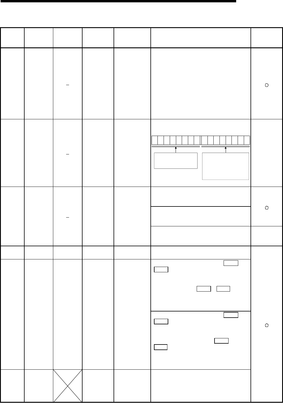
11 - 87 11 - 87
MELSEC-Q
11 TROUBLESHOOTING
Special Register List (Continued)
ACPU
Special
Conversion
Special
Register after
Conversion
Special
Register for
Modification
Name Meaning Details Corresponding
CPU
D9002 SD1002
I/O module
verification error
I/O module
verification error
module number
• If I/O modules, of which data are different from data
entered, are detected when the power is turned on,
the first I/O number of the lowest number unit among
the detected units is stored in hexadecimal. (Storing
method is the same as that of SD1000.) To monitor
the number by peripheral devices, perform monitor
operation given in hexadecimal.
(Cleared when all contents of SD1116 to SD1123 are
reset to 0.)
• I/O module verify check is executed also to the
modules of remote I/O terminals.
D9004 SD1004
MINI link master
module errors
Error detection
state
• Stores the MINI(S3) link error detection status in the
mounted MELSECNET/MINI-S3 master module.
B15 B8 B7 B0
876543218
7654321
Bits which correspond to the signals of
A(1S)J71PT32(S3), shown below, are
turned on as the signals are turned on.
· Hardware error (X0/X20)
· MINI(S3) link error datection (X6/X26)
· MINI(S3) link communication error
(X7/X27)
to to
On the PLC CPU and
A(1S)J71PT32(S3) side, the bit
corresponding to the
A(1S)J71PT32(S3) that cannot
make data communication turns ON.
QnA
• Turned ON if instantaneous power failure of within
20ms occurs when AC power supply module is used,
and reset when power is switched OFF, then ON.
• Turned ON if instantaneous power failure of within
10ms occurs when DC power supply module is used,
and reset when power is switched OFF, then ON.
D9005 SD1005
AC DOWN
counter
Number of times for
AC DOWN
• Turned ON if instantaneous power failure of within
1ms occurs when DC power supply module is used,
and reset when power is switched OFF, then ON.
QnA
D9008 SD1008 SD0 Self-diagnosis
error
Self-diagnosis error
code
• When error is found as a result of self-diagnosis, error
code is stored in BIN code.
• When one of F0 to 2047 is turned on by OUT F or
SET F , the F number, which has been detected
earliest among the F numbers which have turned on,
is stored in BIN code.
• SD62 can be cleared by RST F or LEDR
instruction.
If another F number has been detected, the clearing of
SD62 causes the next number to be stored in SD62.
D9009 SD1009 SD62 Annunciator
detection
F number at which
external failure has
occurred
• When one of F0 to 2047 is turned on by OUT F or
SET F , the F number, which has been detected
earliest among the F numbers which have turned on,
is stored in BIN code.
• SD62 can be cleared by executing RST F or
LEDR instruction or moving INDICATOR RESET
switch on CPU front to ON position. If another F
number has been detected, the clearing of SD62
causes the nest number to be stored in SD62.
D9010 SD1010 Error step
Step number at
which operation
error has occurred.
• When operation error has occurred during execution
of application instruction, the step number, at which
the error has occurred, is stored in BIN code.
Thereafter, each time operation error occurs, the
contents of SD1010 are renewed.
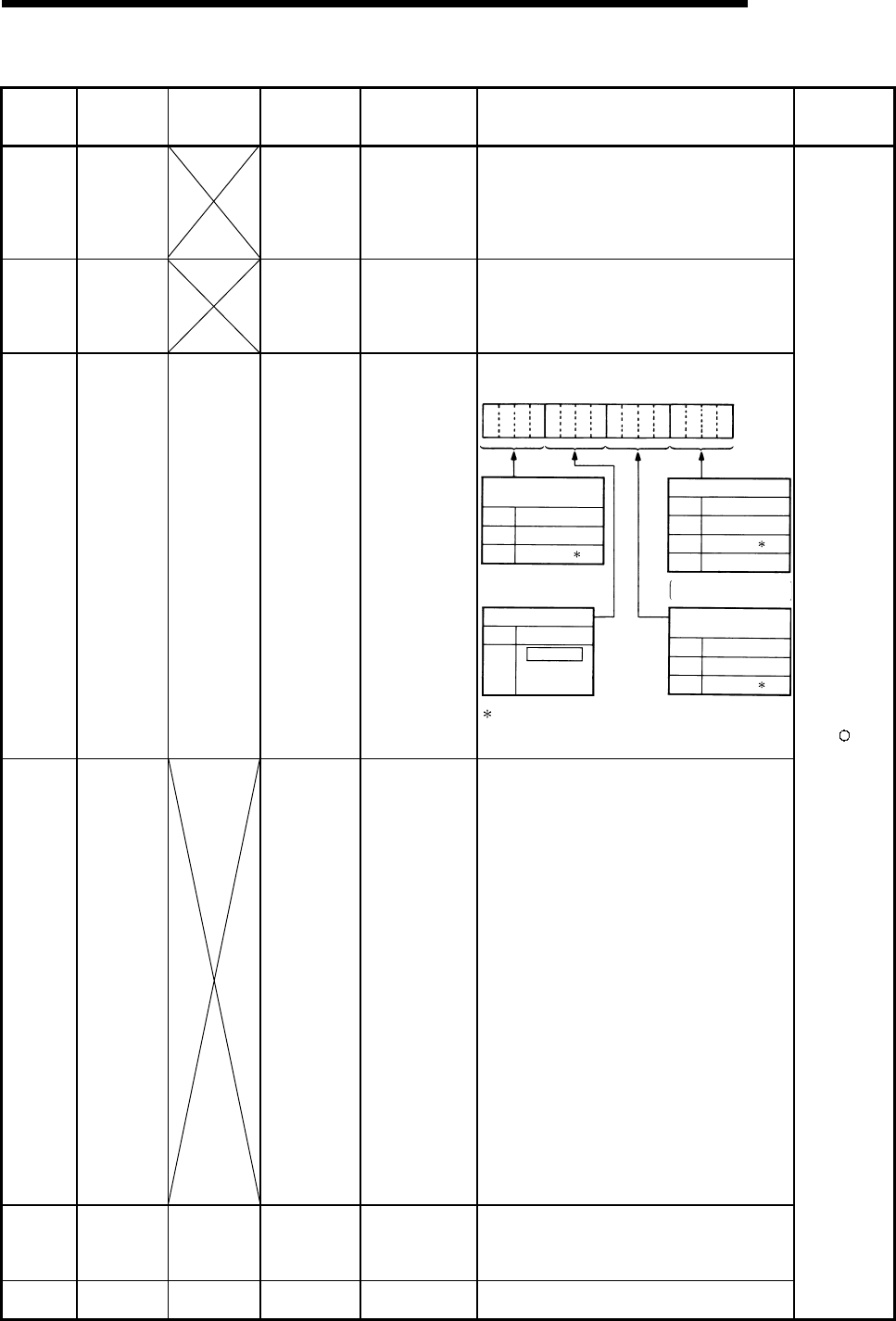
11 - 88 11 - 88
MELSEC-Q
11 TROUBLESHOOTING
Special Register List (Continued)
ACPU
Special
Conversion
Special
Register after
Conversion
Special
Register for
Modification
Name Meaning Details Corresponding
CPU
D9011 SD1011 Error step
Step number at
which operation
error has occurred.
• When operation error has occurred during execution
of application instruction, the step number, at which
the error has occurred, is stored in BIN code. Since
storage into SD1011 is made when SM1011 changes
from off to on, the contents of SD1011 cannot be
renewed unless SM1011 is cleared by user program.
D9014 SD1014 I/O control mode I/O control mode
number
• The I/O control mode set is returned in any of the
following numbers:
0. Both input and output in direct mode
1. Input in refresh mode, output in direct mode
3. Both input and output in refresh mode
D9015 SD1015 SD203
Operating status
of CPU
Operating status of
CPU
• The operation status of CPU as shown below are
stored in SD203.
CPU key switch
Remains the same in
remote RUN/STOP mode.
0RUN
1STOP
2
3STEP RUN
Remote RUN/STOP
by parameter setting
PAUSE 1
Remote RUN/STOP
by computer
instruction
execution
STOP
Status in program
Except below
B15 B12 B11 B8 B7 B4 B3 B0
0RUN
1STOP
2PAUSE 1
0RUN
1STOP
2PAUSE 1
0
1
to to to to
1 When the CPU module is in RUN mode and
SM1040 is off, the CPU remains in RUN mode if
changed to PAUSE mode.
D9016 SD1016 Program
number
0: Main program
(ROM)
1: Main program
(RAM)
2: Subprogram 1
(RAM)
3: Subprogram 2
(RAM)
4: Subprogram 3
(RAM)
5: Subprogram 1
(ROM)
6: Subprogram 2
(ROM)
7: Subprogram 3
(ROM)
8: Main program
(E2PROM)
9: Subprogram 1
(E2PROM)
A: Subprogram 2
(E2PROM)
B: Subprogram 3
(E2PROM)
• Indicates which sequence program is run presently.
One value of 0 to B is stored in BIN code.
D9017 SD1017 SD520 Scan time Minimum scan time
(10 ms units)
• If scan time is smaller than the content of SD520, the
value is newly stored at each END. Namely, the
minimum value of scan time is stored into SD520 in
BIN code.
D9018 SD1018 SD524 Scan time Scan time
(10 ms units)
• Scan time is stored in BIN code at each END and
always rewritten.
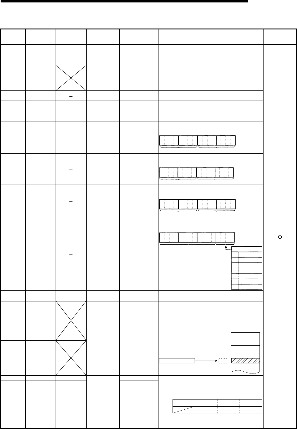
11 - 89 11 - 89
MELSEC-Q
11 TROUBLESHOOTING
Special Register List (Continued)
ACPU
Special
Conversion
Special
Register after
Conversion
Special
Register for
Modification
Name Meaning Details Corresponding
CPU
D9019 SD1019 SD526 Scan time Maximum scan
time (10 ms units)
• If scan time is larger than the content of SD526, the
value is newly stored at each END. Namely, the
maximum value of scan time is stored into SD526 in
BIN code.
D9020 SD1020 Constant scan
Constant scan time
(User sets in 10 ms
units)
• Sets the interval between consecutive program starts
in multiples of 10 ms.
0: No setting
1 to 200: Set. Program is executed at intervals of
(set value) × 10 ms.
D9021 SD1021 Scan time Scan time
(1 ms units)
• Scan time is stored and updated in BIN code after
every END.
D9022 SD1022 SD412 1 second
counter
Count in units of
1sec.
• When the PC CPU starts running, it starts counting 1
every second.
• Count repeats changing from 0 to 32767 to -32768 to
0.
D9025 SD1025 Clock data Clock data
(year, month)
• Year (lower 2 digits) and month are stored into
SD1025 in BCD code as shown below.
B15 B12 B11 B8 B7 B4 B3 B0
Example:
1987, July
H8707
Year Month
to to to to
D9026 SD1026 Clock data Clock data
(day, hour)
• Day and hour are stored into SD1026 in BCD code as
shown below.
B15 B12 B11 B8 B7 B4 B3 B0
Day Hour
Example
31th, 10 o'clock
H3110
to to to to
D9027 SD1027 Clock data Clock data
(minute, second)
• Minute and second are stored into SD1027 in BCD
code as shown below.
B15 B12 B11 B8 B7 B4 B3 B0
Minute Second
Example:
35 minutes,
48 seconds
H3548
to to to to
D9028 SD1028 Clock data Clock data
(day of week)
• Day of week is stored into SD1028 in BCD code as
shown below.
B15 B12 B11 B8 B7 B4 B3 B0 Example:
Friday
H0005
0 must be set. Day of the week
0
1
2
3
4
5
6
Sunday
Monday
Tuesday
Wednesday
Thursday
Friday
Saturday
to to to to
D9035 SD1035 SD648 Extension file
register Use block No. • Stores the block No. of the extension file register
being used in BCD code.
D9036 SD1036
D9037 SD1037
Extension file
registerfor
designation of
device number
Device number
when individual
devices from
extension file
register are directly
accessed
• Designate the device number for the extension file
register for direct read and write in 2 words at SD1036
and SD1037 in BIN data.
Use consecutive numbers beginning with R0 of block
No. 1 to designate device numbers.
SD1036,SD1037
0
16383
16384
Block No.2 area
Device No. (BIN data)
Exetension file register
Block No.1 area
to
to
to
D9038 SD1038 SD207 Priorities 1 to 4
D9039 SD1039 SD208
LED display
priority ranking Priorities 5 to 7
• Sets priority of ERROR LEDs which illuminate (or
flicker) to indicate errors with error code numbers.
• Configuration of the priority setting areas is as shown
below.
SD207
SD208
B15 B12 B11 B8 B7 B4 B3 B0
Priority 4 Priority 3 Priority 2 Priority 1
Priority 5
Priority 6
Priority 7
to to to to
• For details, refer to the applicable CPUs User’s
Manual and the ACPU Programming manual
(Fundamentals).
11 - 90 11 - 90
MELSEC-Q
11 TROUBLESHOOTING
Special Register List (Continued)
ACPU
Special
Conversion
Special
Register after
Conversion
Special
Register for
Modification
Name Meaning Details Corresponding
CPU
D9044 SD1044 For sampling
trace
Step or time during
sampling trace
• When SM803 is turned ON/OFF by peripheral device
to activate sampling trace STRA , STRAR , value
stored in SD1044 is used as sampling trace condition.
For scan ....... 0
For time ....... Time (10ms increments)
Value is stored into SD1044 in BIN code.
D9049 SD1049 Work area for
SFC
Extension file
register block No.
used as SFC
program execution
work area
• Stores the block number of the expansion file register
which is used as the work area for the execution of a
SFC program in a binary value.
• Stores "0" if an empty area of 16K bytes or smaller,
which cannot be expansion file register No. 1, is used
or if SM320 is OFF.
D9050 SD1050 SFC program
error number
Error code
generated by SFC
program
• Stores code numbers of errors occurred in the SFC
program in BIN code.
0: No error
80: SFC program parameter error
81: SFC code error
82: Number of steps of simultaneous execution
exceeded
83: Block start error
84: SFC program operation error
D9051 SD1051 Error block
Block number
where error
occurred
• Stores the block number in which an error occurred in
the SFC program in BIN code.
In the case of error 83 the starting block number is
stored.
D9052 SD1052 Error step Step number where
error occurred
• Stores the step number in which error 84 occurred in
the SFC program in BIN code.
Stores "0" when errors 80, 81 and 82 occurred.
Stored the block starting step number when error 83
occurred.
D9053 SD1053 Error transition
Transition condition
number where error
occurred
• Stores the transfer condition number in which error 84
occurred in the SFC program in BIN code.
Stored "0" when errors 80, 81, 82 and 83 occurred.
D9054 SD1054 Error sequence
step
Sequence step
number where error
occurred
• Stores the sequence step number of transfer condition
and operation output in which error 84 occurred in the
SFC program in BIN code.
D9055 SD1055 SD812
Status latch
execution step
No.
Status latch
execution step No.
• Stores the step number when status latch is executed.
• Stores the step number in a binary value if status latch
is executed in a main sequence program.
• Stores the block number and the step number if status
latch is executed in a SFC program.
Block No.
(BIN)
Step No.
(BIN)
Higher 8 bits Lower 8 bits
D9060 SD1060 SD392 Software version
Software version of
internal software
• Stores the software version of the internal system in
ASCII code.
Higher byte Lower byte
The data in the lower byte
position is indefinite.
The software version is stored
in the higher byte position.
For version "A", for example, "41H" is stored.
Note: The software version of the initial system may
differ from the version indicated by the version
information printed on the rear of the case.
QnA
D9072 SD1072
PLC
communications
check
Data check of serial
communication
module
• In the self-loopback test of the serial communication
module, the serial communication module writes/reads
data automatically to make communication checks.
D9081 SD1081 SD714
Number of
empty blocks in
communications
request
registrtion area
0 to 32
• Stores the number of empty blocks in the
communication request registration area to the remote
terminal module connected to the MELSECNET/MINI-
S3 master unit, A2C or A52G.
QnA
11 - 91 11 - 91
MELSEC-Q
11 TROUBLESHOOTING
Special Register List (Continued)
ACPU
Special
Conversion
Special
Register after
Conversion
Special
Register for
Modification
Name Meaning Details Corresponding
CPU
D9085 SD1085
Register for
setting time
check value
1s to 65535s
• Sets the time check time of the data link instructions
(ZNRD, ZNWR) for the MELSECNET/10.
• Setting range: 1 s to 65535 s (1 to 65535)
• Setting unit: s
• Default value: 10 s (If 0 has been set, default
10 s is applied)
D9090 SD1090
Microcomputer
subroutine input
data area head
device No.
According to
corresponding
microcomputer
package
• For details, refer to the manual of each microcomputer
program package.
D9091 SD1091 Detailed error
code
Self-diagnosis
detailed error code • Stores the detail code of cause of an instruction error.
D9094 SD1094 SD251
Head I/O
number for
replacement
Head I/O number
for replacement
• Stores upper 2 digits of the head I/O address of I/O
modules to be loaded or unloaded during online mode
in BIN code.
Example) Input module X2F0 → H2F
D9100 SD1100
D9101 SD1101
D9102 SD1102
D9103 SD1103
D9104 SD1104
D9105 SD1105
D9106 SD1106
D9107 SD1107
Fuse blown
module
Bit pattern in units
of 16 points,
indicating the
modules whose
fuses have blown
• Output module numbers (in units of 16 points), of
which fuses have blown, are entered in bit pattern.
(Preset output unit numbers when parameter setting
has been performed.)
15 14 13 12 11 10 9 8 7 6 5 4 3 2 1 0
00000000
1
(Y80)
000000
0000000000000000
00000000000000 1
Y7
B0
S
D1100
S
D1101
S
D1107
1
(YCO)
Indicates fuse blow.
1
Y7
30
• Fuse blow check is executed also to the output
module of remote I/O station.
(If normal status is restored, clear is not performed.
Therefore, it is required to perform clear by user
program.)
D9108 SD1108
D9109 SD1109
D9110 SD1110
D9111 SD1111
D9112 SD1112
D9113 SD1113
D9114 SD1114
Step transfer
monitoring timer
setting
Timer setting valve
and the F number
at time out
• Sets value for the step transfer monitoring timer and
the number of F which turns on when the monitoring
timer timed out.
Timer setting
(1 to 255 s in seconds)
F number setting
b15 b8 b7 b0to to
(By turning on any of SM1108 to SM1114, the
monitoring timer starts. If the transfer condition
following a step which corresponds to the timer is not
established within set time, set annunciator (F) is
tuned on.)
D9116 SD1116
D9117 SD1117
D9118 SD1118
D9119 SD1119
D9120 SD1120
D9121 SD1121
D9122 SD1122
D9123 SD1123
I/O module
verification error
Bit pattern, in units
of 16 points,
indicating the
modules with
verification errors.
• When I/O modules, of which data are different from
those entered at power-on, have been detected, the
I/O unit numbers (in units of 16 points) are entered in
bit pattern. (Preset I/O unit numbers when parameter
setting has been performed.)
15 14 13 12 11 10 9 8 7 6 5 4 3 2 1 0
0000000000000
000000000000000
00000000000000 1
XY
100
SD1116
SD1117
SD1123
1
XY
0
1
XY
100
0
00
Indicates I/O module verify error.
• I/O module verify check is executed also to remote I/O
station modules.
(If normal status is restored, clear is not performed.
Therefore, it is required to perform clear by user
program.)
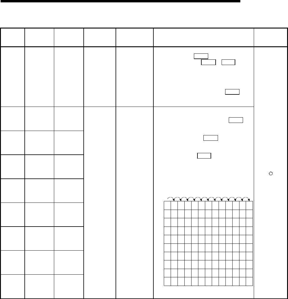
11 - 92 11 - 92
MELSEC-Q
11 TROUBLESHOOTING
Special Register List (Continued)
ACPU
Special
Conversion
Special
Register after
Conversion
Special
Register for
Modification
Name Meaning Details Corresponding
CPU
D9124 SD1124 SD63
Annunciator
detection
quantity
Annunciator
detection quantity
• When one of F0 to 2047 (F0 to 2047 for AuA and
AnU) is turned on by SET F 1 is added to the
contents of SD63. When RST F or LEDR
instruction is executed, 1 is subtracted from the
contents of SD63. (If the INDICATOR RESET switch
is provided to the CPU, pressing the switch can
execute the same processing.)
• Quantity, which has been turned on by SET F is
stored into SD63 in BIN code. The value of SD63 is
maximum 8.
D9125 SD1125 SD64
D9126 SD1126 SD65
D9127 SD1127 SD66
D9128 SD1128 SD67
D9129 SD1129 SD68
D9130 SD1130 SD69
D9131 SD1131 SD70
D9132 SD1132 SD71
Annunciator
detection
number
Annunciator
detection number
• When any of F0 to 2047 is turned ON by SET F , F
numbers turned ON sequentially are registered into
D9125 - D9132.
F numbers turned OFF by RST F are deleted from
D9125 - D9132, and move to data registers
subsequent to the ones that stored deleted F
numbers. Execution of LEDR instruction shifts up
SD64 - SD71 contents one place. (When CPU has
INDICATOR RESET switch, pressing that switch
performs the same processing.) When there are eight
annunciator numbers detected, the ninth number is
not stored into SD64 - SD71 if detected.
0 505050505050505050505099
0
0 5050505050505050505099
0 2525999999999999999915
1232345678 88
50
0
0 99 1515151515151570
00 0
0 70707070707065
00 000
0 65656565653800 0000
0 38383838
110
00 0000
0
0 110 110 110 151
00 0000
0
0 151 151 210
00 0000
0
0
00
S
D62
S
D63
S
D64
S
D65
S
D66
S
D67
S
D68
S
D69
S
D70
S
D71
SET
F50
SET
F25
SET
F99
RST
F25
SET
F15
SET
F70
SET
F65
SET
F38
SET
F110
SET
F151
SET
F210 LEDR
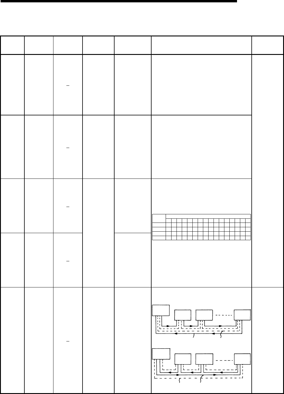
11 - 93 11 - 93
MELSEC-Q
11 TROUBLESHOOTING
Special Register List
(10) Special register list dedicated for QnA
ACPU
Special
Conversion
Special
Register after
Conversion
Special
Register for
Modification
Name Meaning Details Corresponding
CPU
Stores the execution result of the ZNRD (word device
read) instruction
• ZNRD instruction setting fault: Faulty setting of the
ZNRD instruction
constant, source,
and/or destination
• Corresponding station error: One of the stations is
not communicating.
D9200 SD1200
ZNRD
(LRDP for
ACPU)
processing
results
0: Normal end
2: ZNRD instruction
setting fault
3: Error at relevant
station
4: Relevant station
ZNRD execution
disabled • ZNRD cannot be executed in
the corresponding station:
The specified station is
a remote I/O station.
Stores the execution result of the ZNWR (word device
write) instruction.
• LWTP instruction setting fault: Faulty setting of the
ZNWR instruction
constant, source,
and/or destination.
• Corresponding station error: One of the stations is
not communicating.
D9201 SD1201
ZNWR
(LWTP for
ACPU)
processing
results
0: Normal end
2: ZNWR
instruction setting
fault
3: Error at relevant
station
4: Relevant station
ZNWR execution
disabled • ZNWR cannot be executed in
the corresponding station:
The specified station is
a remote I/O station.
D9202 SD1202
Stores conditions
for up to numbers 1
to 16
D9203 SD1203
Local station link
type
Stores conditions
for up to numbers
17 to 32
Stores whether the slave station corresponds to
MELSECNET or MELSECNET II.
• Bits corresponding to the MELSECNET II stations
become "1."
• Bits corresponding to the MELSECNET stations or
unconnected become "0."
SD1202
SD1203
SD1241
SD1242
b15 b14 b13 b12 b11 b10 b9 b8 b7 b6 b5 b4 b3 b2 b1 b0
L16 L15 L14 L13 L12 L11
L32 L31 L30 L29 L28 L27
L48 L47 L46 L45 L44 L43
L64 L63 L62 L61 L60 L59
L26
L42
L58
L25
L41
L57
L24
L40
L56
L23
L39
L55
L22
L38
L54
L21
L37
L53
L20
L36
L52
L19
L35
L51
L18
L34
L50
L17
L33
L49
L10 L9 L8 L7 L6 L5 L4 L3 L2 L1
Bit
Device
number
• If a local station goes down during the operation, the
contents before going down are retained.
Contents of SD1224 to SD1227 and SD1228 to
SD1231 are ORed. If the corresponding bit is "0", the
corresponding bit of the special register above
becomes valid.
• If the own (master) station goes down, the contents
before going down are also retained.
QnA
D9204 SD1204 Link status
0: Forward loop,
during data link
1: Reverse loop,
during data link
2: Loopback
implemented in
forward/reverse
directions
3: Loopback
implemented
only in forward
direction
4: Loopback
implemented
only inreverse
direction
5: Data link
disabled
Stores the present path status of the data link.
• Data link in forward loop
Master
station Station 1 Station 2 Station n
Forward loop Reverse loop
• Data link in reverse loop
Master
station Station 1 Station 2 Station n
Forward loop Reverse loop
QnA
11 - 94 11 - 94
MELSEC-Q
11 TROUBLESHOOTING
Special Register List (Continue)
ACPU
Special
Conversion
Special
Register after
Conversion
Special
Register for
Modification
Name Meaning Details Corresponding
CPU
D9204 SD1204 Link status
0: Forward loop,
during data link
1: Reverse loop,
during data link
2: Loopback
implemented in
forward/reverse
directions
3: Loopback
implemented only
in forward
direction
4: Loopback
implemented only
inreverse direction
5: Data link disabled
• Loopback in forward/reverse loops
Master
station Station 1 Station 2 Station 3 Station n
F
orward loopback Reverse loopback
• Loopback in forward loop only
Master
station Station 1 Station 2 Station 3 Station n
Forward loopback
• Loopback in reverse loop only
Master
station Station 1 Station 2 Station 3 Station n
Reverse loopback
D9205 SD1205
Station
implementing
loopback
Station that
implemented forward
loopback
D9206 SD1206
Station
implementing
loopback
Station that
implemented reverse
loopback
Stores the local or remote I/O station number at which
loopback is being executed.
Master
station Station 1 Station 2 Station 3 Station n
Forward loopback Reverse loopback
In the example of above figure, "1" is stored into
SD1205 and "3" into SD1206. If data link returns to
normal status (data link in forward loop), values stored
into SD1205, SD1206 do not return to "0". To return
them to "0", therefore, sequence program must be
used or reset operation performed.
D9210 SD1210 Number of
retries
Stored as cumulative
value
Stores the number of retry times due to transmission
error.
Count stops at maximum of "FFFFH" .
RESET to return the count to 0.
D9211 SD1211 Number of times
loop selected
Stored as cumulative
value
Stores the number of times the loop line has been
switched to reverse loop or loopback.
Count stops at maximum of "FFFFH".
RESET to return the count to 0.
QnA
D9212 SD1212 Local station
operation status
Stores conditions for
up to numbers 1 to
16
D9213 SD1213 Local station
operation status
Stores conditions for
up to numbers 17 to
32
D9214 SD1214 Local station
operation status
Stores conditions for
up to numbers 33 to
48
D9215 SD1215 Local station
operation status
Stores conditions for
up to numbers 49 to
64
Stores the local station numbers which are in STOP or
PAUSE mode.
SD1212
SD1213
SD1214
SD1215
b15 b14 b13 b12 b11 b10 b9 b8 b7 b6 b5 b4 b3 b2 b1 b0
L16 L15 L14 L13 L12 L11
L32 L31 L30 L29 L28 L27
L48 L47 L46 L45 L44 L43
L64 L63 L62 L61 L60 L59
L26
L42
L58
L25
L41
L57
L24
L40
L56
L23
L39
L55
L22
L38
L54
L21
L37
L53
L20
L36
L52
L19
L35
L51
L18
L34
L50
L17
L33
L49
L10L9L8L7L6L5L4L3L2L1
Bit
Device
number
When a local station is switched to STOP or PAUSE
mode, the bit corresponding to the station number in
the register becomes "1".
Example: When station 7 switches to STOP mode,
bit 6 in SD1212 becomes "1" , and when
SD1212 is monitored, its value is "64
(40H)".
QnA
11 - 95 11 - 95
MELSEC-Q
11 TROUBLESHOOTING
Special Register List (Continue)
ACPU
Special
Conversion
Special
Register after
Conversion
Special
Register for
Modification
Name Meaning Details Corresponding
CPU
D9216 SD1216
Stores conditions
for up to numbers
1 to 16
D9217 SD1217
Stores conditions
for up to numbers
17 to 32
D9218 SD1218
Stores conditions
for up to numbers
33 to 48
D9219 SD1219
Local station
error detect
status
Stores conditions
for up to numbers
49 to 64
Station numbers of local stations that have detected
errors are stored into corresponding data register bits as
indicated below.
SD1216
SD1217
SD1218
SD1219
b15 b14 b13 b12 b11 b10 b9 b8 b7 b6 b5 b4 b3 b2 b1 b0
L16 L15 L14 L13 L12 L11
L32 L31 L30 L29 L28 L27
L48 L47 L46 L45 L44 L43
L64 L63 L62 L61 L60 L59
L26
L42
L58
L25
L41
L57
L24
L40
L56
L23
L39
L55
L22
L38
L54
L21
L37
L53
L20
L36
L52
L19
L35
L51
L18
L34
L50
L17
L33
L49
L10L9L8L7L6L5L4L3L2L1
Bit
Device
number
If a local station detects an error, the bit corresponding to
the station number becomes "1".
Example: When station 6 and 12 detect an error, bits 5
and 11 in SD1216 become "1", and when
SD1216 is monitored, its value is "2080
(820H)".
D9220 SD1220
Stores conditions
for up to numbers
1 to 16
D9221 SD1221
Stores conditions
for up to numbers
17 to 32
D9222 SD1222
Stores conditions
for up to numbers
33 to 48
D9223 SD1223
Local station
parameters
non-conforming;
remote I/O
station I/O
allocation error
Stores conditions
for up to numbers
49 to 64
Stores the local station numbers that have mismatches
between the parameters of the master station of tier three
and those of the master station in tier two in the three tier
system or the remote I/O station numbers that have
incorrect I/O assignment, as shown below in
correspondence with the data register bits.
SD1220
SD1221
SD1222
SD1223
b15 b14 b13 b12 b11 b10 b9 b8 b7 b6 b5 b4 b3 b2 b1 b0
L16 L15 L14 L13 L12 L11
L32 L31 L30 L29 L28 L27
L48 L47 L46 L45 L44 L43
L64 L63 L62 L61 L60 L59
L26
L42
L58
L25
L41
L57
L24
L40
L56
L23
L39
L55
L22
L38
L54
L21
L37
L53
L20
L36
L52
L19
L35
L51
L18
L34
L50
L17
L33
L49
L10L9L8L7L6L5L4L3L2L1
Bit
Device
number
If a local station acting as the master station of tier three
detects a parameter error or a remote station contains an
invalid I/O assignment, the bit corresponding to the
station number becomes "1".
Example: When local station 5 and remote I/O station
14 detect an error, bits 4 and 13 in SD1220
become "1" , and when SD1220 is monitored,
its value is "8208 (2010H) " .
D9224 SD1224
Stores conditions
for up to numbers
1 to 16
D9225 SD1225
Stores conditions
for up to numbers
17 to 32
D9226 SD1226
Stores conditions
for up to numbers
33 to 48
D9227 SD1227
Local station
and remote I/O
station initial
communications
underway
Stores conditions
for up to numbers
49 to 64
Stores the local or remote station numbers while they are
communicating the initial data with their relevant master
station.
SD1224
SD1225
SD1226
SD1227
b15 b14 b13 b12 b11 b10 b9 b8 b7 b6 b5 b4 b3 b2 b1 b0
L/R
16 L/R
15 L/R
14 L/R
13 L/R
12 L/R
11 L/R
10 L/R
9L/R
8L/R
7L/R
6L/R
5L/R
4L/R
3L/R
2L/R
1
L/R
32 L/R
31 L/R
30 L/R
29 L/R
28 L/R
27 L/R
26 L/R
25 L/R
24 L/R
23 L/R
22 L/R
21 L/R
20 L/R
19 L/R
18 L/R
17
L/R
48 L/R
47 L/R
46 L/R
45 L/R
44 L/R
43 L/R
42 L/R
41 L/R
40 L/R
39 L/R
38 L/R
37 L/R
36 L/R
35 L/R
34 L/R
33
L/R
64 L/R
63 L/R
62 L/R
61 L/R
60 L/R
59 L/R
58 L/R
57 L/R
56 L/R
55 L/R
54 L/R
53 L/R
52 L/R
51 L/R
50 L/R
49
Bit
Device
number
The bit corresponding to the station number which is
currently communicating the initial settings becomes "1" .
Example: When stations 23 and 45 are communicating,
bit 6 of SD1225 and bit 12 of SD1226
become "1", and when SD1225 is monitored,
its value is "64 (40H)", and when SD1226 is
monitored, its value is "4096 (1000H)"
D9228 SD1228
Stores conditions
for up to numbers
1 to 16
D9229 SD1229
Stores conditions
for up to numbers
17 to 32
D9230 SD1230
Stores conditions
for up to numbers
33 to 48
D9231 SD1231
Local station
and remote I/O
station error
Stores conditions
for up to numbers
49 to 64
Stores the local or remote station numbers which are in
error.
SD1228
SD1229
SD1230
SD1231
b15 b14 b13 b12 b11 b10 b9 b8 b7 b6 b5 b4 b3 b2 b1 b0
L/R
16 L/R
15 L/R
14 L/R
13 L/R
12 L/R
11 L/R
10 L/R
9L/R
8L/R
7L/R
6L/R
5L/R
4L/R
3L/R
2L/R
1
L/R
32 L/R
31 L/R
30 L/R
29 L/R
28 L/R
27 L/R
26 L/R
25 L/R
24 L/R
23 L/R
22 L/R
21 L/R
20 L/R
19 L/R
18 L/R
17
L/R
48 L/R
47 L/R
46 L/R
45 L/R
44 L/R
43 L/R
42 L/R
41 L/R
40 L/R
39 L/R
38 L/R
37 L/R
36 L/R
35 L/R
34 L/R
33
L/R
64 L/R
63 L/R
62 L/R
61 L/R
60 L/R
59 L/R
58 L/R
57 L/R
56 L/R
55 L/R
54 L/R
53 L/R
52 L/R
51 L/R
50 L/R
49
Bit
Device
number
The bit corresponding to the station number with the error
becomes "1" .
Example: When local station 3 and remote I/O station
14 have an error, bits 2 and 13 of SD1228
become "1", and when SD1228 is monitored,
its value is "8196 (2004H)".
QnA
11 - 96 11 - 96
MELSEC-Q
11 TROUBLESHOOTING
Special Register List (Continue)
ACPU
Special
Conversion
Special
Register after
Conversion
Special
Register for
Modification
Name Meaning Details Corresponding
CPU
D9232 SD1232
Stores conditions
for up to numbers
1 to 8
D9233 SD1233
Stores conditions
for up to numbers
9 to 16
D9234 SD1234
Stores conditions
for up to numbers
17 to 24
D9235 SD1235
Stores conditions
for up to numbers
25 to 32
D9236 SD1236
Stores conditions
for up to numbers
33 to 40
D9237 SD1237
Stores conditions
for up to numbers
41 to 48
D9238 SD1238
Stores conditions
for up to numbers
49 to 56
D9239 SD1239
Local station and
remote I/O station
loop error
Stores conditions
for up to numbers
57 to 64
Stores the local or remote station number at which a
forward or reverse loop error has occurred
SD1232
b15 b14 b13 b12 b11 b10 b9 b8 b7 b6 b5 b4 b3 b2 b1 b0
L/R8 L/R7 L/R6 L/R5 L/R4 L/R3 L/R2 L/R1
SD1233 L/R16 L/R15 L/R14 L/R13 L/R12 L/R11 L/R10 L/R9
SD1234 L/R24 L/R23 L/R22 L/R21 L/R20 L/R19 L/R18 L/R17
SD1235 L/R32 L/R31 L/R30 L/R29 L/R28 L/R27 L/R26 L/R25
SD1236 L/R40 L/R39 L/R38 L/R37 L/R36 L/R35 L/R34 L/R33
SD1237 L/R48 L/R47 L/R46 L/R45 L/R44 L/R43 L/R42 L/R41
SD1238 L/R56 L/R55 L/R54 L/R53 L/R52 L/R51 L/R50 L/R49
SD1239 L/R64 L/R63 L/R62 L/R61 L/R60 L/R59 L/R58 L/R57
Bit
Device
number
RFRFRFRFRFRFRFRF
RFRFRFRFRFRFRFRF
RFRFRFRFRFRFRFRF
RFRFRFRFRFRFRFRF
RFRFRFRFRFRFRFRF
RFRFRFRFRFRFRFRF
RFRFRFRFRFRFRFRF
RFRFRFRFRFRFRFRF
In the above table, "F" indicates a forward loop line and
"R" a reverse loop line .The bit corresponding to the
station number at which the forward or reverse loop error
has occurred, becomes "1".
Example: When the forward loop line of station 5 has an
error, bit 8 of SD1232 become "1", and when
SD1232 is monitored, its value is "256 (100H)".
D9240 SD1240
Number of times
communications
errors detected
Stores
cumulative total
of receive errors
Stores the number of times the following transmission
errors have been detected:
CRC, OVER, AB. IF
Count is made to a maximum of FFFFH. RESET to return
the count to 0.
D9241 SD1241
Stores conditions
for up to numbers
33 to 48
D9242 SD1242
Local station link
type
Stores conditions
for up to numbers
49 to 64
Stores whether the slave station corresponds to
MELSECNET or MELSECNET II.
• Bits corresponding to the MELSECNET II stations
become "1."
• Bits corresponding to the MELSECNET stations or
unconnected become "0."
SD1202
SD1203
SD1241
SD1242
b15 b14 b13 b12 b11 b10 b9 b8 b7 b6 b5 b4 b3 b2 b1 b0
L16 L15 L14 L13 L12 L11
L32 L31 L30 L29 L28 L27
L48 L47 L46 L45 L44 L43
L64 L63 L62 L61 L60 L59
L26
L42
L58
L25
L41
L57
L24
L40
L56
L23
L39
L55
L22
L38
L54
L21
L37
L53
L20
L36
L52
L19
L35
L51
L18
L34
L50
L17
L33
L49
L10 L9 L8 L7 L6 L5 L4 L3 L2 L1
Bit
Device
number
• If a local station goes down during the operation, the
contents before going down are retained.
Contents of SD1224 to SD1227 and SD1228 to SD1231
are ORed. If the corresponding bit is "0", the
corresponding bit of the special register above becomes
valid.
• If the own (master) station goes down, the contents
before going down are also retained.
D9243 SD1243
Station number
information for host
station
Stores station
number (0 to 64) Allows a local station to confirm its own station number
D9244 SD1244 Number of link
device stations
Stores number of
slave stations Indicates the number of slave stations in one loop.
D9245 SD1245
Number of times
communications
errors detected
Stores
cumulative total
of receive errors
Stores the number of times the following transmission
errors have been detected: CRC, OVER, AB. IF
Count is made to a maximum of FFFFH. RESET to return
the count to 0.
QnA
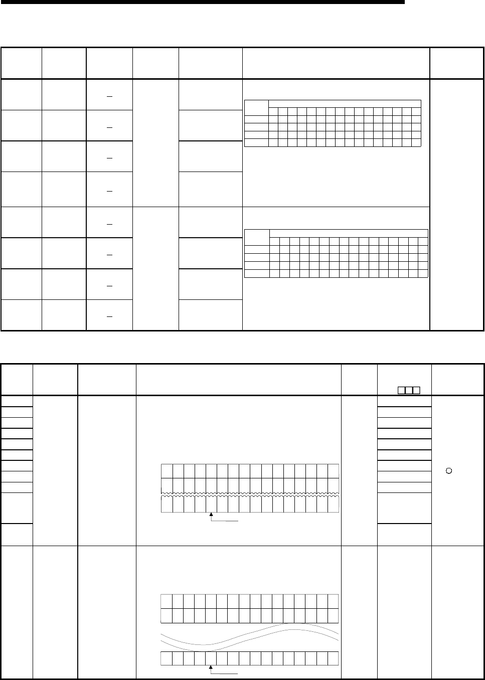
11 - 97 11 - 97
MELSEC-Q
11 TROUBLESHOOTING
Special Register List (Continue)
ACPU
Special
Conversion
Special
Register after
Conversion
Special
Register for
Modification
Name Meaning Details Corresponding
CPU
D9248 SD1248
Stores conditions
for up to numbers 1
to 16
D9249 SD1249
Stores conditions
for up to numbers
17 to 32
D9250 SD1250
Stores conditions
for up to numbers
33 to 48
D9251 SD1251
Local station
operation
status
Stores conditions
for up to numbers
49 to 64
Stores the local station number which is in STOP or PAUSE
mode.
SD1248
SD1249
SD1250
SD1251
b15 b14 b13 b12 b11 b10 b9 b8 b7 b6 b5 b4 b3 b2 b1 b0
L16 L15 L14 L13 L12 L11
L32 L31 L30 L29 L28 L27
L48 L47 L46 L45 L44 L43
L64 L63 L62 L61 L60 L59
L26
L42
L58
L25
L41
L57
L24
L40
L56
L23
L39
L55
L22
L38
L54
L21
L37
L53
L20
L36
L52
L19
L35
L51
L18
L34
L50
L17
L33
L49
L10 L9 L8 L7 L6 L5 L4 L3 L2 L1
Bit
Device
number
The bit corresponding to the station number which is in
STOP or PAUSE mode, becomes "1".
Example: When local stations 7 and 15 are in STOP mode,
bits 6 and 14 of SD1248 become "1", and when
SD1248 is monitored, its value is "16448
(4040H)".
D9252 SD1252
Stores conditions
for up to numbers 1
to 16
D9253 SD1253
Stores conditions
for up to numbers
17 to 32
D9254 SD1254
Stores conditions
for up to numbers
33 to 48
D9255 SD1255
Local station
error
conditions
Stores conditions
for up to numbers
49 to 64
Stores the local station number other than the host, which is
in error.
SD1252
SD1253
SD1254
SD1255
b15 b14 b13 b12 b11 b10 b9 b8 b7 b6 b5 b4 b3 b2 b1 b0
L16 L15 L14 L13 L12 L11
L32 L31 L30 L29 L28 L27
L48 L47 L46 L45 L44 L43
L64 L63 L62 L61 L60 L59
L26
L42
L58
L25
L41
L57
L24
L40
L56
L23
L39
L55
L22
L38
L54
L21
L37
L53
L20
L36
L52
L19
L35
L51
L18
L34
L50
L17
L33
L49
L10 L9 L8 L7 L6 L5 L4 L3 L2 L1
Bit
Device
number
The bit corresponding to the station number which is in error,
becomes "1".
Example: When local station 12 is in error, bit 11 of SD1252
becomes "1", and when SD1252 is monitored, its
value is "2048 (800H) ".
QnA
(11) Fuse blown module
Number Name Meaning Explanation
Set by
(When
set)
Corresponding
ACPU
D9
Corresponding
CPU
SD1300 D9100
SD1301 D9101
SD1302 D9102
SD1303 D9103
SD1304 D9104
SD1305 D9105
SD1306 D9106
SD1307 D9107
SD1308 New
SD1309
to
SD1330
New
SD1331
Fuse blown
module
Bit pattern in units
of 16 points,
indicating the
modules whose
fuses have blown
0: No blown fuse
1: Blown fuse
present
• The numbers of output modules whose fuses have blown are
input as a bit pattern (in units of 16 points).
(If the module numbers are set by parameter, the parameter-set
numbers are stored.)
• Also detects blown fuse condition at remote station output
modules
1514131211109876543210
0001
(YC0) 000 00000000
1
(Y80)
SD1300
00
1
(Y1F0) 0 0 00000000
1
(Y1A)
SD1301 00
00 1
(Y1F
B0) 00000000
SD1331 0001
(Y1F
30)
0
Indicates a blown fuse
• Not cleared even if the blown fuse is replaced with a new one.
This flag is cleared by error resetting operation.
S (Error)
New
+Rem
SD1350
to
SD1381
External
power supply
disconnected
module
(For future
expansion)
Bit pattern in units
of 16 points,
indicating the
modules whose
external power
supply has been
disconnected
0: External power
supply
disconnected
1: External power
supply is not
disconnected
The module number (in units of 16 points) whose external power
supply has been disconnected is input as a bit pattern.
(If the module numbers are set by parameter, the parameter-set
numbers are used.)
15 14 13 12 11 10 9 8 7 6 5 4 3 2 1 0
SD1350
SD1351
0001000 000000001
00
10 0 00000000
1
00
SD1381 00 1 0 0000 00000010
Indicates a blown fuse
S (Error) New QCPU
Remote
11 - 98 11 - 98
MELSEC-Q
11 TROUBLESHOOTING
Special Register List (Continue)
(12) I/O module verification
Number Name Meaning Explanation
Set by
(When
set)
Corresponding
ACPU
D9
Corresponding
CPU
SD1400 D9116
SD1401 D9117
SD1402 D9118
SD1403 D9119
SD1404 D9120
SD1405 D9121
SD1406 D9122
SD1407 D9123
SD1408 New
SD1409
to
SD1430
New to New
SD1431
I/O module
verification
error
Bit pattern, in
units of 16 points,
indicating the
modules with
verification errors.
0: No I/O
verification
errors
1: I/O verification
error present
• When the power is turned on, the module numbers of the I/O
modules whose information differs from the registered I/O module
information are set in this register (in units of 16 points).
(If the I/O numbers are set by parameter, the parameter-set
numbers are stored.)
• Also detects I/O module information
15 14 13 12 11 10 9 8 7 6 543210
000 000 0000000
D9116
00 0 00000000D9117 0 0
0 0 0000 000D9123 0 000
00
00
00
1
( )
X Y
1FE0
1
( )
1
( )
X Y
190
X Y
0
Indicates an I/O module verification error
• Not cleared even if the blown fuse is replaced with a new one.
This flag is cleared by error resetting operation.
S (Error)
New
+Rem
(13) For redundant systems (Host system CPU information 1) for Q4AR only
SD1510 to SD1599 are only valid for redundant systems.
They are all set to 0 for standalone systems.
Number Name Meaning Explanation Set by
(When set)
Corresponding
ACPU
D9
Corresponding
CPU
SD1500
SD1501 Basic period Basic period
tome
• Set the basic period (1 second units) use for the process
control instruction using floating point data.
SD1501 SD1500Floating points data =
U New
SD1502
Process control
instruction detail
error code
Process control
instruction detail
error code
• Shows the detailed error contents for the error that occurred
in the process control instruction
S (Error
occurrence) New
SD1503
Process control
instruction
generated error
location
Process control
instruction
generated error
location
• Shows the error process block that occurred in the process
control instruction.
S (Error
occurrence) New
SD1512
Operation mode
during CPU start
up
Hot start switch
power out time
• Shows the power out time (S) during the automatic switch
from hot start to initial start in the operation mode when the
CPU module is started up.
S (Initial) New
SD1590 Switch request
network No.
Request origin
network No.
• Stores the request origin at work No. when the SM1590 is
turned on.
S (Error
occurrence) New
Q4AR
1 Host system CPU information is stored.
11 - 99 11 - 99
MELSEC-Q
11 TROUBLESHOOTING
Special Register List (Continue)
(14) For redundant systems (Other system CPU information 1) for Q4AR only
SD1600 to SD1659 is only valid during the back up mode for redundant systems, and refresh
cannot be done when in the separate mode. When a standalone system SD1600 to SD1699
are all 0.
Number Name Meaning Explanation Set by
(When set)
Corresponding
ACPU
SD 2
Corresponding
CPU
SD1600 Diagnosis error
Diagnosis error
code.
• Stores as BIN code the error code of the error that occurred
during the other system CPU diagnosis.
• Stores the latest error currently occurring.
S (Each
END) New
SD1601
SD1602
SD1603
Diagnosis error
occurrence
time
Diagnosis error
occurrence time
• SD1600 stores the updated date and time.
• Stores each of the BCD two digits.
• Refer to SD1 to SD3 for the storage status.
(SD1 SD1601, SD2 SD1602, SD3 SD1603)
S (Each
END) New
SD1604
Error
information
classification
Error
information
classification
• Stores the error comment information/individual information
classification code.
• Refer to SD4 for the storage status.
S (Each
END) New
SD1605
SD1606
SD1607
SD1608
SD1609
SD1610
SD1611
SD1612
SD1613
SD1614
SD1615
Error common
information
Error common
information
• Stores the common information for the error code.
• Refer to SD5 to SD15 for the storage status.
(SD5 SD1605, SD6 SD1606, SD7 SD1607,
SD8 SD1608, SD9 SD1609, SD10 SD1610,
SD11 SD1611, SD12 SD1612, SD13 SD1613,
SD14 SD1614, SD15 SD1615)
S (Each
END) New
SD1616
SD1617
SD1618
SD1619
SD1620
SD1621
SD1622
SD1623
SD1624
SD1625
SD1626
Error individual
information
Error individual
information
• Stores the individual information for the error code Refer to
SD16 to SD26 for the storage status.
(SD16 SD1616, SD17 SD1617, SD18 SD1618,
SD19 SD1619, SD20 SD1620, SD21 SD1621,
SD22 SD1622, SD23 SD1623, SD24 SD1624,
SD25 SD1625, SD26 SD1626)
S (Each
END) New
SD1650 Switch status CPU switch
status
• Stores the CPU module switch status.
• Refer to SD200 for the storage status. (SD1650 SD200)
S (Each
END) New
SD1651 LED status CPU-LED status
• Stores the CPU module's LED status.
• Shows 0 when turned off, 1 when turned on, and 2 when
flicking.
• Refer to SD201 for the storage status. (SD1651 SD201)
S (Each
END) New
SD1653 CPU operation
status
CPU operation
status
• Stores the CPU module operation status. Refer to SD203 for
the storage status. (SD1653 SD203)
S (Each
END) New
Q4AR
1 Stores other system CPU self-diagnosis information and system information.
2 Shows the special register (SD ) for the host system CPU.
(15) For redundant systems (Trucking) for Q4AR only
SD1700 to SD1799 is valid only for redundant systems. These are all 0 for standalone
systems.
Number Name Meaning Explanation Set by
(When set)
Corresponding
ACPU
SD 2
Corresponding
CPU
SD1700 Trucking error
detection count
Trucking error
detection count • Make it the trucking error detection +1. S (Error
occurrence) New Q4AR
2 Shows the special register (SD ) for the host system CPU.
App - 1 App - 1
MELSEC-Q
APPENDICES
APPENDICES
APPENDIX 1 Error Code Return to Origin During General Data Processing
The CPU module returns an error code to the general data processing request origin
when an error occurs and there is a general data processing request form the
peripheral equipment, intelligent function module, or network system. If an error occurs
when a general data processing is requested from the peripheral devices, intelligent
function module, and network system.
POINT
This error code is not an error that is detected by the CPU module self-diagnosis
function, so it is not stored in the special relay (SD0).
When the request origin is a GX Developer, a message or an error code is
displayed.
When the request origin is an intelligent function module or network system, an
error is returned to the process that was requested.
APPENDIX 1.1 Error code overall explanation
These error codes differs depending on the error No. of the location the error was
detected. The following table shows the relationship between the error detection
location and the error code.
Error detection location Error Code
(hexadecimal) Error description reference destination
CPU module 4000H to 4FFFH Refer to Appendix 1.2.
Intelligent function
module 7000H to 7FFFH User's manuals of intelligent function module
Network system F000H to FFFFH Q Corresponding MELSECNET/H Network System
Reference Manual
App
App - 2 App - 2
MELSEC-Q
APPENDICES
APPENDIX 1.2 Description of the errors of the error codes (4000H to 4FFFH)
The error contents of the error codes (4000H to 4FFFH) detected by the CPU module
and the messages displayed by the GX Developer are shown below.
Error code
(hexadecimal)
Error
item Error description Countermeasure
4000H Sum check error Check the connection status of the connection cable
with the CPU module
4001H Remote request that is not handled was
executed. Check the requested remote operation.
4002H
4003H
Command for which a global request cannot be
performed was executed. Check the requested command.
4004H CPU module cannot execute the request
contents because it is in system protect Turn off the CPU module system protect switch.
4005H The volume of data handled according to the
specified request is too large.
Reduce the volume of data to that which can be
processed at the specified request.
4006H The password cannot be deleted. Delete the set password.
4008H
CPU
related
error
The CPU module is not BUSY (The buffer is not
vacant). After the free time has passed, reexecute the request.
4010H The CPU module is running to the request
contents cannot be executed. Execute after setting the CPU module to STOP status.
4011H
CPU mode
error The CPU module is not in the STEP-RUN
status so the request contents cannot be
executed.
Execute after setting the CPU module to STEP-RUN
status.
App

App - 3 App - 3
MELSEC-Q
APPENDICES
Error code
(hexadecimal)
Error
item Error description Countermeasure
4021H The specified drive memory does not exist or
there is an error. Check the specified drive memory status.
4022H The file with the specified file name or file No.
does not exist. Check the specified file name and file No.
4023H The file name and file No. of the specified file do
not match. Delete the file and then recreate the file.
4024H The specified file cannot be handled by a user. Do not access the specified file.
4025H The specified file is processing the request from
a different location.
Forcefully execute the request forcibly.
Or reexecute the request after the processing from the
other location has ended.
4026H The keyword specification set in the
corresponding drive memory is required.
Access by specifying the keyword set in the
corresponding drive memory.
4027H The specified range exceeds the file range. Check the specified range and access within that range.
4028H The same file already exists. Forcefully execute the request forcibly.
Or reexecute after changing the file name.
4029H The specified file capacity cannot be obtained.
Revise the specified file contents.
Or reexecute after cleaning up and reorganizing the
specified drive memory.
402BH The request contents cannot be executed in the
specified drive memory.
Do not execute a request for a specified drive memory in
which an error has occurred.
402CH
CPU file
related error
Currently the request contents cannot be
executed. Reexecute after the free wait time has passed.
4030H The specified device name cannot be handled. Check the specified device name.
4031H The specified device No. is outside the range. Check the specified device No.
4032H There is a mistake in the specified device
qualification. Check the specified device qualification method.
4033H
CPU device
specified error
Writing cannot be done because the specified
device is for system use.
Do not write the data in the specified device, and do not
turn on or off.
4040H The request contents cannot be executed in the
specified intelligent function module.
Do not conduct a request for a specified intelligent
function module in which an error has occurred.
4041H
The access range exceeds the buffer memory
range of the specified intelligent function
module.
Check the header address and access number of points
and access using a range that exists in the intelligent
function module.
4042H The specified intelligent function module cannot
be accessed.
Check that the specified intelligent function module is
operating normally.
4043H The intelligent function module does not exist in
the specified position.
Check the header I/O No. of the specified intelligent
function module.
4044H A control bus error has occurred. Check that there is no error in the intelligent function
module or in the hardware of another module.
4045H The setting required to conduct simulation has
not been made. Conduct a simulation setting.
4046H
Intelligent
function
module
specification
error
The device header or number of points in the
simulation is not in 16point unit.
Check the device header No. or number of points and
correct them to 16 point units.
App - 4 App - 4
MELSEC-Q
APPENDICES
Error code
(hexadecimal) Error
item Error description Countermeasure
4050H
The request contents cannot be executed
because the memory card write protect switch
is on.
Turn off the memory card write protect switch.
4051H The specified device memory cannot be
accessed.
Check the following and make it countermeasures.
• Is the memory one that can be used?
• Is the specified drive memory correctly installed?
4052H The specified file attribute is read only so the
data cannot be written.
Do not write data in the specified file.
Or change the file attribute.
4053H An error occurred when writing data to the
specified drive memory.
Check the specified drive memory.
Or reexecute write after changing the corresponding
drive memory.
4054H
Protect error
An error occurred when deleting the data in the
specified drive memory.
Check the specified drive memory.
Or re-erase after replacing the corresponding drive
memory.
4060H
The monitor condition registration CPU module
system area is already being used by another
piece of equipment.
Reexecute monitor after the monitor by the other
equipment has completed. Or increase the system area
of the program memory using the format with option.
4061H Communication failed. Execute a re-communication.
4062H
The monitor detail condition is already being
used and monitored by another piece of
equipment.
Do not conduct monitor detail condi-tions from the
specified equipment.
Or reexecute monitoring after deleting the monitor detail
conditions of the other equipment.
4063H The number of the file lock registrations
exceeds 16. Reduce the number of registrations to 16 or less.
4064H There is a problem with the specified contents. Check the specified contents.
4065H The device allocation information differs from
the parameter.
Check the parameter.
Or check the data.
4066H A keyword that differs from the keyword set in
the specified driver memory has been specified. Check the specified keyword.
4067H The specified monitor file cannot be obtained. Conduct monitor after obtaining the monitor file.
4068H
Registration/deletion cannot be conducted
because the specified command is being
executed.
Reexecute the command after the request from the
other equipment has been completed.
4069H The conditions have already been reached by
the device match.
Check the monitor conditions.
Or reconduct monitor registration and execute monitor.
406AH
Online
registration
error
A drive other than Nos. 1 to 3 has been
specified. Check the specified drive and specify the correct drive.
4070H Circuit inquiry
Program before correction and the registration
program differ.
Check the registration program and make the programs
match.
4080H Data error Check the requested data contents.
4081H The sort subject cannot be detected. Check the data to be searched.
4082H The specified command is executing and
therefore cannot be executed.
Reexecute the command after the request from the
other equipment is completed.
4083H
Other errors
Trying to execute a program that is not
registered in the parameter. Register the program to be executed in the parameter.
App - 5 App - 5
MELSEC-Q
APPENDICES
Error code
(hexadecimal) Error
item Error description Countermeasure
4084H The specified pointer P, I cannot be detected. Check the data to be searched.
4085H Pointer P, I cannot be specified because the
program is not specified in the parameter.
Specify pointer P, I after registering the program to be
executed in the parameter.
4086H Pointer P, I has already been added. Check the pointer No. to be added and make correction.
4087H Trying to specify too many pointers. Check the specified pointer and make a correction.
4088H The specified step No. was not in the instruction
header. Check the specified step No. and make a correction.
4089H An END instruction was inserted/deleted while
the CPU module was running.
Conduct Insert/removal after the CPU module has
stopped.
408AH The file capacity was exceeded by the write
during Run. Write the program after the CPU module has stopped.
408BH
Other errors
The remote request cannot be executed. Reexecute after the CPU module is in a status where
the mode request can be executed.
4090H The block breakpoint number was exceeded. Check the number of settings and make a correction.
4091H There is a mistake in the block breakpoint
registration number.
Check the number of registrations and make a
correction.
4092H The step breakpoint number has been
exceeded.
Check the number of registrations and make a
correction.
4093H There is a mistake in the step breakpoint
registration number.
Check the number of registrations and make a
correction.
4094H Tried to execute a request during block
continuous processing. Reconduct the request after the processing has ended.
4095H Tried to execute a request during block forced
execution processing. Reconduct the request after the processing has ended.
4096H Tried to execute a request during step
continuous processing. Reconduct the request after the processing has ended.
4097H Tried to execute a request during step forced
execution processing. Reconduct the request after the processing has ended.
4098H Tried to execute a request during one step
continuous processing. Reconduct the request after the processing has ended.
4099H Tried to execute a request during one step
forced execution processing. Reconduct the request after the processing has ended.
409AH Tried to execute a request during block forced
end processing. Reconduct the request after the processing has ended.
409BH Tried to execute a request during step forced
end processing. Reconduct the request after the processing has ended.
409CH Tried to execute a request during hold step
reset processing. Reconduct the request after the processing has ended.
409DH A block No. that has not been created or that
exceeds the range has been specified. Check the setting contents and make a correction.
409EH A step No. that was not created was specified. Check the setting contents and make a correction.
409FH
Online
registration
errors during
SFC STEP-
RUN
The specified number of cycles is outside the
range.
Check the number of registrations and make a
correction.
App - 6 App - 6
MELSEC-Q
APPENDICES
Error code
(hexadecimal) Error
item Error description Countermeasure
40A0H A block No. outside the range was specified. Check the setting contents and make a correction.
40A1H A number of blocks that exceeds the range was
specified. Check the number of settings and make a correction.
40A2H A step No. that is outside the range was
specified. Check the setting contents and make a correction.
40A3H A number of steps that exceeds the range was
specified. Check the number of settings and make a correction.
40A4H A sequence step No. outside the range was
specified. Check the setting contents and make a correction.
40A5H The specified device was outside the range. Check the number of settings and make a correction.
40A6H
SFC device
specification
error
There is a mistake in the block specification
pattern or the step specification pattern. Check the setting contents and make a correction.
40B0H The wrong drive was specified. Check the setting contents and make a correction.
40B1H The specified program does not exist. Check the specified file name and make a correction.
40B2H The specified program was not an SFC
program. Check the specified file name and make a correction.
40B3H
SFC file related
error
There was an SFC dedicated instruction in the
write during run area. Check the setting contents and make a correction.
41D0H The route directory has no free space.
Increase the free space of the specified drive.
Optimize the specified drive to increase continuous free
areas.
41D1H The file pointer is insufficient. Specify the correct file pointer.
41D5H The file of the same name exists. Change the file name.
41DFH The disk is write-protected. Cancel the write protection of the disk and execute
again.
41E0H The drive does not respond. Check for the specified drive. If it exists, check its status.
41E1H The address or sector is not found. Check if the target is a ROM drive or not.
41E4H The file cannot be accessed properly. Execute again after resetting the CPU module.
41E8H The drive format information is illegal. Format the target drive.
41E9H At the time of file access, time-out occurred
during waiting for access. Execute again after some time.
41EBH The path name is too long. Check the length of the path name.
41ECH The disk is logically broken. Change the specified drive.
41EDH
An attempt to make a file continuous failed.
(There are enough free file areas, which cannot
be taken continuously.)
Optimize the specified drive to increase continuous free
areas.
41F2H The specified drive is ROM. Check the specified drive. (Format it for RAM.)
41FBH The same starting source has already opened
the specified file. Check if it is being processed by another application.
41FCH An attempt was made to erase the mounted
drive. Execute again after dismounting the drive.
41FDH The Flash ROM is not formatted. Erase the specified drive.
41FEH The memory card is not inserted. Insert or reinsert the memory card.
41FFH
File-related
errors
The memory card type differs. Check the memory card type.
4A00H
(1) The specified station could not be accessed
because a routing parameter was not set in
the related station.
(2) Though routing via the multiple CPU system
is attempted, the control CPU of the network
module that relays the data is not active.
(1) Set the routing parameter for accessing the specified
station in the related station.
(2) Try after a while. Or check if the system relaying the
data is active, then start communication.
4A01H The network with the No. set in the routing
parameter does not exist. Check the routing parameter set in the related station
and make a correction.
4A02H
Link related
error
Cannot access the specified station. Check if an error has occurred in the network module
and if the module is offline.
4B00H Object related
error An error occurred in the access destination or in
a relay station.
Check if an error has occurred in the specified access
destination or in a relay station to the access station and
if so take countermeasures.
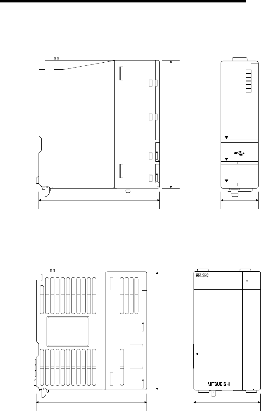
App - 7 App - 7
MELSEC-Q
APPENDICES
APPENDIX 2 External Dimensions
APPENDIX 2.1 CPU module
89.3(3.52)
98(3.86)
Q02HCPU
RS-232
USB
MODE
RUN
ERR.
USER
BAT.
BOOT
27.4(1.08)
PULL
Unit: mm (inch)
APPENDIX 2.2 Power supply module
(1) Power Supply Module (Q61P-A1, Q61P-A2, Q62P, Q63P)
Q61P-A1 POWER
PULL
90(3.54) 55.2(2.17)
98(3.86)
Unit: mm (inch)
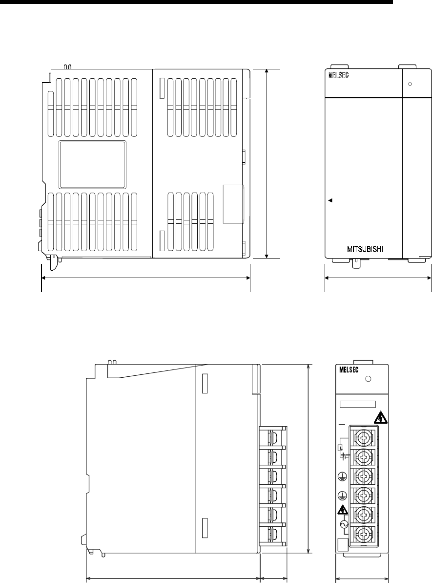
App - 8 App - 8
MELSEC-Q
APPENDICES
(2) Power Supply Module (Q64P)
Q64P POWER
PULL
115 (4.53) 55.2 (2.17)
98 (3.86)
Unit: mm (inch)
(3) Power Supply Module (Q61SP)
Q61SP
100-
240V
AC
Q61SP
POWER
INPUT
50/60Hz 40VA
100-240VAC
ERR.
24VDC
0.5A
INPUT
OUTPUT 5VDC 2A
MITSUBISHI
27.4 (1.08)
14
(0.55)
90 (3.54)
98 (3.86)
(FG)
(LG)
Unit: mm (inch)
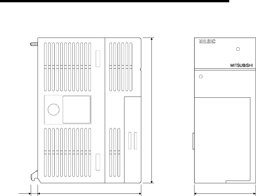
App - 9 App - 9
MELSEC-Q
APPENDICES
(4) Power Supply Module (A1S61PN, A1S62PN, A1S63P)
A1S61PN
POWER
INPUT
100-240VAC
105VA
50 / 60Hz
OUTPUT
DC 5V 5A
NP
6.5 93.6(3.69) 54.5(2.15)
130(5.12)
(0.26)
Unit: mm (inch)
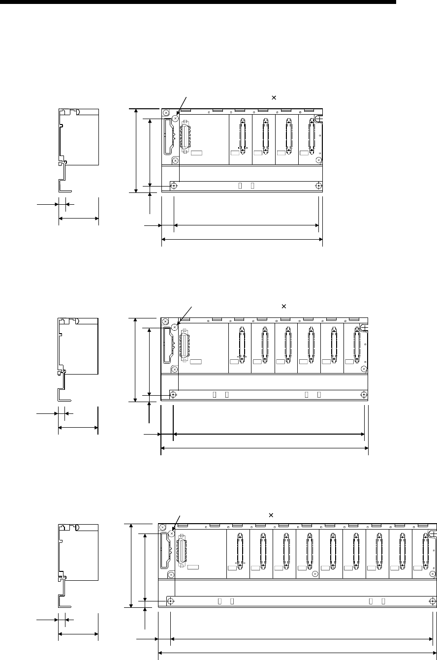
App - 10 App - 10
MELSEC-Q
APPENDICES
APPENDIX 2.3 Main base unit
(1) Main Base Unit (Q33B)
I/O0
CPU
POWER I/O2I/O1
5V
56
F6
15.5 169±0.3(6.65±0.01)
189(7.44)
(0.61)
98(3.86)
80±0.3
(3.15±0.01)
7
(0.28)
7.5
44.1
(1.74)
(0.30)
4-mounting screws (M4 14)
Unit: mm (inch)
(2) Main Base Unit (Q35B)
I/O0
CPU
POWER I/O2I/O1 I/O3 I/O4
5V
56
F6
15.5 224.5±0.3(8.85±0.01)
245(9.65)
(0.61)
98(3.86)
80±0.3
(3.15±0.01)
7
(0.28)
7.5
44.1
(1.74)
(0.30)
4-mountiong screws (M4 14)
Unit: mm (inch)
(3) Main Base Unit (Q38B)
98(3.86)
80±0.3
(3.15±0.01)
7
(0.28)
7.5
44.1
(1.74)
(0.30)
I/O1I/O0
CPU I/O5I/O4I/O3I/O2 I/O6 I/O7
15.5 308±0.3(12.14±0.01)
328(12.92)
POWER
5V
56
F6
(0.61)
4-mountiong screws (M4 14)
Unit: mm (inch)
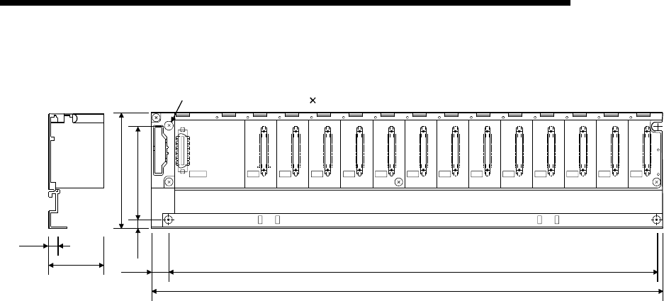
App - 11 App - 11
MELSEC-Q
APPENDICES
(4) Main Base Unit (Q312B)
15.5
439(17.30)
419±0.3(16.51±0.01)
I/11I/10I/09I/08I/07I/06I/05I/04I/03I/02I/01I/00
CPU
POWER
5V
56
F6
98(3.86)
80±0.3
(3.15±0.01)
7
(0.28)
7.5
44.1
(1.74)
(0.30)
(0.61)
4-mountiong screws (M4 14)
Unit: mm (inch)
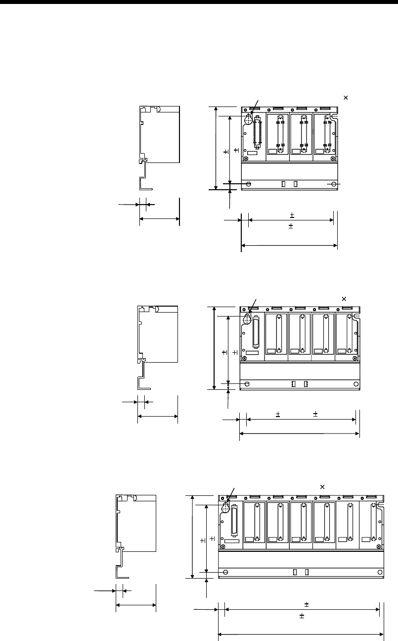
App - 12 App - 12
MELSEC-Q
APPENDICES
APPENDIX 2.4 Slim type main base unit
(1) Main Base Unit (Q32SB)
SG
5V
I/O0 I/O1CPU
POWER
98 (3.86)
780 0.3
7.5
44.1
114 (4.49)
8.5 101 0.3
(3.98 0.01)
4-mounting screws (M4 12)
(3.15 0.01)
(0.28)
(0.33)
(1.74)
(0.30)
Unit: mm (inch)
(2) Main Base Unit (Q33SB)
7.5
44.1
142 (5.59)
98 (3.86)
780 0.3
8.5 129 0.3 (5.08 0.01)
SG
5V
I/O2I/O0 I/O1
CPU
POWER
4-mounting screws (M4 12)
(0.28) (3.15 0.01)
(0.30)
(1.74) (0.33)
Unit: mm (inch)
(3) Main Base Unit (Q35SB)
7.5
44.1
197.5 (7.78)
80 0.3
8.5 184.5 0.3
SG
5V
I/O3
I/O2 I/O4
I/O0 I/O1
CPU
POWER
4-mounting screws (M4 12)
98 (3.86)
(3.15 0.01)
(0.33)
7
(0.28)
(7.26 0.01)
(1.74)
(0.30)
Unit: mm (inch)
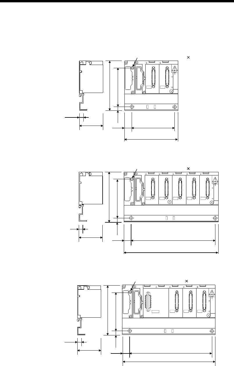
App - 13 App - 13
MELSEC-Q
APPENDICES
APPENDIX 2.5 Extension base unit
(1) Extension Base Unit (Q52B)
7.5
(0.30) 44.1
(1.74)
98 (3.86)
80±0.3
(3.15±0.01)
(0.28)
15.5
(0.61) 106 (4.17)
83.5±0.3
(3.29±0.01)
I/O0 I/O1
OUTIN
4-mounting screws (M4 14)
7
Unit: mm (inch)
(2) Extension Base Unit (Q55B)
I/O2I/O1I/O0 I/O3 I/O4
7.5
(0.30) 44.1
(1.74)
98 (3.86)
80±0.3
(3.15±0.01)
7
15.5
189 (7.44)
167±0.3
(6.57±0.01)
OUTIN
4-mounting screws (M4 14)
(0.28)
(0.61)
Unit: mm (inch)
(3) Extension Base Unit (Q63B)
I/O0
F6
I/O2I/O1
15.5
189(7.44)
167±0.3(6.57±0.01)
POWER
5V
56
OUTIN
(0.30) 44.1
(1.74)
7.5
98(3.86)
80±0.3
(3.15±0.11)
7
(0.28)
(0.61)
4-mounting screws (M4 14)
Unit: mm (inch)
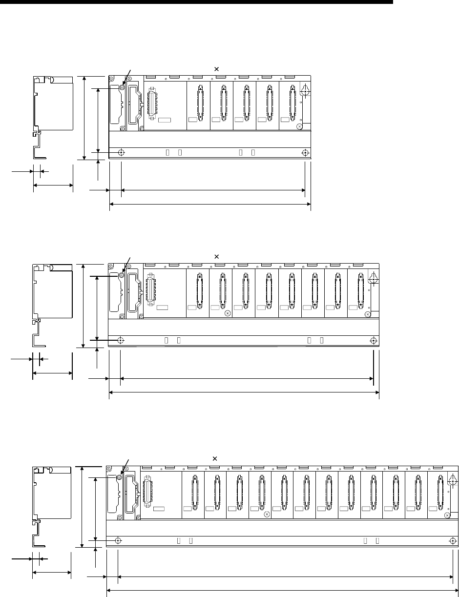
App - 14 App - 14
MELSEC-Q
APPENDICES
(4) Extension Base Unit (Q65B)
I/O0
F6
I/O2I/O1 I/O3 I/O4
15.5
245(9.65)
222.5±0.3(8.77±0.01)
POWER
5V
56
OUTIN
(0.30) 44.1
(1.74)
7.5
98(3.86)
80±0.3
(3.15±0.01)
7
(0.28)
(0.61)
4-mounting screws (M4 14)
Unit: mm (inch)
(5) Extension Base Unit (Q68B)
98(3.86)
80±0.3
(3.15±0.01)
7
(0.28)
(0.30) 44.1
(1.74)
7.5
I/O2I/O1I/O0
POWER
F6
I/O5I/O4I/O3 I/O6 I/O7
15.5
328(12.92)
306±0.3(12.06±0.01)
5V
56
OUTIN
(0.61)
4-mounting screws (M4 14)
Unit: mm (inch)
(6) Extension Base Unit (Q612B)
98(3.86)
80±0.3
(3.15±0.01)
7
(0.28)
(0.30) 44.1
(1.74)
7.5
I/O11I/O10I/O9I/O8I/O7I/O6I/O5I/O4I/O3I/O2I/O1I/O0
15.5
439(17.30)
417±0.3(16.43±0.01)
POWER
F6
5V
56
OUTIN
(0.61)
4-mounting screws (M4 14)
Unit: mm (inch)
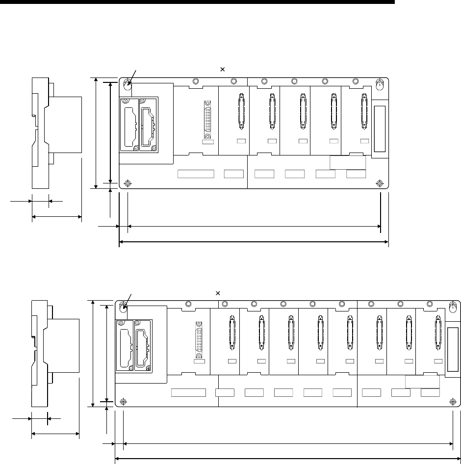
App - 15 App - 15
MELSEC-Q
APPENDICES
(7) Extension Base Unit (QA1S65B)
130 (5.12)
110 (4.33)
315(12.41)
295±0.3(11.62±0.01)
IN OUT
10(0.39)
POWER
5V
SG
FG
I/O0 I/O1 I/O2 I/O3 I/O4
QA1S65B
51.2
16.4
(2.02)
(0.65)
10
(0.39)
4-mounting screws (M5 25)
Unit: mm (inch)
(8) Extension Base Unit (QA1S68B)
I/O0 I/O7I/O6I/O5I/O4I/O3I/O2I/O1
QA1S68B
130(5.12)
110(4.33)
10(0.39)
10
420(16.55)
400±0.3(15.76±0.01)
IN OUT
POWER
5V
SG
FG
16.4
51.2
(0.65)
(2.02)
(0.39)
4-mounting screws (M5 25)
Unit: mm (inch)
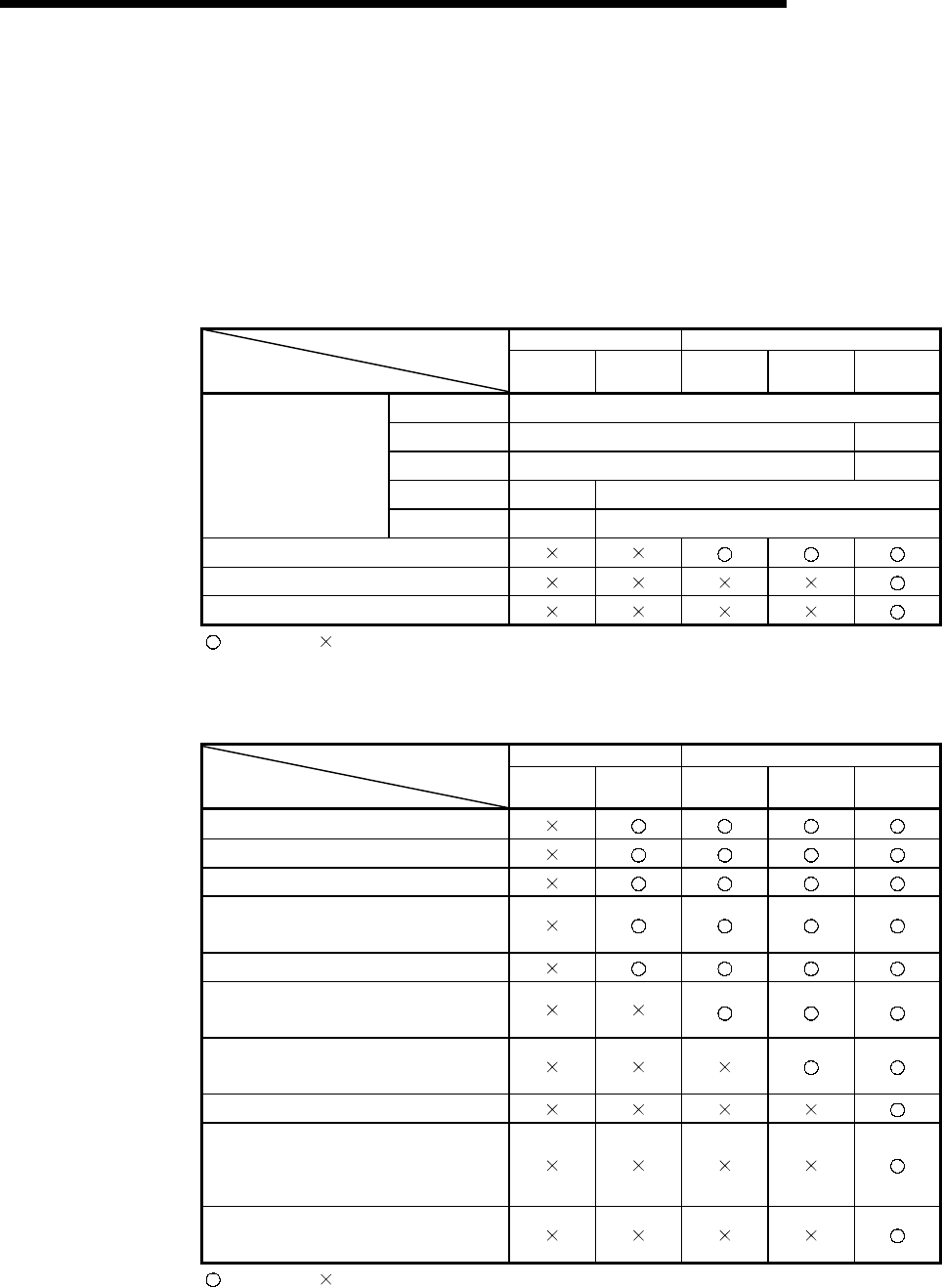
App - 16 App - 16
MELSEC-Q
APPENDICES
APPENDIX 3 Upgraded Functions of High Performance Model QCPU
The High Performance model QCPU is upgraded to add functions and change the
specifications.
The functions and specifications that can be used by the High Performance model
QCPU change depending on the function version/serial number.
APPENDIX 3.1 Specification comparison
Serial No. of CPU Module Function Version A Function Version B
Specifications 02091
or earlier 02092
or later —— 03051
or later 04012
or later
Q02CPU 32kbyte
Q02HCPU 32kbyte 64kbyte
Q06HCPU 32kbyte 64kbyte
Q12HCPU 32kbyte 256kbyte
Standard RAM capacity
Q25HCPU 32kbyte 256kbyte
CPU shared memory
Extended life battery SRAM card
Compatibility with 2Mbyte SRAM card
: Available, : N/A
APPENDIX 3.2 Function comparison
Serial No. of CPU Module Function Version A Function Version B
Added Function 02091
or earlier 02092
or later —— 03051
or later 04012
or later
Automatic write to standard ROM
Enforced ON/OFF for external I/O
Remote password setting
Compatibility with MELSECNET/H
remote I/O network
Interrupt module (QI60) compatibility
Compatibility with the multiple CPU
system
Installation of PC CPU module into the
multiple CPU system
High speed interrupt
Compatibility with index modification for
module designation of dedicated
instruction
Selection of refresh item for COM
instruction
: Available, : N/A
For function details, refer to the High Performance model QCPU (Q mode) User's
Manual (Function Explanation, Program Fundamentals).
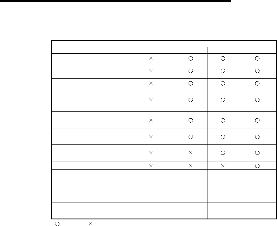
App - 17 App - 17
MELSEC-Q
APPENDICES
APPENDIX 3.3 Added functions and the corresponding GX Developer versions
GX Developer
Added Function SW4D5C-GPPW-E
SW5D5C-GPPW-E Version 6 Version 7 Version 7.10L
Automatic write to standard ROM
External I/O can be turned
ON/OFF forcibly
Remote password setting
Compatibility with
MELSECNET/H remote I/O
network
Interrupt module (QI60)
compatibility
Compatibility with the multiple
CPU system
Installation of PC CPU module
into the multiple CPU system
High speed interrupt
Compatibility with index
modification for module
designation of dedicated
instruction
— — — —
Selection of refresh item for COM
instruction — — — —
: Available, : N/A,
— : Function not related to GX Developer

Index - 1 Index - 1
INDEX
[A]
Allowable momentary power failure period ... 4- 3
AnS Series.....................................................A-12
[B]
Base unit
Extension ....................................2- 3, 6- 5, 6- 6
External dimensions diagram
.....App- 9 to App-13
Installation and removal
of the module................................9-14 to 9-17
Installation dimensions.............................. 9-12
Installation direction................................... 9-13
Installation position.................................... 9-12
Names of parts ........................................... 6- 3
Specifications.............................................. 6- 1
Battery
Installation................................................... 7- 6
Replacement procedure
(CPU module)........................................... 10- 6
Replacement procedure
(SRAM card)............................................. 10- 7
Replacement standard ............................. 10- 5
Boot operation ......................................4- 7,11-13
[C]
Circuit
Fail-safe ...................................................... 9- 5
System design ..................................... 9- 3,9- 4
Clock function................................................. 4- 3
Constant scan ................................................ 4- 1
Control method............................................... 4- 1
CPU
Installation and removal ............................ 9-14
Performance ............................................... 4- 1
[D]
DIN rail
~ installation adapter ................................. 9-11
Applicable .................................................. 9-11
Intervals of ~ installation screws ............... 9-11
[E]
Extension
Base unit..................................................... 6- 2
Cable ................................................. 6- 3, 9-19
Stage ....................................................2- 4,6- 7
External dimensions
CPU module...................................App- 7, 4- 3
Base unit.........................................App- 9, 6- 1
Power supply module.....................App- 7, 5- 1
[G]
GX Developer ............................................... A-12
[H]
High Performance model QCPU...........A-12,1- 1
[I]
I/O control mode .............................................4- 1
Installation and removal..................................9- 9
Intelligent function module
Direct device................................................4- 3
Limit .............................................................2- 6
Internal current consumption..........................4- 3
[L]
Latch range .....................................................4- 3
LED
"BAT." ~ is turned on.................................11- 8
"BOOT." ~ is flickering. .............................11- 9
"ERR." ~ is turned on/flickering. ...............11- 7
"MODE" ~ is not turned on. ......................11- 3
"MODE" ~ is flickering...............................11- 4
"POWER" ~ is turned off...........................11- 5
"RUN" ~ is turned off/flickering. ................11- 6
"USER" ~ is turned on. .............................11- 8
Names .........................................................4- 4
Limit.................................................................2- 6
Link direct device ............................................4- 3
[M]
Maximum number of extension stages ..........2- 4
Memory
Capacity.......................................................4- 1
Card.............................................................7- 1
[N]
Number of device I/O points...........................4- 1
Number of occupied I/O points.......................4- 1
Ind

Index - 2 Index - 2
[P]
Performance................................................... 4- 1
Power supply module
External dimensions diagram.................App- 7
Example of wiring ...................................... 9-25
Installation.................................................. 9-14
Names of parts and settings ...................... 5- 8
Specifications.............................................. 5- 1
Wiring......................................................... 9-22
Processing speed........................................... 4- 1
Programming language.................................. 4- 1
[Q]
QA1S65B, QA1S68B
External dimensions...............................App- 9
Names of parts ........................................... 6- 6
Specifications.............................................. 6- 2
QC05B, QC06B, QC12B, QC30B, QC50B,
QC100B ......................................................... 6- 3
Q32SB, Q33SB, Q35SB
External dimensions..............................App-11
Names of parts ........................................... 6- 5
Specifications.............................................. 6- 1
Q33B, Q35B, Q38B, Q312B
External dimensions................................App-9
Names of parts ........................................... 6- 4
Specifications.............................................. 6- 1
Q Series.........................................................A-19
[R]
Remote RUN/PAUSE contact ....................... 4- 3
[S]
Specifications
Base unit..................................................... 6- 1
Battery......................................................... 7- 2
CPU............................................................. 4- 1
Extension cable .......................................... 6- 2
General ....................................................... 3- 1
Memory card............................................... 7- 1
Power supply module................................. 5- 1
System configuration
Configured equipment................................ 2- 1
Outline......................................................... 2- 4
Peripheral device........................................ 2- 3
[T]
Tightening torque of screw .............................9- 9
Total number of instructions ...........................4- 1
[W]
Weight
Base unit......................................................6- 1
Battery .........................................................7- 2
CPU .............................................................4- 3
Extension cable...........................................6- 3
Memory card ...............................................7- 1
Power supply module..................................5- 2
Wiring
Extension cable...........................................2- 3
Heat generation...........................................9- 6
I/O module..................................................9-24
Power supply module........................ 9-22,9-25
Wiring of the I/O module ............................9-24
Ind

WARRANTY
Please confirm the following product warranty details before starting use.
1. Gratis Warranty Term and Gratis Warranty Range
If any faults or defects (hereinafter "Failure") found to be the responsibility of Mitsubishi occurs during use of the product
within the gratis warranty term, the product shall be repaired at no cost via the dealer or Mitsubishi Service Company.
Note that if repairs are required at a site overseas, on a detached island or remote place, expenses to dispatch an
engineer shall be charged for.
[Gratis Warranty Term]
The gratis warranty term of the product shall be for one year after the date of purchase or delivery to a designated
place.
Note that after manufacture and shipment from Mitsubishi, the maximum distribution period shall be six (6) months, and
the longest gratis warranty term after manufacturing shall be eighteen (18) months. The gratis warranty term of repair
parts shall not exceed the gratis warranty term before repairs.
[Gratis Warranty Range]
(1) The range shall be limited to normal use within the usage status, usage methods and usage environment, etc.,
which follow the conditions and precautions, etc., given in the instruction manual, user's manual and caution labels
on the product.
(2) Even within the gratis warranty term, repairs shall be charged for in the following cases.
1. Failure occurring from inappropriate storage or handling, carelessness or negligence by the user. Failure caused
by the user's hardware or software design.
2. Failure caused by unapproved modifications, etc., to the product by the user.
3. When the Mitsubishi product is assembled into a user's device, Failure that could have been avoided if functions
or structures, judged as necessary in the legal safety measures the user's device is subject to or as necessary
by industry standards, had been provided.
4. Failure that could have been avoided if consumable parts (battery, backlight, fuse, etc.) designated in the
instruction manual had been correctly serviced or replaced.
5. Failure caused by external irresistible forces such as fires or abnormal voltages, and Failure caused by force
majeure such as earthquakes, lightning, wind and water damage.
6. Failure caused by reasons unpredictable by scientific technology standards at time of shipment from Mitsubishi.
7. Any other failure found not to be the responsibility of Mitsubishi or the user.
2. Onerous repair term after discontinuation of production
(1) Mitsubishi shall accept onerous product repairs for seven (7) years after production of the product is discontinued.
Discontinuation of production shall be notified with Mitsubishi Technical Bulletins, etc.
(2) Product supply (including repair parts) is not possible after production is discontinued.
3. Overseas service
Overseas, repairs shall be accepted by Mitsubishi's local overseas FA Center. Note that the repair conditions at each FA
Center may differ.
4. Exclusion of chance loss and secondary loss from warranty liability
Regardless of the gratis warranty term, Mitsubishi shall not be liable for compensation to damages caused by any cause
found not to be the responsibility of Mitsubishi, chance losses, lost profits incurred to the user by Failures of Mitsubishi
products, damages and secondary damages caused from special reasons regardless of Mitsubishi's expectations,
compensation for accidents, and compensation for damages to products other than Mitsubishi products and other duties.
5. Changes in product specifications
The specifications given in the catalogs, manuals or technical documents are subject to change without prior notice.
6. Product application
(1) In using the Mitsubishi MELSEC programmable logic controller, the usage conditions shall be that the application will
not lead to a major accident even if any problem or fault should occur in the programmable logic controller device, and
that backup and fail-safe functions are systematically provided outside of the device for any problem or fault.
(2) The Mitsubishi general-purpose programmable logic controller has been designed and manufactured for applications
in general industries, etc. Thus, applications in which the public could be affected such as in nuclear power plants and
other power plants operated by respective power companies, and applications in which a special quality assurance
system is required, such as for Railway companies or National Defense purposes shall be excluded from the
programmable logic controller applications.
Note that even with these applications, if the user approves that the application is to be limited and a special quality is
not required, application shall be possible.
When considering use in aircraft, medical applications, railways, incineration and fuel devices, manned transport
devices, equipment for recreation and amusement, and safety devices, in which human life or assets could be greatly
affected and for which a particularly high reliability is required in terms of safety and control system, please consult
with Mitsubishi and discuss the required specifications.
HEADQUARTERS
MITSUBISHI ELECTRIC EUROPE
EUROPE B.V.
Gothaer Straße 8
D-40880 Ratingen
Phone: +49 (0) 21 02 / 486-0
Fax: +49 (0) 21 02 / 4 86-11 20
e mail: megfamail@meg.mee.com
MITSUBISHI ELECTRIC FRANCE
EUROPE B.V.
25, Boulevard des Bouvets
F-92741 Nanterre Cedex
Phone:+33155685568
Fax:+33155685685
e mail: factory.automation@fra.mee.com
MITSUBISHI ELECTRIC UK
EUROPE B.V.
Travellers Lane
GB-Hatfield Herts. AL10 8 XB
Phone:+44(0)1707/276100
Fax:+44(0)1707/278695
MITSUBISHI ELECTRIC ITALY
EUROPE B.V.
Via Paracelso 12
I-20041 Agrate Brianza (MI)
Phone: +39 039 6053 1
Fax: +39 039 6053 312
e mail: factory.automation@it.mee.com
MITSUBISHI ELECTRIC SPAIN
EUROPE B.V.
Carretera de Rubí 76-80
E-08190 Sant Cugat del Vallés
Phone:+3493/5653131
Fax:+3493/5892948
e mail: industrial@sp.mee.com
MITSUBISHI ELECTRIC JAPAN
CORPORATION
Office Tower “Z” 14 F
8-12,1 chome, Harumi Chuo-Ku
Tokyo 104-6212
Phone: +81 3 6221 6060
Fax: +81 3 6221 6075
MITSUBISHI ELECTRIC USA
AUTOMATION
500 Corporate Woods Parkway
Vernon Hills, IL 60061
Phone: +1 847 / 478 21 00
Fax: +1 847 / 478 22 83
EUROPEAN REPRESENTATIVES
GEVA AUSTRIA
Wiener Straße 89
A-2500 Baden
Phone:+43(0)2252/855520
Fax: +43 (0) 2252 / 488 60
e mail: office@geva.at
TEHNIKON BELARUS
Oktjabrskaya 16/5, Ap 704
BY-220030 Minsk
Phone:+375(0)17/2275704
Fax:+375(0)17/2276669
e mail: tehnikon@belsonet.net
Getronics b.v. BELGIUM
Control Systems
Pontbeeklaan 43
B-1731 Asse-Zellik
Phone: +32 (0) 2 / 467 17 51
Fax: +32 (0) 2 / 467 17 45
e mail: infoautomation@getronics.com
TELECON CO. BULGARIA
4, A. Ljapchev Blvd.
BG-1756 Sofia
Phone:+359(0)2/9744058
Fax:+359(0)2/9744061
e mail: —
INEA CR d.o.o. CROATIA
Drvinje 63
HR-10000 Zagreb
Phone:+385(0)1/3667140
Fax:+385(0)1/3667140
e mail: —
AutoCont CZECHIA
Control Systems s.r.o.
Nemocnicni 12
CZ-702 00 Ostrava 2
Phone: +420 59 / 6152 111
Fax: +420 59 / 6152 562
e mail: consys@autocont.cz
louis poulsen DENMARK
industri & automation
Geminivej 32
DK-2670 Greve
Phone:+45(0)43/959595
Fax:+45(0)43/959591
e mail: lpia@lpmail.com
UTU Elektrotehnika AS ESTONIA
Pärnu mnt.160i
EE-11317 Tallinn
Phone:+372(0)6/517280
Fax:+372(0)6/517288
e mail: utu@utu.ee
Beijer Electronics OY FINLAND
Ansatie 6a
FIN-01740 Vantaa
Phone: +358 (0) 9 / 886 77 500
Fax: +358 (0) 9 / 886 77 555
e mail: info@beijer.fi
PROVENDOR OY FINLAND
Teljänkatu 8 A 3
FIN-28130 Pori
Phone: +358 (0) 2 / 522 3300
Fax: +358 (0) 2 / 522 3322
e mail: —
UTECO A.B.E.E. GREECE
5, Mavrogenous Str.
GR-18542 Piraeus
Phone:+302(0)10/4210050
Fax:+302(0)10/4212033
e mail: uteco@uteco.gr
Meltrade Automatika Kft. HUNGARY
55, Harmat St.
H-1105 Budapest
Phone: +36 (0)1 / 2605 602
Fax: +36 (0)1 / 2605 602
e mail: office@meltrade.hu
EUROPEAN REPRESENTATIVES
MITSUBISHI ELECTRIC IRELAND
EUROPE B.V. – Irish Branch
Westgate Business Park
IRL-Dublin 24
Phone: +353 (0) 1 / 419 88 00
Fax: +353 (0) 1 / 419 88 90
e mail: sales.info@meir.mee.com
SIA POWEL LATVIA
Lienes iela 28
LV-1009 Riga
Phone: +371 784 / 22 80
Fax: +371 784 / 22 81
e mail: utu@utu.lv
UAB UTU POWEL LITHUANIA
Savanoriu pr. 187
LT-2053 Vilnius
Phone: +370 (0) 52323-101
Fax: +370 (0) 52322-980
e mail: powel@utu.lt
INTEHSIS SRL MOLDOVA, REPUBLIC OF
Cuza-Voda 36/1-81
MD-2061 Chisinau
Phone: +373 (0)2 / 562 263
Fax: +373 (0)2 / 562 263
e mail: intehsis@mdl.net
Getronics b.v. NETHERLANDS
Control Systems
Donauweg 2 B
NL-1043 AJ Amsterdam
Phone: +31 (0) 20 / 587 67 00
Fax: +31 (0) 20 / 587 68 39
e mail: info.gia@getronics.com
Beijer Electronics AS NORWAY
Teglverksveien 1
N-3002 Drammen
Phone:+47(0)32/243000
Fax:+47(0)32/848577
e mail: info@beijer.no
MPL Technology Sp. z o.o. POLAND
ul. Sliczna 36
PL-31-444 Kraków
Phone: +48 (0) 12 / 632 28 85
Fax: +48 (0) 12 / 632 47 82
e mail: krakow@mpl.pl
Sirius Trading & Services srl ROMANIA
Bd. Lacul Tei nr. 1 B
RO-72301 Bucuresti 2
Phone: +40 (0) 21 / 201 7147
Fax: +40 (0) 21 / 201 7148
e mail: sirius_t_s@fx.ro
ACP Autocomp a.s. SLOVAKIA
Chalupkova 7
SK-81109 Bratislava
Phone: +421 (02) / 5292-22 54, 55
Fax: +421 (02) / 5292-22 48
e mail: info@acp-autocomp.sk
INEA d.o.o. SLOVENIA
Stegne 11
SI-1000 Ljubljana
Phone: +386 (0) 1-513 8100
Fax: +386 (0) 1-513 8170
e mail: inea@inea.si
Beijer Electronics AB SWEDEN
Box 426
S-20124 Malmö
Phone:+46(0)40/358600
Fax:+46(0)40/358602
e mail: info@beijer.se
ECONOTEC AG SWITZERLAND
Postfach 282
CH-8309 Nürensdorf
Phone: +41 (0) 1 / 838 48 11
Fax: +41 (0) 1 / 838 48 12
e mail: info@econotec.ch
EUROPEAN REPRESENTATIVES
GTS TURKEY
Darülaceze Cad. No. 43 KAT: 2
TR-80270 Okmeydani-Istanbul
Phone: +90 (0) 212 / 320 1640
Fax: +90 (0) 212 / 320 1649
e mail: gts@turk.net
CSC Automation Ltd. UKRAINE
15, M. Raskova St., Fl. 10, Office 1010
UA-02002 Kiev
Phone: +380 (0) 44 / 238-83-16
Fax: +380 (0) 44 / 238-83-17
e mail: csc-a@csc-a.kiev.ua
AFRICAN REPRESENTATIVE
CBI Ltd SOUTH AFRICA
Private Bag 2016
ZA-1600 Isando
Phone: +27 (0) 11/ 928 2000
Fax: +27 (0) 11/ 392 2354
e mail: cbi@cbi.co.za
MIDDLE EAST REPRESENTATIVE
TEXEL Electronics LTD. ISRAEL
Box 6272
IL-42160 Netanya
Phone: +972 (0) 9 / 863 08 91
Fax: +972 (0) 9 / 885 24 30
e mail: texel_me@netvision.net.il
EURASIAN REPRESENTATIVE
AVTOMATIKA SEVER RUSSIA
Krapivnij Per. 5, Of. 402
RU-194044 St Petersburg
Phone: +7 812 / 1183 238
Fax: +7 812 / 3039 648
e mail: pav@avtsev.spb.ru
CONSYS RUSSIA
Promyshlennaya St. 42
RU-198099 St Petersburg
Phone: +7 812 / 325 36 53
Fax: +7 812 / 325 36 53
e mail: consys@consys.spb.ru
ELEKTROSTYLE RUSSIA
Ul Garschina 11
RU-140070 Moscowskaja Oblast
Phone: +7 095/ 261 3808
Fax: +7 095/ 261 3808
e mail: —
ICOS RUSSIA
Industrial Computer Systems Zao
Ryazanskij Prospekt 8a, Office 100
RU-109428 Moscow
Phone: +7 095 / 232 - 0207
Fax: +7 095 / 232 - 0327
e mail: mail@icos.ru
NPP Uralelektra RUSSIA
Sverdlova 11a
RU-620027 Ekaterinburg
Phone:+73432/532745
Fax:+73432/532745
e mail: elektra@etel.ru
STC Drive Technique RUSSIA
Poslannikov Per. 9, str.1
RU-107005 Moscow
Phone: +7 095 / 786 21 00
Fax: +7 095 / 786 21 01
e mail: info@privod.ru
INDUSTRIAL AUTOMATION
MIT
SU
BI
S
HI ELE
C
TRI
C
MIT
SU
BI
S
HI ELE
C
TRI
C
Gothaer Straße 8 Phone: +49 2102 486-0 Fax: +49 2102 486-7170 www.mitsubishi-automation.de
D-40880 Ratingen Hotline: +49 1805 000-765 megfa-mail@meg.mee.com www.mitsubishi-automation.com
