Mitsumi Electric WML-C10XX Bluetooth module User Manual functional description
Mitsumi Electric Co., Ltd. Bluetooth module functional description
functional description
Functional Description 20/May/2002
MITSUMI Bluetooth Module
“ WML-C09###” “ WML-C10###”
Hardware: Version 1
Ultra-small and thin size achieved through
use of high density mounting technology.
1. APPLICATIONS
Notebook PCs, mobile phones, digital cameras, PC peripherals, PDA.
2. DESCRIPTIONS
Wireless communication module conforming to Bluetooth Ver.1.1.
3. FEATURES
1) Ultra-small and thin size achieved through use of high density mounting
technology.
2) SMD type can be surface mounted.
3) High sensitivity supports communications of up to 1 0 m.
4) UART, USB and PCMIF interfaces enable wide range of applications.
5) Conforms to FCC, CE and other countries’ EMI standards.
6) Supports Bluetooth Class2.
Note) The BLUETOOTH trademarks are owned by Bluetooth SIG, INC.,U.S.A.
4. SPECIFICATIONS
I t e m S p e c I f I c a t I o n s
F r e q u e n c y 2402 to 2480 MHz
M o d u l a t I o n FHSS / GFSK
Channel intervals 1 MHz
Number of channels 7 9 CH
Power supply voltage 3.3 V (typ.), 2.8 ~ 3.4V
Transmission rate 7 2 1 kbps
Receive sensitivity -80 dBm typ.
Output level (Class2) 4 dBm max.
TM
©1998-2000 MITSUMI Electronics Corp. All rights reserved. MITSUMI is a trademark of MITSUMI
Electronics Corporation.
Other company names and products names are trademarks of their respective companies.
Product specifications are subject to revisions or changes without notification.

5. TERMINAL DESCRIPTION
5-1. WML-C09###
No. Symbol I/O Description
1 GND Ground
2 VDD1 Voltage monitor (+1.8V) when voltage regulator is
integrated, or Supply voltage 1.8V
3 SPI_MISO O Synchronous Serial Interface data output
4 SPI_CSB I Chip select for Synchronous Serial Interface
5 SPI_CLK I Synchronous Serial Interface Clock
6 SPI_MOSI I Synchronous Serial Interface data input
7 VDD2 Supply voltage 3.3V
8 GND Ground
9 UART_CTS I Asynchronous serial data CTS
10 UART_RTS O Asynchronous serial data RTS
11 UART_TX O Asynchronous serial data output
12 UART_RX I Asynchronous serial data input
13 PCM_CLK I/O Synchronous PCM data clock
14 PCM_IN I Synchronous PCM data input
15 PCM_SYNC I/O Synchronous data strobe
16 PCM_OUT O Synchronous PCM data out
17 GND Ground
18 USB_D+ I/O USB Data +
19 USB_D- I/O USB Data -
20 PIO [2] / USB_PULL_UP I/O Programmable I/O line / USB pull-up
21 PIO [3] / USB_RESUME I/O Programmable I/O line / USB resume
22 PIO [4] I/O Programmable I/O line
23 RST I Reset if high
24 GND Ground
25 ANT I/O RF input/output
26 GND Ground

5-2. WML-C10###
No. Symbol I/O Description
1 GND Ground
2 VDD1 Voltage monitor (+1.8V) when voltage regulator is
integrated, or Supply voltage 1.8 V
3 RST I Reset if high
4 AIO [1] I/O Programmable I/O line
5 SPI_MISO O Synchronous Serial Interface data output
6 SPI_CSB I Chip select for Synchronous Serial Interface
7 SPI_CLK I Synchronous Serial Interface Clock
8 SPI_MOSI I Synchronous Serial Interface data input
9 VDD2 Supply voltage 3.3V
(Operating voltage for memory & AIO)
10 GND Ground
11 UART_CTS I Asynchronous serial data CTS
12 UART_RTS O Asynchronous serial data RTS
13 UART_TX O Asynchronous serial data output
14 UART_RX I Asynchronous serial data input
15 PCM_CLK I/O Synchronous PCM data clock
16 PCM_IN I Synchronous PCM data input
17 PCM_SYNC I/O Synchronous data strobe
18 PCM_OUT O Synchronous PCM data out
19 VDD3 Supply voltage 3.3V
(Operating voltage for PIO & all other Input / Output)
20 GND Ground
21 USB_D+ I/O USB Data +
22 USB_D- I/O USB Data -
23 PIO [2] / USB_PULL_UP I/O Programmable I/O line / USB pull-up
24 PIO [5] I/O Programmable I/O line
25 PIO [6] I/O Programmable I/O line
26 PIO [3] / USB_RESUME I/O Programmable I/O line / USB resume
27 PIO [8] I/O Programmable I/O line
28 PIO [4] I/O Programmable I/O line
29 PIO [7] I/O Programmable I/O line
30 GND Ground
31 ANT I/O RF input/output
32 GND Ground
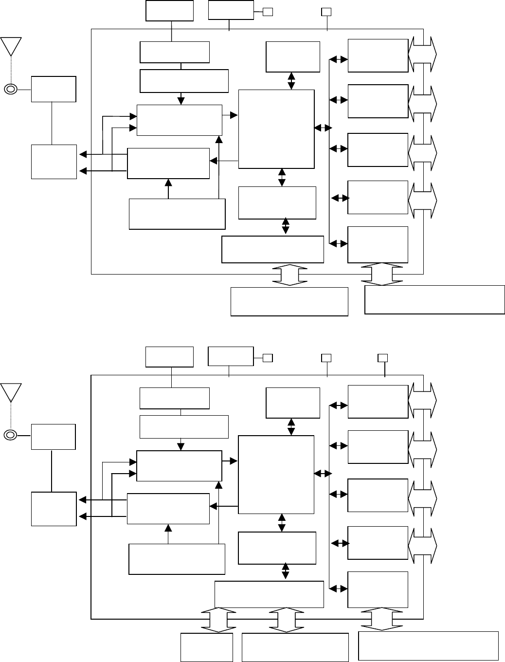
6. BLOCK DIAGRAM
6-1.WML-C09###
6-2.WML-C10###
UART
USB_D+
USB_D-
UART_TX
UART_RX
UART_RTS
UART_CTS
SPI_CSB
SPI_CLK
SPI_MOSI
SPI_MISO
PCM_OUT
PCM_IN
PCM_SYNC
PCM_CLK
SPI
PCM/IF
MEMORY
DRIVER
FLASH ROM (256kx16)
RAM
RF Receiver
RF Transmitter
1st Synthesizer
Baseband-
Controller
Memory-
Management
2nd Synthesizer
REG
16bits Micro-
Processor
XT Driver
16MHz VDD1
ANT
BPF
BC2-UART / BC2-USB
Balun
PIO [2],…,PIO [4]
USB
Programmable P/O
VDD2
UART
USB_D+
USB_D-
UART_TX
UART_RX
UART_RTS
UART_CTS
SPI_CSB
SPI_CLK
SPI_MOSI
SPI_MISO
PCM_OUT
PCM_IN
PCM_SYNC
PCM_CLK
SPI
PCM/IF
MEMORY
DRIVER
FLASH ROM (256kx16)
RAM
RF Receiver
RF Transmitter
1st Synthesizer
Baseband-
Controller
Memory-
Management
2nd Synthesizer
REG
16bits Micro-
Processor
XT Driver
16MHz VDD1
ANT
BPF
BC2-UART / BC2-USB
Balun
PIO [2],…,PIO [8]
USB
Programmable I/O
VDD2 VDD3
AIO [1]
7. PCM IF
PCM_OUT, PCM_IN, PCM_CLK, PCM_SYNC carry one of bi-directional channel of voice
data using 13bits PCM at 8ks/s.
PCM_SYNC operates at a fixed clock frequency of 8kHz.
PCM_CLK operates at a fixed clock frequency of 256kHz.
Bits 1 to 13 of the PCM_OUT data carry the current output sample value.
Bits 14 to 16 carry a three bit signal level value.
Reference PCM audio device is MC145483.
8. PIO PORT
The PIO port is general purpose IO interface and the ports consists of 8 programmable,
Bi-directional PIO [2:8] . The maximum current drive capability is 4mA.
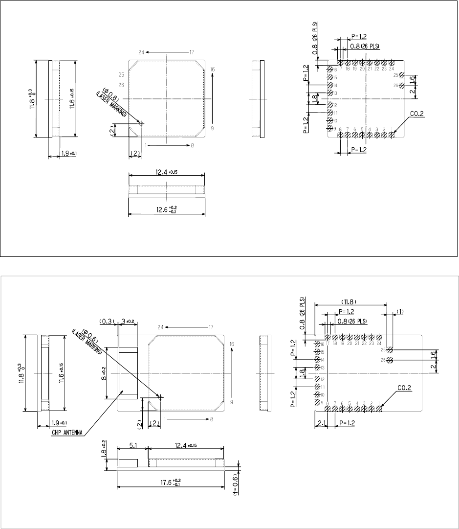
9. OVERALL APPEARANCE
9-1.WML-C09###
Module with antenna WML-C09A##
Module without antenna WML-C09N##
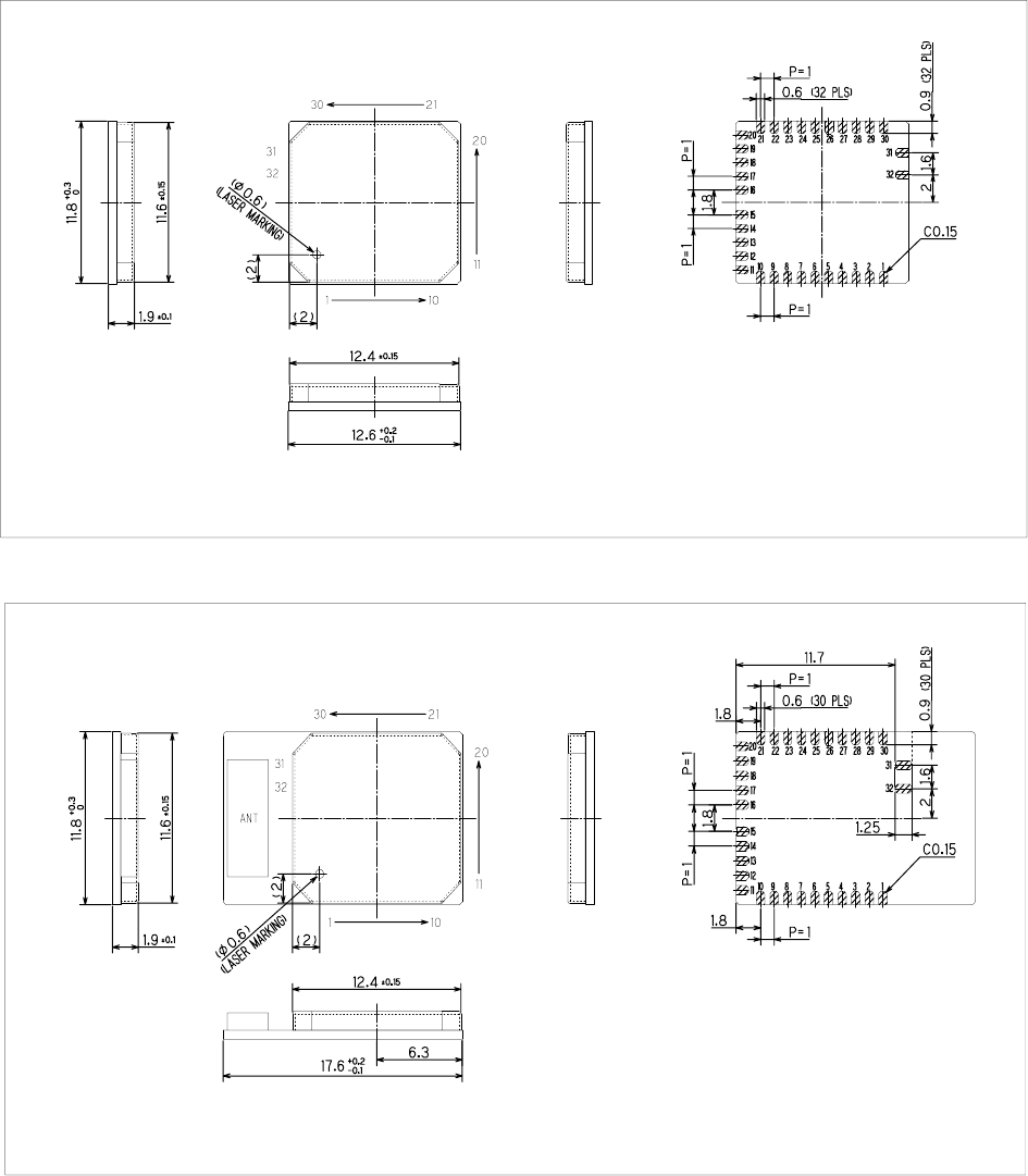
9-2.WML-C10###
Module with antenna WML-C10A##
Module without antenna WML-C10N##