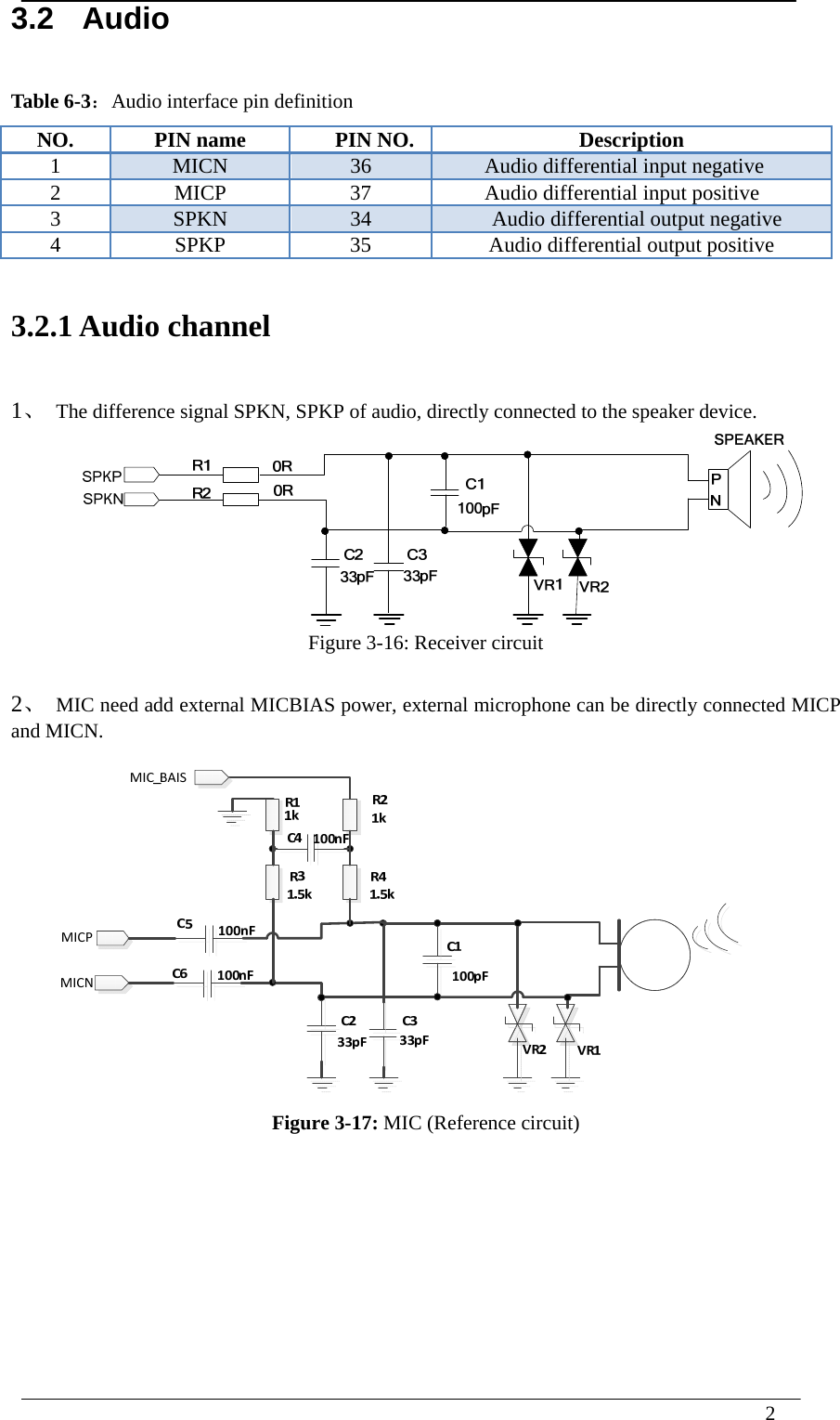
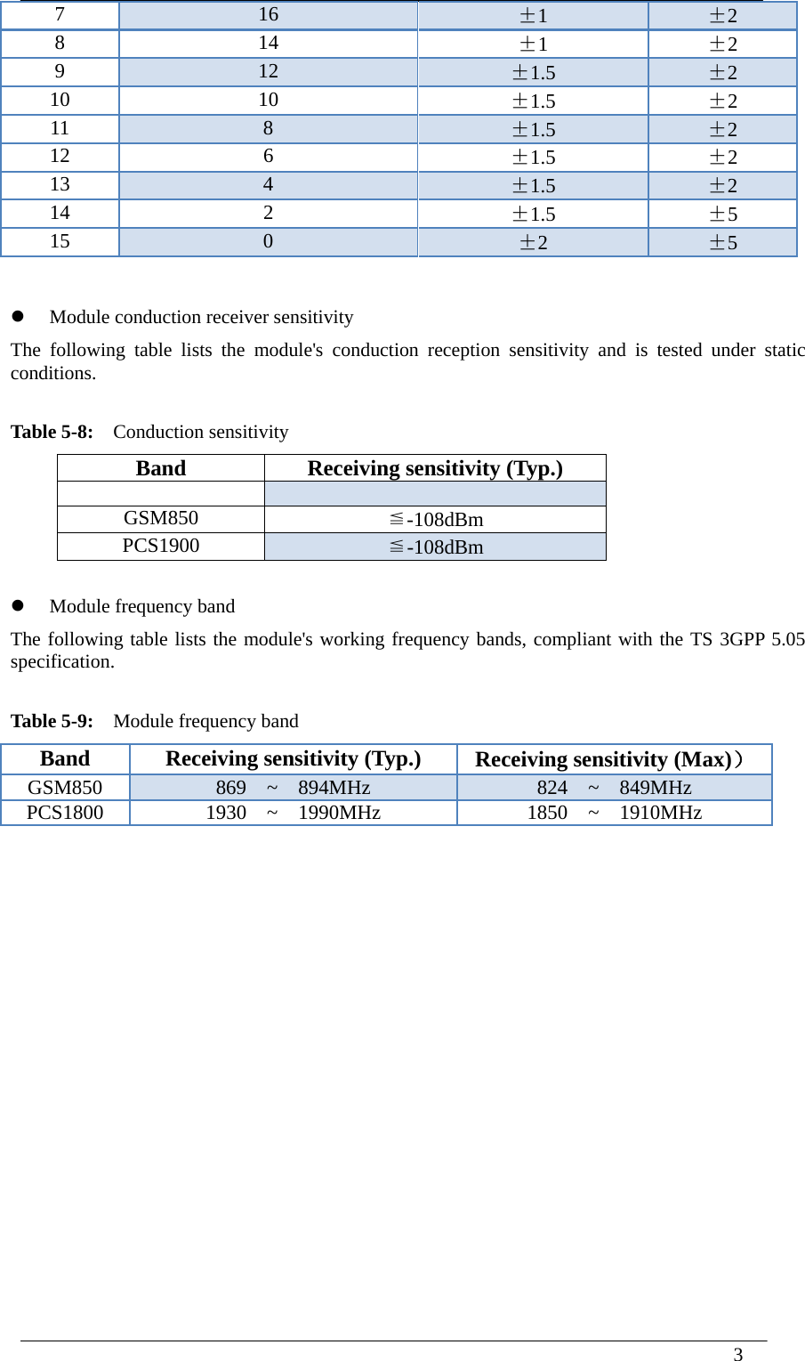
MobileTek Communication L218 GSM/GPRS+GNSS Module User Manual 001
Shanghai MobileTek Communication Ltd. GSM/GPRS+GNSS Module 001
UserManual.wiki
>
MobileTek Communication
>
L218 User Manual
15_L218 UserMan,r1
Navigation menu
Upload a User Manual
Namespaces
Wiki Guide
HTML
PDF
Info
Views
User Manual
Discussion / Help
Navigation
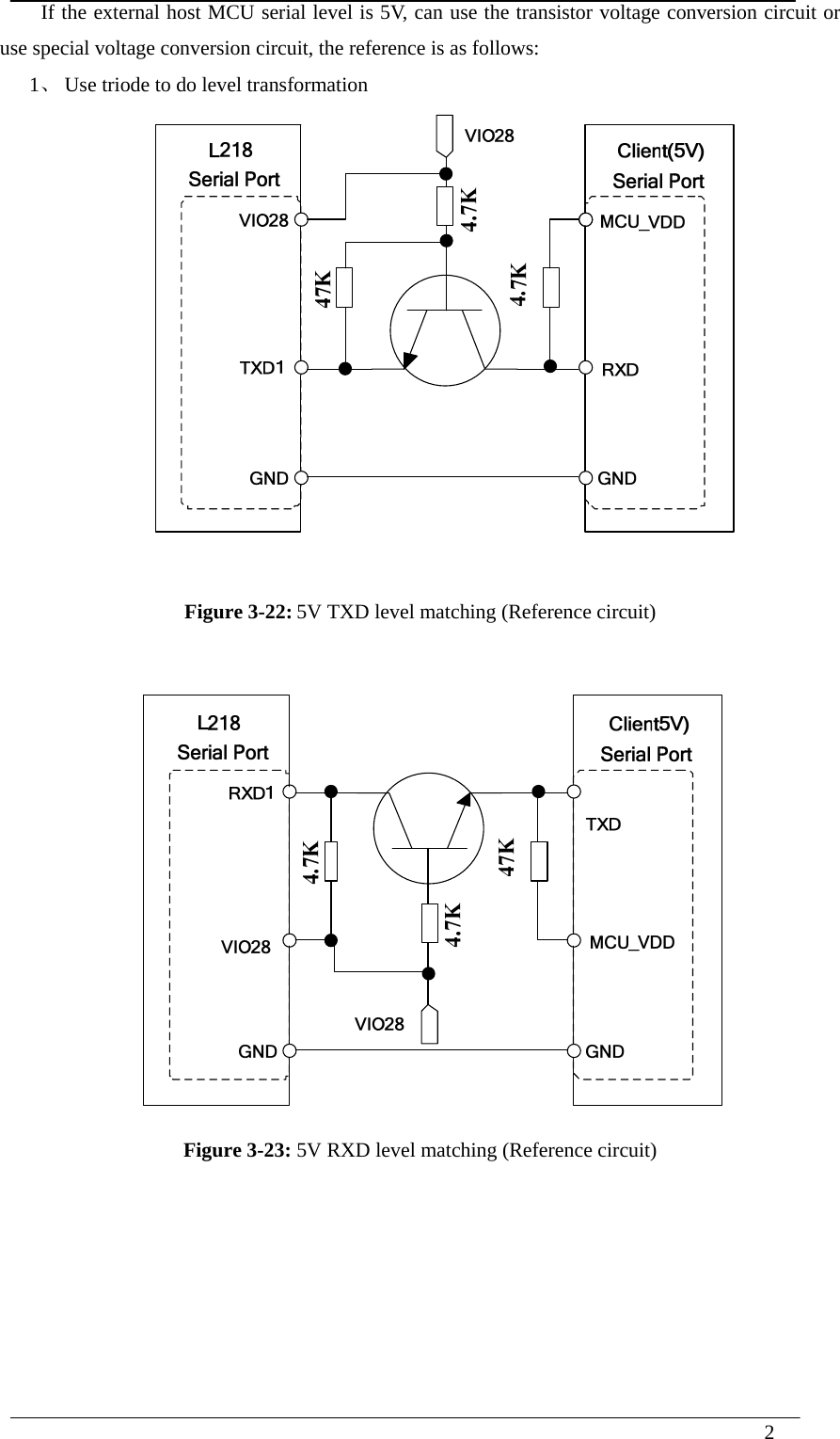
![2 The baud rate is fixed or adaptive baud rate synchronization settings. And send a command string "A-T" when serial ready after module will reply "OK". The host controller by sending "AT" command to the module, the module will automatically detect and identify the host controller's current baud rate. Adaptive baud rate function can make the host controller don't need to know the current baud rate and the module of communication will be finished. Adaptive baud rate function open by default. Adaptive baud rate operating configuration: Serial interface is configured to 8 bits of data bits, parity bits, one stop bit (the factory configuration). Adaptive baud rate mode, if there is no first synchronization module boot, such as "RDY", "+ CFUN: 1" and "+ CPIN: READY" URC information will not be reported. DTE in switching to a new baud rate, will first through the "AT" set up the new baud rate, before module detection and synchronous new baud rate, the module will use previous messages URC baud rate. DTE when switch to the new baud rate, the equipment is likely to receive unrecognized characters. Baud rates, is not recommended in a fixed mode switch to the adaptive baud rate model Note: the default module is adaptive baud rate (AT + IPR = 0), in the baud rate adaptive mode, after power on the URC information "RDY" will not back to the master machine. In the module boot after 2 ~ 3 seconds, can send the module AT commands. Master need to first send the "AT" the baud rate of character to the module to detect a master, and continue to send 1 ~ 5 "AT" string until module returns "OK". Then send a "AT + IPR = x & W" command to the module set the baud rate of a fixed, and save the configuration, after completed the configuration, each module after boot, will return to a URC information via a serial port "RDY". To further understand, please refer to the document [AT_DOCUMENT] "AT + IPR" in the chapter.](https://usermanual.wiki/MobileTek-Communication/L218/User-Guide-3315702-Page-21.png)
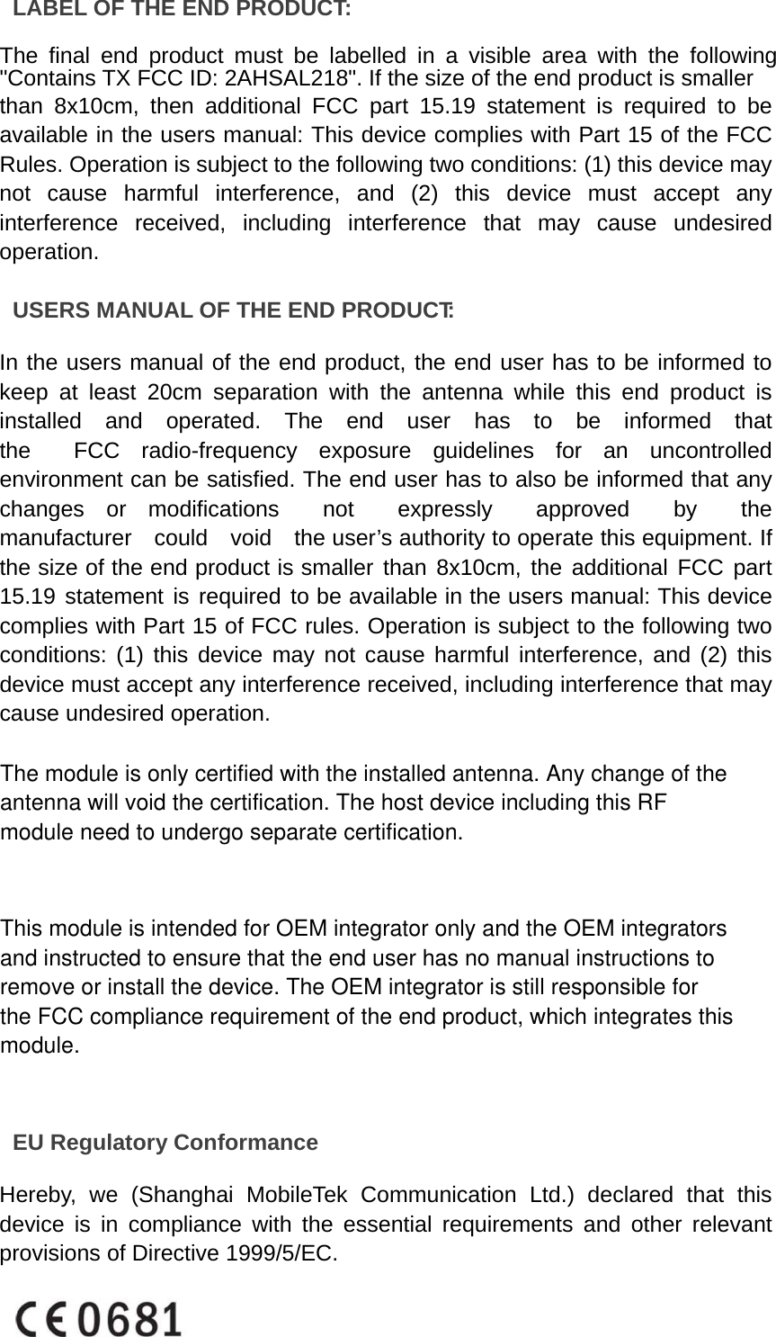
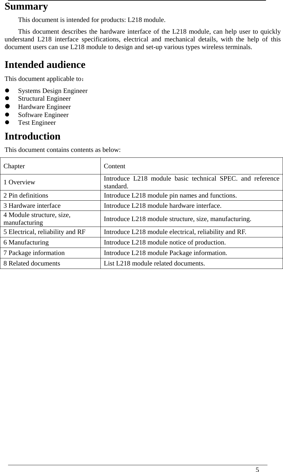
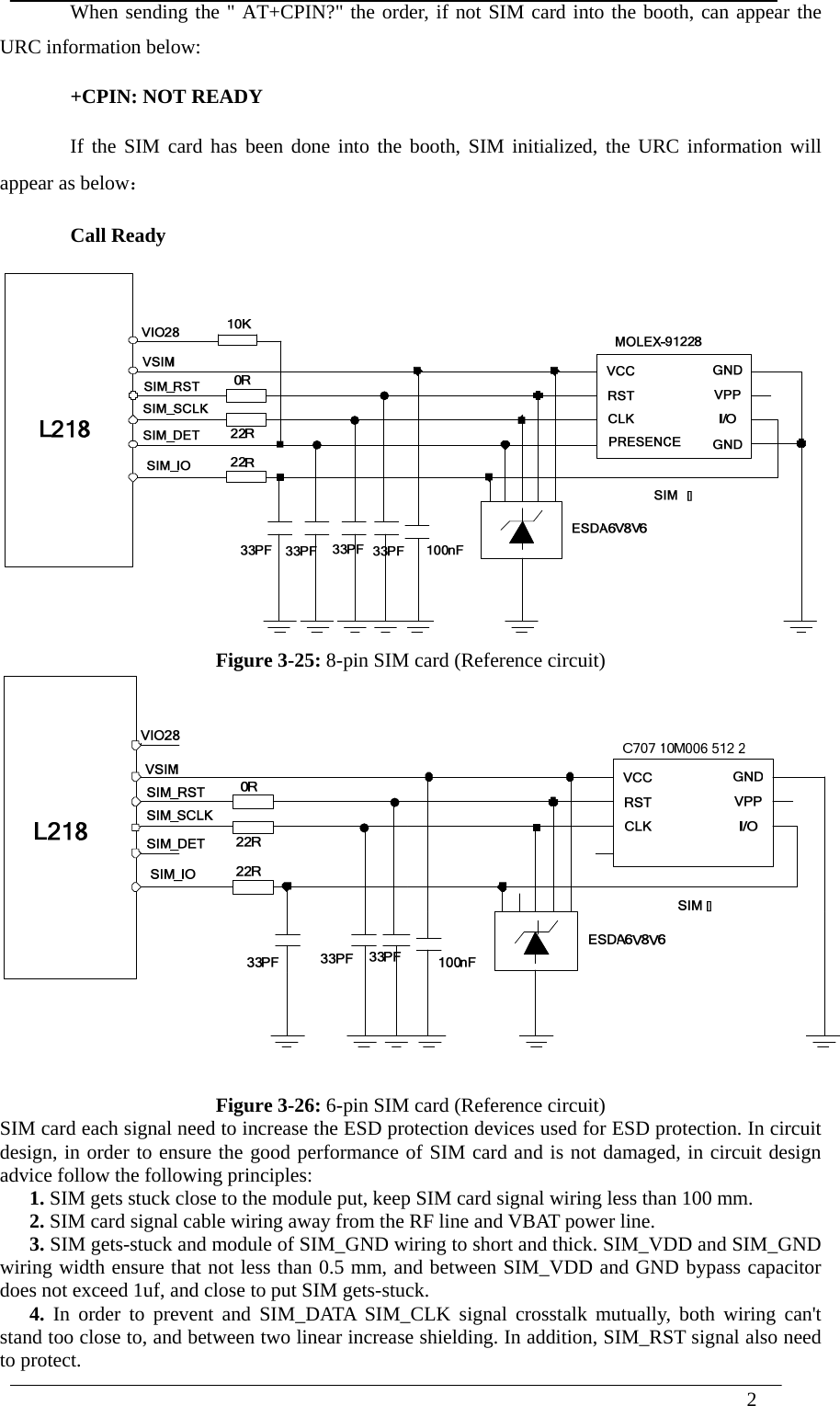
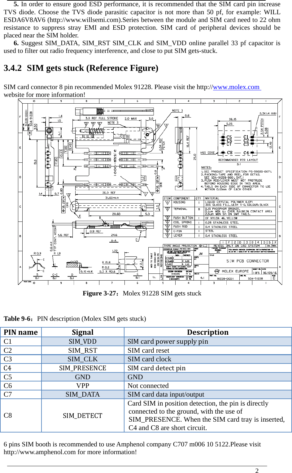
![2 2、Use FAIRCHILD to convert the chip NC7WZ07: Figure 3-24: Chip level matching (Reference circuit) 3.4 SIM Card Interface SIM card interface support GSM Phase1 specification function, also support the function of the GSM Phase 2 + specification and FAST 64 kbps SIM CARDS (for SIM application toolkit). SIM card supports 1.8V and 3.0V power supply through the internal power supply of the module. 3.4.1 SIM Interface Table 8-5:SIM card interface pin definition: NO.PINnamePINNO.Description1SIM_IO46SIMcarddataI/O2SIM_SCLK47SIM cardclock3SIM_RST1SIM cardreset4SIM_DET 3 SIM cardinsertdetectionpin 5VSIM2SIMpowersupply,accordingtothetypeofSIMcardautomaticallyselecttheoutputvoltage,3.0V10%or1.8V10%,theoutputcurrentofabout10mA.Below is a SIM card interface reference circuit, using 8 pin SIM gets stuck. SIM_DET pins for Molex SIM booth detection. When cato is inserted into the booth, SIM_DET into a low level. At this time whether or not a SIM card inside the cato, SIM_DET level from high to low make initialization module produces a SIM card. By default, the SIM card detection is off, you can use the "AT + ESIMS = 1" to open or "AT + ESIMS = 0" to close the function. Learn more about the content of the AT command, please refer to the document [AT_DOCUMENT].](https://usermanual.wiki/MobileTek-Communication/L218/User-Guide-3315702-Page-25.png)
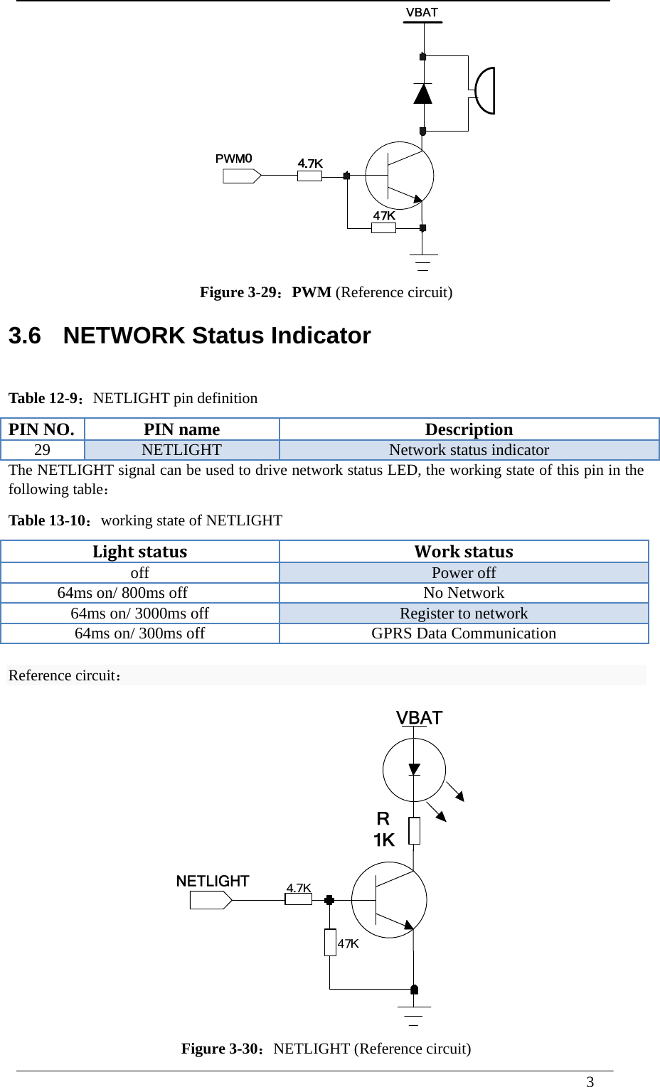
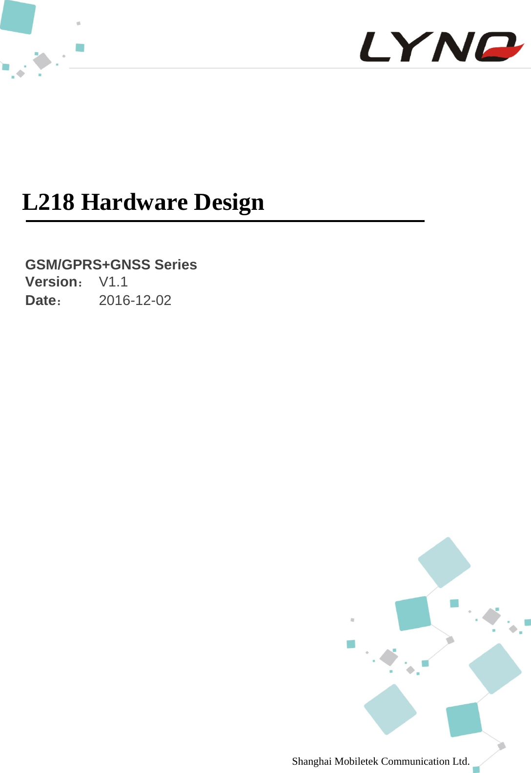
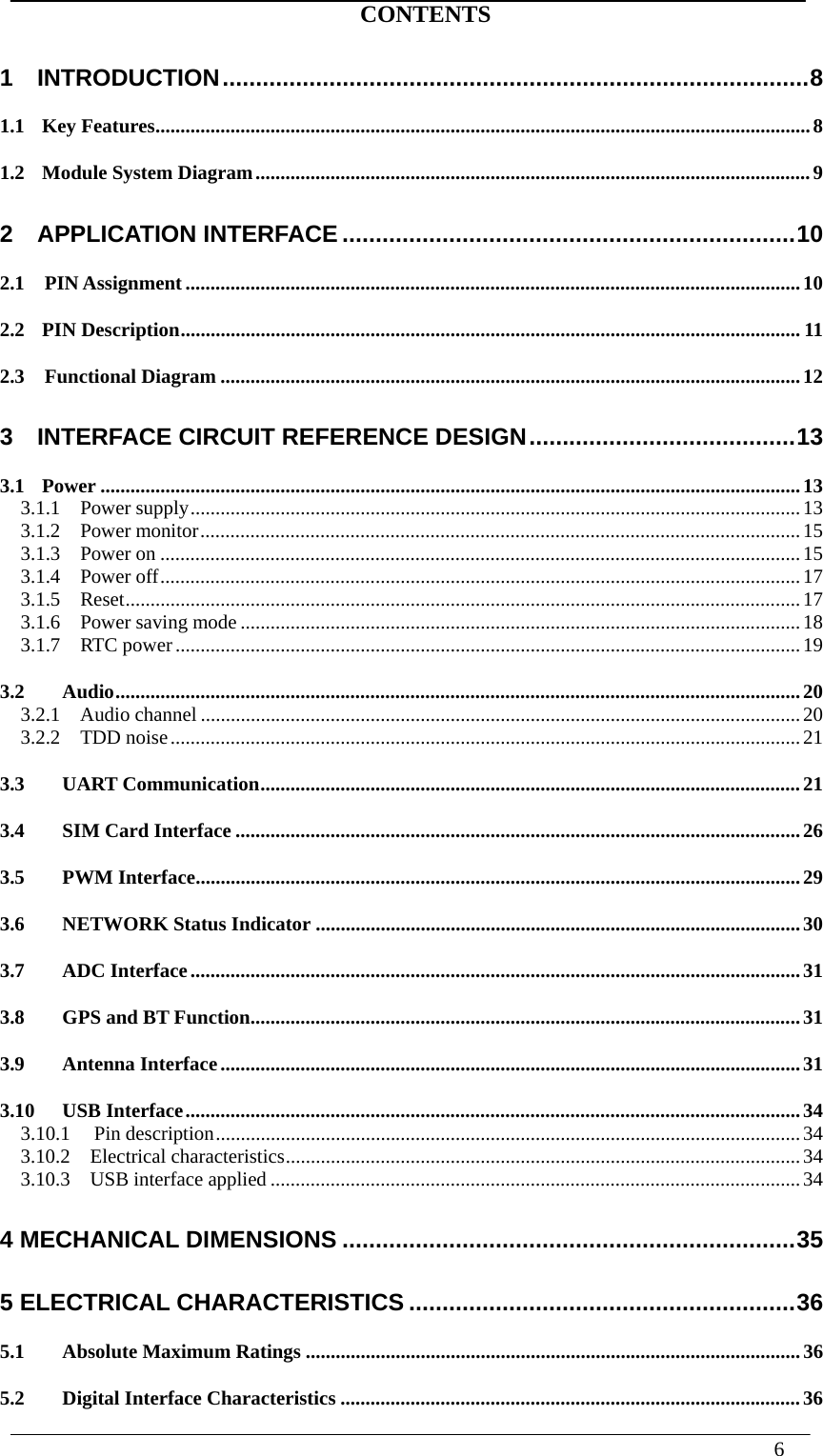
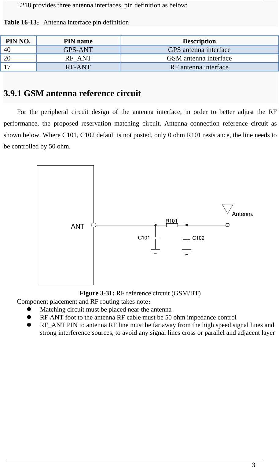
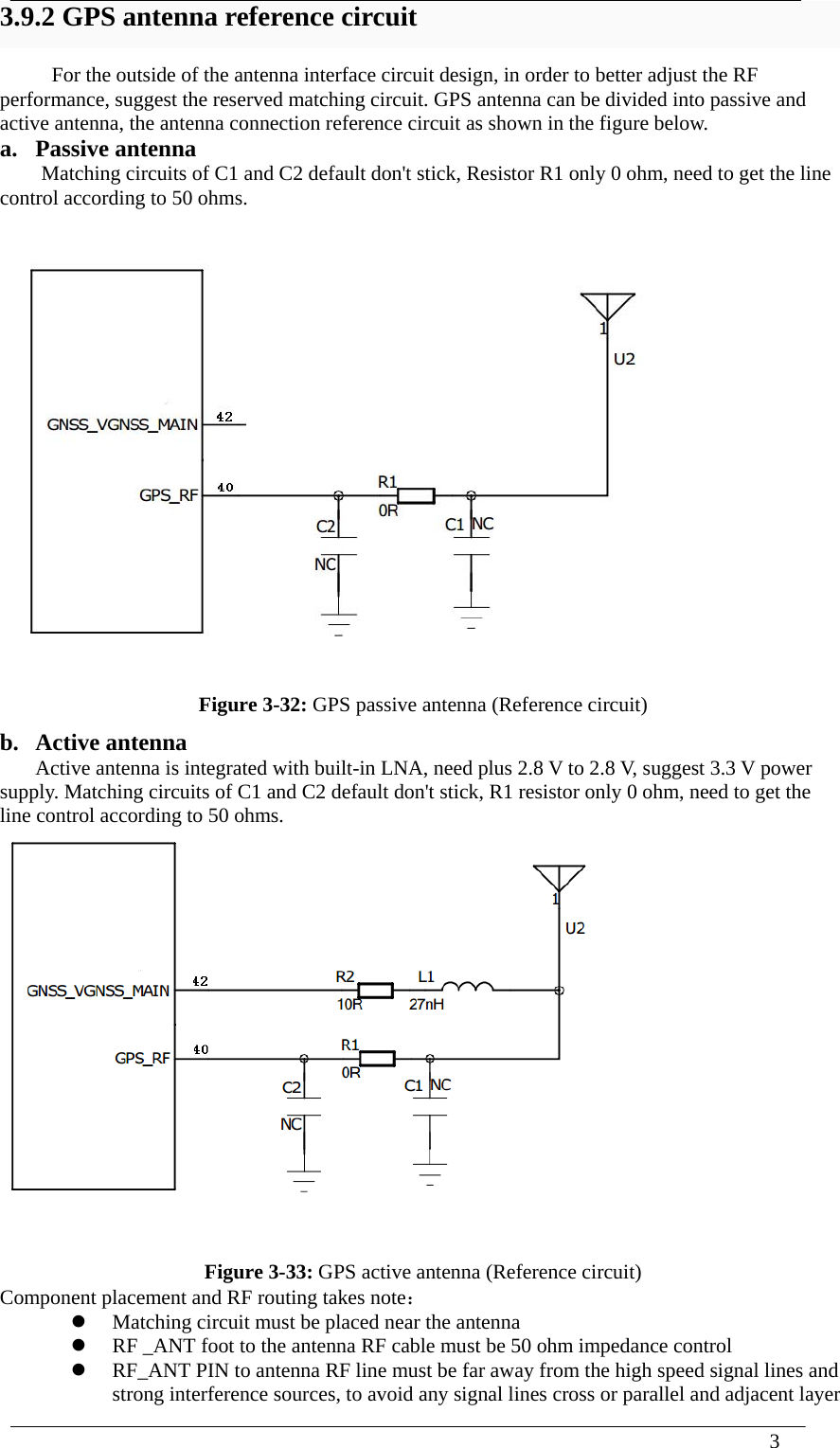
![3 3.7 ADC Interface L218 provides an ADC channel, the user can use the AT command "AT + CADC" to read voltage value on ADC pin. Note: the ADC sampling the voltage cannot be more than 2.8 V, otherwise easy to cause damage to the ADC. About the AT commands related information please refer to the document [AT_DOCUMENT]. In order to improve the accuracy of ADC, the layout of ADC should be surrounded by ground. Table 14-11:ADC interface pin definition PIN NO. PIN name Description 30 ADC Analog sampling Table 15-12:ADC Parameter Item Min Typ. Max Units Input voltage range 0 - 2.8 V ADC resolution - 10 - bits ADC sampling rate - - 1.0833 MHz ADC precision 10 30 mV 3.8 GPS Function L218 supports GPS, users only need external matching GPS antenna can be convenient to use this feature. Can use AT commands through the serial port to the GPS operation, in order to realize positioning, and other functions. 3.9 Antenna Interface L218 interface provides three antenna, GSM antenna interface RF_ANT respectively, and the GPS antenna interface GPS_RF ANT_RF antenna and interface. GPS antenna, GSM antenna, RF antenna working in choose all needs to choose frequency band input impedance of 50 ohm, standing wave coefficient is less than 2 antenna products. As far as possible away from two kinds of antenna is placed. Each port antenna and other port isolation ratio should be greater than 30 dB.](https://usermanual.wiki/MobileTek-Communication/L218/User-Guide-3315702-Page-30.png)
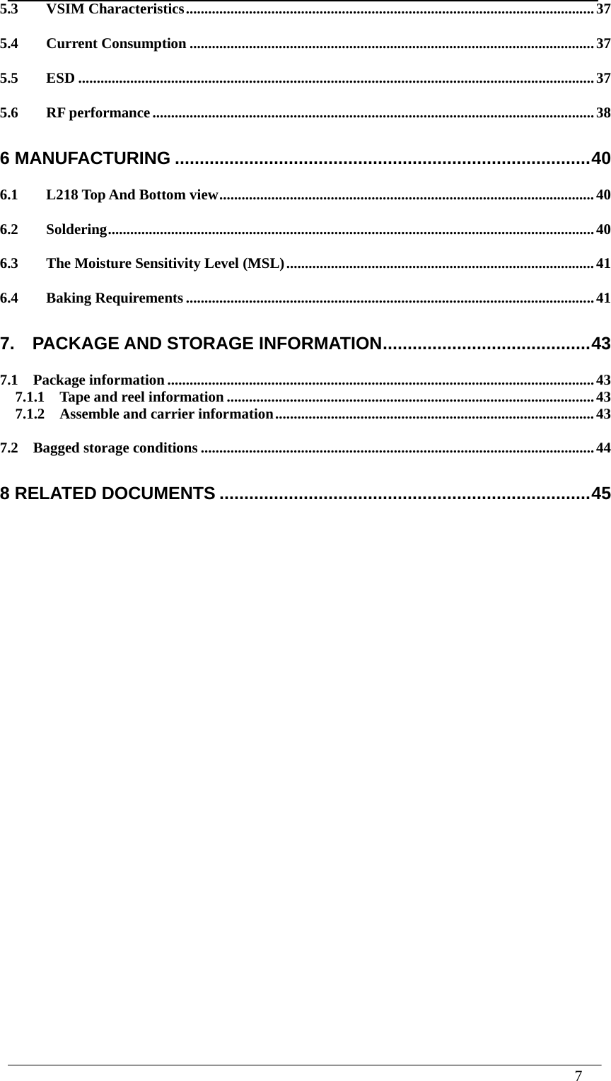
![4 8 RELATED DOCUMENTS Table 8-1:Related documents NO. Documents Note [1] AT_DOCUMENT [2] ITU-T Draft new recommendation V.25ter:Serial asynchronous automatic dialing and control [3] GSM 07.07: Digital cellular telecommunications (Phase 2+); AT command set for GSM Mobile Equipment (ME) [4] GSM 07.10: Support GSM 07.10 multiplexing protocol [5] GSM 07.05: Digital cellular telecommunications (Phase 2+); Use of Data Terminal Equipment – Data Circuit terminating Equipment (DTE – DCE) interface for Short Message Service (SMS) and Cell Broadcast Service (CBS) [6] GSM 11.14: Digital cellular telecommunications system (Phase 2+); Specification of the SIM Application Toolkit for the Subscriber Identity Module – Mobile Equipment (SIM – ME) interface [7] GSM 11.11: Digital cellular telecommunications system (Phase 2+); Specification of the Subscriber Identity Module – Mobile Equipment (SIM – ME) interface](https://usermanual.wiki/MobileTek-Communication/L218/User-Guide-3315702-Page-44.png)