MobileTek Communication L218 GSM/GPRS+GNSS Module User Manual 001
Shanghai MobileTek Communication Ltd. GSM/GPRS+GNSS Module 001
15_L218 UserMan,r1

2
L218 Hardware Design
GSM/GPRS+GNSS Series
Version: V1.1
Date: 2016-12-02
Shanghai Mobiletek Communication Ltd.

3
Notice
Some features of the product and its accessories described herein rely on the software installed,
capacities and settings of local network, and therefore may not be activated or may be limited by
local network operators or network service providers.
Thus, the descriptions herein may not exactly match the product or its accessories which you
purchase. Shanghai Mobiletek Communication Ltd reserves the right to change or modify any
information or specifications contained in this manual without prior notice and without any liability.
Copyright
This document contains proprietary technical information which is the property of Shanghai
Mobiletek Communication Ltd. copying of this document and giving it to others and the using or
communication of the contents thereof, are forbidden without express authority. Offenders are liable
to the payment of damages. All rights reserved in the event of grant of patent or the registration of a
utility model or design. All specification supplied herein are subject to change without notice at any
time.
DISCLAIMER
ALL CONTENTS OF THIS MANUAL ARE PROVIDED “AS IS”. EXCEPT AS REQUIRED BY
APPLICABLE LAWS, NO WARRANTIES OF ANY KIND, EITHER EXPRESS OR IMPLIED,
INCLUDING BUT NOT LIMITED TO, THE IMPLIED WARRANTIES OF MERCHANTABILITY
AND FITNESS FOR A PARTICULAR PURPOSE, ARE MADE IN RELATION TO THE
ACCURACY, RELIABILITY OR CONTENTS OF THIS MANUAL.
TO THE MAXIMUM EXTENT PERMITTED BY APPLICABLE LAW, IN NO EVENT SHALL
SHANGHAI MOBILETEK COMMUNICATION LTD BE LIABLE FOR ANY SPECIAL,
INCIDENTAL, INDIRECT, OR CONSEQUENTIAL DAMAGES, OR LOSS OF PROFITS,
BUSINESS, REVENUE, DATA, GOODWILL SAVINGS OR ANTICIPATED SAVINGS
REGARDLESS OF WHETHER SUCH LOSSES ARE FORSEEABLE OR NOT.

4
Version History
Date Version Description of change Author
2016-09-28 V1.0 Initial
2016-12-02 V1.1 Modify the figure and table. Add the packing
instructions Ren xue

5
Summary
This document is intended for products: L218 module.
This document describes the hardware interface of the L218 module, can help user to quickly
understand L218 interface specifications, electrical and mechanical details, with the help of this
document users can use L218 module to design and set-up various types wireless terminals.
Intended audience
This document applicable to:
Systems Design Engineer
Structural Engineer
Hardware Engineer
Software Engineer
Test Engineer
Introduction
This document contains contents as below:
Chapter Content
1 Overview Introduce L218 module basic technical SPEC. and reference
standard.
2 Pin definitions Introduce L218 module pin names and functions.
3 Hardware interface Introduce L218 module hardware interface.
4 Module structure, size,
manufacturing Introduce L218 module structure, size, manufacturing.
5 Electrical, reliability and RF Introduce L218 module electrical, reliability and RF.
6 Manufacturing Introduce L218 module notice of production.
7 Package information Introduce L218 module Package information.
8 Related documents List L218 module related documents.

6
CONTENTS
1 INTRODUCTION ........................................................................................ 8
1.1Key Features ................................................................................................................................... 8
1.2Module System Diagram ............................................................................................................... 9
2 APPLICATION INTERFACE .................................................................... 10
2.1 PIN Assignment ........................................................................................................................... 10
2.2PIN Description ............................................................................................................................ 11
2.3 Functional Diagram .................................................................................................................... 12
3 INTERFACE CIRCUIT REFERENCE DESIGN ........................................ 13
3.1Power ............................................................................................................................................ 13
3.1.1 Power supply .......................................................................................................................... 13
3.1.2 Power monitor ........................................................................................................................ 15
3.1.3 Power on ................................................................................................................................ 15
3.1.4 Power off ................................................................................................................................ 17
3.1.5 Reset ....................................................................................................................................... 17
3.1.6 Power saving mode ................................................................................................................ 18
3.1.7 RTC power ............................................................................................................................. 19
3.2Audio ......................................................................................................................................... 20
3.2.1 Audio channel ........................................................................................................................ 20
3.2.2 TDD noise .............................................................................................................................. 21
3.3UART Communication ............................................................................................................ 21
3.4SIM Card Interface ................................................................................................................. 26
3.5PWM Interface ......................................................................................................................... 29
3.6NETWORK Status Indicator ................................................................................................. 30
3.7ADC Interface .......................................................................................................................... 31
3.8GPS and BT Function .............................................................................................................. 31
3.9Antenna Interface .................................................................................................................... 31
3.10USB Interface ........................................................................................................................... 34
3.10.1Pin description ..................................................................................................................... 34
3.10.2 Electrical characteristics ....................................................................................................... 34
3.10.3 USB interface applied .......................................................................................................... 34
4 MECHANICAL DIMENSIONS .................................................................... 35
5 ELECTRICAL CHARACTERISTICS .......................................................... 36
5.1Absolute Maximum Ratings ................................................................................................... 36
5.2Digital Interface Characteristics ............................................................................................ 36

7
5.3VSIM Characteristics .............................................................................................................. 37
5.4Current Consumption ............................................................................................................. 37
5.5ESD ........................................................................................................................................... 37
5.6RF performance ....................................................................................................................... 38
6 MANUFACTURING .................................................................................... 40
6.1L218 Top And Bottom view ..................................................................................................... 40
6.2Soldering ................................................................................................................................... 40
6.3The Moisture Sensitivity Level (MSL) ................................................................................... 41
6.4Baking Requirements .............................................................................................................. 41
7. PACKAGE AND STORAGE INFORMATION .......................................... 43
7.1 Package information ................................................................................................................... 43
7.1.1 Tape and reel information ................................................................................................... 43
7.1.2 Assemble and carrier information ...................................................................................... 43
7.2 Bagged storage conditions .......................................................................................................... 44
8 RELATED DOCUMENTS ........................................................................... 45

8
1 INTRODUCTION
L218 is a quad-band GSM/GPRS+GNSS module, working frequency:
GSM/GPRS850/900/1800/1900 MHz.
With a tiny package of 14.5mm x 18.5mm x 2.3mm, L218 fits all the applications, such as M2M,
smart phone, PDA, etc.
It is a 47-pin SMT pad module, which provides rich hardware interfaces. It supports voice, SMS
and data transmission with low power consumption.
1.1 Key Features
Table 1-1: Main Feature
GSM quad-band: 850/1900 MHz
GSM 2/2+ standard
– Class 4(2 W @ 850 MHz)
– Class 1(1 W @ 1900MHz)
AT command (GSM 07.07 ,07.05 and Enhanced AT command set)
Power supply: 3.4 ~4.2V(Recommended 3.8V)
Operating temperature: -40~+85℃
Storage temperature: -45~+90℃
weight:1g
Data Transmission Coding schemes CS 1, 2, 3, 4
PPP‐stac
k
Supportpass‐through
SMS Point to Point MO and MT
SMS status report
Text and PDU
Voice Half Rate(HR)
Full Rate(FR)
Text and PDU mode
Enhanced Full Rate(EFR)
Adaptive-negotiation Multi-code Rate(AMR)
GNSS
Receivertype:33tracking/99captured
Maximumupdaterate:10Hz
Sensitivity
‐‐Tracking:‐165dBm
-- Reacquisition:‐160dBm
‐‐Coldstarts:‐148dBm
Time‐To‐Firs
t
‐Fix
‐‐Coldstart:31s(typical)
‐‐Warmstart:26s
‐‐Hotstarts:<1s
‐‐EPOAssist:13s(CTTFF)
Accuracy
‐‐AutomaticPosition:2.5mCEP
‐‐Speed:0.1m/s
9
Interface
47 SMT pads(Stamps Holes)
One analog audio
One serial interfaces
One SIM card interface (3V/ 1.8V)
One ADC interface
GPIO interface
USBinterface
GSM antenna pad
GPS antenna pad
1.2 Module System Diagram
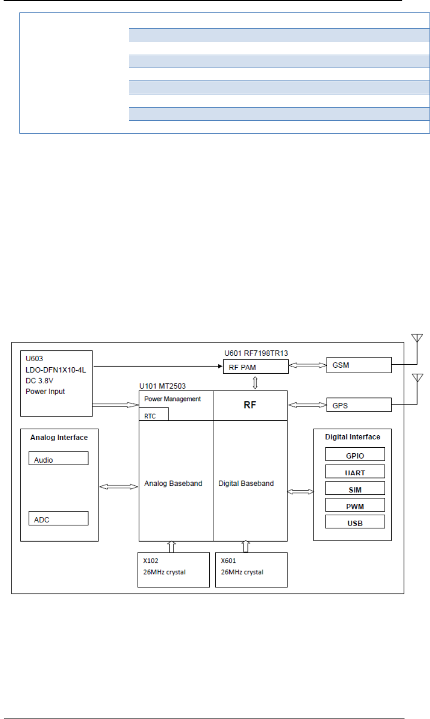
Following figure: List main function of module
GSM Baseband and RF
Power Management
Antenna Interface
Other interfaces
Figure 1-1:Module function diagram
1
2 APPLICATION INTERFACE
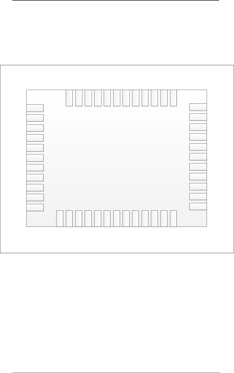
2.1 PIN Assignment
Figure 1-1: L218 Pin out diagram (TOP View)
Interfaces as below:
Analog voice: One MIC inputs, one speaker output.
USB: USB interface.
SIM card: support 1.8V and 3V.
Reset: Support RESETB pin to reset the module.
GPIO:PIN 23 for normal general purpose in/out, and some other pins can be configured as
GPIO pin (detail information in the following table).
Serial port:Contain one full functional serial interface, CTS and RTS etc. should be NC when
not used.
RF: GSM,GPS
L218LCC
TOP
1
2
3
4
5
6
7
8
9
10
11
23
22
21
20
19
18
17
16
15
14
13
12
24
35
34
33
32
31
30
29
28
27
26
25
37
38
39
40
41
42
43
44
45
46
47
36
SPKP
SPKN
VRTC
RESETB
PWRKEY
ADC
NETLIGHT
STATUS
GND
VBAT
VBAT
GND
GND
RF_ANT
GND
GND
BT_ANT
GND
VIO28
PWM0
GPS_UARTTXD
RESERVED
SIM_RST
VSIM
SIM_DET
TXD1
RXD1
DTR1
RING1
RTS1
DSR1
CTS1
DCD1
GPIO_MB_0
GND
SIM_SCLK
SIM_IO
USB_DP
USB_DM
USB_VBUS
VCC_RF_GPS
GND
GPS_RF
GND
RESERVED
MICP
MICN

1
2.2 PIN Description
L218 PIN description as below:
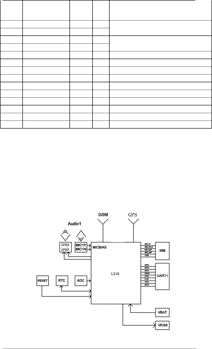
Table 2-1: PIN description
PIN
NO. PIN name Type* Reset Function Description
1 SIM_RST I/O PD SIM signal
2 VSIM POWER / SIM signal
3 SIM_DET I/O PD SIM signal
4 TXD1 O PU
Request to Send, For AT command, firmware
upgrades and data transmission.
5 RXD1 I PU
Receive data, For AT command, firmware
upgrades and data transmission.
6 DTR1 I PD
Data terminal ready (Control module wake or
sleep)
7 RING1 O PD Ring indicator
8 RTS1 O PU Request to Send
9 DSR1 O PD Data Set Ready
10 CTS1 I PU Clear to send
11 DCD1 O PD Data carrier detect
12 REVERSED I/O PD General purpose input/output
13 GPS_UARTTXD I/O PD GPS NEMA Output
14 PWM0 I/O PD PWM output
15 VIO28 POWER / VDDIO 2.8V output, max current is 20mA
16 GND GND / GND
17 RF ANT I/O / RF Antenna
18 GND GND / GND
19 GND GND / GND
20 RF_ANT / / GSM Antenna
21 GND GND / GND
22 GND GND / GND
23 GPIO_MB_0 I/O PD General purpose input/output
24 GND GND / GND
25 VBAT POWER /
Power supply. The power supply range is from
3.4V to 4.2V. Recommended voltage is 3.8V.
26 VBAT POWER /
27 GND GND / GND
28 STATUS O / Running status indicator
29 NETLIGHT I/O PD Net status indicator
30 ADC AI /
Analog to digital conversion interface,Max
voltage is 2.8V.
31 PWRKEY AI /
PWRKEY should be pulled low at least 1
second and then released to power on/down the
module
32 RESETB I / Reset signal,internal pulled up to1.8V.
1
33 VRTC POWER /
RTC voltage, input 2.8V, maximum current of
2mA. External button battery or a large
capacitor, If no use can be set NC
34 SPKN AO /
Differential audio output.
35 SPKP AO /
36 MICN AI /
Differential input, with internal bias voltage.
37 MICP AI /
38 REVERSED POWER MIC Bias output
39 GND GND / GND
40 GPS_RF / / FM Antenna
41 GND GND / GND
42 VCC_RF_GPS POWER / GPS Power Output
43 USB_VBUS I / USB Power
44 USB_DM I/O / USB Differential data D-
45 USB_DP I/O / USB Differential data D+
46 SIM_IO I/O PD SIM signal
47 SIM1_SCLK I/O PD SIM signal
* Type I , O , I/O can be configured as general GPIO, its status is PU or PD when reset.
* The high level of the digital signal is 2.8V (min:2.6V, max3.0V).
2.3 Functional Diagram
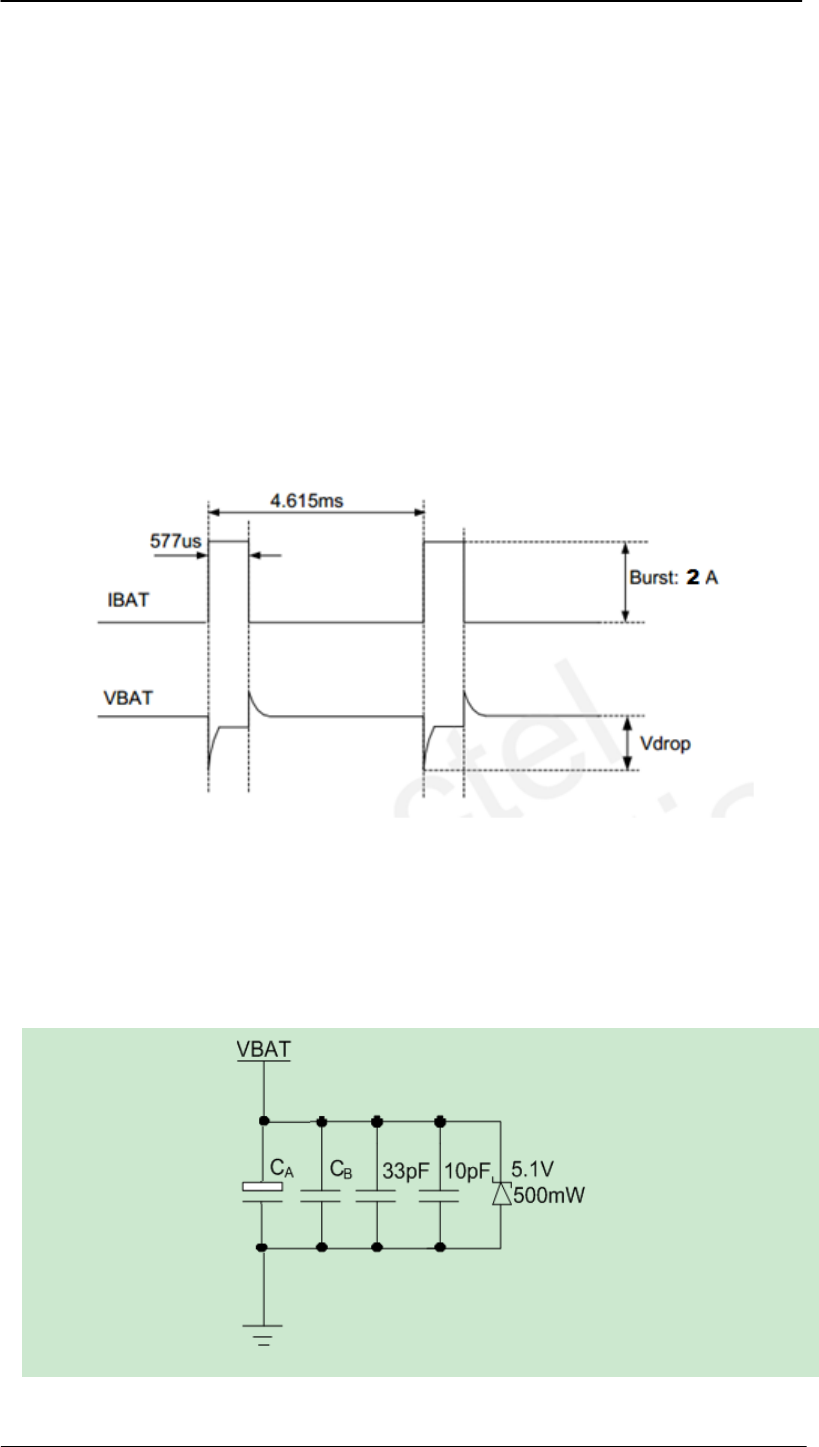
Main function of module PINs listed as below
SIM card interface
Audio interface
Antenna interface
Other interfaces
Figure 3-2: Function diagram
1
3 INTERFACE CIRCUIT REFERENCE DESIGN
3.1 Power
3.1.1 Power supply
VBAT is the main power source of L218 module., from 3.4V to 4.2V, and 3.8V is the
recommended voltage. In GSM system, RF signal works in burst transmit, a continuous 577us (1/8 of
a TDMA period) burst will be found at intervals of 4.615ms. In burst period, peak current is
necessary to make sure operating voltage won’t drop to the base one. Because when module is
working under the base voltage, the burst will cause VBAT has instantaneous large current, which the
peak value could reach 2A or above and lead to the Vdrop about 350mV.
Figure 3-1:Module burst current and voltage waveforms
It is recommended to use a large capacitor close to VBAT PIN. The capacitor is the bigger the
better to improve power stability. 470uF or more low-ESR aluminum electrolytic capacitors is
recommended for CA. If the lithium battery directly connected, 220uF or 100uF tantalum capacitor
(low ESR) is recommended for CB. The capacitors of 33pF and 10pF in parallel can effectively
remove high-frequency interference. The capacitors should close to the VBAT pin of module.
Figure 3-2: VBAT input (Reference circuit)
1
It is strongly recommended to add a 5.1V / 500mW Zener diode to VBAT pin in parallel, Zener
diode should close to the VBAT pin. Recommended parts list as below:
Table 4-1: Recommended Zener diode
Vendor Factory Model Power Encapsulation
On semi MMSZ5231BT1G 500mW SOD123
JCST MMSZ5231B 500mW SOD123
Prisemi PZ5D4V2H 500mW SOD523
ROHM HDZMV4Z015.1B 500mW UMD2
SIG SIG1Z5T1G 500mW SOD323
Vishay MMSZ4689-V 500mW SOD123
Crownpo CDZ55C5V1SM 500mW 0805
NOTE: TVS must has a good GND nearest to interface. VRWM value cannot be too high, normally it
is the 1/3 added one based on its own voltage value
If the power supply is over 4.2V, voltage conversion is required, LDO or Buck chipset can do
that function.
1、 As the LDO efficiency is closely related to the input/output dropout voltage value, the
greater the voltage difference, the lower the efficiency, and at the same time, the problem of heat
radiation will be detected, there is a demand of the small dropout voltage between DC input and
LDO output. For instance, the voltage difference between 5V input and 4.1V output is
acceptable.
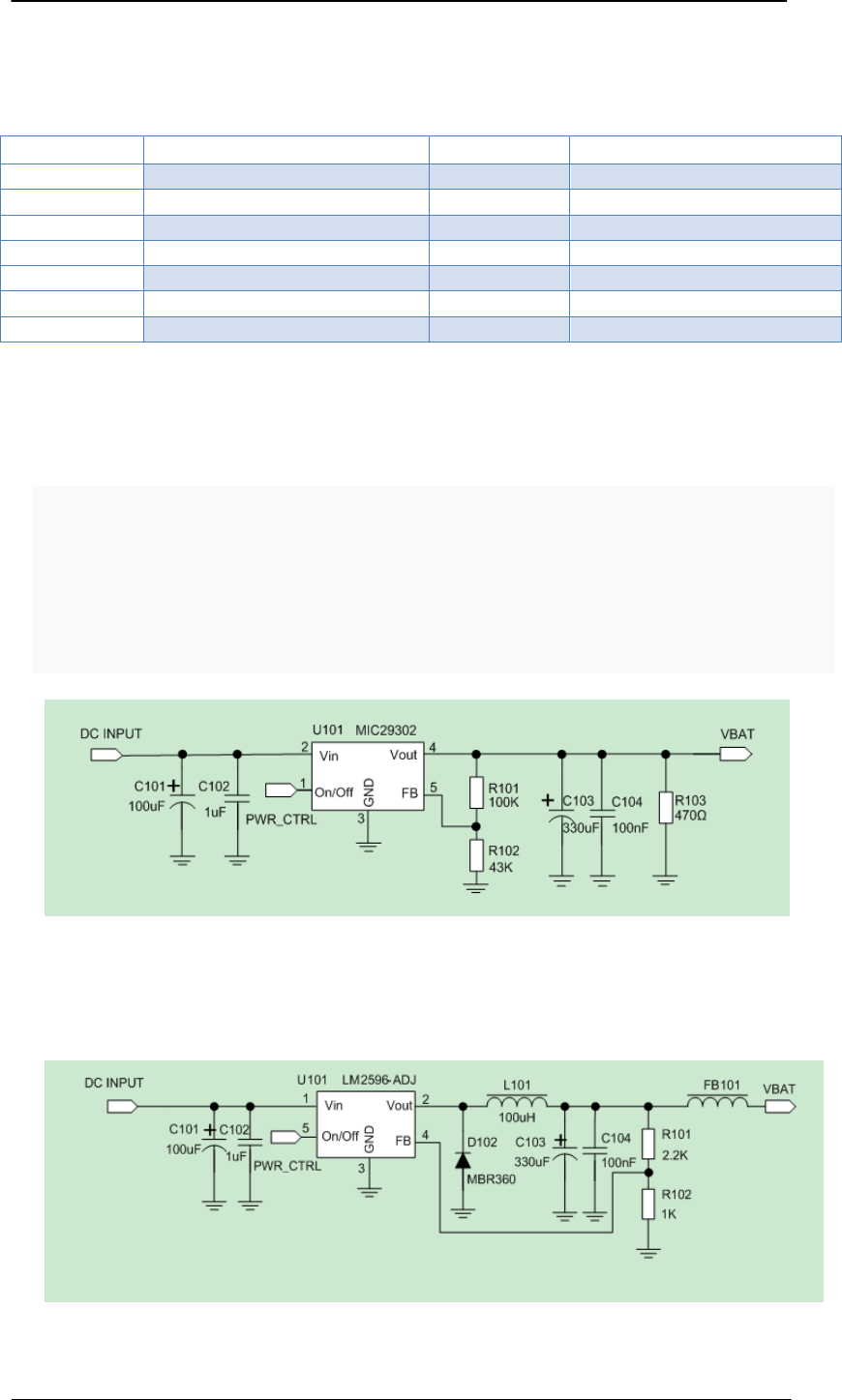
The reference power supply circuit design with LDO is shown as figure below:
Figure 3-3:LDO (Reference circuit)
2、Buck circuit can enhance the conversion rate if the differential value is great. But meanwhile,
the EMI issue caused by DCDC will be concerned.
Figure 3-4:DC-DC (Reference circuit)
1
3、PMOS control circuit for power switch.
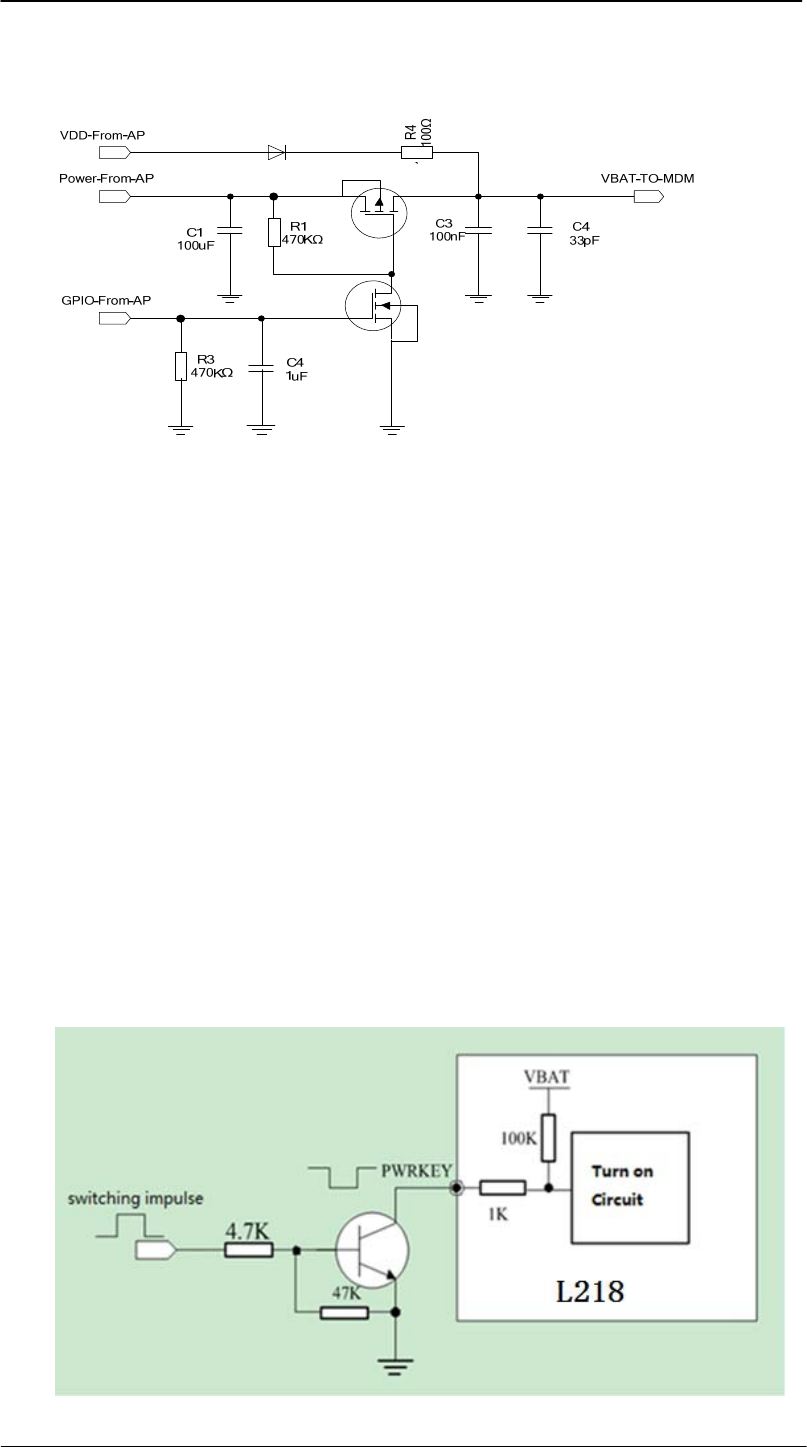
If want to control VBAT under the circumstance that there is no need of power conversion, for
example, lithium-ion battery is the direct power supply, PMOS control circuit can be the choice.
Figure 3-5:PMOS (Reference circuit)
3.1.2 Power monitor
To monitor the power supply voltage, you can use " AT+CBC " command. For details,
you can refer to AT command manual.
3.1.3 Power on
Module to normal boot mode is through lower PWRKEY pin at least 1 second. After successful
boot PWRKEY pin can be released. NETLIGHT signal can be used to determine whether module
boot. When NETLIGHT start according to certain frequency output pulse signal, if connect lights,
lights flashing, suggests that successful boot module. If no output pulse signal, has been as low level,
no boot mod.
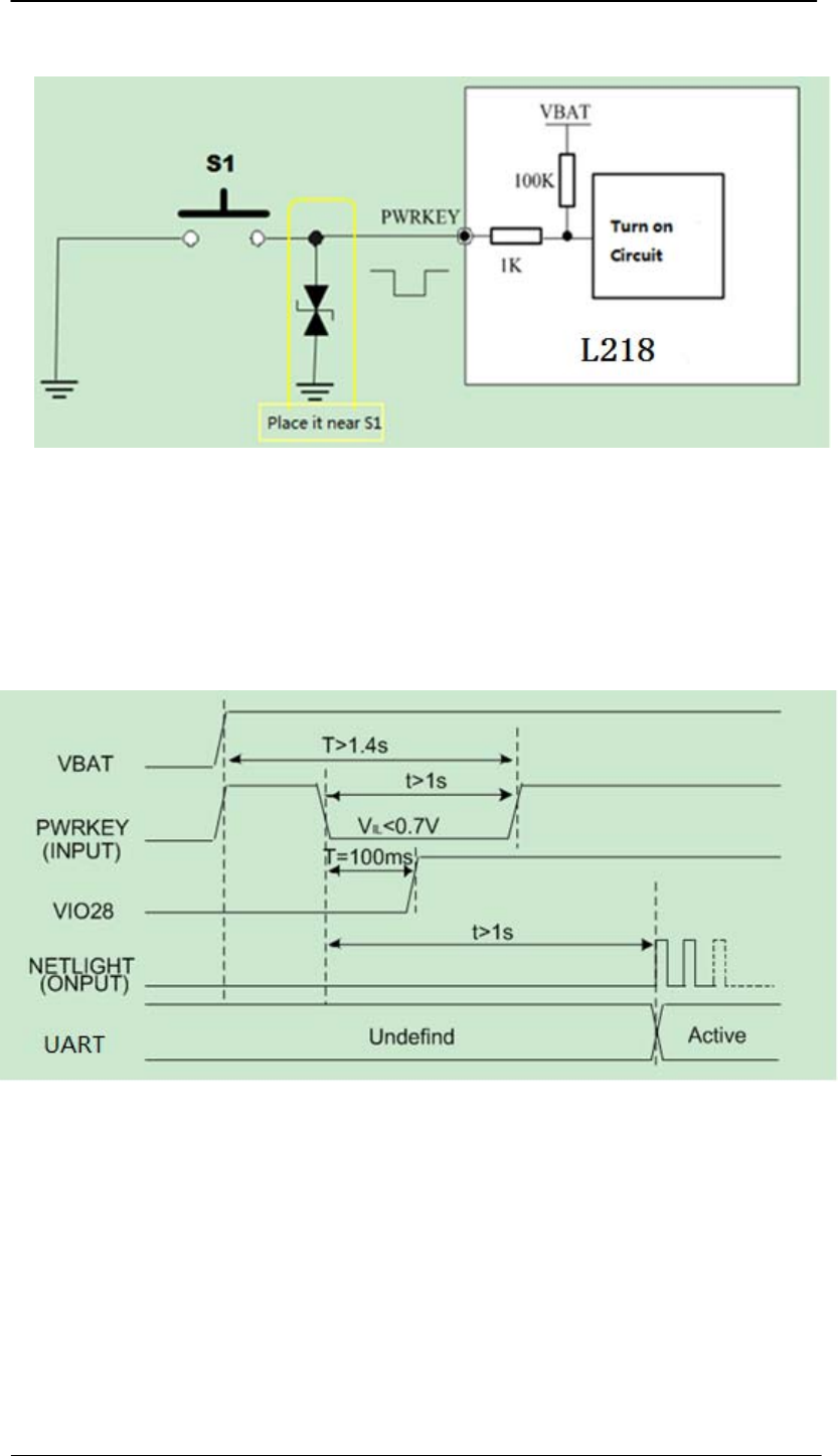
Recommend the following boot circuit (PWRKEY came on the module VBAT). The reference circuit
is as follows:
1、With triode control boot
Figure 3-6: Use triode control boot
1
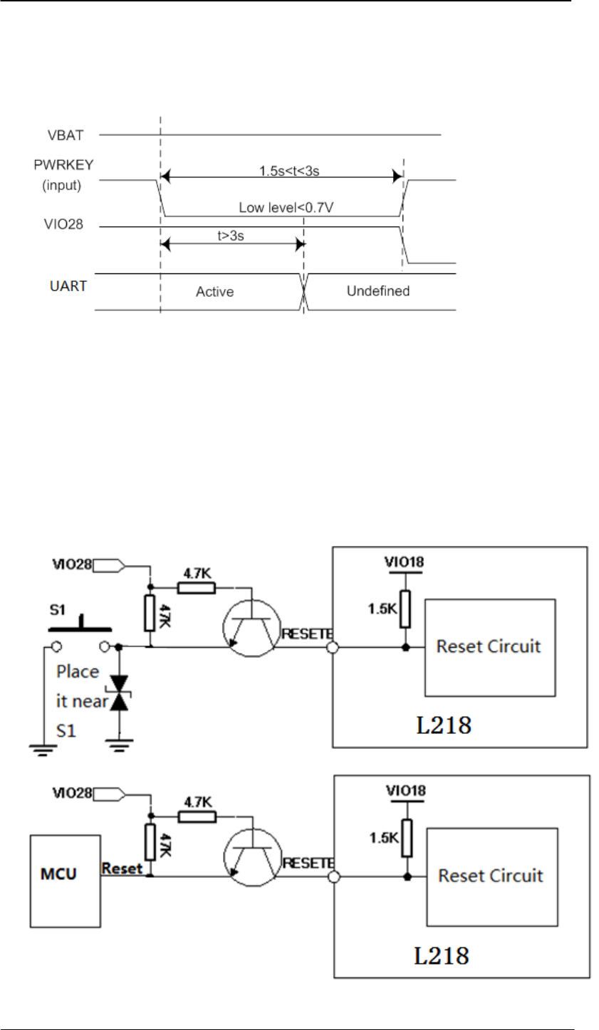
2、Use key boot
Figure 3-7: Use key to boot
Module on the mains electricity cannot be earlier than the external MCU with electricity, prevent
module on the electric moment, external MCU serial port is in unstable condition, cause the module
into the mode of the error. To ensure stable operation of external MCU, then control module is
powered on.
Boot sequence diagram below:
Figure 3-8: Boot sequence
Also pay attention to the external MCU and module connection interface level anomaly,
especially the main UART port, could affect the module of the boot sequence, when switched on. For
example, external MCU IO interface is in a state of output, the module of UART0 mouth U0RTS
signal (output pin) forced to lower or higher, the module may not be able to normal boot.
1
3.1.4 Power off
It is a safe way to turn off the module by driving the PWRKEY to a low level voltage for a
certain time. The power down scenario is illustrated below.
Figure 3-9 Shutdown sequence
Note: As logout network time is related to the local mobile network, it is recommended to delay
about 12 seconds before disconnecting the power supply or restarting the module.
3.1.5 Reset
The hardware reset reference design as below (Key reset and MCU reset L218 Module):
Figure 3-10: Recommend the reset circuit: Key reset and MCU reset L218 Module
1
Note:
1, Only use under emergency, such as no AT response, PWRKEY failure.
2, Don’t connect RESETB PIN to MCU directly.
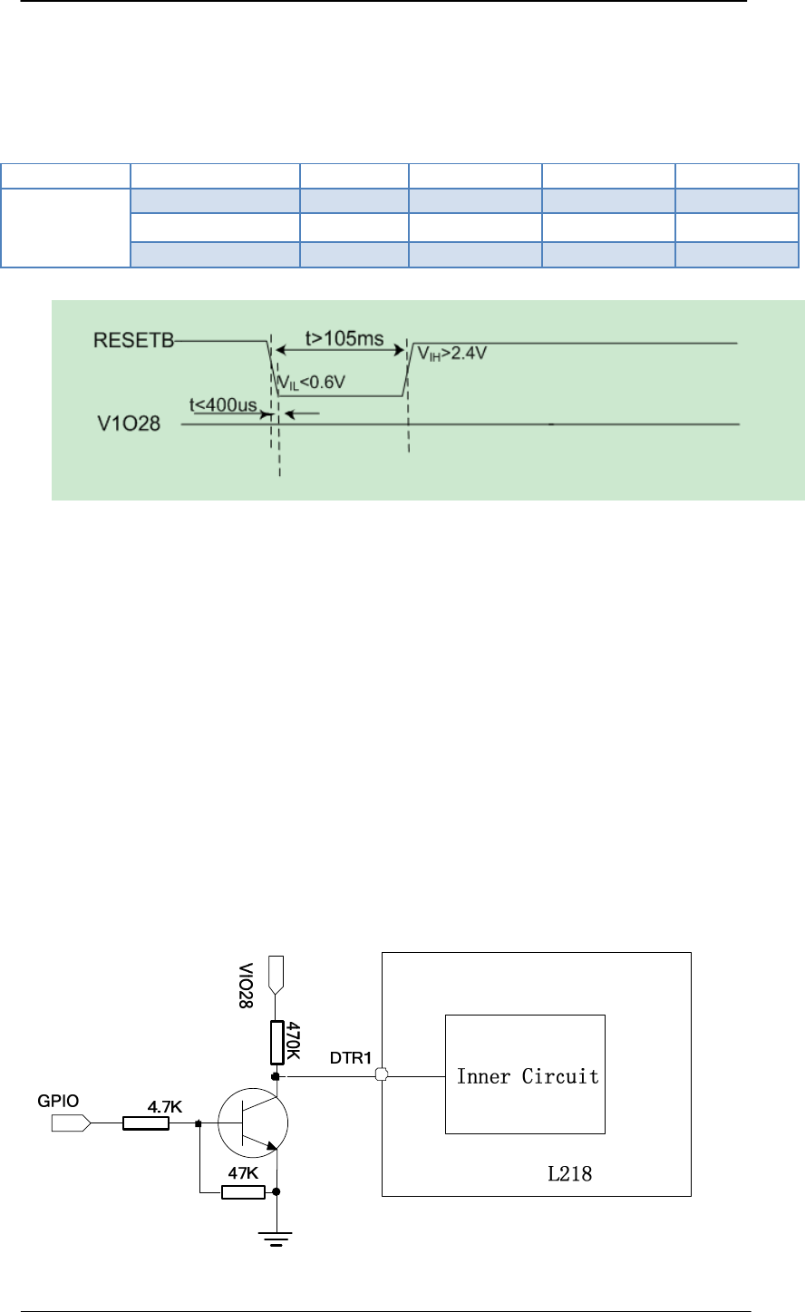
Table 5-2:Electronic characteristic of the RESET pin
PIN name Symbol Min Typ Max Unit
RESETB
VIH 2.4 -- -- V
VIL -- -- 0.6 V
Low power time 105 -- -- ms
RESETB Reset timing sequence:
Figure 3-11: Reset timing sequence
3.1.6 Power saving mode
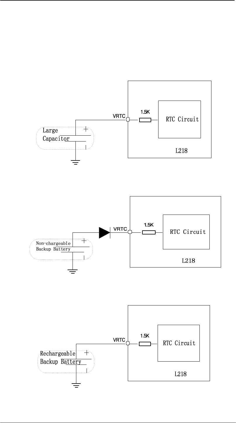
When L218 is in sleep mode, the following methods can wake up the module:
(1) Pull down DTR pin.
The serial port will be active after DTR pin is pulled to low level for about 50ms.
(2) Receive a voice or data call from network.
(3) Receive a SMS from network.
When L218 is in wake up mode, the following methods can sleep the module: Pull up DTR pin.
(1) Pull up DTR pin.
Figure 3-12:DTR circuit
1
3.1.7 RTC power
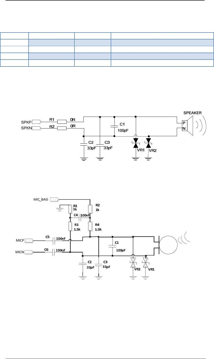
When VBAT disconnect, users need to save the real time clock, the VRTC pin can't hung up. It
need an external large capacitor or batteries. When external large capacitor, the recommended value
of 100uF, to keep the real time clock for 1 minute. RTC power using external large capacitor or
battery to RTC power supply inside the module. Modules contain a 1.5 K current-limiting resistance.
Button cell or super capacitor can be used to give the RTC power supply. Below are several to RTC
power supply circuit of reference:
External capacitor of power supply
Figure 3-13:External capacitor to the RTC power supply
Non-chargeable Backup battery
Figure 3-14:Non-rechargeable battery
Rechargeable battery
Figure 3-15:Rechargeable battery
The VRTC power typical value of 2.8 V, consumption flow about 3uA when VBAT disconnect.
2
3.2 Audio
Table 6-3:Audio interface pin definition
NO. PIN name PIN NO. Description
1 MICN 36 Audio differential input negative
2 MICP 37 Audio differential input positive
3 SPKN 34 Audio differential output negative
4 SPKP 35 Audio differential output positive
3.2.1 Audio channel
1、 The difference signal SPKN, SPKP of audio, directly connected to the speaker device.
Figure 3-16: Receiver circuit
2、 MIC need add external MICBIAS power, external microphone can be directly connected MICP
and MICN.
Figure 3-17: MIC (Reference circuit)

2
3.2.2 TDD noise
Electret microphone (with embedded double frequency filtering capacitor, 10pFand 47pF) is
suggested to use on hand handle or hand free microphone to stop RF interference and TDD noise
from the beginning. If double frequency filtering capacitor is not selected, TDD noise may be heard
during conversation. Please consult to capacitor provider to choose the most suitable capacitor value
to filter high-frequency noise out in GSM850/GSM900/DCS1800/PCS1900MHz.
The order of noise severity in GSM band depends on application design. For instance, TDD
noise is relatively serious in GSM900 or DCS1800 in different conditions. Users choose their desired
filter capacitor according to their situation. The place of nearing audio element or interface is better
for filter capacitor, wire layout must be shortest as it could be, through filter capacitor first. The place
far away from audio element or layout is better for antenna to avoid disturbing. Power layout and
audio layout cannot be paralled, and keep them in distance.
TDD noise can be affected by GND. If GND layout is not suitable, noise will disturb MIC and
speaker.
Add some large capacitors or series magnetic beads during schematic diagram designing to
avoid conductive interference.
Differential audio layout must abide the rules of differential signal layout.
3.3 UART Communication
3.3.1 Serial pin definition
Modules provide 2 groups of UART serial port, including UART1 support full serial port
function, main effect for the AT communications, data services, software upgrades, etc. UART2
provides only the TX and RX, can be used as the AT communication, debug, etc. Module called a
DCE device (Data Communication Equipment), according to the traditional DCE - DTE (Data
Terminal Equipment) connection. Adaptive baud rate support range 4800bps to 115200bps.
Table 7-4:Serial pin definition:
Interface PIN name PIN NO. Description
Serial port
DCD1 11 Data carrier detect
RTS1 8 DTE request data
RING1 7 Ringing indicating
DTR1 6 DTE is ready
CTS1 10 Clear to send
TXD1 4 Data sent
RXD1 5 Data reception
DSR1 9 Data Set Ready
3.3.2 Serial port characteristics
Main serial port:
7 signal lines. Including cable TXD and RXD, hardware flow control line RTS and
CTS, and other line of DTR, DCD and RI.
8 data bits,No parity,One stop bit.
Hardware flow control off by default, if use hardware flow control, use the "AT +
ICF = 0" open flow control function.
AT command transfer, GPRS data transmission.
Support a fixed baud rate is as follows:
2400,4800, 9600, 14400, 19200, 28800, 38400, 57600, 115200.
The default configuration module for adaptive baud rate. Adaptive support the
following baud rate:4800,9600,19200,38400,57600,115200bps.

2
The baud rate is fixed or adaptive baud rate synchronization settings. And send a command string
"A-T" when serial ready after module will reply "OK".
The host controller by sending "AT" command to the module, the module will automatically
detect and identify the host controller's current baud rate. Adaptive baud rate function can make the
host controller don't need to know the current baud rate and the module of communication will be
finished. Adaptive baud rate function open by default.
Adaptive baud rate operating configuration:
Serial interface is configured to 8 bits of data bits, parity bits, one stop bit (the
factory configuration).
Adaptive baud rate mode, if there is no first synchronization module boot, such as
"RDY", "+ CFUN: 1" and "+ CPIN: READY" URC information will not be reported.
DTE in switching to a new baud rate, will first through the "AT" set up the new baud
rate, before module detection and synchronous new baud rate, the module will use previous
messages URC baud rate. DTE when switch to the new baud rate, the equipment is likely to
receive unrecognized characters.
Baud rates, is not recommended in a fixed mode switch to the adaptive baud rate
model
Note: the default module is adaptive baud rate (AT + IPR = 0), in the baud rate adaptive mode,
after power on the URC information "RDY" will not back to the master machine. In the module boot
after 2 ~ 3 seconds, can send the module AT commands. Master need to first send the "AT" the baud
rate of character to the module to detect a master, and continue to send 1 ~ 5 "AT" string until module
returns "OK". Then send a "AT + IPR = x & W" command to the module set the baud rate of a fixed,
and save the configuration, after completed the configuration, each module after boot, will return to a
URC information via a serial port "RDY". To further understand, please refer to the document
[AT_DOCUMENT] "AT + IPR" in the chapter.
2
3.3.3 Serial port connection
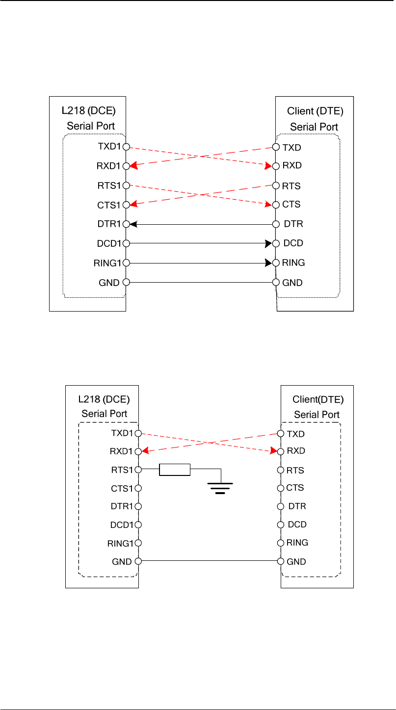
The main serial port connection mode is more flexible, as follows are three common ways of
connection.
1、Full-featured serial connection as shown in the figure below, this way is mainly used in the
modem mode dial (PPP)
Figure 3-18: Full-featured serial connection
2、Three wire system without hardware flow control of the serial port is as follows
Figure 3-19: Serial port three line connection
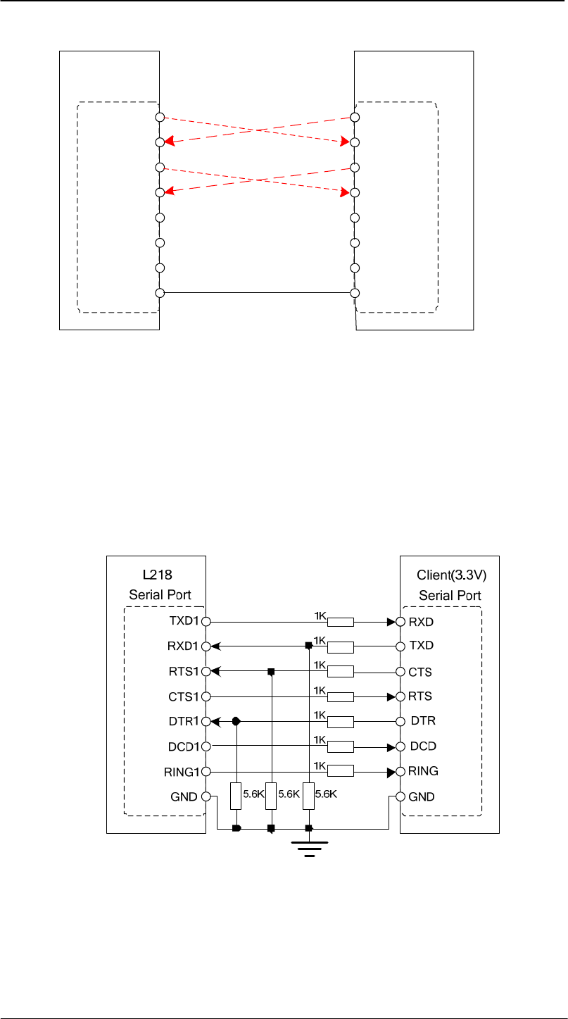
2
3、Three wire system with hardware flow control of the serial port is as follows:
TXD1
RXD1
RTS1
CTS1
DTR1
DCD1
RING1
TXD
RXD
RTS
CTS
DTR
DCD
RING
Serial Port Serial Port
L218 DCE Client(DET)
GND GND
Figure 3-20: Serial flow control connection
3.3.4 Serial level matching
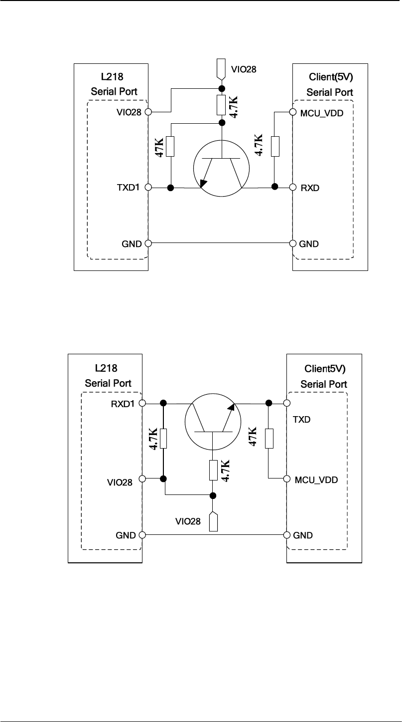
Module serial port is COMS VIO28 level signal, connected to the external MCU, it should pay
attention to the matching of IO level. Normal job requirements input level lower than 3.0V, the
default rate is 115200 bps.
When external MCU serial level of 3.3V, it is recommended to use the following reference
circuit. If the external MCU level is 3.0 V, please change the resistance of 5.6 K to 14 K.
Figure 3-21: Resistor level matching (Reference circuit)
2
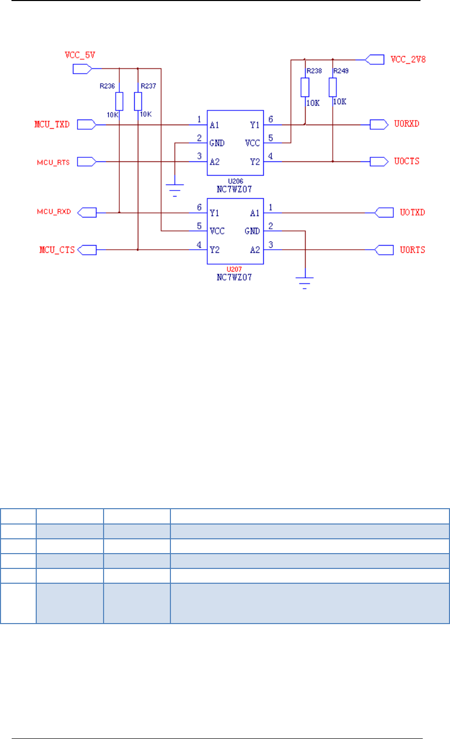
If the external host MCU serial level is 5V, can use the transistor voltage conversion circuit or
use special voltage conversion circuit, the reference is as follows:
1、 Use triode to do level transformation
Figure 3-22: 5V TXD level matching (Reference circuit)
Figure 3-23: 5V RXD level matching (Reference circuit)
2
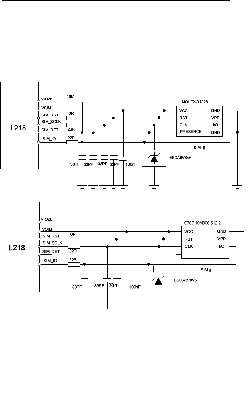
2、Use FAIRCHILD to convert the chip NC7WZ07:
Figure 3-24: Chip level matching (Reference circuit)
3.4 SIM Card Interface
SIM card interface support GSM Phase1 specification function, also support the function of the
GSM Phase 2 + specification and FAST 64 kbps SIM CARDS (for SIM application toolkit).
SIM card supports 1.8V and 3.0V power supply through the internal power supply of the module.
3.4.1 SIM Interface
Table 8-5:SIM card interface pin definition:
NO.PINnamePINNO.Description
1SIM_IO46SIMcarddataI/O
2SIM_SCLK47SIM cardcloc
k
3SIM_RST1SIM cardrese
t
4SIM_DET 3 SIM cardinsertdetectionpin
5VSIM2SIMpowersupply,accordingtothetypeofSIMcard
automaticallyselecttheoutputvoltage,3.0V10%or
1.8V10%,theoutputcurrentofabout10mA.
Below is a SIM card interface reference circuit, using 8 pin SIM gets stuck. SIM_DET pins for
Molex SIM booth detection. When cato is inserted into the booth, SIM_DET into a low level. At this
time whether or not a SIM card inside the cato, SIM_DET level from high to low make initialization
module produces a SIM card. By default, the SIM card detection is off, you can use the "AT + ESIMS
= 1" to open or "AT + ESIMS = 0" to close the function. Learn more about the content of the AT
command, please refer to the document [AT_DOCUMENT].
2
When sending the " AT+CPIN?" the order, if not SIM card into the booth, can appear the
URC information below:
+CPIN: NOT READY
If the SIM card has been done into the booth, SIM initialized, the URC information will
appear as below:
Call Ready
Figure 3-25: 8-pin SIM card (Reference circuit)
Figure 3-26: 6-pin SIM card (Reference circuit)
SIM card each signal need to increase the ESD protection devices used for ESD protection. In circuit
design, in order to ensure the good performance of SIM card and is not damaged, in circuit design
advice follow the following principles:
1. SIM gets stuck close to the module put, keep SIM card signal wiring less than 100 mm.
2. SIM card signal cable wiring away from the RF line and VBAT power line.
3. SIM gets-stuck and module of SIM_GND wiring to short and thick. SIM_VDD and SIM_GND
wiring width ensure that not less than 0.5 mm, and between SIM_VDD and GND bypass capacitor
does not exceed 1uf, and close to put SIM gets-stuck.
4. In order to prevent and SIM_DATA SIM_CLK signal crosstalk mutually, both wiring can't
stand too close to, and between two linear increase shielding. In addition, SIM_RST signal also need
to protect.
2
5. In order to ensure good ESD performance, it is recommended that the SIM card pin increase
TVS diode. Choose the TVS diode parasitic capacitor is not more than 50 pf, for example: WILL
ESDA6V8AV6 (http://www.willsemi.com).Series between the module and SIM card need to 22 ohm
resistance to suppress stray EMI and ESD protection. SIM card of peripheral devices should be
placed near the SIM holder.
6. Suggest SIM_DATA, SIM_RST SIM_CLK and SIM_VDD online parallel 33 pf capacitor is
used to filter out radio frequency interference, and close to put SIM gets-stuck.
3.4.2 SIM gets stuck (Reference Figure)
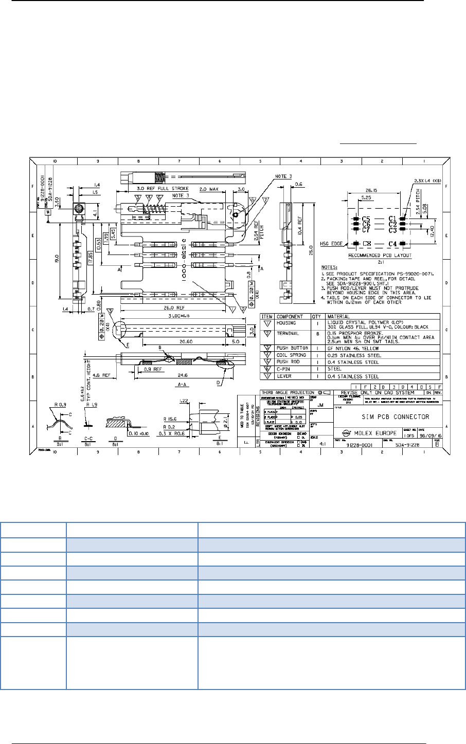
SIM card connector 8 pin recommended Molex 91228. Please visit the http://www.molex.com
website for more information!
Figure 3-27:Molex 91228 SIM gets stuck
Table 9-6:PIN description (Molex SIM gets stuck)
PINnameSignalDescription
C1 SIM_VDD SIM cardpowersupplypin
C2 SIM_RST SIM card reset
C3 SIM_CLK SIM card clock
C4 SIM_PRESENCE SIMcarddetectpin
C5 GNDGND
C6 VPP Not connected
C7 SIM_DATA SIM card data input/output
C8 SIM_DETECT
Card SIM in position detection, the pin is directly
connected to the ground, with the use of
SIM_PRESENCE. When the SIM card tray is inserted,
C4 and C8 are short circuit.
6 pins SIM booth is recommended to use Amphenol company C707 m006 10 5122.Please visit
http://www.amphenol.com for more information!
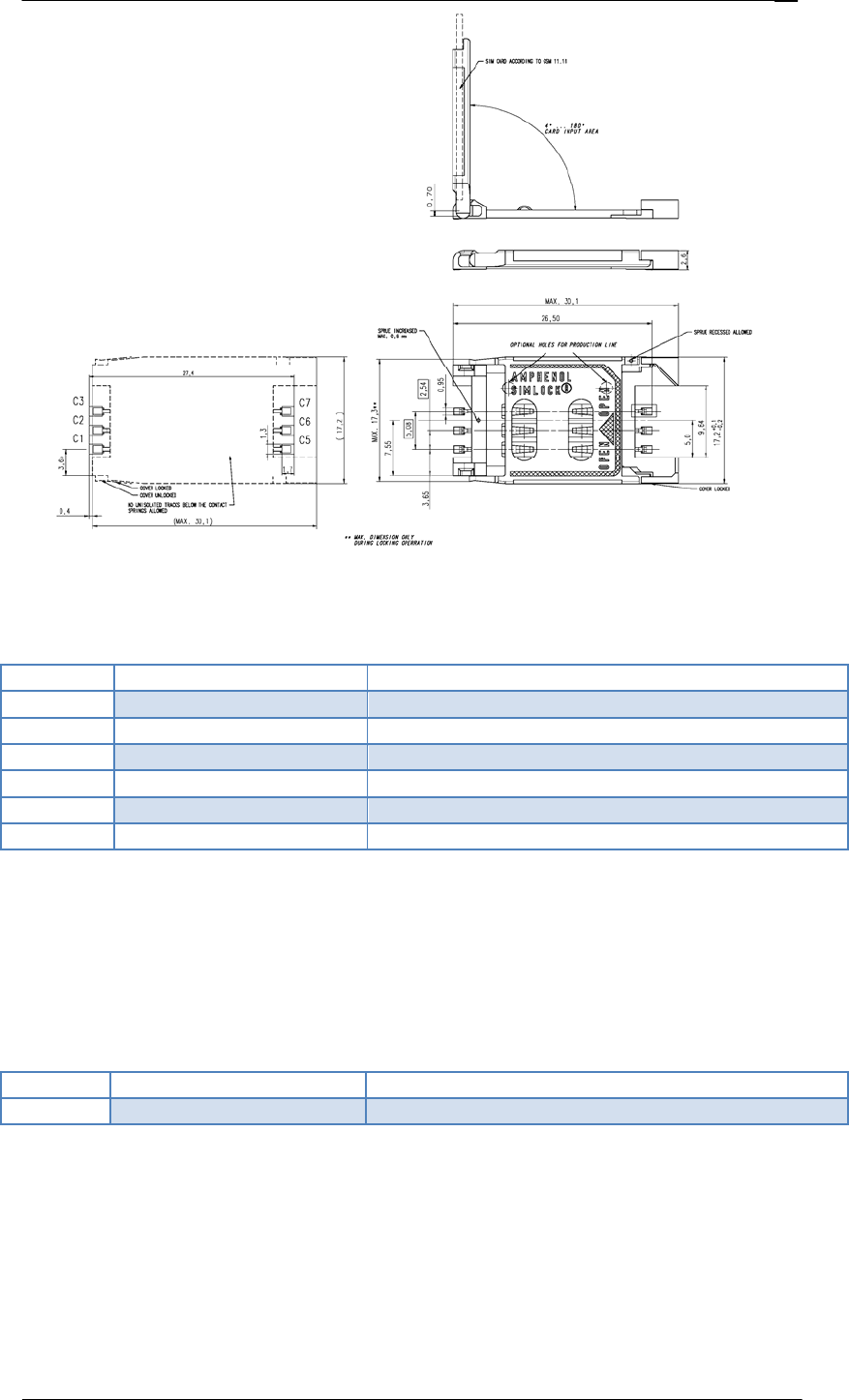
2
Figure 3-28:Amphenol C707 10M006 5122 SIM gets stuck
Table 10-7:PIN description (Amphenol SIM gets stuck)
PIN name Signal Description
C1 SIM_VDD SIM cardpowersupplypin
C2 SIM_RST SIM card reset
C3 SIM_CLK SIM card clock
C5 GND GND
C6 VPP Not connected
C7 SIM_DATA SIM card data input/output
3.5 PWM Interface
Table 11-8:PWM Pin definition
PIN NO. PIN name Description
14 PWM0 PWM signal, Reusable for GPIO2
PWM can provide the frequency range of 0~2KHz, the user can set the output frequency, duty
cycle through the AT+SPWM command, please refer to the AT document.
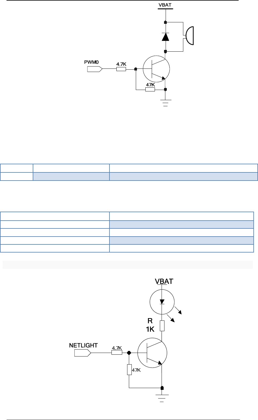
PWM pin can be used to drive buzzer.
NOTE: Make sure the PWM pin keep low level when module in the boot process.
Buzzer volume can be set by "AT + CRSL".
The reference circuit as follows:
3
Figure 3-29:PWM (Reference circuit)
3.6 NETWORK Status Indicator
Table 12-9:NETLIGHT pin definition
PIN NO. PIN name Description
29 NETLIGHT Network status indicator
The NETLIGHT signal can be used to drive network status LED, the working state of this pin in the
following table:
Table 13-10:working state of NETLIGHT
LightstatusWorkstatus
off Power off
64ms on/ 800ms off No Network
64ms on/ 3000ms off Register to network
64ms on/ 300ms off GPRS Data Communication
Reference circuit:
Figure 3-30:NETLIGHT (Reference circuit)

3
3.7 ADC Interface
L218 provides an ADC channel, the user can use the AT command "AT + CADC" to read voltage
value on ADC pin. Note: the ADC sampling the voltage cannot be more than 2.8 V, otherwise easy to
cause damage to the ADC. About the AT commands related information please refer to the document
[AT_DOCUMENT]. In order to improve the accuracy of ADC, the layout
of ADC should be surrounded by ground.
Table 14-11:ADC interface pin definition
PIN
NO. PIN name Description
30 ADC Analog sampling
Table 15-12:ADC Parameter
Item Min Typ. Max Units
Input voltage range 0 - 2.8 V
ADC resolution - 10 - bits
ADC sampling rate - - 1.0833 MHz
ADC precision 10 30 mV
3.8 GPS Function
L218 supports GPS, users only need external matching GPS antenna can be convenient to use
this feature.
Can use AT commands through the serial port to the GPS operation, in order to realize
positioning, and other functions.
3.9 Antenna Interface
L218 interface provides three antenna, GSM antenna interface RF_ANT respectively, and the
GPS antenna interface GPS_RF ANT_RF antenna and interface.
GPS antenna, GSM antenna, RF antenna working in choose all needs to choose frequency band
input impedance of 50 ohm, standing wave coefficient is less than 2 antenna products.
As far as possible away from two kinds of antenna is placed.
Each port antenna and other port isolation ratio should be greater than 30 dB.
3
L218 provides three antenna interfaces, pin definition as below:
Table 16-13:Antenna interface pin definition
PIN NO. PIN name Description
40 GPS-ANT GPS antenna interface
20 RF_ANT GSM antenna interface
17 RF-ANT RF antenna interface
3.9.1 GSM antenna reference circuit
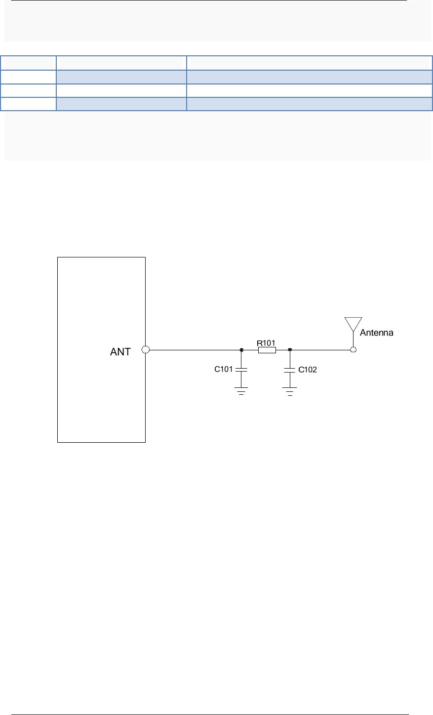
For the peripheral circuit design of the antenna interface, in order to better adjust the RF
performance, the proposed reservation matching circuit. Antenna connection reference circuit as
shown below. Where C101, C102 default is not posted, only 0 ohm R101 resistance, the line needs to
be controlled by 50 ohm.
Figure 3-31: RF reference circuit (GSM/BT)
Component placement and RF routing takes note:
Matching circuit must be placed near the antenna
RF ANT foot to the antenna RF cable must be 50 ohm impedance control
RF_ANT PIN to antenna RF line must be far away from the high speed signal lines and
strong interference sources, to avoid any signal lines cross or parallel and adjacent layer
3
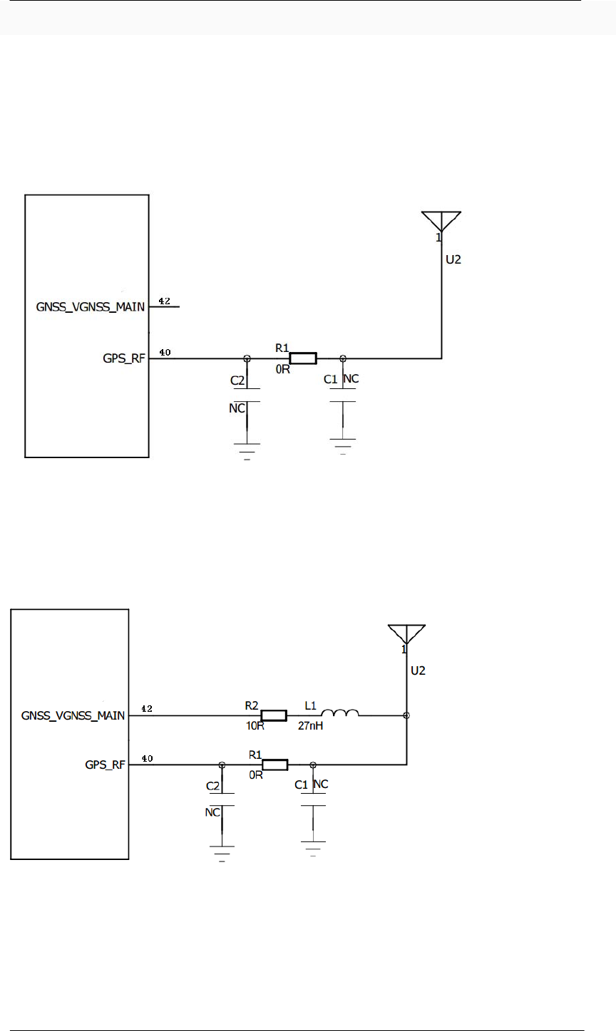
3.9.2 GPS antenna reference circuit
For the outside of the antenna interface circuit design, in order to better adjust the RF
performance, suggest the reserved matching circuit. GPS antenna can be divided into passive and
active antenna, the antenna connection reference circuit as shown in the figure below.
a. Passive antenna
Matching circuits of C1 and C2 default don't stick, Resistor R1 only 0 ohm, need to get the line
control according to 50 ohms.
Figure 3-32: GPS passive antenna (Reference circuit)
b. Active antenna
Active antenna is integrated with built-in LNA, need plus 2.8 V to 2.8 V, suggest 3.3 V power
supply. Matching circuits of C1 and C2 default don't stick, R1 resistor only 0 ohm, need to get the
line control according to 50 ohms.
Figure 3-33: GPS active antenna (Reference circuit)
Component placement and RF routing takes note:
Matching circuit must be placed near the antenna
RF _ANT foot to the antenna RF cable must be 50 ohm impedance control
RF_ANT PIN to antenna RF line must be far away from the high speed signal lines and
strong interference sources, to avoid any signal lines cross or parallel and adjacent layer
3
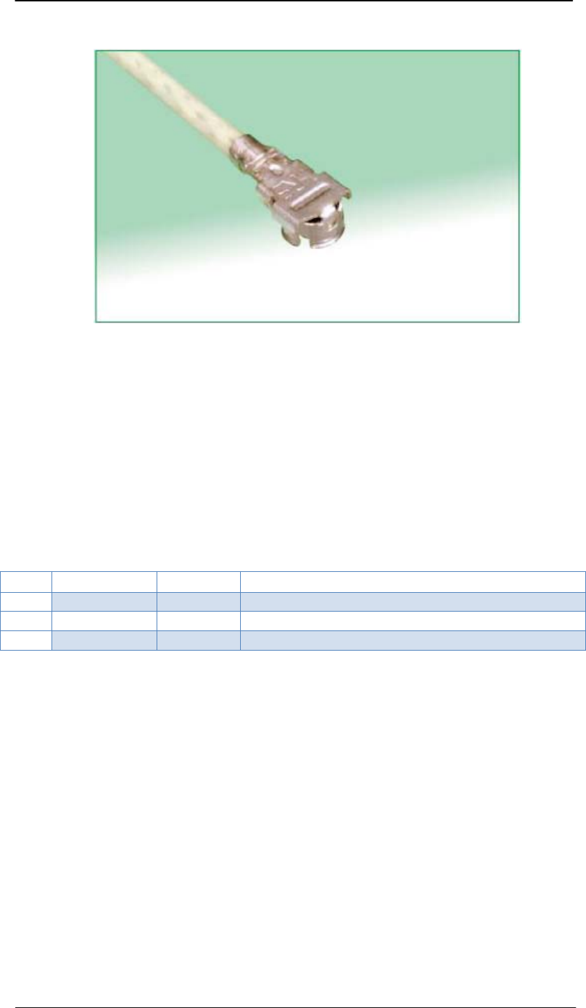
Gain and directivity Antenna directivity refers to the intensity of the electromagnetic field while the
electromagnetic wave is in all directions. Gain is the collection of the efficiency and directivity of the
antenna. It is recommended that antenna gain is less than or equal to 3dBi.
Figure 5-1 RF cable
3.10 USB Interface
3.10.1
Pin description
This product has a high speed USB1.1 interface, support full - speed mode, a main processor
(AP) and mainly through the USB interface for data transmission between modules. USB interface
are defined as follows.
Table 17-14:USB interface pin definition:
NO.PINname PINNO.Description
1VBUS_VBUS 43USBPower
2USB_DM44USBDifferentialdataD‐
3USB_DP45USBDifferentialdataD+
3.10.2 Electrical characteristics
The USB interface module accords with USB1.1 specification and electrical properties. Support
full - speed working mode. Main processor (AP) and the module of data between the interaction is
mainly completed through the USB interface.
3.10.3 USB interface applied
USB bus is mainly used for data transmission, software upgrades, detection module program.
Work under the mode of high - speed USB line, if you need to ESD design, must satisfy the junction
capacitor value of ESD protection devices < 5 pf, or larger junction capacitor will cause waveform
distortion, affect the bus communication. Differential difference of the data line impedance should be
controlled in 90 ohm + / - 10%.
3
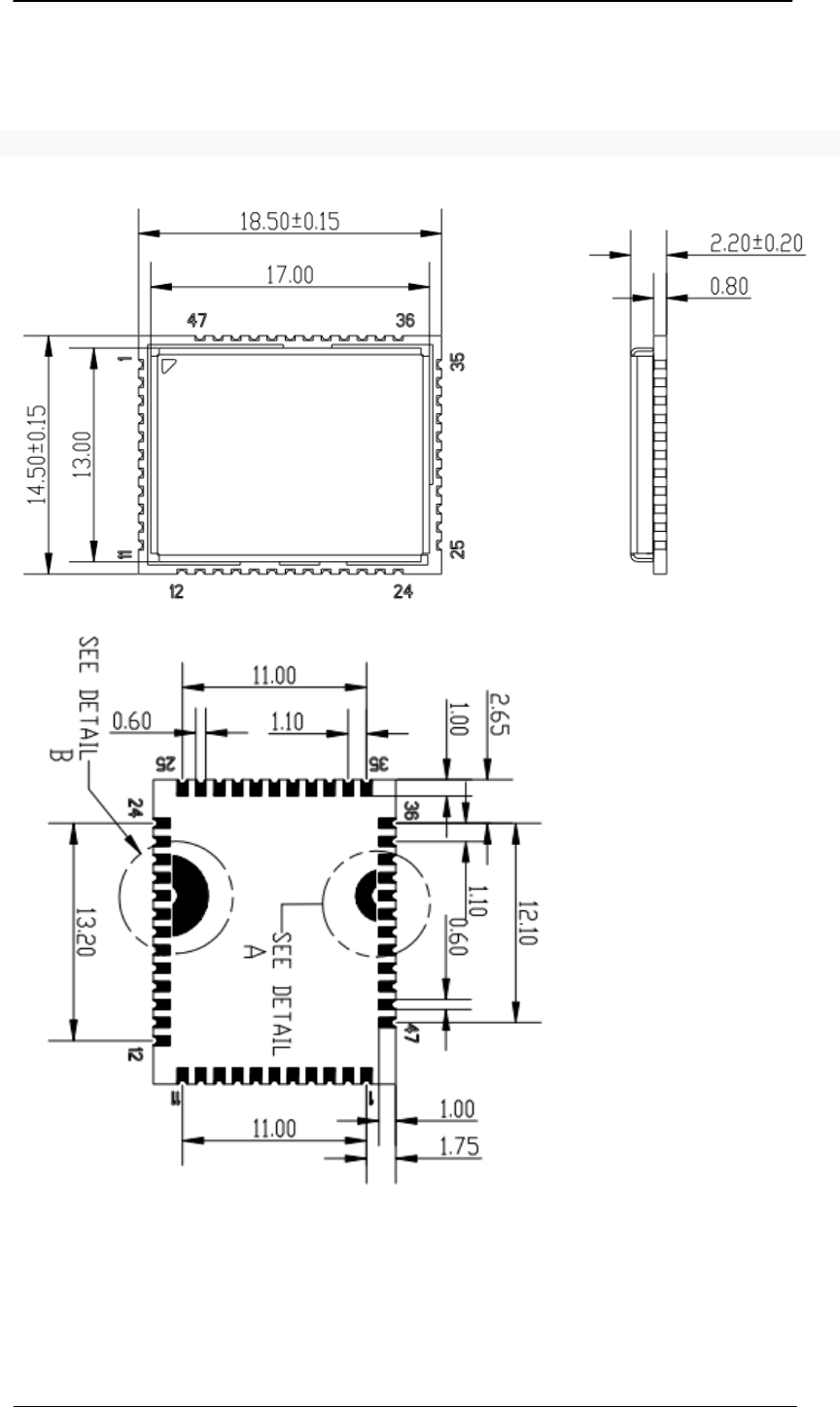
4 Mechanical Dimensions
Mechanical dimensions of Module:
Figure 4-1: L218 top view, side view, and bottom view(mm)
3
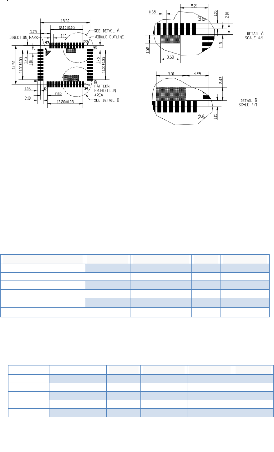
Figure 4-2: L218 Recommended Pad(mm)
5 ELECTRICAL CHARACTERISTICS
5.1 Absolute Maximum Ratings
The following table shows the absolute maximum state in abnormal situation, more than the
limit value will likely result in permanent damage to the module.
Table 5-1: Absolute Maximum Ratings
Parameter Min Typ. Max Unit
VBAT 3.3 3.6 4.4 V
Peak current -0.3 - 3 A
Digital signal input voltage -0.3 - 3.1 V
Analog input voltage -0.3 - 3.1 V
Working temperature -40 25 +85 ℃
Storage temperature -45 25 +90 ℃
5.2 Digital Interface Characteristics
Table 5-2: Digital Interface Characteristics
Parameter Description Min Typ. Max Unit
VIH Input high level 2.1 - 3.1 V
VIL Input high level 0 - 0.7 V
VOH Input high level 2.5 - 3.1 V
VOL Input high level 0 - 0.3 V
VIH Input high level 2.1 - 3.1 V
* Apply to the GPIO, I2C, UART, PCM digital interface, etc.

3
5.3 VSIM Characteristics
Table 5-3: SIM card interface characteristics
ParameterDescriptionMin Typ. Max Unit
VO Output voltage 1.65 1.8 1.95 V
2.8 3.0 3.2 V
IO Output current - - 60 mA
5.4 Current Consumption
Table 5-4: Current consumption
ParameterConditionsMin Typ. Max Unit
Bottom current Shutdown mode -- 0.07 -- mA
Working current
Sleep mode -- 2 -- mA
Standby mode -- 10.6 -- mA
Voice (maximum power) -- 280 -- mA
Data transfer mode
GPRS(1Rx,4Tx) -- 495 -- mA
Peak current
Data transfer mode
GPRS(3Rx,2Tx) -- 413 -- mA
Maximum power burst
current -- -- 2.0 A
Data transfer mode
GPRS(3Rx,2Tx) -- 413 -- mA
5.5 ESD
In the use of the module, due to the human body static electricity, electric charge and friction
between the two kinds of static electricity generated by various means of discharge to the module,
may cause some damage, so ESD protection must pay attention, whether in the development,
production assembly, testing process, especially in product design, should be taken to prevent ESD
protection measures. Such as circuit design in the interface or vulnerable to the ESD point to increase
the ESD protection, the production of anti-static gloves, etc.. Because the module is not specifically
designed for electrostatic discharge protection, so in the production, assembly and operation module
must pay attention to the electrostatic protection. The performance of the module test parameters in
the following table:
ESD performance parameters (temperature: 25, humidity: 45%)

3
Table 5-5: ESD performance parameters
PIN Contact discharge Air discharge
VBAT ±5KV ±10KV
GND ±5KV ±10KV
RXD, TXD ±1KV ±6KV
RF_ANT ±5KV ±10KV
MIC_P/N ±2KV ±6KV
RCV_P/N
PWRKEY ±3KV ±6KV
RESETB
5.6 RF performance
RF output power
Following table lists the conducted output power of modules, compliant with 3GPP TS 05.05 SPEC.
Table 5-6: GSM850 conducted output power
PCL Output power (dBm) Tolerance (dB) for conditions
-- Nominal Normal Extreme
5 32.5
±0.4 ±2
6 30.8 ±1 ±2
7 29
±1 ±2
8 27 ±1 ±2
9 25
±1 ±2
10 23 ±1 ±2
11 21
±1 ±2
12 19 ±1 ±2
13 17
±1 ±2
14 15 ±1 ±2
15 13
±1.5 ±2
16 11 ±1.5 ±2
17 9
±1.5 ±2
18 7 ±1.5 ±5
Table 5-7: PCS1900 conducted output power
PCL Output power (dBm) Tolerance (dB) for conditions
-- Nominal Normal Extreme
0 29.5 ±0.4 ±2
1 27.5 ±1 ±2
2 26 ±1 ±2
3 24 ±1 ±2
4 22 ±1 ±2
5 20 ±1 ±2
6 18 ±1 ±2

3
7 16 ±1 ±2
8 14 ±1 ±2
9 12 ±1.5 ±2
10 10 ±1.5 ±2
11 8 ±1.5 ±2
12 6 ±1.5 ±2
13 4 ±1.5 ±2
14 2 ±1.5 ±5
15 0 ±2 ±5
Module conduction receiver sensitivity
The following table lists the module's conduction reception sensitivity and is tested under static
conditions.
Table 5-8: Conduction sensitivity
Band Receiving sensitivity (Typ.)
GSM850 ≦-108dBm
PCS1900 ≦-108dBm
Module frequency band
The following table lists the module's working frequency bands, compliant with the TS 3GPP 5.05
specification.
Table 5-9: Module frequency band
Band Receiving sensitivity (Typ.) Receiving sensitivity (Max))
GSM850 869 ~ 894MHz 824 ~ 849MHz
PCS1800 1930 ~ 1990MHz 1850 ~ 1910MHz
4
6 MANUFACTURING
This chapter describes the related information.
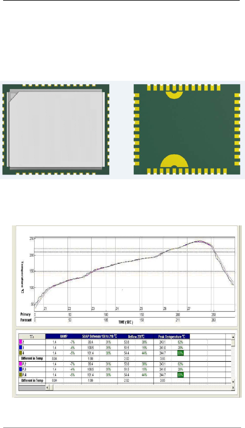
6.1 L218 Top And Bottom view
Figure 6-1: L218 top and bottom view
6.2 Soldering
Figure 6-2:Recommend reflow temperature profile

4
6.3 The Moisture Sensitivity Level (MSL)
L218 module complies with the humidity level 3. At a temperature of <30 degrees and relative
humidity of <60% of the environmental conditions, dry pack to perform J-STD-020C specification
according to IPC / JEDEC standard. At a temperature of < 40 degrees and a relative humidity of <
90% of the environmental conditions, in the case of unopened shelf life of at least six months. After
unpacking, Table29 shows the module shelf life at different times corresponding to the level of
humidity.
Table 6-1: Moisture sensitivity level and floor life
The Moisture Sensitivity Level
(MSL)
Floor Life(out of bag) at factory ambient≦ +30
/60%RH
1 RH ℃ condition
Unlimited at ≦ +30 /85%
2 1 Year
2a 4 weeks
3 168 hours
4 72 hours
5 48 hours
5a 24 hours
6 Mandatory bake before use. After bake, it must be reflowed
within the time limit specified on the label.
After unpacking, <30 degrees in temperature and relative humidity <60% environmental
conditions, 168 hours in the SMT patch. If not meet the above conditions need to be baked.
NOTES: For product handling, storage, processing, IPC / JEDEC J-STD-020C must be followed
6.4 Baking Requirements
Due to the humidity sensitive characteristics of the L218 module, the L218 is a vacuum
packaging, which can be stored for 6 months without damage to the package, and the ambient
temperature is less than 40 C and the relative humidity is less than 90%. To meet one of the following
conditions, the process of reflow soldering should be performed before the full bake, or the module
may cause permanent damage to the process.
1、Vacuum packing damage or leakage
2、The module is exposed in the air for 168 hours or more
3、The module is exposed in air for 168 hours, not meet the temperature <30 degrees and
relative humidity of the environment conditions <60%

4
Table 6-2: Baking requirements
Baking temperature Humidity Baking time
40°C±5°C <5% 192 Hours
120°C±5°C <5% 4 Hours
4
7. Package and Storage information
7.1 Package information
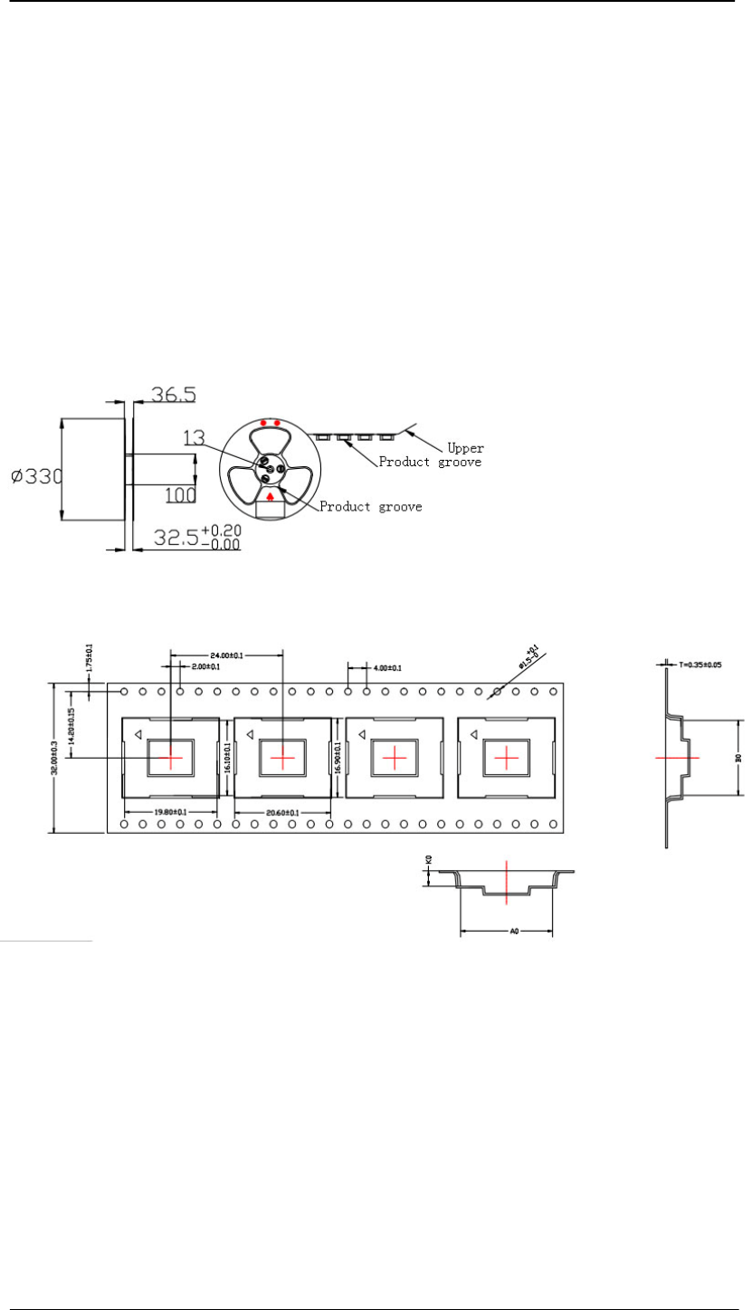
L218 module adopts by tape and reel. Shipping whit the coil packaging and vacuum sealing
anti-static bag to seal it.
7.1.1 Tape and reel information
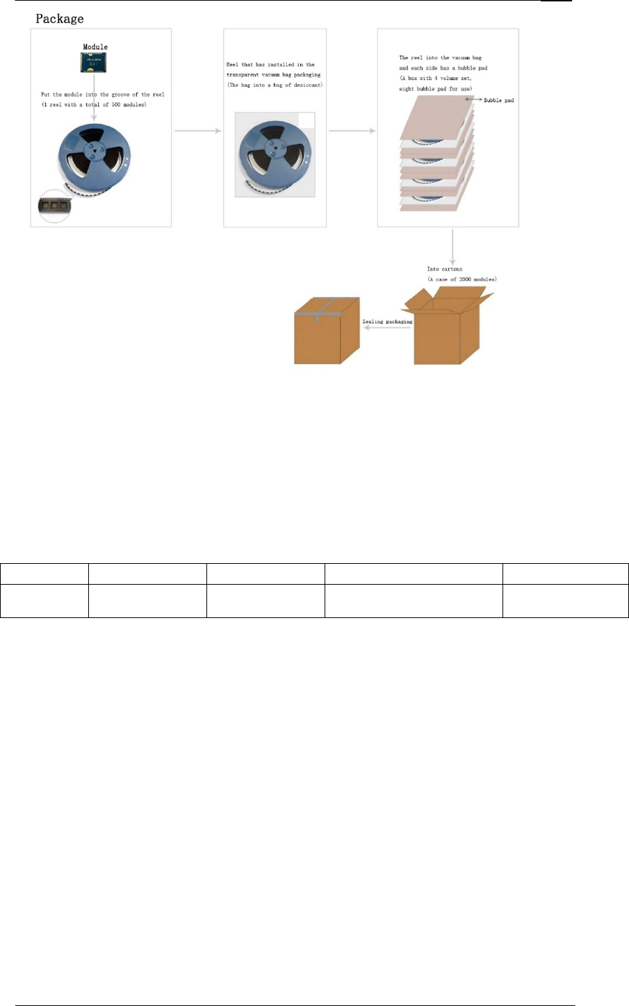
There are 500 L218 module assembled in a tape reel, below figure show the detail information.
Figure 7-1:Tape and reel information
7.1.2 Assemble and carrier information
L218 packing diagram is as follows, every 4 volumes of material packed in a case between each
volume of material has a bubble mat do isolation protection. Specific as shown in the figure below:
4
Figure 7-2:Package and ship information
7.2 Bagged storage conditions
L218 shipments in the form of vacuum sealing anti-static bag. Module of storage need to follow the
following conditions: Environment below 40 Degrees Celsius temperature, air humidity is less than
90% of cases, the module can be in vacuum sealed bags for 12 months. Conditions set the storage
environment Suggestions with reference to the following form.
Table 7-1: Storage conditions (less than 90% humidity of the air vacuum sealed packaging)
Parameter Min. Typ. Max. Unit
Storage
temperature
-45 25 90 ℃
When on the vacuum bags, if meet the following conditions, the module can be directly for reflow
soldering (furnace temperature setting reference 6.2 furnace temperature curve) or other high
temperature process:
Module temperature below 30 degrees c, the air humidity is less than 60%, factory within 72
hours to complete the SMT.
The humidity is less than 10%.
If the module is in the following conditions, to be baked before SMT:
When the environment temperature is 23 degrees Celsius (allow upper and lower volatility of 5
degrees Celsius), humidity index greater than 10%.
When open vacuum bags, module temperature below 30 degrees Celsius, air humidity is less
than 60%, but the factory have not finished the SMT within 72 hours.
When open the vacuum bags, module storage air humidity is more than 10%.
If modules need baking, please under 125 degrees Celsius (allowing fluctuations of 5 degrees Celsius)
up and down bake for 48 hours.

4
8 RELATED DOCUMENTS
Table 8-1:Related documents
NO. Documents Note
[1] AT_DOCUMENT
[2] ITU-T Draft new
recommendation V.25ter:Serial asynchronous automatic dialing and control
[3] GSM 07.07: Digital cellular telecommunications (Phase 2+); AT
command set for GSM Mobile Equipment (ME)
[4] GSM 07.10: Support GSM 07.10 multiplexing protocol
[5] GSM 07.05:
Digital cellular telecommunications (Phase 2+); Use
of Data Terminal Equipment – Data Circuit
terminating Equipment (DTE – DCE) interface for
Short Message Service (SMS) and Cell Broadcast
Service (CBS)
[6] GSM 11.14:
Digital cellular telecommunications system (Phase
2+); Specification of the SIM Application Toolkit for
the Subscriber Identity Module – Mobile Equipment
(SIM – ME) interface
[7] GSM 11.11: Digital cellular telecommunications system (Phase
2+); Specification of the Subscriber Identity Module
– Mobile Equipment (SIM – ME) interface

4
FCC Statement
NOTE: This equipment has been tested and found to comply with the limits for
a Class B digital device, pursuant to Part 15 of the FCC Rules. These limits are
designed to provide reasonable protection against harmful interference in a
residential installation. This equipment generates uses and can radiate radio
frequency energy and, if not installed and used in accordance with the
instructions, may cause harmful interference to radio communications.
However, there is no guarantee that interference will not occur in a particular
installation. If this equipment does cause harmful interference to radio or
television reception, which can be determined by turning the equipment off and
on, the user is encouraged to try to correct the interference by one or more of
the following measures:
---Reorient or relocate the receiving antenna.
---Increase the separation between the equipment and receiver.
---Connect the equipment into an outlet on a circuit different from that to which
the receiver is connected.
---Consult the dealer or an experienced radio/TV technician for help.
FCC Caution:
Changes or modifications not expressly approved by the party responsible for
compliance could void the user’s authority to operate the equipment.
IMPORTANT NOTE:
This module is intended for OEM integrator. The OEM integrator is still
responsible for the FCC compliance requirement of the end product, which
integrates this module. 20cm minimum distance has to be able to be
maintained between the antenna and the users for the host this module is
integrated into. Under such configuration, the FCC radiation exposure limits
set forth for an population/uncontrolled environment can be satisfied.
Any changes or modifications not expressly approved by the manufacturer
could void the user’s authority to operate this equipment.
FCC Radiation Exposure Statement
This equipment complies with FCC radiation exposure limits set forth for an
uncontrolled environment. This equipment should be installed and operated
minimum distance 20cm between the radiator and your body as well as kept
minimum 20cm from radio antenna depending on the Mobile status of this
module usage. This module should NOT be installed and operating
simultaneously with other radio. The manual of the host system, which uses
L218, must include RF exposure warning statement to advice user should keep
minimum 20cm from the radio antenna of L218module depending on the
status.

LABEL OF THE END PRODUCT:
The final end product must be labelled in a visible area with the following
"Contains TX FCC ID: 2AHSAL218". If the size of the end product is smaller
than 8x10cm, then additional FCC part 15.19 statement is required to be
available in the users manual: This device complies with Part 15 of the FCC
Rules. Operation is subject to the following two conditions: (1) this device may
not cause harmful interference, and (2) this device must accept any
interference received, including interference that may cause undesired
operation.
USERS MANUAL OF THE END PRODUCT:
In the users manual of the end product, the end user has to be informed to
keep at least 20cm separation with the antenna while this end product is
installed and operated. The end user has to be informed that
the FCC radio-frequency exposure guidelines for an uncontrolled
environment can be satisfied. The end user has to also be informed that any
changes or modifications not expressly approved by the
manufacturer could void the user’s authority to operate this equipment. If
the size of the end product is smaller than 8x10cm, the additional FCC part
15.19 statement is required to be available in the users manual: This device
complies with Part 15 of FCC rules. Operation is subject to the following two
conditions: (1) this device may not cause harmful interference, and (2) this
device must accept any interference received, including interference that may
cause undesired operation.
EU Regulatory Conformance
Hereby, we (Shanghai MobileTek Communication Ltd.) declared that this
device is in compliance with the essential requirements and other relevant
provisions of Directive 1999/5/EC.
The module is only certified with the installed antenna. Any change of the
antenna will void the certification. The host device including this RF
module need to undergo separate certification.
This module is intended for OEM integrator only and the OEM integrators
and instructed to ensure that the end user has no manual instructions to
remove or install the device. The OEM integrator is still responsible for
the FCC compliance requirement of the end product, which integrates this
module.