Montage Technology M88WI6000SIP M88WI6000 WiFi Module User Manual MWI042A Module

Montage Technology (Taiwan) Co., Ltd. M88WI6000 WiFi Module MWI042A Module

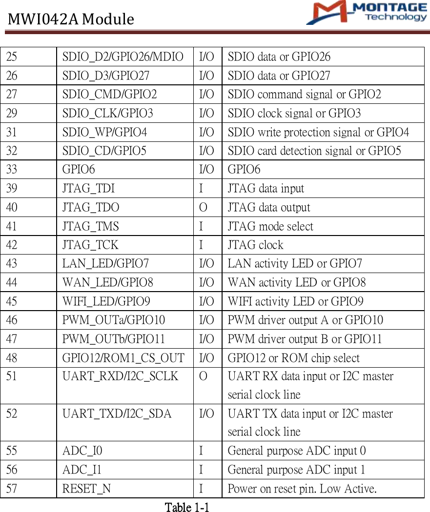
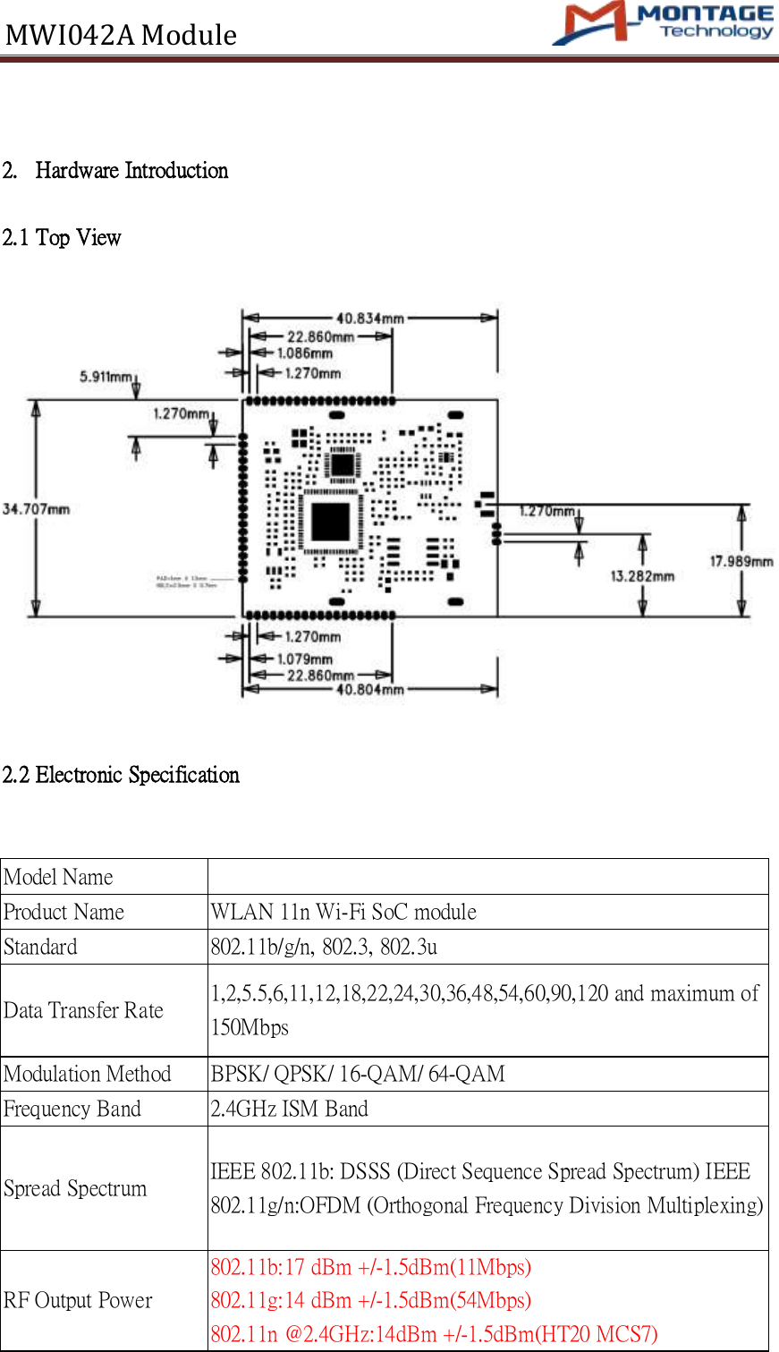
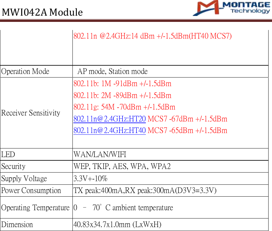
Module Specification

MWI042A Module                                            M88WI6xxx Wi-Fi SoC module Version: MWI042A Date: 2015/3/2
MWI042A Module                                            1.1 Introduction     The M88WI6xxx is a stand-alone SoC Wi-Fi module providing fully integrated 2.4GHz 802.11 b/g/n radio.It also provides flexible peripheral interfaces such as USB2.0,Ethernet PHY,PCM,RMII Interface,SDIO,JTAG,PWM,UART,I2C,ADC, GPIO to connect various peripheral interfaces directly to the M88WI6xxx Wi-Fi module. 1.2 Block Diagram      M88WI6032D/     M88WI6008S802.11n1T1RMACBB802.11n1T1R2.4GHzRFEthernet PHY Interface JTAGUSB 2.0PCMLED(WAN/LAN/WiFi)SDIORMII InterfaceInterfacePWMUARTI2CADCGPIO 1.3 Features *power supply +3.3VDC *USB 2.0 Host   *Ethernet PHY Interface   *PCM *RMII Interface *SDIO *JTAG *LED x3(LAN/WAN/WIFI) *PWM *UART *I2C *ADC
MWI042A Module                                            *GPIO *1x1 modes. *150Mhz PHY Rate Support. *20Mhz/40Mhz channel bandwidth. *Multiple BSSID *QoS-WMM,WMM Power Save 1.4 Pin Description Table 1-1 shows a detailed pin functional description of module MWI042A.  Figure 1-1 MWI042A Pin Assignment Diagram
MWI042A Module                                              Type Description I Input pin O Output pin I/O Bidirectional input/output P Power  Pin No. Label Type Description 1 SYSTEM_CLK_40M O Clock output pin for 40Mhz. 2,5,8,16, 17,21,28, 30,37,38, 50,53,54 DGND P These pins should be connected to ground plane. 3 USB_DM I/O USB    data   pin   Data‐ 4 USB_DP I/O USB    data   pin   Data+ 6 EPHY_RX_IN I Ethernet PHY RX differential input 7 EPHY_RX_IP I Ethernet PHY RX differential input 9 EPHY_TX_ON O Ethernet PHY TX differential output 10 EPHY_TX_OP O Ethernet PHY TX differential output 11 GPIO14/PCM0_TXD/ P1_CRSDV_EXT I/O GPIO14 or PCM data output signal or RMII CRSDV 12 GPIO15/PCM0_RXD/ P1_RXD_EXT0 I/O GPIO15 or PCM data input signal or RMII RXD0 13 GPIO16/PCM0_FS/ P1_RXD_EXT1 I/O GPIO16 or PCM frame sync signal or RMII RXD1 14 GPIO17/PCM0_BCLK/ P1_RMII_CLK_EXT I/O GPIO17 or PCM bit clock signal or RMII Clock 15 GPIO18/PCM0_MCLK/ P1_TXEN_EXT I/O GPIO18 or PCM master clock signal Or RMII TXEN 18,19,22,34,35,36,49 D3V3 P Digital 3.3 V power supply 20 VDD_REGSDIO P Regulator output for SDIO card 23 SDIO_D0/GPIO24 I/O SDIO data or GPIO24 24 SDIO_D1/GPIO25/MDC I/O SDIO data or GPIO25
MWI042A Module                                            25 SDIO_D2/GPIO26/MDIO I/O SDIO data or GPIO26 26 SDIO_D3/GPIO27 I/O SDIO data or GPIO27 27 SDIO_CMD/GPIO2 I/O SDIO command signal or GPIO2 29 SDIO_CLK/GPIO3 I/O SDIO clock signal or GPIO3 31 SDIO_WP/GPIO4 I/O SDIO write protection signal or GPIO4 32 SDIO_CD/GPIO5 I/O SDIO card detection signal or GPIO5 33 GPIO6 I/O GPIO6 39 JTAG_TDI I JTAG data input 40 JTAG_TDO O JTAG data output 41 JTAG_TMS I JTAG mode select 42 JTAG_TCK I JTAG clock 43 LAN_LED/GPIO7 I/O LAN activity LED or GPIO7 44 WAN_LED/GPIO8 I/O WAN activity LED or GPIO8 45 WIFI_LED/GPIO9 I/O WIFI activity LED or GPIO9 46 PWM_OUTa/GPIO10 I/O PWM driver output A or GPIO10 47 PWM_OUTb/GPIO11 I/O PWM driver output B or GPIO11 48 GPIO12/ROM1_CS_OUT I/O GPIO12 or ROM chip select 51 UART_RXD/I2C_SCLK O UART RX data input or I2C master serial clock line 52 UART_TXD/I2C_SDA I/O UART TX data input or I2C master serial clock line 55 ADC_I0 I General purpose ADC input 0 56 ADC_I1 I General purpose ADC input 1 57 RESET_N I Power on reset pin. Low Active. Table 1-1
MWI042A Module                                              2. Hardware Introduction  2.1 Top View    2.2 Electronic Specification   Model Name      Product Name   WLAN 11n Wi-Fi SoC module   Standard   802.11b/g/n, 802.3, 802.3u   Data Transfer Rate   1,2,5.5,6,11,12,18,22,24,30,36,48,54,60,90,120 and maximum of 150Mbps   Modulation Method   BPSK/ QPSK/ 16-QAM/ 64-QAM   Frequency Band   2.4GHz ISM Band   Spread Spectrum   IEEE 802.11b: DSSS (Direct Sequence Spread Spectrum) IEEE 802.11g/n:OFDM (Orthogonal Frequency Division Multiplexing)   RF Output Power   802.11b:17 dBm +/-1.5dBm(11Mbps) 802.11g:14 dBm +/-1.5dBm(54Mbps) 802.11n @2.4GHz:14dBm +/-1.5dBm(HT20 MCS7)
MWI042A Module                                            802.11n @2.4GHz:14 dBm +/-1.5dBm(HT40 MCS7)   Operation Mode     AP mode, Station mode Receiver Sensitivity   802.11b: 1M -91dBm +/-1.5dBm 802.11b: 2M -89dBm +/-1.5dBm 802.11g: 54M -70dBm +/-1.5dBm 802.11n@2.4GHz:HT20 MCS7 -67dBm +/-1.5dBm 802.11n@2.4GHz:HT40 MCS7 -65dBm +/-1.5dBm  LED   WAN/LAN/WIFI Security   WEP, TKIP, AES, WPA, WPA2   Supply Voltage 3.3V+-10% Power Consumption   TX peak:400mA,RX peak:300mA(D3V3=3.3V) Operating Temperature 0  –  70°  C ambient temperature   Dimension   40.83x34.7x1.0mm (LxWxH)
MWI042A Module                                            Federal Communications Commission (FCC) Statement  15.21 You are cautioned that changes or modifications not expressly approved by the part responsible for compliance could void the user’s authority to operate the equipment.  15.105(b) This equipment has been tested and found to comply with the limits for a Class B digital device, pursuant to part 15 of the FCC rules. These limits are designed to provide reasonable protection against harmful interference in a residential installation. This equipment generates, uses and can radiate radio frequency energy and, if not installed and used in accordance with the instructions, may cause harmful interference to radio communications. However, there is no guarantee that interference will not occur in a particular installation. If this equipment does cause harmful interference to radio or television reception, which can be determined by turning the equipment off and on, the user is encouraged to try to correct the interference by one or more of the following measures:  -Reorient or relocate the receiving antenna. -Increase the separation between the equipment and receiver. -Connect the equipment into an outlet on a circuit different from that to which the receiver is connected. -Consult the dealer or an experienced radio/TV technician for help.  This device complies with Part 15 of the FCC Rules.Operation is subject to the following two conditions: 1) this device may not cause harmful interference and 2) this device must accept any interference received, including interference that may cause undesired operation of the device.  RF Radiation Exposure Statement: This equipment complies with FCC RF radiation exposure limits set forth for an uncontrolled environment. This equipment should be installed and operated with a minimum distance of 20 centimeters between the radiator and your body. This Transmitter must not be co-located or operating in conjunction with any other antenna or transmitter.
MWI042A Module                                            Only those antennas with same type and lesser gain filed under this FCC ID number can be used with this device. The final system integrator must ensure there is no instruction provided in the user manual or customer documentation indicating how to install or remove the transmitter module.  Required end product labeling: Any device incorporating this module must include an external, visible, permanent marking or label which states: “Contains FCC ID: 2AEDFM88WI6000SIP

Navigation menu