Montage Technology WM6800K M88WI6800-K Wi-Fi Module User Manual
Montage Technology (Taiwan) Co., Ltd. M88WI6800-K Wi-Fi Module
UserManual.wiki
>
Montage Technology
>
WM6800K User Manual
User Manual
Navigation menu
Upload a User Manual
Namespaces
Wiki Guide
HTML
PDF
Info
Views
User Manual
Discussion / Help
Navigation
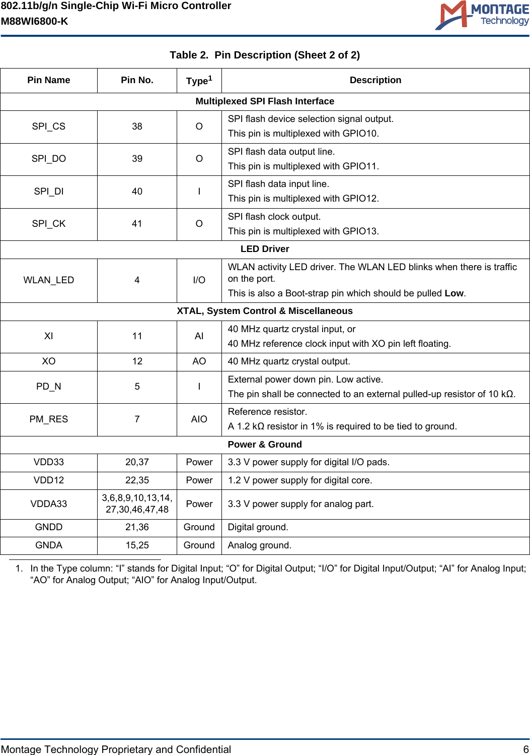
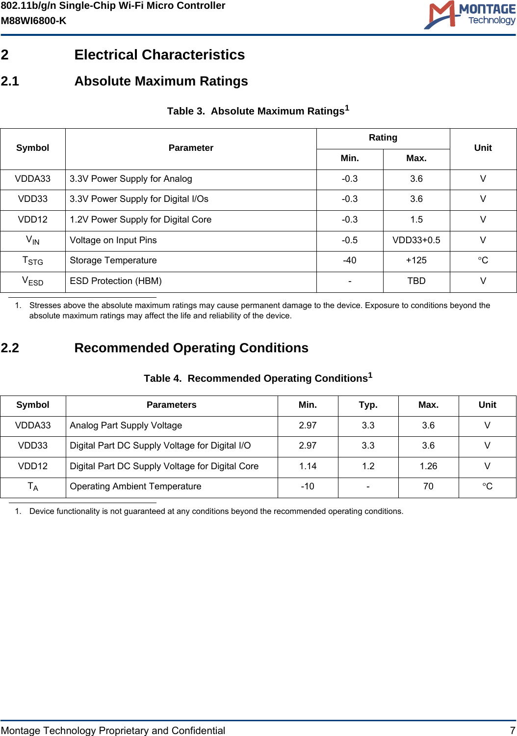
![802.11b/g/n Single-Chip Wi-Fi Micro ControllerM88WI6800-KMontage Technology Proprietary and Confidential 51.3 Pin DescriptionTable 2. Pin Description (Sheet 1 of 2)Pin Name Pin No. Type1DescriptionRF Transceiver InterfaceRF_TR_P 1 RF Differentia RF input/output (plus), or Single-ended RF input/output.RF_TR_N 2 RF Differentia RF input/output (minus), or GNDA for Single-ended mode.DCDC Converter InterfaceBUCK_LX 26 AO Analog output of DCDC converter.ADC Input InterfaceADC_IN1 28 AI Analog input 1 of ADC.ADC_IN0 29 AI Analog input 0 of ADC.GPIOsGPIO[3:0] 19,18,17,16 I/O General purpose input/output pins.GPIO[5:4] 24,23 I/O General purpose input/output pins.GPIO[9:6] 34,33,32,31 I/O General purpose input/output pins.GPIO10 38 I/O General purpose input/output pin.This is also a Boot-strap pin which should be pulled High.GPIO11 39 I/O General purpose input/output pin.This is also a Boot-strap pin which should be pulled Low.GPIO12 40 I/O General purpose input/output pin.GPIO13 41 I/O General purpose input/output pin.This is also a Boot-strap pin which should be pulled Low.GPIO[18:16] & GPIO14 45,44,43,42 I/O General purpose input/output pins.Multiplexed UART InterfacesUART0_RXD 17 I UART receive pin.This pin is multiplexed with GPIO1.UART0_TXD 16 O UART transmit pin.This pin is multiplexed with GPIO0.UART1_RXD 32 IUART receive pin. This pin is multiplexed with GPIO7. It shall be connected to an external pulled-up resistor of 10 kΩ.UART1_TXD 31 O UART transmit pin.This pin is multiplexed with GPIO6.Multiplexed PWM DriversPWM[3:0] 34,33,32,31 O PWM driver outputs. These pins are multiplexed with GPIO[9:6].](https://usermanual.wiki/Montage-Technology/WM6800K/User-Guide-3503146-Page-12.png)