Montage Technology WM6800K M88WI6800-K Wi-Fi Module User Manual
Montage Technology (Taiwan) Co., Ltd. M88WI6800-K Wi-Fi Module
User Manual

Montage Technology Proprietary and Confidential
802.11b/g/n Single-Chip Wi-Fi
Micro Controller
M88WI6800-K
Data Sheet
Revision Number: 0.1
Revision Date: Nov. 17, 2016

Disclaimer
INFORMATION IN THIS DOCUMENT IS PROVIDED IN CONNECTION WITH MONTAGE PRODUCTS. NO
LICENSE, EXPRESS OR IMPLIED, BY ESTOPPEL OR OTHERWISE, TO ANY INTELLECTUAL PROPERTY
RIGHTS IS GRANTED BY THIS DOCUMENT. EXCEPT AS PROVIDED IN MONTAGE'S TERMS AND
CONDITIONS OF SALE FOR SUCH PRODUCTS, MONTAGE ASSUMES NO LIABILITY WHATSOEVER, AND
MONTAGE DISCLAIMS ANY EXPRESS OR IMPLIED WARRANTY, RELATING TO SALE AND/OR USE OF
MONTAGE PRODUCTS INCLUDING LIABILITY OR WARRANTIES RELATING TO FITNESS FOR A
PARTICULAR PURPOSE, MERCHANTABILITY, OR INFRINGEMENT OF ANY PATENT, COPYRIGHT OR
OTHER INTELLECTUAL PROPERTY RIGHT.
Montage may make changes to specifications and product descriptions at any time, without notice.
Designers must not rely on the absence or characteristics of any features or instructions marked "reserved" or
"undefined." Montage reserves these for future definition and shall have no responsibility whatsoever for conflicts
or incompatibilities arising from future changes to them.
Other names and brands may be claimed as the property of others.
Do not disclose or distribute to any third party without written permission of Montage.
Copyright © Montage Technology Group Limited and/or its affiliated companies. All rights reserved.
802.11b/g/n Single-Chip Wi-Fi Micro Controller
M88WI6800-K
Montage Technology Proprietary and Confidential
802.11b/g/n Single-Chip Wi-Fi Micro Controller
M88WI6800-K
Montage Technology Proprietary and Confidential iii
Preface
This data sheet is the primary reference for the 802.11b/g/n Single-Chip Wi-Fi Micro Controller - M88WI6800-K. It
includes complete pin information, functional description, register description and electrical specifications for
engineers who may evaluate or use the device.
Conventions
The following conventions are used in this data sheet for easy and effective explanation.
•Cross-references are highlighted in blue for your attention. You can click on them to jump to the target pages.
•Number representation
−A hexadecimal number is represented by xxxxH or n’hxxxx (h/H: hexadecimal; n: number of bits).
−A binary number is represented by xxxxB or n’bxxxx (b/B: binary; n: the number of bits). Sometimes the
binary number with only one bit is also represented by ‘0’ or ‘1’.
−Other numbers should be considered as decimal numbers unless otherwise stated.
Terms and Abbreviations
Term Definition Term Definition
ADC Analog to Digital Converter PHY Physical layer device
AGC Automatic Gain Control QoS Quality of Service
AMPDU Aggregated MAC Protocol Data Unit RF Radio Frequency
AP Access Point SDR Single Data Rate
BBP Baseband Processor SNAP Subnetwork Access Protocol
BOM Bill of Material SPI Serial Programming Interface
DDR Dual Data Rate TR Transmit / Receive (T/R)
LAN Local Area Network UART Universal Asynchronous Receiver/Transmitter
LLC Logical Link Control UDP User Datagram Protocol
MAC Media Access Controller WAPI WLAN Authentication and Privacy Infrastructure
MIC Message Integrity Check WEP Wireless Encryption Protocol
MSDU MAC Service Data Unit WLAN Wireless Local Area Network
NAT Network Address Translation WMM Wi-Fi Multimedia
NVRAM Non-Volatile Random Access Memory WMM-PS WMM-Power Save
OS Operating System WPA Wi-Fi Protected Access
PA Power Amplifier WPS Wi-Fi Protected Setup

802.11b/g/n Single-Chip Wi-Fi Micro Controller
M88WI6800-K
Montage Technology Proprietary and Confidential iv
Revision History
Revision
Number Revision Date Changes
Page Number Description
0.1 Nov. 17, 2016 - Change Part Number from M88WI8000 to M88WI6800-K.
0.0 July 15, 2016 - Initial Release

802.11b/g/n Single-Chip Wi-Fi Micro Controller
M88WI6800-K
Montage Technology Proprietary and Confidential v
Table of Contents
Preface................................................................................................................................................................... iii
Features.................................................................................................................................................................. 1
Applications ........................................................................................................................................................... 1
General Description............................................................................................................................................... 1
Functional Block Diagram..................................................................................................................................... 2
1 Pin Information............................................................................................................................................... 3
1.1 Pin Assignment ....................................................................................................................................... 3
1.2 Pin List .................................................................................................................................................... 4
1.3 Pin Description........................................................................................................................................ 5
2 Electrical Characteristics .............................................................................................................................. 7
2.1 Absolute Maximum Ratings .................................................................................................................... 7
2.2 Recommended Operating Conditions..................................................................................................... 7
2.3 DC Electrical Characteristics .................................................................................................................. 8
2.4 Current Consumption.............................................................................................................................. 8
3 Mechanical Package Data.............................................................................................................................. 9

802.11b/g/n Single-Chip Wi-Fi Micro Controller
M88WI6800-K
Montage Technology Proprietary and Confidential vi
List of Figures
Figure 1. Functional Block Diagram for M88WI6800-K ...................................................................................... 2
Figure 2. QFN48 Pin Assignment....................................................................................................................... 3
Figure 3. QFN48 Package Outline ..................................................................................................................... 9

802.11b/g/n Single-Chip Wi-Fi Micro Controller
M88WI6800-K
Montage Technology Proprietary and Confidential vii
List of Tables
Table 1. Signals By Pin Number ....................................................................................................................... 4
Table 2. Pin Description .................................................................................................................................... 5
Table 3. Absolute Maximum Ratings................................................................................................................. 7
Table 4. Recommended Operating Conditions ................................................................................................. 7
Table 5. DC Electrical Characteristics............................................................................................................... 8
Table 6. Current Consumption .......................................................................................................................... 8

Revision Number: 0.1
Revision Date: November 17, 2016
Document Number: SW-0558-S
Datasheet 1
802.11b/g/n Single-Chip Wi-Fi Micro Controller
M88WI6800-K
Features
Wi-Fi:
•Compatible with IEEE 802.11 b/g/n standards
−802.11b: 1, 2, 5.5, 11Mbps;
−802.11g: 6, 9, 12, 24, 36, 48, 54Mbps;
−802.11n: Support PHY rate up to 150Mbps.
•Support 1T1R, 20MHz/40MHz bandwidth
operation
•Integrated MAC/BB/RF/PA, TR switch & Balun
•Integrated Auto Calibration
•Integrated high-efficiency DC-DC converter
•Integrated OTP NVRAM for adapter information
•Support TCP/IP Transparent Transmission
•Support Soft-AP, Station & AP/Station modes;
QoS-WMM, WMM-PS; Wi-Fi Direct
•Support TCP/IP Transparent Transmission
•Security support for 64/128 WEP, WPA, WPA2,
WAPI
•Support multiple BSSID
•Support protocols offload
Micro Processor:
•32-bit micro processor with over 200MIPS
•User programmable memory larger than 100
kBytes
•32 kHz watchdog timer
Peripheral Interfaces:
•18 usable GPIOs with interrupt support
•4 hardware PWM drivers with 8-bit duty cycle
resolution
•2 12-bit AD converters
•Multiplexed UART ports
•Multiplexed SPI Flash interface
•AT command can be supported by UART
Package:
•6x6mm QFN48
Applications
•Internet of Things
•Industrial control
•Home automation
•Smart plug
•Lighting / Metering
•Network consumer devices
General Description
M88WI6800-K is a single-chip Wi-Fi micro controller
with SPI Flash / UART interface. The chip fully
complies with IEEE 802.11b/g/n 1T1R 2.4 GHz
standards.
M88WI6800-K
integrates a 32-bit micro processor, a
802.11n
MAC, a baseband processor and a 2.4 GHz
RF transceiver including power amplifier, low noise
amplifier and RF T/R switch into a single die. Robust
RF calibration algorithms, such as IQ-imbalance
correction, Tx LO leakage removal and Rx DC offset
cancellation, are built-in to alleviate the radio front-end
impairments in RF/Analog circuits. The baseband
processor, designed with adaptive channel estimation,
enhanced boundary detector and soft-decision Viterbi
decoder, is capable of providing mitigation even in
severe multi-path environments. The 32-bit processor
core with over 200MIPS and over 100 kByte
programmable memory is embedded with TCP/IP
protocol stack. In addition, the chip comes with 32 kHz
low-speed clock timers, 2 12-bit ADCs with voltage
range of 0 V - 3.3 V, 4 channel hardware PWM drivers
with tunable frequency range and maximum 18 GPIOs
with interrupt control. It contains also a power
management unit and a high-efficiency DC-DC
converter for cost effective system implementation.
M88WI6800-K is available in 6x6mm QFN48 package.
It is an ideal solution for network enabled applications,
such as Internet of Things, with few external circuit
components and minimized PCB size. The networking
system built with the chip can operate in Station mode,
Soft-AP mode or AP/Station mode.
802.11b/g/n Single-Chip Wi-Fi Micro Controller
M88WI6800-K
Montage Technology Proprietary and Confidential 2
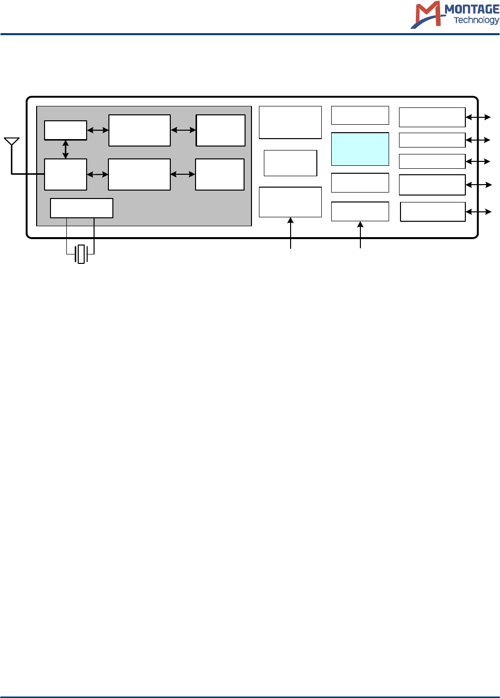
Functional Block Diagram
Figure 1. Functional Block Diagram for M88WI6800-K
ADC
40 MHz
2.4G Rx
Clock Gen
SRAM
T/R
Switch
PA 2.4G Tx DAC
802.11n 1x1
Baseband
802.11n
MAC
DCDC/LDO
32-bit
Processor
NVRAM
PMU
12-bit ADC
LED
802.11n
2.4 GHz RF
PWM / GPIO
SPI Flash
UART
802.11b/g/n Single-Chip Wi-Fi Micro Controller
M88WI6800-K
Montage Technology Proprietary and Confidential 3
1 Pin Information
1.1 Pin Assignment
Figure 2. QFN48 Pin Assignment
VDDA33
RF_TR_N
VDDA33
RF_TR_P
VDDA33
WLAN_LED
PD_N
PM_RES
VDDA33
XO
VDDA33
XI
VDDA33
VDDA33
GPIO2
GPIO1 / UART0_RXD
VDD33
GNDA
GPIO0 / UART0_TXD
GPIO3
GPIO5
GPIO4
GNDD
VDD12
GNDD
GPIO7 / PWM1 / UART1_RXD
GPIO8 / PWM2
GPIO6 / PWM0 / UART1_TXD
GPIO9 / PWM3
ADC_IN1
GNDA
VDDA33
BUCK_LX
VDDA33
GPIO12 / SPI_DI
GPIO11 / SPI_DO
GPIO18
GPIO13 / SPI_CK
GPIO14
VDDA33
VDDA33
M88WI6800-K
ADC_IN0
1
2
3
4
5
6
7
8
9
10
11
12
48 47 46 45 44 43 42 41 40 39 38 37
36
35
34
33
32
31
30
29
28
27
26
25
13 14 15 16 17 18 19 20 21 22 23 24
VDDA33
GPIO17
GPIO16
GPIO10 / SPI_CS
VDD33
VDD12
802.11b/g/n Single-Chip Wi-Fi Micro Controller
M88WI6800-K
Montage Technology Proprietary and Confidential 4
1.2 Pin List
Table 1. Signals By Pin Number
Pin No. Signal Name Pin No. Signal Name Pin No. Signal Name Pin No. Signal Name
1 RF_TR_P 13 VDDA33 25 GNDA 37 VDD33
2 RF_TR_N 14 VDDA33 26 BUCK_LX 38 GPIO10 / SPI_CS
3 VDDA33 15 GNDA 27 VDDA33 39 GPIO11 / SPI_DO
4WLAN_LED 16
GPIO0 /
UART0_TXD 28 ADC_IN1 40 GPIO12 / SPI_DI
5PD_N 17
GPIO1 /
UART0_RXD 29 ADC_IN0 41 GPIO13 / SPI_CK
6 VDDA33 18 GPIO2 30 VDDA33 42 GPIO14
7PM_RES 19GPIO3 31
GPIO6 / PWM0 /
UART1_TXD 43 GPIO16
8 VDDA33 20 VDD33 32 GPIO7 / PWM1 /
UART1_RXD 44 GPIO17
9 VDDA33 21 GNDD 33 GPIO8 / PWM2 45 GPIO18
10 VDDA33 22 VDD12 34 GPIO9 / PWM3 46 VDDA33
11 XI 23 GPIO4 35 VDD12 47 VDDA33
12 XO 24 GPIO5 36 GNDD 48 VDDA33

802.11b/g/n Single-Chip Wi-Fi Micro Controller
M88WI6800-K
Montage Technology Proprietary and Confidential 5
1.3 Pin Description
Table 2. Pin Description (Sheet 1 of 2)
Pin Name Pin No. Type1Description
RF Transceiver Interface
RF_TR_P 1 RF Differentia RF input/output (plus), or
Single-ended RF input/output.
RF_TR_N 2 RF Differentia RF input/output (minus), or
GNDA for Single-ended mode.
DCDC Converter Interface
BUCK_LX 26 AO Analog output of DCDC converter.
ADC Input Interface
ADC_IN1 28 AI Analog input 1 of ADC.
ADC_IN0 29 AI Analog input 0 of ADC.
GPIOs
GPIO[3:0] 19,18,17,16 I/O General purpose input/output pins.
GPIO[5:4] 24,23 I/O General purpose input/output pins.
GPIO[9:6] 34,33,32,31 I/O General purpose input/output pins.
GPIO10 38 I/O General purpose input/output pin.
This is also a Boot-strap pin which should be pulled High.
GPIO11 39 I/O General purpose input/output pin.
This is also a Boot-strap pin which should be pulled Low.
GPIO12 40 I/O General purpose input/output pin.
GPIO13 41 I/O General purpose input/output pin.
This is also a Boot-strap pin which should be pulled Low.
GPIO[18:16] &
GPIO14 45,44,43,42 I/O General purpose input/output pins.
Multiplexed UART Interfaces
UART0_RXD 17 I UART receive pin.
This pin is multiplexed with GPIO1.
UART0_TXD 16 O UART transmit pin.
This pin is multiplexed with GPIO0.
UART1_RXD 32 I
UART receive pin.
This pin is multiplexed with GPIO7. It shall be connected to an external
pulled-up resistor of 10 kΩ.
UART1_TXD 31 O UART transmit pin.
This pin is multiplexed with GPIO6.
Multiplexed PWM Drivers
PWM[3:0] 34,33,32,31 O PWM driver outputs.
These pins are multiplexed with GPIO[9:6].
802.11b/g/n Single-Chip Wi-Fi Micro Controller
M88WI6800-K
Montage Technology Proprietary and Confidential 6
Multiplexed SPI Flash Interface
SPI_CS 38 O SPI flash device selection signal output.
This pin is multiplexed with GPIO10.
SPI_DO 39 O SPI flash data output line.
This pin is multiplexed with GPIO11.
SPI_DI 40 I SPI flash data input line.
This pin is multiplexed with GPIO12.
SPI_CK 41 O SPI flash clock output.
This pin is multiplexed with GPIO13.
LED Driver
WLAN_LED 4 I/O
WLAN activity LED driver. The WLAN LED blinks when there is traffic
on the port.
This is also a Boot-strap pin which should be pulled Low.
XTAL, System Control & Miscellaneous
XI 11 AI 40 MHz quartz crystal input, or
40 MHz reference clock input with XO pin left floating.
XO 12 AO 40 MHz quartz crystal output.
PD_N 5 I External power down pin. Low active.
The pin shall be connected to an external pulled-up resistor of 10 kΩ.
PM_RES 7 AIO Reference resistor.
A 1.2 kΩ resistor in 1% is required to be tied to ground.
Power & Ground
VDD33 20,37 Power 3.3 V power supply for digital I/O pads.
VDD12 22,35 Power 1.2 V power supply for digital core.
VDDA33 3,6,8,9,10,13,14,
27,30,46,47,48 Power 3.3 V power supply for analog part.
GNDD 21,36 Ground Digital ground.
GNDA 15,25 Ground Analog ground.
1. In the Type column: “I” stands for Digital Input; “O” for Digital Output; “I/O” for Digital Input/Output; “AI” for Analog Input;
“AO” for Analog Output; “AIO” for Analog Input/Output.
Table 2. Pin Description (Sheet 2 of 2)
Pin Name Pin No. Type1Description
802.11b/g/n Single-Chip Wi-Fi Micro Controller
M88WI6800-K
Montage Technology Proprietary and Confidential 7
2 Electrical Characteristics
2.1 Absolute Maximum Ratings
2.2 Recommended Operating Conditions
Table 3. Absolute Maximum Ratings1
1. Stresses above the absolute maximum ratings may cause permanent damage to the device. Exposure to conditions beyond the
absolute maximum ratings may affect the life and reliability of the device.
Symbol Parameter Rating Unit
Min. Max.
VDDA33 3.3V Power Supply for Analog -0.3 3.6 V
VDD33 3.3V Power Supply for Digital I/Os -0.3 3.6 V
VDD12 1.2V Power Supply for Digital Core -0.3 1.5 V
VIN Voltage on Input Pins -0.5 VDD33+0.5 V
TSTG Storage Temperature -40 +125 °C
VESD ESD Protection (HBM) - TBD V
Table 4. Recommended Operating Conditions1
1. Device functionality is not guaranteed at any conditions beyond the recommended operating conditions.
Symbol Parameters Min. Typ. Max. Unit
VDDA33 Analog Part Supply Voltage 2.97 3.3 3.6 V
VDD33 Digital Part DC Supply Voltage for Digital I/O 2.97 3.3 3.6 V
VDD12 Digital Part DC Supply Voltage for Digital Core 1.14 1.2 1.26 V
TAOperating Ambient Temperature -10 - 70 °C
802.11b/g/n Single-Chip Wi-Fi Micro Controller
M88WI6800-K
Montage Technology Proprietary and Confidential 8
2.3 DC Electrical Characteristics
2.4 Current Consumption
Table 5. DC Electrical Characteristics
Symbol Parameters Min. Typ. Max. Unit
VIL Low Level Input Voltage (for LVTTL) -0.28 0.6 V
VIH High Level Input Voltage (for LVTTL) 2.0 3.6 V
VT- Schmitt Trigger Negative Going Threshold
Voltage (for LVTTL) 0.68 1.36 V
VT+ Schmitt Trigger Positive Going Threshold
Voltage (for LVTTL) 1.36 1.7 V
VOL Low Level Output Voltage
(|OL| = 1.6~14mA) -0.28 0.4 V
VOH High Level Output Voltage
(|OH| = 1.6~14mA) 2.4 VDD33+0.33 V
Table 6. Current Consumption
Symbol Condition Min. Typ. Max. Unit
Itotal
Sleep mode TBD mA
Rx Active, HT40, MCS7 TBD mA
RX Power saving, DTIM=1 TBD mA
RX Listen TBD mA
TX HT40, MCS7 @13dBm TBD mA
TX CCK, 11Mbps @19dBm TBD mA
802.11b/g/n Single-Chip Wi-Fi Micro Controller
M88WI6800-K
Montage Technology Proprietary and Confidential 9
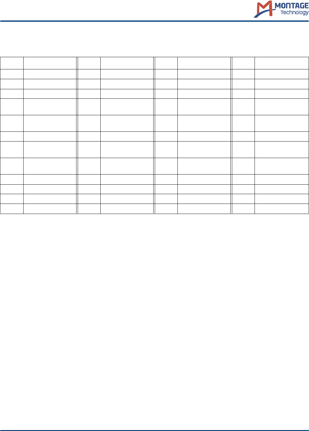
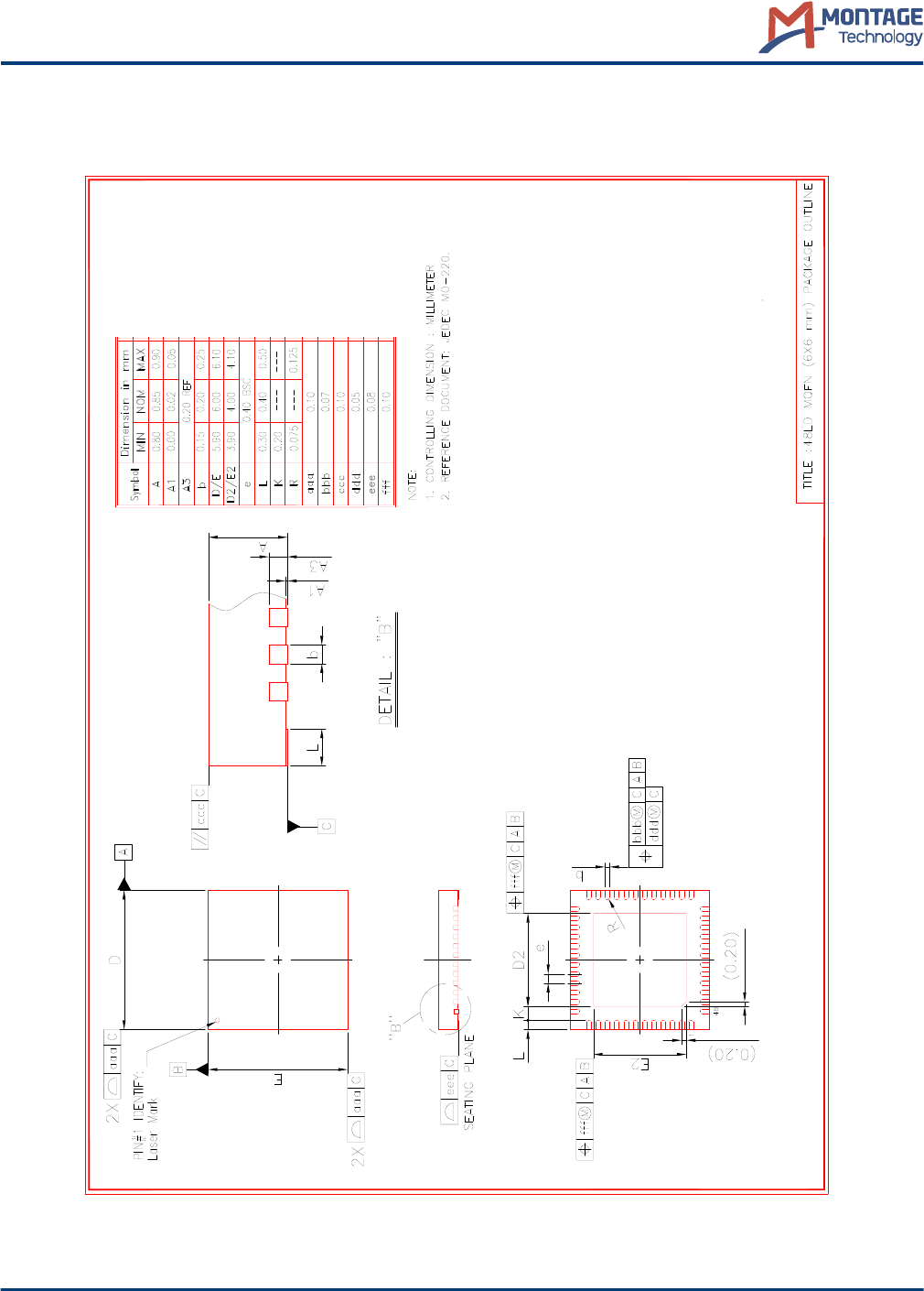
3 Mechanical Package Data
Figure 3. QFN48 Package Outline

Montage Technology Proprietary and Confidential 10
802.11b/g/n Single-Chip Wi-Fi Micro Controller
M88WI6800-K
Contact Information
Montage Technology (Shanghai) Co., Ltd.
Address: 6/F, Block A, Technology Building, 900 Yishan Road, Shanghai 200233, China
Phone: +86-21-6128-5678
Fax: +86-21-5426-3132
E-mail: infosh@montage-tech.com
Website: www.montage-tech.com
Montage Technology, Inc.
Address: 101 Metro Drive, Suite 500, San Jose, CA 95110, USA
Phone: +1-408-982-2788
Fax: +1-408-982-2789
E-mail: infosv@montage-tech.com
Website: www.montage-tech.com
Montage Sales Contact in Korea
Address: Suite 604, 6th Fl., B-dong, Woolim Lions Valley 5 Cha, Galmachi-ro 302, Jungwon-gu, Seongnam-si,
Gyeonggi-do, 462-739 Korea
Phone: +82-70-8247-4520
E-mail: infosk@montage-tech.com
Website: www.montage-tech.com
FCC
Federal Communications Commission (FCC) Statement
15.21
You are cautioned that changes or modifications not expressly approved by the part
responsible for compliance could void the user’s authority to operate the equipment.
15.105(b)
This equipment has been tested and found to comply with the limits for a Class B
digital device, pursuant to part 15 of the FCC rules. These limits are designed to
provide reasonable protection against harmful interference in a residential installation.
This equipment generates, uses and can radiate radio frequency energy and, if not
installed and used in accordance with the instructions, may cause harmful
interference to radio communications. However, there is no guarantee that
interference will not occur in a particular installation. If this equipment does cause
harmful interference to radio or television reception, which can be determined by
turning the equipment off and on, the user is encouraged to try to correct the
interference by one or more of the following measures:
-Reorient or relocate the receiving antenna.
-Increase the separation between the equipment and receiver.
-Connect the equipment into an outlet on a circuit different from that to which the
receiver is connected.
-Consult the dealer or an experienced radio/TV technician for help.
This device complies with Part 15 of the FCC Rules. Operation is subject to the
following two conditions:
1) this device may not cause harmful interference and
2) this device must accept any interference received, including interference that may
cause undesired operation of the device.
FCC RF Radiation Exposure Statement:
1. This Transmitter must not be co-located or operating in conjunction with any other
antenna or transmitter.
2. This equipment complies with RF radiation exposure limits set forth for an uncontrolled
environment.
FCC RF Radiation Exposure Statement:
1. This Transmitter must not be co-located or operating in conjunction with any other
antenna or transmitter.
2. For body worn operation, this device has been tested and meets FCC RF exposure
guidelines. When used with an accessory that contains metal may not ensure compliance
with FCC RF exposure guidelines.
End Product Labeling
This transmitter module is authorized only for use in devices where the antenna
may be installed such that 20 centimeter may be maintained between the antenna
and users. The final end product must be labeled in visible area with the following:
“Contains FCC ID: 2AEDFWM6800K”
Manual Information to the End user
The OEM integrator has to be aware not to provide information to the end user
regarding how to install or remove this RF module in the user’s manual of the end
product which integrates this module.
The end user manual shall include all required regulatory information/warning as
show in this manual.
NCC
低功率電波輻射性電機管理辦法
第十二條: 經型式認證合格之低功率射頻電機,非經許可,公司、商號或使用者均不
得擅自變更頻率、加大功率或變更原設計之特性及功能。
第十四條: 低功率射頻電機之使用不得影響飛航安全及干擾合法通信;經發現有干擾
現象時,應立即停用,並改善至無干擾時方得繼續使用。低功率射頻電機需忍受合法
通信或工業、科學及醫療用電波輻射性電機設備之干擾。
此模組於取得認證後將依規定於模組本體標示審驗合格標籤,並要求平台廠商於平台
上標示「本產品內含射頻模組:ID 編號」字樣。