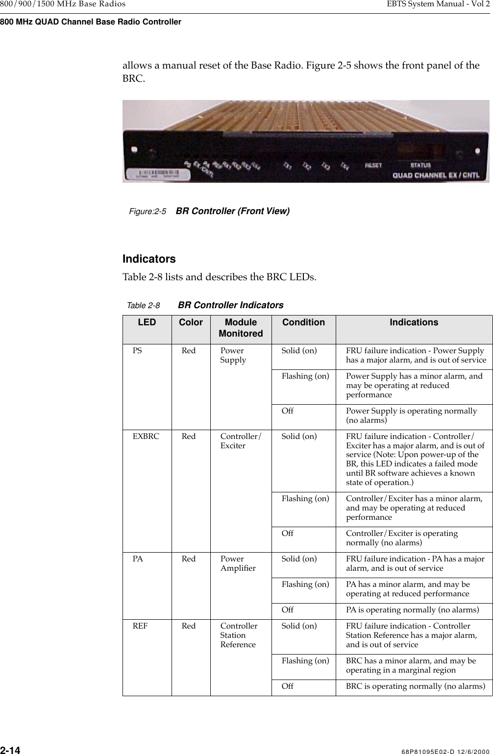
Motorola Solutions 89FC5794 Enhanced Base Transceiver System (EBTS) User Manual Quad BR 800 Tx FCC Filing
Motorola Solutions, Inc. Enhanced Base Transceiver System (EBTS) Quad BR 800 Tx FCC Filing
UserManual.wiki
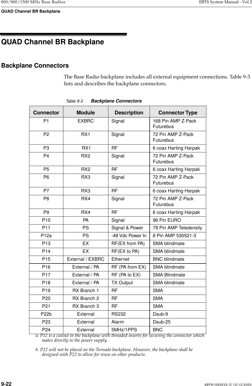
>
Motorola Solutions
>
89FC5794 User Manual
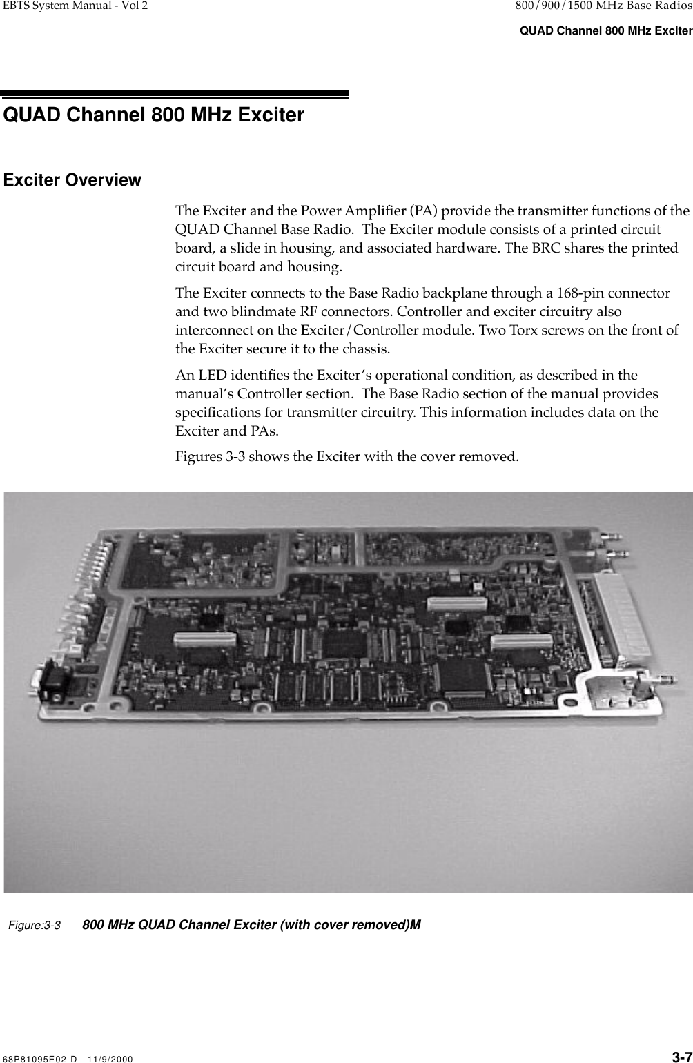
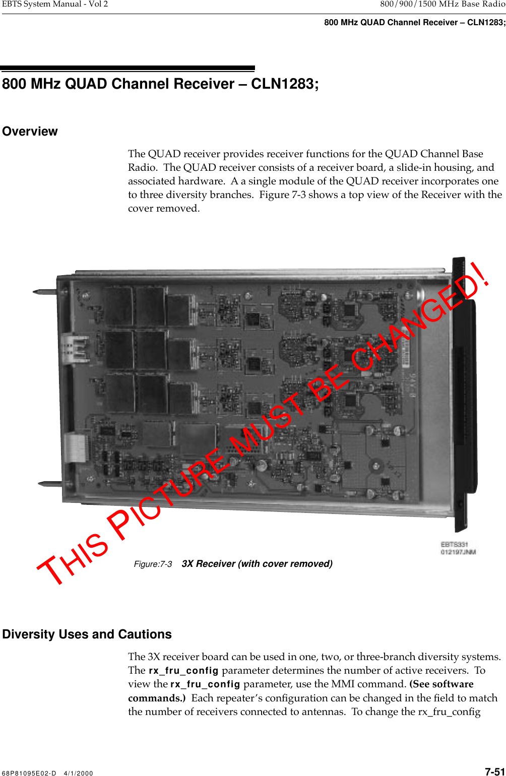
Exhibit D Users Manual
Navigation menu
Upload a User Manual
Namespaces
Wiki Guide
HTML
PDF
Info
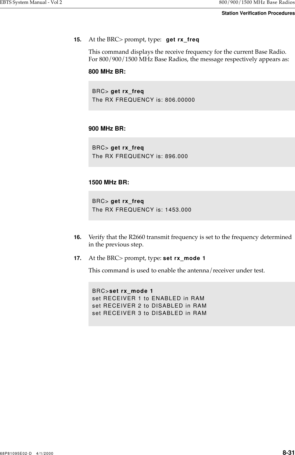
Views
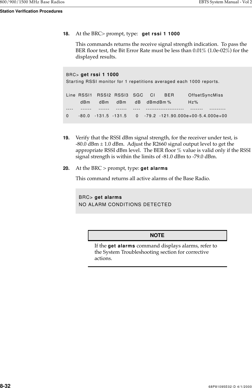
User Manual
Discussion / Help
Navigation


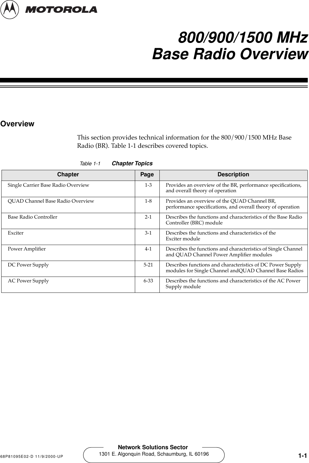


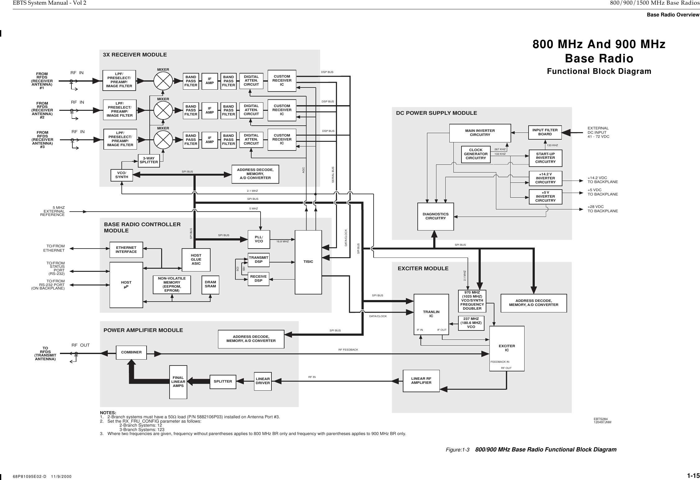
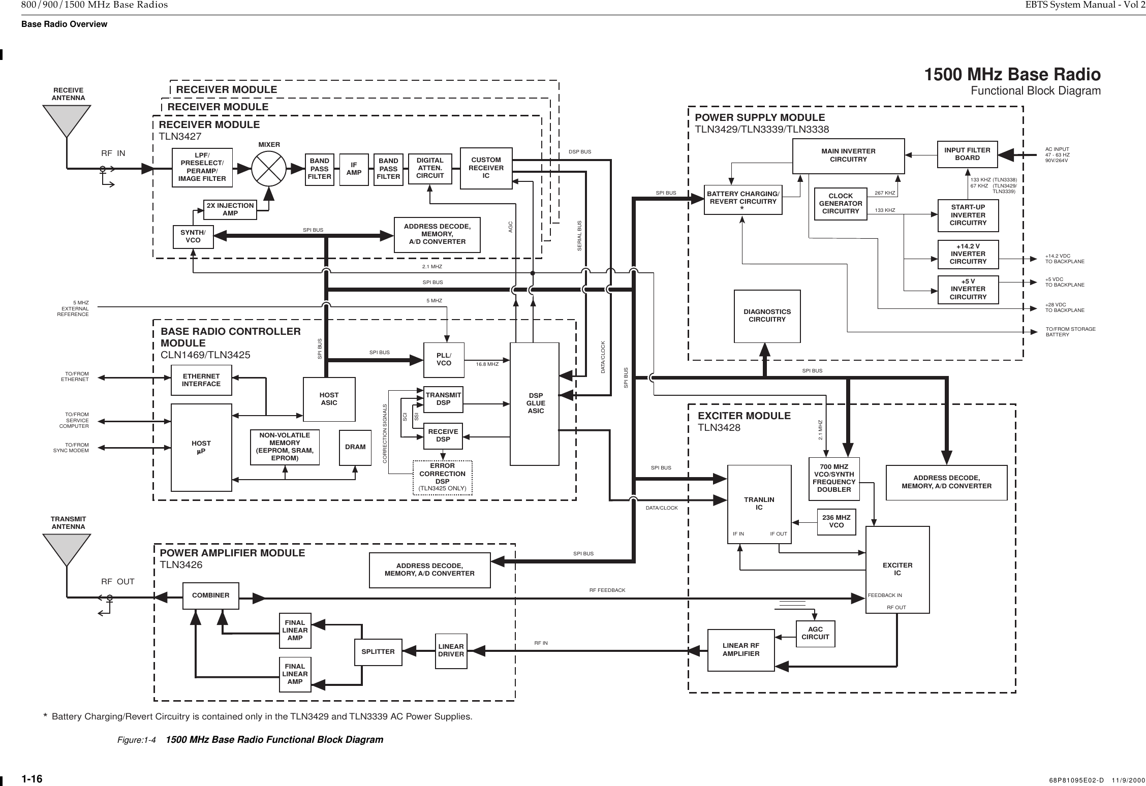
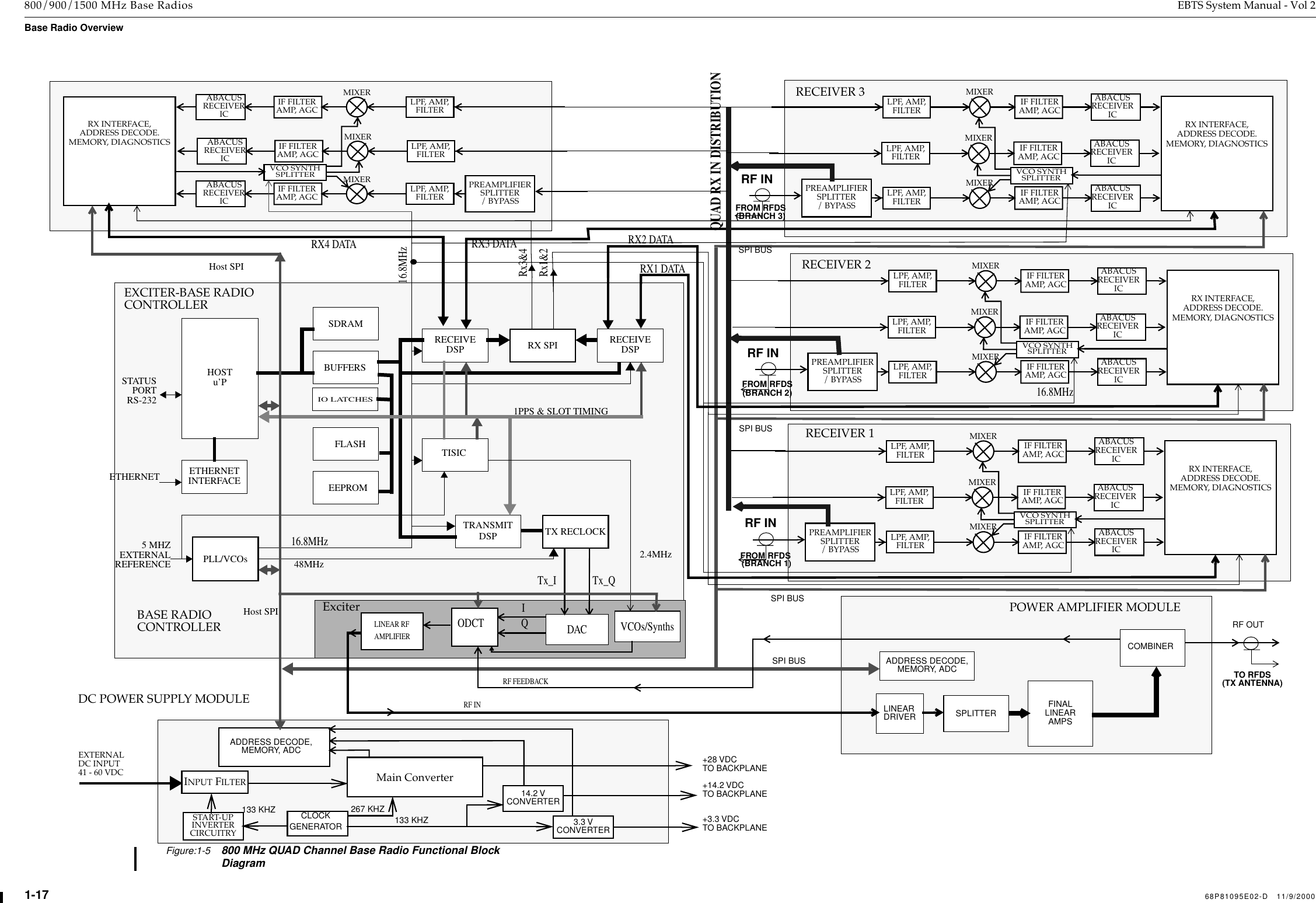

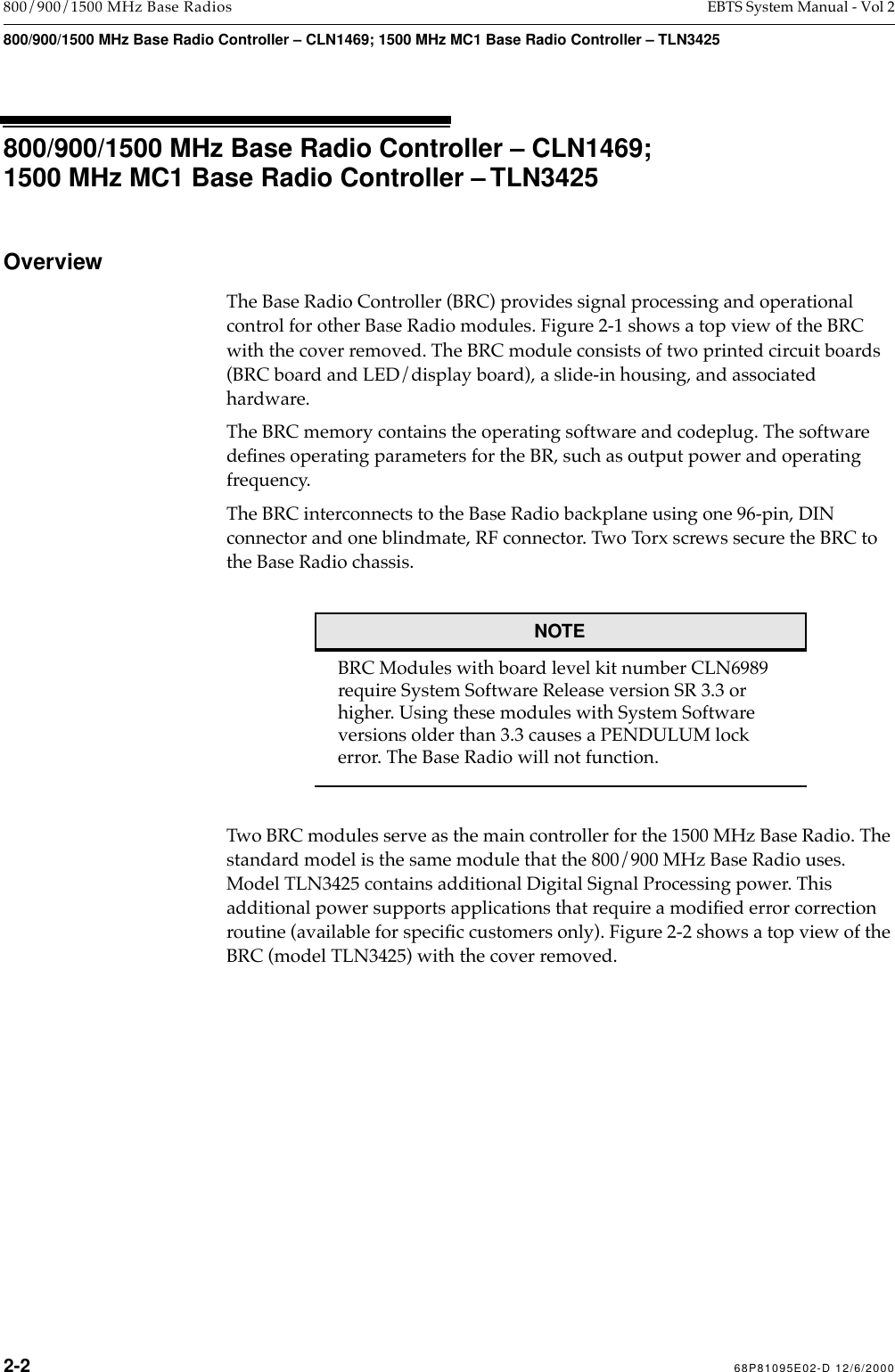
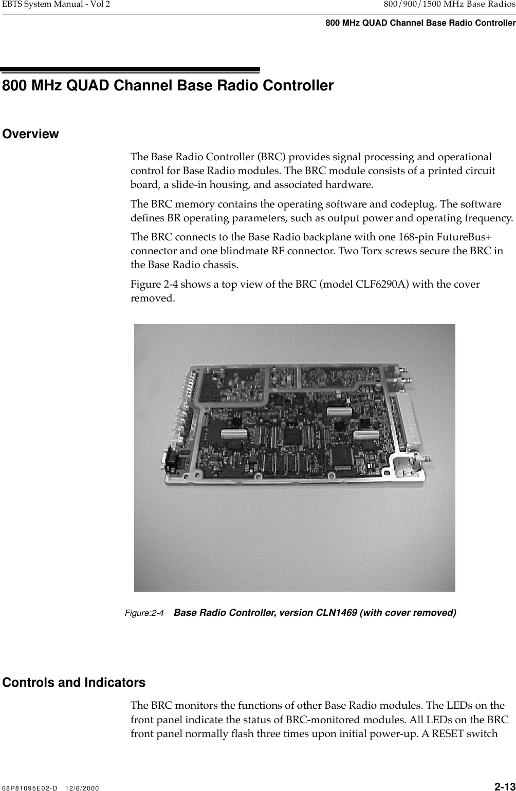


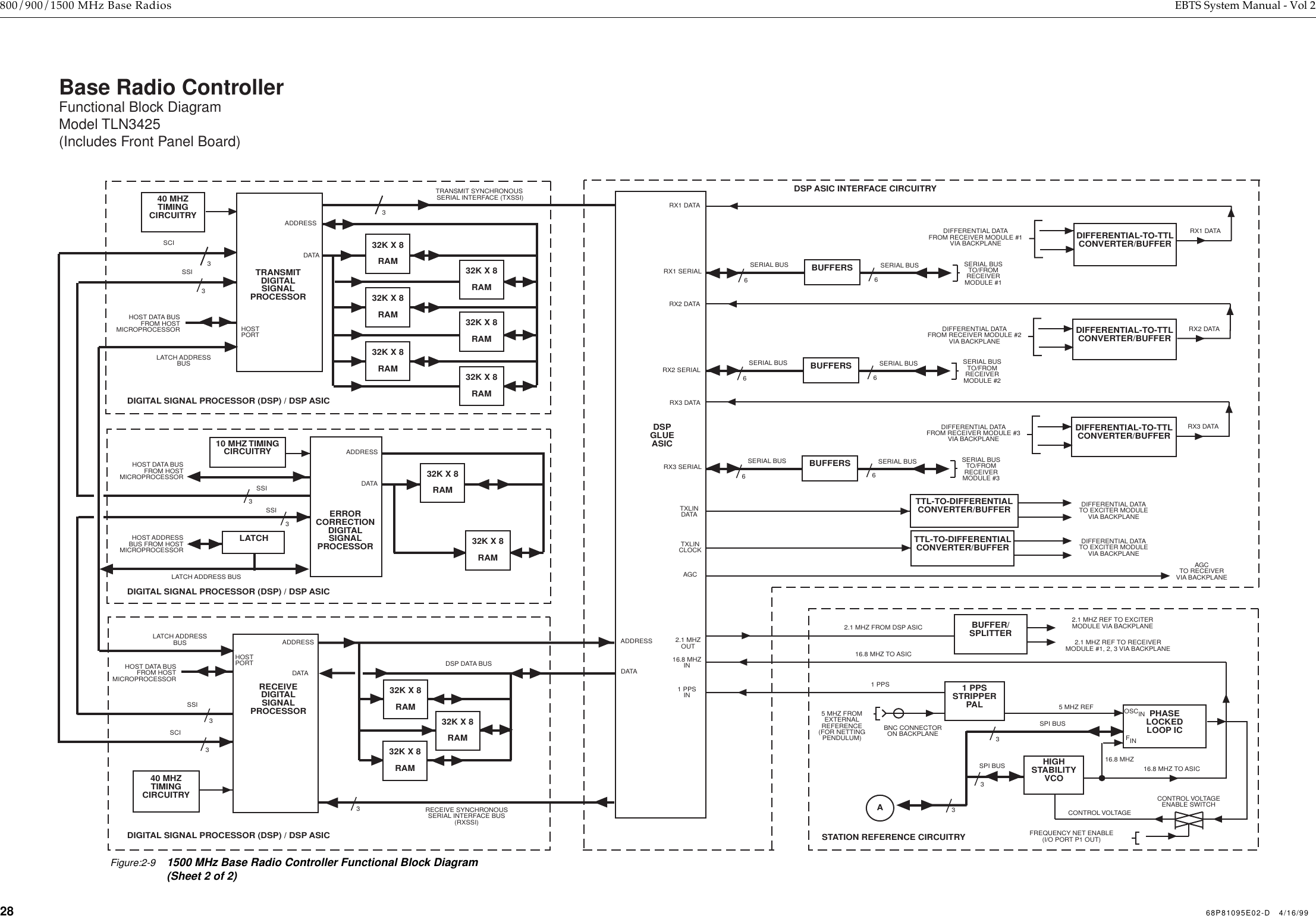
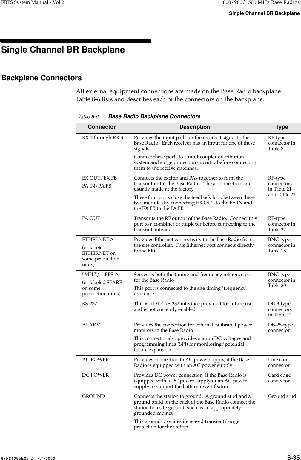
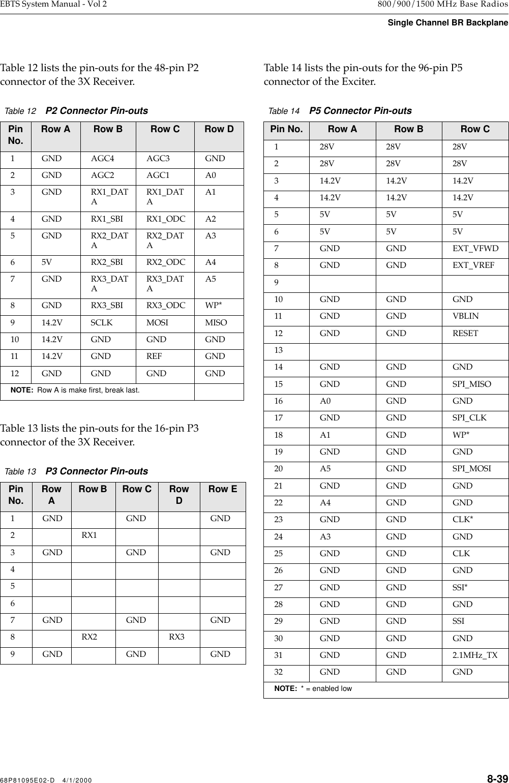
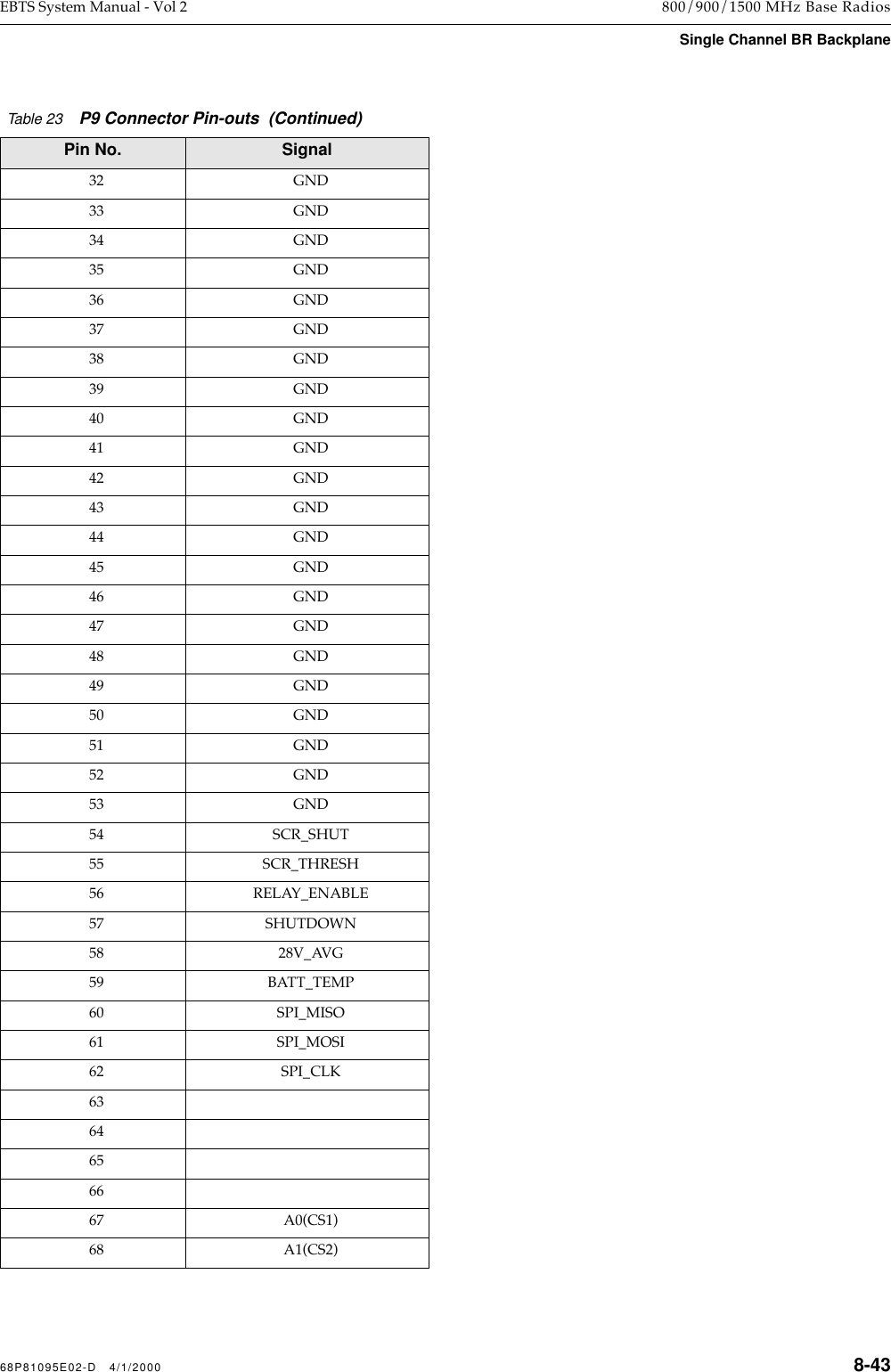
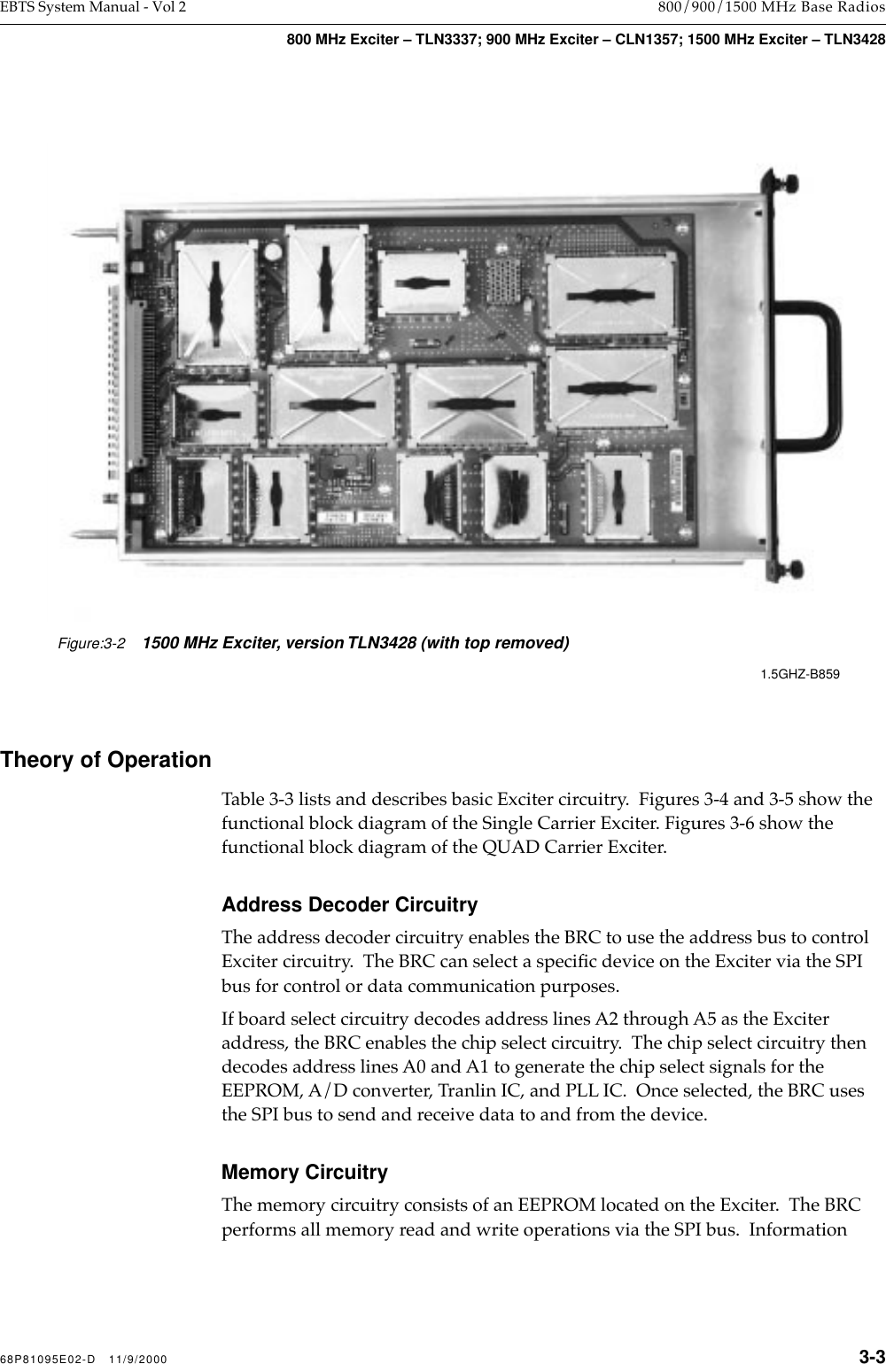
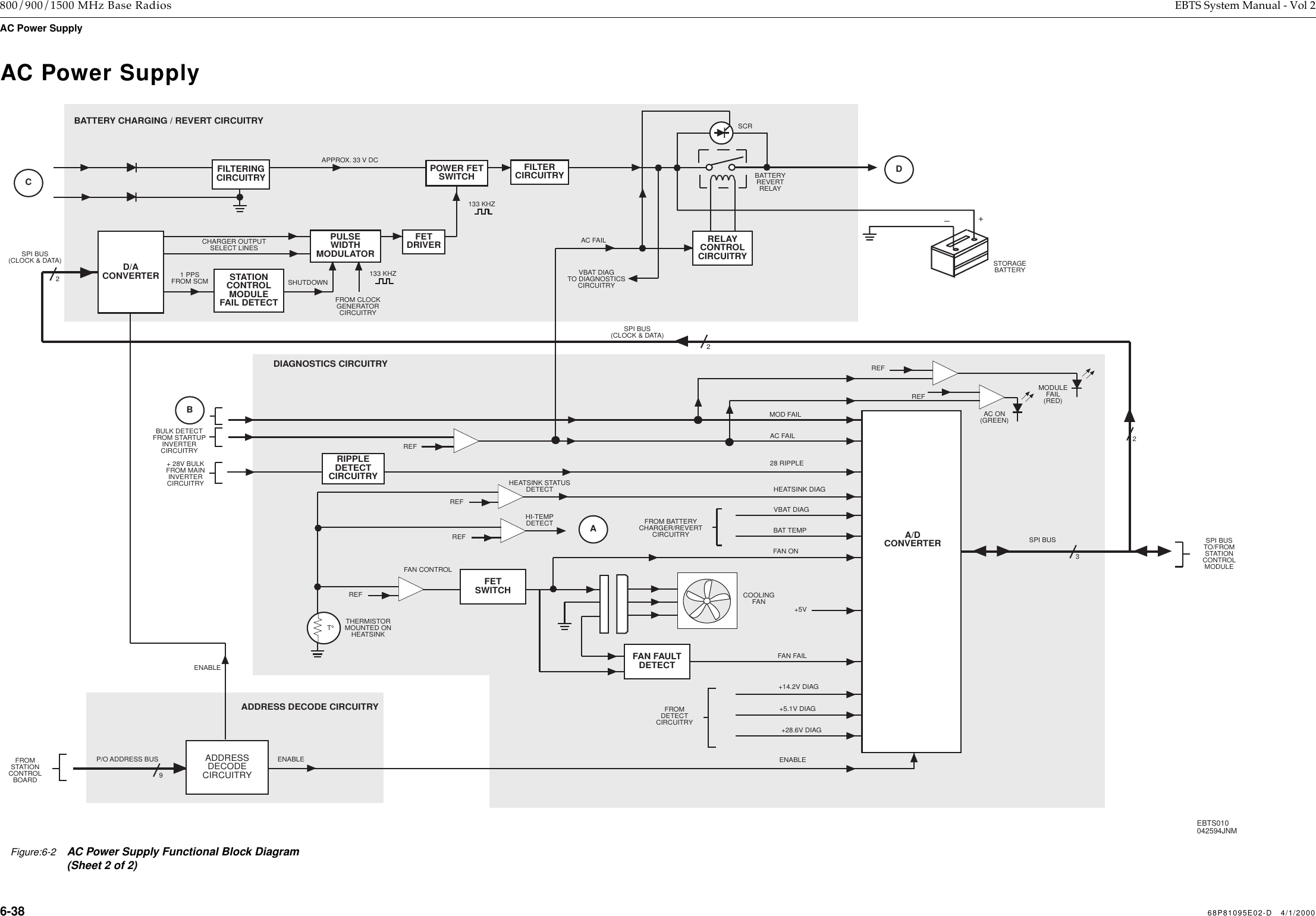
![2--30 68P81095E02-D 12/4/2000 800/900/1500 MHz Base Radios EBTS System Manual - Vol 2 Base Radio Controller QUAD Channel Base Radio ControllerFunctional Block DiagramFigure:2-11QUAD CHANNEL Base Radio Controller Functional Block Diagram(Sheet 2 of 2)HOSTMICRO-ETHERNETSERIALINTERFACETRANS-CDRCV RXTRMT TXCLSN10BASE2COAXETHERNETSERIALINTERFACECEIVERISOLATIONTRANSFORMERPROCESSORSCC18SDRAM4M x 16SDRAM4M x 16SDRAM4M x 16SDRAM4M x 16GPLA0, A[8,9,17,18,20:29],RAS,CAS,WECS2CS3D[0:31]D[0:15]D[16:31]D[0:15]D[16:31]BUFFERBUFFERBUFFERBUFFERBUFFERBUFFERD[0:31]D[0:7]A[10:31]MA[21:0]DSP_D[31:24]A[0:7]DSP_A[31:24]MD[31:0]EIA-232BUSRECEIVERS/DRIVERS2STATUS PORT(9 PIN D CONNECTORON BRC FRONT PANEL)2BUFFER33SPI BUS TO/FROM STATION MODULESFLASH1M x 16FLASH1M x 16FLASH1M x 16FLASH1M x 16CS0CS1MD[0:15]MD[16:31]MD[0:15]MD[16:31]1616161616 161616MA[2:21]MA[2:21]EEPROM32k x 8MD[24:31]MA[0:14]CS4P1_OUTLATCHP0_OUTLATCHMD[0:32]MD[24:31]P0_INBUFFERMD[16,17,20-24,28-31]STATUS BUSFROMSTATION MODULESP0_IN8CONTROL BUSTOSTATION MODULESP0_OUT/P1_OUT328TRANSMITDIGITALSIGNALPROCESSOR(TX DSP)SINGLE ENDTO DIFFERENTIALTRANSMITCLOCK ANDFRAME SYNCHCIRCUITRYI/Q DATASERIAL DATATO EXCITERDIFFERENTIALTO SINGLE ENDRX1 SERIAL DATARECEIVEDIGITALSIGNALPROCESSOR(RX DSP 1)RECEIVEDIGITALSIGNALPROCESSOR(RX DSP 2)TISICA[0:5]D[0, 8:23]PARALLELTO SERIALCIRCUITRYD[16:23]D[16:23]D[0, 23]SPI BUS TORECEIVER 1 & 2SPI BUS TORECEIVER 3 & 42.4 MHz1 PPS TIMING, CONTROL/ SLOT TIMING/RESETNETWORKEDSCI16.8MHZ48 MHZSPIBUSSPIBUSEXCITERSPICONTROLDSP SPISPI BUSTO EXCITERDIGITAL SIGNAL PROCESSING CIRCUITRYDIGITAL SIGNAL PROCESSING CIRCUITRYDIFFERENTIALTO SINGLE ENDDIFFERENTIALTO SINGLE ENDDIFFERENTIALTO SINGLE END50 MHZCLOCKFRONT PANELRESETDRAM MEMORYETHERNET INTERFACENON-VOLATILE MEMORY EXPANDED STATUS INPUTAND OUTPUT CONTROL CIRCUITRYEXTENDED HOSTBUS BUFFERS40TO EXCITER5MHZ1PPSRX2 SERIAL DATARX3 SERIAL DATARX4 SERIAL DATAHOST ADDRESS BUSHOST DATA BUSHOST BUFFERED DATA BUSHOST BUFFERED ADDRESS BUSHOST-DSP BUFFERED DATA BUSHOST-DSP BUFFERED ADDRESS BUSSERIAL MANAGEMENT CONTROLLER (SMC2)SERIAL PERIPHERAL INTERFACE](https://usermanual.wiki/Motorola-Solutions/89FC5794/User-Guide-133969-Page-64.png)


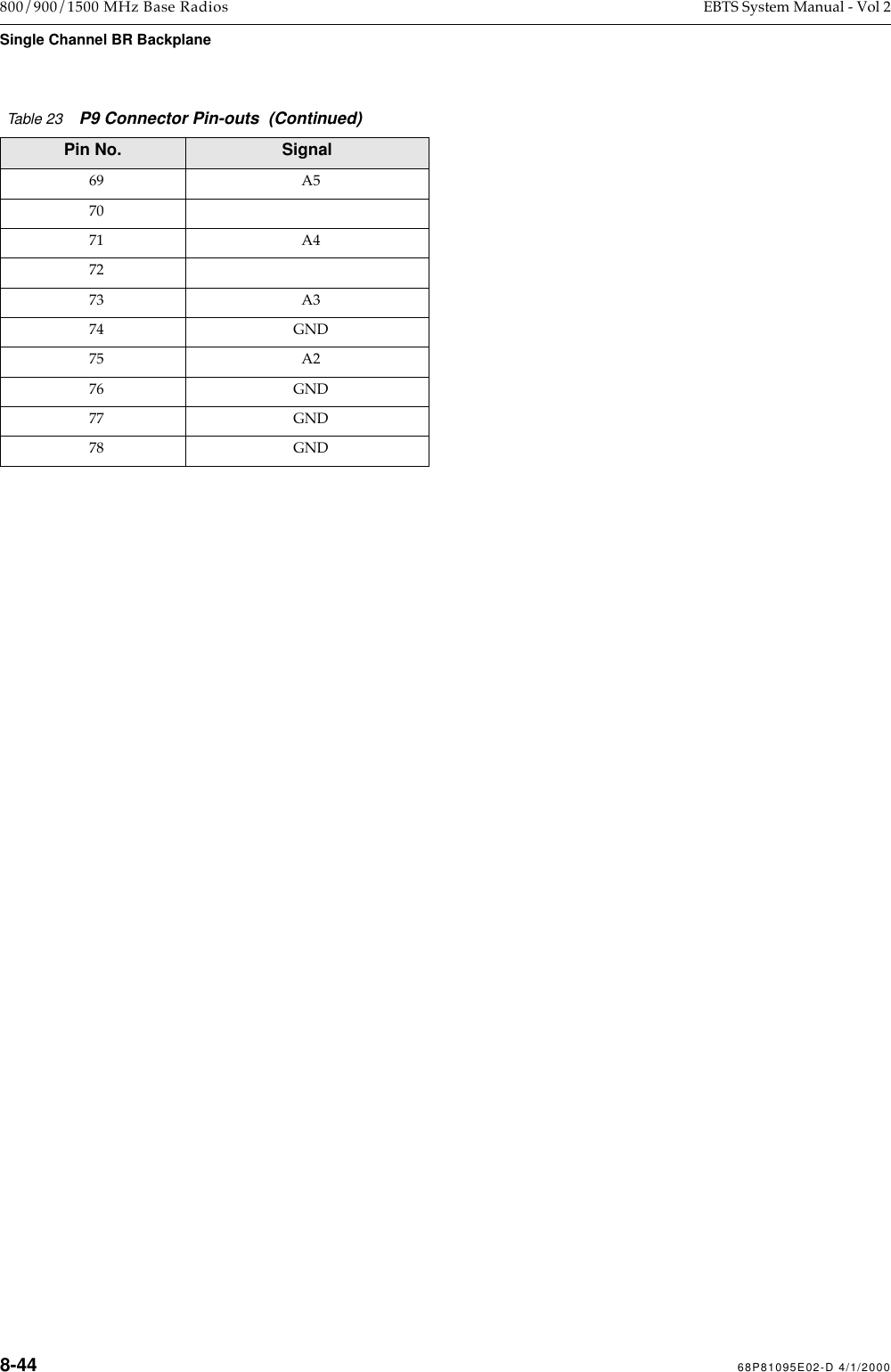
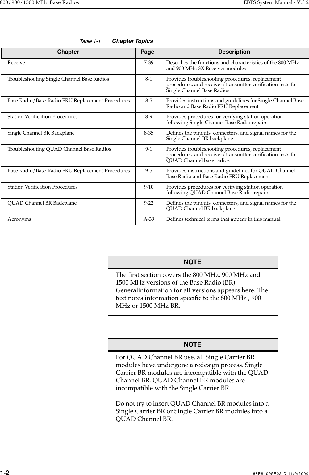
![68P81095E02-D 4/1/2000 8-13EBTS System Manual - Vol 2 800/900/1500 MHz Base RadiosStation Verification Procedures4. At the BRC> prompt, type: set tx_power 40This command sets the transmitter output to 40 Watts. After keying the Base Radio, verify the forward and reßected powers of the station along with the station VSWR with the parameters listed in Table 8-2. 5. At the BRC> prompt, type: get fwd_pwrThis command returns the current value of forward power from the RF Power AmpliÞer.Table 8-240W, 800 MHz PA Transmitter ParametersParameter Value or RangeForward Power Greater than 38.0 WattsReßected Power Less than 4.0 WattsVSWR Less than 2:1BRC> set tx_power 40setting transmitter power to 40 wattsTXLIN ATTENUATION: 5.000000TARGET POWER: 40.00 watts [46.02 dBm]ACTUAL POWER: 37.77 watts [45.07 dBm]POWER WINDOW: 38.20-> 41.89 watts [45.82 -> 46.22 dBm]TXLIN LEVEL REGISTER REDUCED 59 STEPS [-2.30 dB].TXLIN LEVEL: 0x6fcompleted successfullyBRC> get fwd_pwrFORWARD POWER is 39.13 watts [45.92 dBm]](https://usermanual.wiki/Motorola-Solutions/89FC5794/User-Guide-133969-Page-151.png)
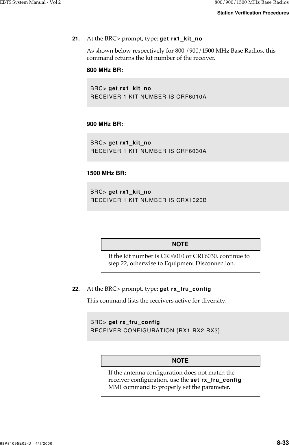
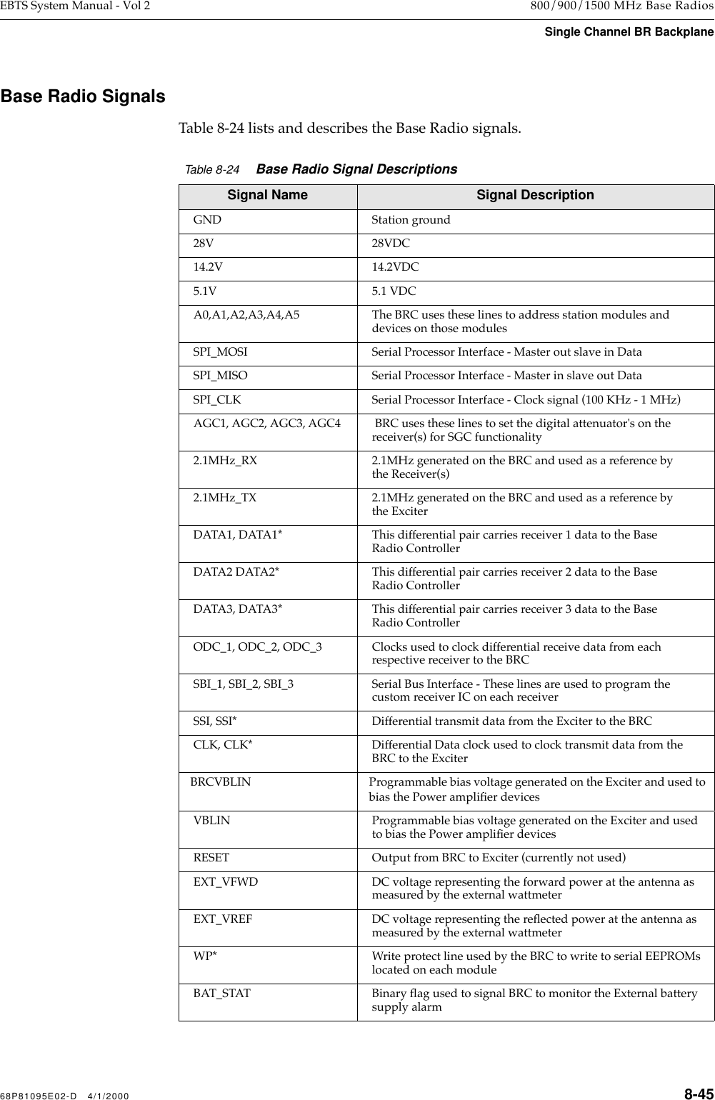
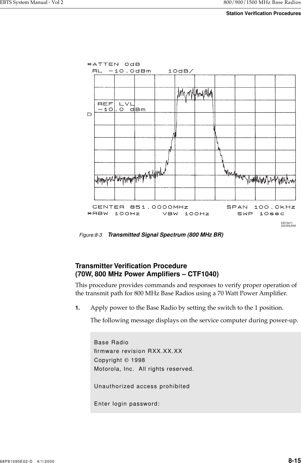
![8-14 68P81095E02-D 4/1/2000800/900/1500 MHz Base Radios EBTS System Manual - Vol 2Station Verification Procedures6. At the BRC> prompt, type: get ref_pwrThis command returns the current value of reßected power from the RF Power AmpliÞer.7. At the BRC> prompt, type: get vswrThis command calculates the current Voltage Standing Wave Ratio (VSWR) from the RF Power AmpliÞer.8. At the BRC> prompt, type: get alarmsThis command returns all active alarms of the Base Radio.NOTEIf the get alarms command displays alarms, refer to the System Troubleshooting section of this manual for corrective actions.9. View the spectrum of the transmitted signal on the R2660 Communications Analyzer in the Spectrum Analyzer mode. Figure 8-3 shows a sample of the spectrum.10. At the BRC> prompt, type: dekey This command stops all transmitter activity.BRC> get ref_pwrREFLECTED POWER is 0.27 watts [24.28 dBm]BRC> get vswrVSWR is 1.17:1BRC> get alarmsNO ALARM CONDITIONS DETECTEDBRC> dekeyXMIT OFF INITIATED](https://usermanual.wiki/Motorola-Solutions/89FC5794/User-Guide-133969-Page-152.png)

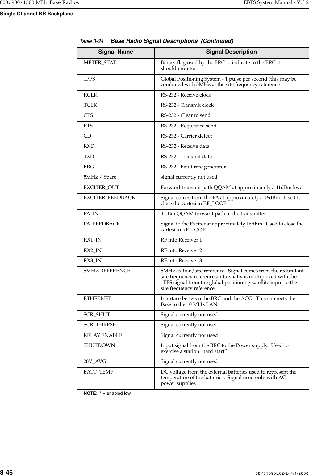
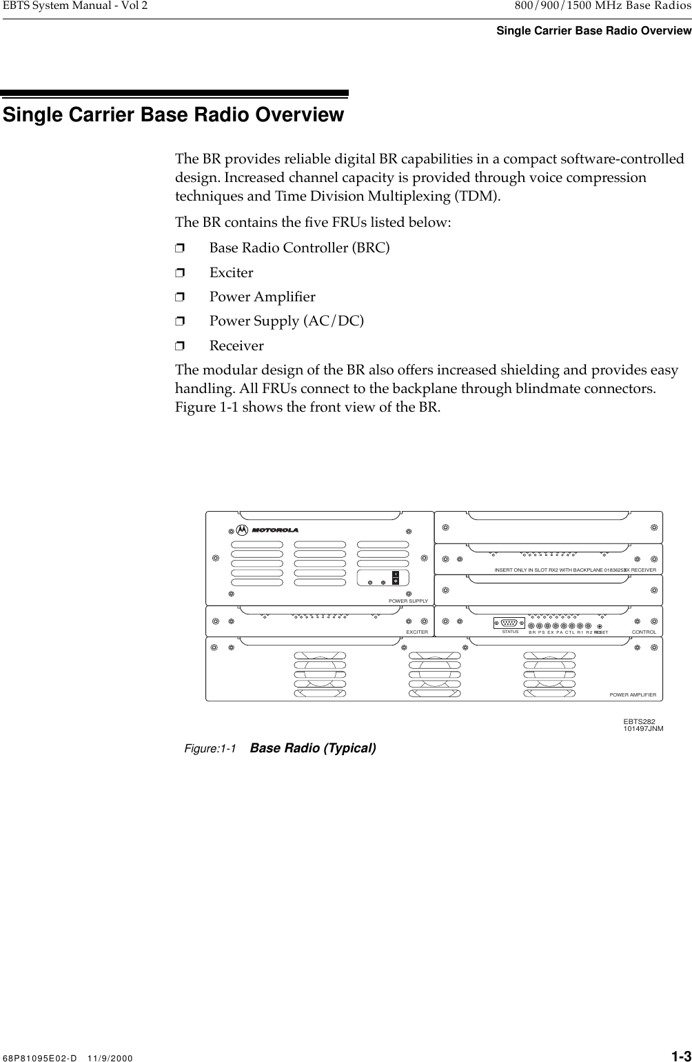
![68P81095E02-D 4/1/2000 8-17EBTS System Manual - Vol 2 800/900/1500 MHz Base RadiosStation Verification Procedures4. At the BRC> prompt, type: set tx_power 70This command sets the transmitter output to 70 Watts. After keying the Base Radio, verify the forward and reßected powers of the station along with the station VSWR with the parameters listed in Table 8-3.5. At the BRC> prompt, type: get fwd_pwrThis command returns the current value of forward power from the RF Power AmpliÞer.Table 8-370W, 800 MHz PA Transmitter ParametersParameter Value or RangeForward Power Greater than 66.5 WattsReßected Power Less than 7.0 WattsVSWR Less than 2:1BRC> set tx_power 70setting transmitter power to 70 wattsTXLIN ATTENUATION: 5.000000TARGET POWER: 70.00 watts [48.45 dBm]ACTUAL POWER: 56.70 watts [47.54 dBm]POWER WINDOW: 66.85 -> 73.30 watts [48.25 -> 48.65 dBm]TXLIN LEVEL REGISTER REDUCED 85 STEPS [-3.32 dB].TXLIN LEVEL: 0x55completed successfullyBRC> get fwd_pwrFORWARD POWER is 68.55 watts [48.36 dBm]](https://usermanual.wiki/Motorola-Solutions/89FC5794/User-Guide-133969-Page-155.png)
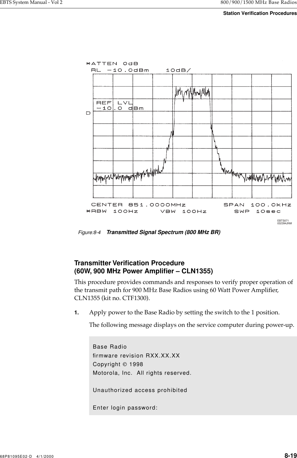
![8-18 68P81095E02-D 4/1/2000800/900/1500 MHz Base Radios EBTS System Manual - Vol 2Station Verification Procedures6. At the BRC> prompt, type: get ref_pwrThis command returns the current value of reßected power from the RF Power AmpliÞer.7. At the BRC> prompt, type: get vswrThis command calculates the current Voltage Standing Wave Ratio (VSWR) from the RF Power AmpliÞer.8. At the BRC> prompt, type: get alarmsThis command returns all active alarms of the Base Radio.NOTEIf the get alarms command displays alarms, refer to the System Troubleshooting section of this manual for corrective actions.9. View the spectrum of the transmitted signal on the R2660 Communications Analyzer in the Spectrum Analyzer mode. Figure 8-4 shows a sample of the spectrum.10. At the BRC> prompt, type: dekey This command stops all transmitter activity.BRC> get ref_pwrREFLECTED POWER is 2.10 watts [33.22 dBm]BRC> get vswrVSWR is 1.42:1BRC> get alarmsNO ALARM CONDITIONS DETECTEDBRC> dekeyXMIT OFF INITIATED](https://usermanual.wiki/Motorola-Solutions/89FC5794/User-Guide-133969-Page-156.png)

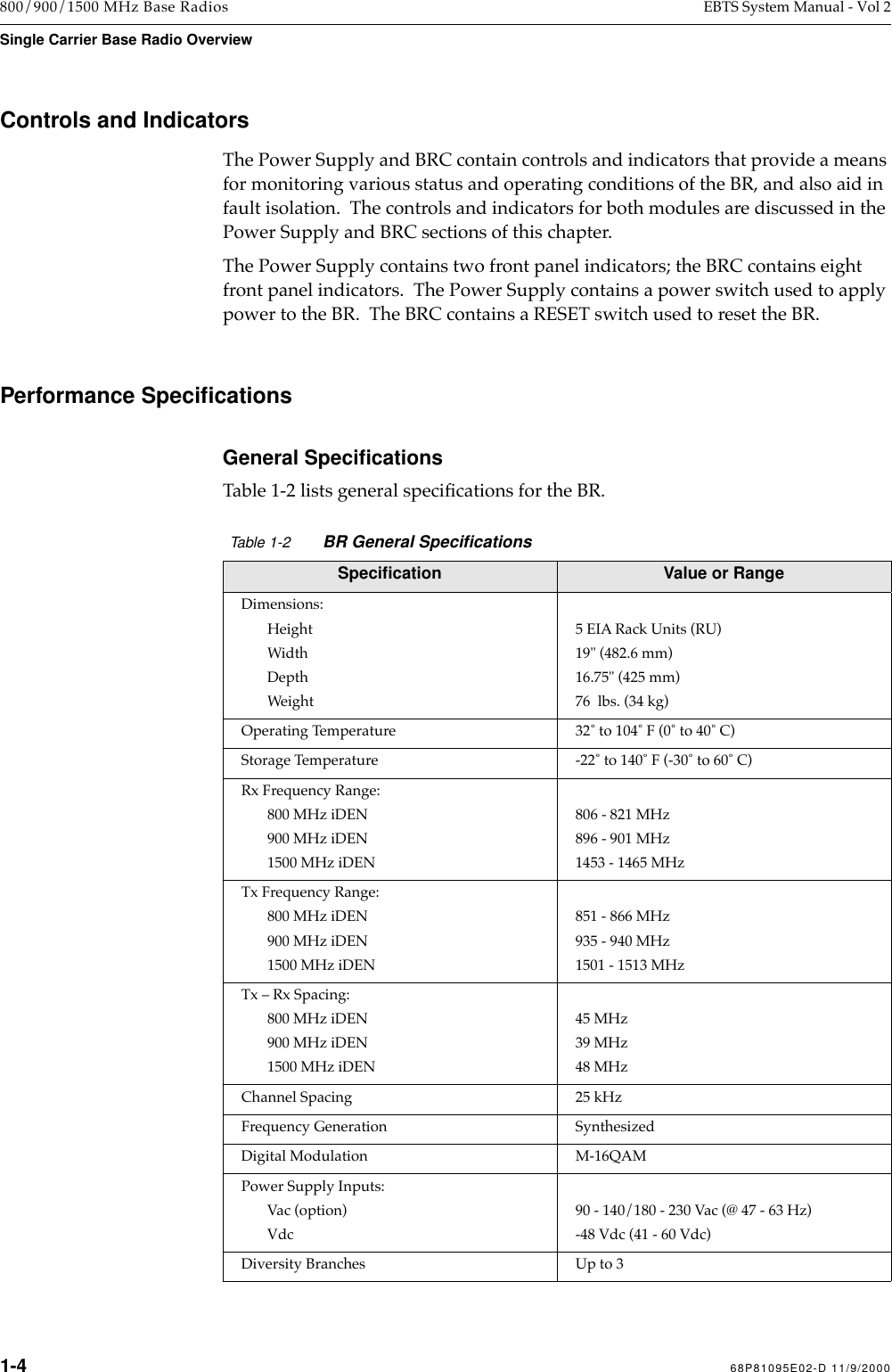
![68P81095E02-D 4/1/2000 8-21EBTS System Manual - Vol 2 800/900/1500 MHz Base RadiosStation Verification Procedures4. At the BRC> prompt, type: set tx_power 60This command sets the transmitter output to 60 Watts. After keying the Base Radio, verify the forward and reßected powers of the station along with the station VSWR with the parameters listed in Table 8-4.5. At the BRC> prompt, type: get fwd_pwrThis command returns the current value of forward power from the RF Power AmpliÞer.Table 8-460W, 900 MHz PA – CLN1355 Transmitter ParametersParameter Value or RangeForward Power Greater than 58.0 WattsReßected Power Less than 6.0 WattsVSWR Less than 2:1BRC> set tx_power 60setting transmitter power to 60 wattsTXLIN ATTENUATION: 5.000000TARGET POWER: 60.00 watts [47.78 dBm]ACTUAL POWER: 56.70 watts [47.54 dBm]POWER WINDOW: 57.30 -> 62.85 watts [47.58 -> 47.98 dBm]TXLIN LEVEL REGISTER REDUCED 85 STEPS [-3.32 dB].TXLIN LEVEL: 0x55completed successfullyBRC> get fwd_pwrFORWARD POWER is 61.0 watts [47.88 dBm]](https://usermanual.wiki/Motorola-Solutions/89FC5794/User-Guide-133969-Page-159.png)
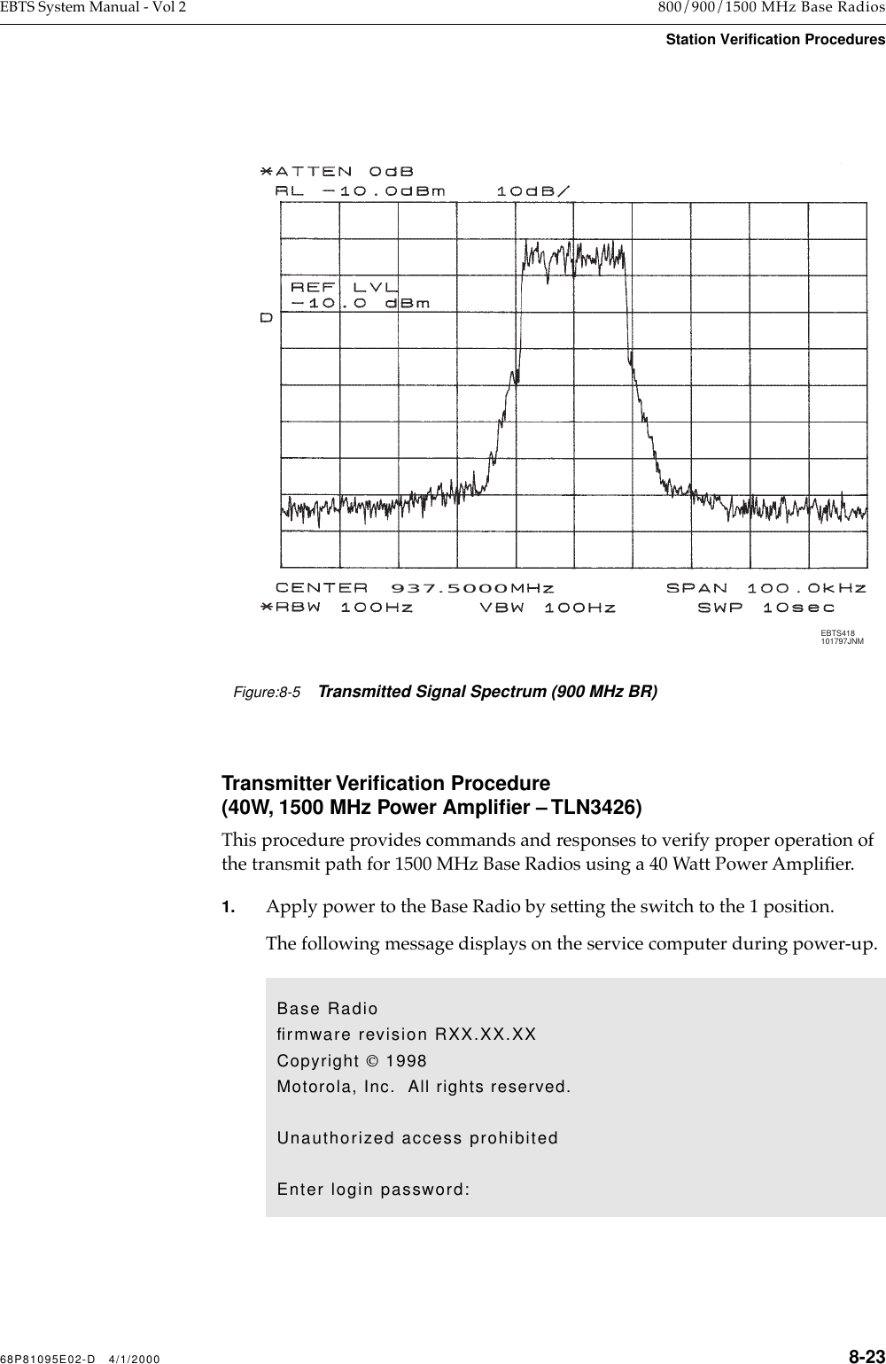
![8-22 68P81095E02-D 4/1/2000800/900/1500 MHz Base Radios EBTS System Manual - Vol 2Station Verification Procedures6. At the BRC> prompt, type: get ref_pwrThis command returns the current value of reßected power from the RF Power AmpliÞer.7. At the BRC> prompt, type: get vswrThis command calculates the current Voltage Standing Wave Ratio (VSWR) from the RF Power AmpliÞer.8. At the BRC> prompt, type: get alarmsThis command returns all active alarms of the Base Radio.NOTEIf the get alarms command displays alarms, refer to the System Troubleshooting section of this manual for corrective actions.9. View the spectrum of the transmitted signal on the R2660 Communications Analyzer in the Spectrum Analyzer mode. Figure 8-5 shows a sample of the spectrum.10. At the BRC> prompt, type: dekey This command stops all transmitter activity.BRC> get ref_pwrREFLECTED POWER is 1.67 watts [32.22 dBm]BRC> get vswrVSWR is 1.42:1BRC> get alarmsNO ALARM CONDITIONS DETECTEDBRC> dekeyXMIT OFF INITIATED](https://usermanual.wiki/Motorola-Solutions/89FC5794/User-Guide-133969-Page-160.png)
![68P81095E02-D 4/1/2000 8-25EBTS System Manual - Vol 2 800/900/1500 MHz Base RadiosStation Verification Procedures4. At the BRC> prompt, type: set tx_power 40This command sets the transmitter output to 40 Watts. After keying the Base Radio, verify the forward and reßected powers of the station along with the station VSWR with the parameters listed in Table 8-5. 5. At the BRC> prompt, type: get fwd_pwrThis command returns the current value of forward power from the RF Power AmpliÞer.Table 8-540W, 1500 MHz PA Transmitter ParametersParameter Value or RangeForward Power Greater than 38.0 WattsReßected Power Less than 4.0 WattsVSWR Less than 2:1BRC> set tx_power 40setting transmitter power to 40 wattsTXLIN ATTENUATION: 5.000000TARGET POWER: 40.00 watts [46.02 dBm]ACTUAL POWER: 28.38 watts [44.53 dBm]POWER WINDOW: 38.20-> 41.89 watts [45.82 -> 46.22 dBm]TXLIN LEVEL REGISTER REDUCED 59 STEPS [-2.30 dB].TXLIN LEVEL: 0x6fcompleted successfullyBRC> get fwd_pwrFORWARD POWER is 39.13 watts [45.92 dBm]](https://usermanual.wiki/Motorola-Solutions/89FC5794/User-Guide-133969-Page-163.png)
![8-26 68P81095E02-D 4/1/2000800/900/1500 MHz Base Radios EBTS System Manual - Vol 2Station Verification Procedures6. At the BRC> prompt, type: get ref_pwrThis command returns the current value of reßected power from the RF Power AmpliÞer.7. At the BRC> prompt, type: get vswrThis command calculates the current Voltage Standing Wave Ratio (VSWR) from the RF Power AmpliÞer.8. At the BRC> prompt, type: get alarmsThis command returns all active alarms of the Base Radio.NOTEIf the get alarms command displays alarms, refer to the System Troubleshooting section of this manual for corrective actions.9. View the spectrum of the transmitted signal on the R2660 Communications Analyzer in the Spectrum Analyzer mode. Figure 8-3 shows a sample of the spectrum.10. At the BRC> prompt, type: dekey This command stops all transmitter activity.BRC> get ref_pwrREFLECTED POWER is 0.27 watts [24.28 dBm]BRC> get vswrVSWR is 1.17:1BRC> get alarmsNO ALARM CONDITIONS DETECTEDBRC> dekeyXMIT OFF INITIATED](https://usermanual.wiki/Motorola-Solutions/89FC5794/User-Guide-133969-Page-164.png)