Motorola Solutions 89FC5794 Enhanced Base Transceiver System (EBTS) User Manual Quad BR 800 Tx FCC Filing
Motorola Solutions, Inc. Enhanced Base Transceiver System (EBTS) Quad BR 800 Tx FCC Filing
Exhibit D Users Manual

APPLICANT: MOTOROLA INC. EQUIPMENT TYPE: ABZ89FC5794
EXHIBIT 8
INSTRUCTION MANUALS
The instruction and service manual for this base radio are not published at this time. However, draft copy of the
manual is available and has been included as part of the filing package in the form of an electronic pdf document.
Upon request, published and/or printed manuals will be sent to the commission and/or telecommunication
certification body (TCB) as soon as they become available. All of the descriptions and schematics included this
filing package are up to date.

APPLICANT: MOTOROLA INC. EQUIPMENT TYPE: ABZ89FC5794
EXHIBIT 9
TUNE-UP PROCEDURE
There is no field tune-up procedure. All adjustments are software controlled and are pre-set at the factory. Certain
station operating parameters can be changed via man-machine interface (MMI) commands, within predetermined
limits. Examples include transmit / receiver operating frequencies and power level.

68P81099E10-D
ECCN 5E992
Network Solutions Sector
ENHANCED BASE TRANSCEIVER SYSTEM (EBTS)
VOLUME 2 OF 3
BASE RADIOS
© 2000 Motorola, Inc.
All Rights Reserved
Printed in U.S.A.
FCC INTERFERENCE WARNING
The FCC requires that manuals pertaining to Class A computing devices must contain warnings about possible interference with local residential radio and TV reception. This
warning reads as follows:
Note: This equipment has been tested and found to comply with the limits for a Class A digital device, pursuant to Part 15 of the FCC Rules. These limits
are designed to provide reasonable protection against harmful interference when the equipment generates, uses, and can radiate radio frequency
energy and, if not installed and used in accordance with the instruction manual, may cause harmful interference to radio communications. Operation of
this equipment in a residential area is likely to cause harmful interference in which case the user will be required to correct the interference at his own
expense.
INDUSTRY OF CANADA NOTICE OF COMPLIANCE
This Class A digital apparatus meets all requirements of the Canadian Interference-Causing Equipment Regulations.
Cet appareil numérique de la classe A respecte toutes les exigences du Règlement sur le matériel brouilleur du Canada.
COMMERCIAL WARRANTY (STANDARD)
Motorola radio communications products (the “Product”) is warranted to be free from defects in material and workmanship for a period of ONE (1) YEAR (except for crystals and
channel elements which are warranted for a period of ten (10 years) from the date of shipment. Parts including crystals and channel elements, will be replaced free of charge for
the full warranty period but the labor to replace defective parts will only be provided for One Hundred-Twenty (120) days from the date of shipment. Thereafter purchaser must
pay for the labor involved in repairing the Product or replacing the parts at the prevailing rates together with any transportation charges to or from the place where warranty
service is provided. This express warranty is extended by Motorola, 1301 E. Algonquin Road, Schaumburg, Illinois 60196 to the original end use purchaser only, and only to
those purchasing for purpose of leasing or solely for commercial, industrial, or governmental use.
THIS WARRANTY IS GIVEN IN LIEU OF ALL OTHER WARRANTIES EXPRESS OR IMPLIED WHICH ARE SPECIFICALLY EXCLUDED, INCLUDING WARRANTIES OF
MERCHANTABILITY OR FITNESS FOR A PARTICULAR PURPOSE. IN NO EVENT SHALL MOTOROLA BE LIABLE FOR INCIDENTAL OR CONSEQUENTIAL DAMAGES TO
THE FULL EXTENT SUCH MAY BE DISCLAIMED BY LAW.
In the event of a defect, malfunction or failure to conform to specifications established by Motorola, or if appropriate to specifications accepted by Motorola in writing, during the
period shown, Motorola, at its option, will either repair or replace the product or refund the purchase price thereof. Repair at Motorola's option, may include the replacement of
parts or boards with functionally equivalent reconditioned or new parts or boards. Replaced parts or boards are warranted for the balance of the original applicable warranty
period. All replaced parts or product shall become the property of Motorola.
This express commercial warranty is extended by Motorola to the original end user purchaser or lessee only and is not assignable or transferable to any other party. This is the
complete warranty for the Product manufactured by Motorola. Motorola assume no obligations or liability for additions or modifications to this warranty unless made in writing and
signed by an officer of Motorola. Unless made in a separate agreement between Motorola and the original end user purchaser, Motorola does not warrant the installation,
maintenance or service of the Products.
Motorola cannot be responsible in any way for any ancillary equipment not furnished by Motorola which is attached to or used in connection with the Product, or for operation of
the Product with any ancillary equipment, and all such equipment is expressly excluded from this warranty. Because each system which may use Product is unique, Motorola
disclaims liability for range, coverage, or operation of the system as a whole under this warranty.
This warranty does not cover:
a) Defects or damage resulting from use of the Product in other than its normal and customary manner.
b) Defects or damage from misuse, accident, water or neglect
c) Defects or damage from improper testing, operation, maintenance installation, alteration, modification, or adjusting.
d) Breakage or damage to antennas unless caused directly by defects in material workmanship.
e) A Product subjected to unauthorized Product modifications, disassemblies or repairs (including without limitation, the addition to the Product of non-Motorola supplied
equipment) which adversely affect performance of the Product or interfere with Motorola's normal warranty inspection and testing of the Product to verify any warranty claim.
f) Product which has had the serial number removed or made illegible.
g) A Product which, due to illegal to unauthorized alteration of the software/firmware in the Product, does not function in accordance with Motorola's published specifications or
the FCC type acceptance labeling in effect for the Product at the time the Product was initially distributed from Motorola.
This warranty sets forth the full extent of Motorola's responsibilities regarding the Product. Repair, replacement or refund of the purchase date, at Motorola’s option is the
exclusive remedy. IN NO EVENT SHALL MOTOROLA BE LIABLE FOR DAMAGES IN EXCESS OF THE PURCHASE PRICE OF THE PRODUCT, FOR ANY LOSS OF USE,
LOSS OR TIME, INCONVENIENCE, COMMERCIAL LOSS, LOST PROFITS OR SAVINGS OR OTHER INCIDENTAL, SPECIAL OR CONSEQUENTIAL DAMAGE ARISING
OUT OF THE USE OR INABILITY TO USE SUCH PRODUCT, TO THE FULL EXTENT SUCH MAY BE DISCLAIMED BY LAW.
SOFTWARE NOTICE/WARRANTY
Laws in the United States and other countries preserve for Motorola certain exclusive rights for copyrighted Motorola software such as the exclusive rights to reproduce in copies
and distribute copies of such Motorola software. Motorola software may be used in only the Product in which the software was originally embodied and such software in such
Product may not be replaced, copied, distributed, modified in any way, or used to produce any derivative thereof. No other use including without limitation alteration, modification,
reproduction, distribution, or reverse engineering of such Motorola software or exercise of rights in such Motorola software is permitted. No license is granted by implication,
estoppel or otherwise under Motorola patent rights or copyrights.
This warranty extends only to individual products: batteries are excluded, but carry their own separate limited warranty.
In order to obtain performance of this warranty, purchaser must contact its Motorola salesperson or Motorola at the address first above shown, attention Quality Assurance
Department.
This warranty applies only within the fifty (50) United States and the District of Columbia.

68P81099E10-D 4/1/2000-UP
i
Network Solutions Sector
1301 E. Algonquin Road, Schaumburg, IL 60196
1 Contents
Contents.......................................................................................................................... i
List of Figures .............................................................................................................. iv
List of Tables................................................................................................................ vi
Foreword................................................................................................................................. ix
General Safety Information .................................................................................................... xi
800/900/1500 MHz
Base Radio Overview...............................................................................................1-1
Single Carrier Base Radio Overview.................................................................................... 1-4
QUAD Channel Base Radio Overview ................................................................................ 1-9
800/900/1500 MHz Base Radio Controller – CLN1469;
1500 MHz MC1 Base Radio Controller – TLN3425 ................................................2-1
800 MHz QUAD Channel Base Radio Controller .............................................................2-12
800 MHz Exciter – TLN3337;
900 MHz Exciter – CLN1357;
1500 MHz Exciter – TLN3428...................................................................................5-1
QUAD Channel 800 MHz Exciter ....................................................................................... 5-7
QUAD-Channel Power Amplifiers: 40W, 800 MHz – TLF2020 (TTF1580);
70W, 800 MHz – TLN3335 (CTF1040);
60W, 900 MHz – CLN1355 (CLF1300);
40W, 1500 MHz – TLN3426;
800 MHz QUAD – CLF1400 ......................................................................................6-1
Theory of Operation .............................................................................................................6-6
DC Power Supply for QUAD Channel Base Radios...............................................7-1
QUAD CHANNEL DC Power Supply................................................................................. 7-4
AC Power Supply .......................................................................................................8-1
800 MHz 3X Receiver – CLN1283;
900 MHz 3X Receiver – CLN1356............................................................................9-1
1500 MHz Receiver – TLN3427.......................................................................................... 9-8

ii
68P81099E10-D-C 4/1/2000
Contents EBTS System Manual - Vol 2
800 MHz QUAD Channel Receiver – CLN1283;.............................................................. 9-12
Troubleshooting Single Channel Base Radios .................................................... 10-1
Base Radio/Base Radio FRU Replacement Procedures ..................................................... 10-5
Station Verification Procedures.......................................................................................... 10-9
Single Channel BR Backplane.......................................................................................... 10-35
Troubleshooting QUAD Channel Base Radios..................................................... 11-1
Base Radio/Base Radio FRU Replacement Procedures ..................................................... 11-5
Station Verification Procedures........................................................................................ 11-10
QUAD Channel BR Backplane ........................................................................................ 11-22
QUAD Base Radio Signals............................................................................................... 11-35
Transmitter & Receiver Verification Procedures for Beta- Release Equipment 12-1
Acronyms .....................................................................................................................13
Index ....................................................................................................................Index-1

iii
68P81099E10-D 4/1/2000
Contents EBTS System Manual - Vol 2
This Page Intentionally
Left Blank

iv
68P81099E10-D 1/15/2000
Contents EBTS System Manual - Vol 2
List of Figures
List of Figures
Figure:1-1
Base Radio (Typical) ..................................................................................................................... 1-4
Figure:1-2
QUAD Channel Base Radio (Typical) .......................................................................................... 1-9
Figure:1-3
800/900 MHz Base Radio Functional Block Diagram ................................................................ 1-15
Figure:1-4
1500 MHz Base Radio Functional Block Diagram ..................................................................... 1-16
Figure:1-5
800 MHz QUAD Channel Base Radio Functional Block Diagram ............................................ 1-17
Figure:2-1
Base Radio Controller, version CLN1469 (with cover removed) ................................................. 2-2
Figure:2-2
Base Radio Controller, version TLN3425 (with cover removed).................................................. 2-2
Figure:2-3
BR Controller (Front View)........................................................................................................... 2-3
Figure:2-4
Base Radio Controller, version CLN1469 (with cover removed) ............................................... 2-12
Figure:2-5
BR Controller (Front View)......................................................................................................... 2-13
Figure:2-6
800/900 MHz Base Radio Controller Functional Block Diagram
(Sheet 1 of 2) ................................................................................................................................2-23
Figure:2-6
800/900 MHz Base Radio Controller Functional Block Diagram
(Sheet 2 of 2) ................................................................................................................................2-24
Figure:2-7
1500 MHz Base Radio Controller Functional Block Diagram
(Sheet 1 of 2) ................................................................................................................................2-25
Figure:2-8
1500 MHz Base Radio Controller Functional Block Diagram (Sheet 2 of 2)............................. 2-26
Figure:2-7
QUAD CHANNEL Base Radio Controller Functional Block Diagram
(Sheet 1 of 2) ................................................................................................................................2-27
Figure:2-7
QUAD CHANNEL Base Radio Controller Functional Block Diagram
(Sheet 2 of 2) ................................................................................................................................2-28
Figure:3-1
800/900 MHz Exciter (with cover removed)................................................................................. 5-2
Figure:3-2
1500 MHz Exciter, version TLN3428 (with top removed) ........................................................... 5-3
Figure:3-3
800 MHz QUAD Channel Exciter (with cover removed) ............................................................. 5-7
Figure:3-4
Exciter Functional Block Diagram .............................................................................................. 3-11
Figure:3-5
Exciter Functional Block Diagram .............................................................................................. 3-12
Figure:3-6
Exciter Functional Block Diagram .............................................................................................. 3-13
Figure:3-7
Exciter Functional Block Diagram .............................................................................................. 3-14
Figure:4-1
70W, 800 MHz PA – TLN3335 (with cover removed)................................................................. 6-2
Figure:4-2
60W, 900 MHz PA – CLN1355 (with cover removed)................................................................. 6-3
Figure:4-3
40W, 1500 PA (with cover removed)............................................................................................ 6-4
Figure:4-4
QUAD Channel PA (with cover removed).................................................................................... 6-5
Figure:4-5
TLF2020 (TTF1580B) 40 W, 800 MHz Power Amplifier Functional Block Diagram
(Sheet 1 of 1)................................................................................................................................ 4-13
Figure:4-6
TLN3335 (CTF1040) 70 W, 800 MHz Power Amplifier Functional Block Diagram
(Sheet 1 of 1)................................................................................................................................ 4-14
Figure:4-7
60W, 900 MHz Power Amplifier Functional Block Diagram
(Sheet 1 of 1)................................................................................................................................ 4-15

68P81099E10-D 1/15/2000
v
EBTS System Manual - Vol 2 Contents
List of Figures
Figure:4-8
Power Amplifier Functional Block Diagram............................................................................... 4-16
Figure:4-9
QUAD Channel Power Amplifier Functional Block Diagram (Sheet 1 of 1)............................. 6-17
Figure:5-1
DC Power Supply .......................................................................................................................... 7-2
Figure:5-2
Quad Carrier Power Supply........................................................................................................... 7-4
Figure:5-3
DC Power Supply Functional Block Diagram
(Sheet 1 of 2) ..................................................................................................................................7-7
Figure:5-3
DC Power Supply Functional Block Diagram
(Sheet 2 of 2) ..................................................................................................................................7-8
Figure:5-3
QUAD Channel DC Power Supply Functional Block Diagram
(Sheet 1 of 2).................................................................................................................................. 7-9
Figure:5-3
QUAD Channel DC Power Supply Functional Block Diagram
(Sheet 2 of 2) ................................................................................................................................7-10
Figure:6-1
AC Power Supply (front view) ...................................................................................................... 8-2
Figure:6-2
AC Power Supply Functional Block Diagram (Sheet 1 of 2)........................................................ 8-5
Figure:6-2
AC Power Supply Functional Block Diagram
(Sheet 2 of 2) ..................................................................................................................................8-6
Figure:7-1
QUAD Channel Receiver (with cover removed)........................................................................... 9-1
Figure:7-2
Receiver (with top removed) ......................................................................................................... 9-8
Figure:7-3
3X Receiver (with cover removed).............................................................................................. 9-12
Figure:7-4
3X Receiver Functional Block Diagram...................................................................................... 9-17
Figure:7-5
Receiver Functional Block Diagram............................................................................................ 9-18
Figure:7-6
3X Receiver Functional Block Diagram...................................................................................... 9-19
Figure:7-7
Receiver Functional Block Diagram............................................................................................ 9-20
Figure:8-1
Procedure 1 Troubleshooting Flowchart...................................................................................... 10-3
Figure:8-2
Procedure 2 Troubleshooting Flowchart...................................................................................... 10-4
Figure:8-3
Transmitted Signal Spectrum (800 MHz BR) ........................................................................... 10-15
Figure:8-4
Transmitted Signal Spectrum (800 MHz BR) ........................................................................... 10-19
Figure:8-5
Transmitted Signal Spectrum (900 MHz BR) ........................................................................... 10-23
Figure:8-6
Transmitted Signal Spectrum (1500 MHz BR) ......................................................................... 10-27
Figure:8-7
Base Radio Backplane Connectors............................................................................................ 10-37
Figure:9-1
Procedure 1 Troubleshooting Flowchart...................................................................................... 11-3
Figure:9-2
Procedure 2 Troubleshooting Flowchart...................................................................................... 11-4
Figure:9-3
Quad Channel Spectrum (800 MHz BR)................................................................................... 11-16
Figure:9-4
Base Radio Backplane Connectors............................................................................................ 11-23
Figure:10-1
Quad Channel Spectrum (800 MHz BR)..................................................................................... 12-5

vi
68P81099E10-D 4/1/2000
Contents EBTS System Manual - Vol 2
List of Tables
List of Tables
Table 1-1
Chapter Topics............................................................................................................................... 1-1
Table 1-2
BR General Specifications............................................................................................................. 1-5
Table 1-3
Transmit Specifications ................................................................................................................. 1-6
Table 1-4
Receive Specifications................................................................................................................... 1-6
Table 1-5
QUAD Channel BR General Specifications................................................................................ 1-10
Table 1-6
Transmit Specifications ............................................................................................................... 1-11
Table 1-7
Receive Specifications................................................................................................................. 1-11
Table 2-1
BR Controller Indicators................................................................................................................ 2-3
Table 2-2
BR Controller Controls.................................................................................................................. 2-4
Table 2-3
Pin-outs for the STATUS Connector............................................................................................. 2-5
Table 2-4
BR Controller Circuitry ................................................................................................................. 2-5
Table 2-5
Host Glue ASIC Functions ............................................................................................................ 2-6
Table 2-6
BR Controller Indicators.............................................................................................................. 2-13
Table 2-7
BR Controller Controls................................................................................................................ 2-14
Table 2-8
Pin-outs for the STATUS Connector........................................................................................... 2-15
Table 2-9
BR Controller Circuitry ............................................................................................................... 2-15
Table 3-1
Exciter Circuitry............................................................................................................................. 5-4
Table 3-2
Exciter Circuitry............................................................................................................................. 5-8
Table 4-1
Power Amplifier Circuitry............................................................................................................. 6-6
Table 5-1
DC Power Supply Indicators ......................................................................................................... 7-1
Table 5-2
DC Power Supply Specifications................................................................................................... 7-2
Table 5-3
DC Power Supply Circuitry........................................................................................................... 7-3
Table 5-4
DC Power Supply Indicators ......................................................................................................... 7-5
Table 5-5
DC Power Supply Specifications................................................................................................... 7-5
Table 5-6
DC Power Supply Circuitry........................................................................................................... 7-6
Table 6-1
AC Power Supply Indicators ......................................................................................................... 8-1
Table 6-2
AC Power Supply Specifications................................................................................................... 8-2
Table 6-3
AC Power Supply Circuitry........................................................................................................... 8-3
Table 7-1
Receiver FRUs............................................................................................................................... 9-2
Table 7-2
800 MHz Base Radio Receiver Board/BR Backplane Compatibility ........................................... 9-2
Table 7-3
900 MHz Base Radio Receiver Board/BR Backplane Compatibility ........................................... 9-2
Table 7-4
Receiver ROM Compatibility........................................................................................................ 9-3
Table 7-5
Receiver Circuitry.......................................................................................................................... 9-5
Table 7-6
Receiver Circuitry and Functions .................................................................................................. 9-9
Table 7-7
Receiver Circuitry........................................................................................................................ 9-14
Table 8-1
Recommended Test Equipment................................................................................................... 10-2
Table 8-2
40W, 800 MHz PA Transmitter Parameters.............................................................................. 10-13

68P81099E10-D 4/1/2000
vii
EBTS System Manual - Vol 2 Contents
List of Tables
Table 8-3
70W, 800 MHz PA Transmitter Parameters.............................................................................. 10-17
Table 8-4
60W, 900 MHz PA – CLN1355 Transmitter Parameters.......................................................... 10-21
Table 8-5
40W, 1500 MHz PA Transmitter Parameters............................................................................ 10-25
Table 8-6
Base Radio Backplane Connectors............................................................................................ 10-35
Table 8-7
Color Codes for RF Connections on Rear of Base Radio.......................................................... 10-37
Table 8
P1 Connector Pin-outs ............................................................................................................... 10-38
Table 9
P1 Connector Pin-outs ............................................................................................................... 10-38
Table 10
P2 Connector Pin-outs ............................................................................................................... 10-39
Table 11
P3 Connector Pin-outs ............................................................................................................... 10-39
Table 12
P2 Connector Pin-outs ............................................................................................................... 10-40
Table 13
P3 Connector Pin-outs ............................................................................................................... 10-40
Table 14
P5 Connector Pin-outs ............................................................................................................... 10-40
Table 15
P6 Connector Pin-outs ............................................................................................................... 10-41
Table 16
P7 Connector Pin-outs ............................................................................................................... 10-42
Table 17
P8 Connector Pin-outs ............................................................................................................... 10-43
Table 18
P13 Connector Pin-outs ............................................................................................................. 10-43
Table 19
SMA Connectors- Receivers...................................................................................................... 10-43
Table 20
Blind Mates - BRC..................................................................................................................... 10-43
Table 21
Blind Mates - Exciter................................................................................................................. 10-43
Table 22
Blind Mates - PA ....................................................................................................................... 10-44
Table 23
P9 Connector Pin-outs ............................................................................................................... 10-44
Table 8-24
Base Radio Signal Descriptions................................................................................................. 10-47
Table 9-1
Recommended Test Equipment................................................................................................... 11-2
Table 9-2
QUAD BRTransmitter Parameters ............................................................................................ 11-14
Table 9-3
Backplane Connectors ............................................................................................................... 11-22
Table 9-9
RX1 P2 Pinout, Signal and Power............................................................................................. 11-26
Table 9-10
RX1 P3 Pinout, RF Input and Output Connection..................................................................... 11-26
Table 9-11
RX2 P4 Pinout, Signal and Power............................................................................................. 11-27
Table 9-12
RX2 P5 Pinout, RF Input and Output Connection..................................................................... 11-27
Table 9-13
RX3 P6 Pinout, Signal and Power............................................................................................. 11-28
Table 9-14
RX3 P7 Pinout, RF Input and Output Connection..................................................................... 11-28
Table 9-15
RX4 P8 Pinout, Signal and Power............................................................................................. 11-29
Table 9-16
RX4 P9 Pinout, RF Input and Output Connection..................................................................... 11-29
Table 9-17
PA P10 Pinout, Signal and Power.............................................................................................. 11-30

viii
68P81099E10-D 4/1/2000
Contents EBTS System Manual - Vol 2
This Page Intentionally
Left Blank

68P81099E10-D 4/1/2000
ix
EBTS System Manual - Vol 2 800/900/1500 MHz Base Radios
Foreword
Foreword
About This Manual
Volume 2 of the Enhanced Base Transceiver System (EBTS) manual,
Base Radios
,
provides the experienced service technician with an overview of the EBTS
operation and functions, and contains information regarding the 800 MHz,
900 MHz, or 1500 MHz base radios.
The EBTS System has three major components:
❐
integrated Site Controller (iSC)
❐
Base Radios (BRs)
❐
RF Distribution System (RFDS)
Installation and testing is described in Volume 1,
System Installation and Testing
,
and RFDS are described in Volume 3,
RF Distribution Systems (RFDS)
. Detailed
information about the iSC is contained in the
iSC Supplement Manual,
68P81098E05
.
The information in this manual is current as of the printing date. If changes to
this manual occur after the printing date, they will be documented and issued as
Schaumburg Manual Revisions (SMRs).
Target Audience
The target audience of this document includes Þeld service technicians
responsible for installing, maintaining, and troubleshooting the EBTS.
In keeping with MotorolaÕs Þeld replaceable unit (FRU) philosophy, this manual
provides sufÞcient functional information to the FRU level. Please refer to the
appropriate section of this manual for removal and replacement instructions.

x
68P81099E10-D 4/1/2000
800/900/1500 MHz Base Radios EBTS System Manual - Vol 2
Foreword
Maintenance Philosophy
The EBTS has been designed using a Field Replaceable Unit (FRU) maintenance
concept. To minimize system down time, faulty FRUs may be quickly and easily
replaced with replacement FRUs. This helps to restore normal system operation
quickly.
Due to the high percentage of surface mount components and multi-layer circuit
boards, Þeld repair is discouraged. Faulty or suspectFRUs should be returned to
the Motorola Customer Support Center for further troubleshooting and repair.
Each FRU has a bar code label attached to its front panel. This label identiÞes a
sequential serial number for the FRU. Log this number whenever contacting the
Motorola Customer Support Center. For complete information on ordering
replacement FRUs, or instructions on how to return faulty FRUs for repair,
contact:
Nippon Motorola LTD. OR Motorola Customer Support Center
Tokyo Service Center 1311 East Algonquin Road
044-366-8860 Schaumburg, Illinois 60196
(800) 448-3245 or (847) 576-7300
Technical Support Service
Motorola provides technical support services for installation, optimization, and
maintenance of its Þxed network equipment. Before calling the Motorola
Customer Support Center, please note the following information:
❐
Where the system is located.
❐
The date the system was put into service.
❐
A brief description of problem.
❐
Any other unusual circumstances.

68P81099E10-D 4/1/2000
xi
EBTS System Manual - Vol 2 800/900/1500 MHz Base Radios
General Safety Information
General Safety Information
The United States Department of Labor, through the provisions of the
Occupational Safety and Health Act of 1970 (OSHA), has established an
electromagnetic energy safety standard which applies to the use of this
equipment.
Proper use of this radio will result in exposure below the OSHA limit, however,
this applies only within the United States of America. Obey all electromagnetic
energy safety standards that have been established by your local governing body.
The following precautions are always recommended:
❐
DO NOT operate the transmitter of a mobile radio when someone outside
the vehicle is within two feet (0.6 meter) of the antenna.
❐
DO NOT operate the transmitter of a Þxed radio (base station, microwave
and rural telephone rf equipment) or marine radio when someone is within
two feet (0.6 meter) of the antenna.
❐
DO NOT operate the transmitter of any radio unless all RF connectors are
secure and any open connectors are properly terminated.
❐
DO NOT operate this equipment near electrical caps or in an explosive
atmosphere.
All equipment must be properly grounded according to Motorola installation
instructions for safe operation.
All equipment should be serviced only by a qualiÞed technician.
Refer to the appropriate section of the product service manual for additional
pertinent safety information.
WARNING
!
POSSIBLE ELECTRICAL SHOCK HAZARD. BEFORE
ATTEMPTING REMOVAL OR INSTALLATION OF
EQUIPMENT, MAKE SURE THE PRIMARY POWER AND
BATTERIES ARE DISCONNECTED.
Refer to publication 68P81106E84, Safe Handling of CMOS Integrated Circuit
Devices, for more detailed information on this subject.

xii
68P81099E10-D 4/1/2000
800/900/1500 MHz Base Radios EBTS System Manual - Vol 2
This Page Intentionally
Left Blank
68P81095E02-D 11/9/2000-UP
1-1
Network Solutions Sector
1301 E. Algonquin Road, Schaumburg, IL 60196
1 800/900/1500 MHz
Base Radio Overview
Overview
This section provides technical information for the 800/900/1500 MHz Base
Radio (BR). Table 1-1 describes covered topics.
Table 1-1
Chapter Topics
Chapter Page Description
Single Carrier Base Radio Overview 1-3 Provides an overview of the BR, performance speciÞcations,
and overall theory of operation
QUAD Channel Base Radio Overview 1-8 Provides an overview of the QUAD Channel BR,
performance speciÞcations, and overall theory of operation
Base Radio Controller 2-1 Describes the functions and characteristics of the Base Radio
Controller (BRC) module
Exciter 3-1 Describes the functions and characteristics of the
Exciter module
Power AmpliÞer 4-1 Describes the functions and characteristics of Single Channel
and QUAD Channel Power AmpliÞer modules
DC Power Supply 5-21 Describes functions and characteristics of DC Power Supply
modules for Single Channel andQUAD Channel Base Radios
AC Power Supply 6-33 Describes the functions and characteristics of the AC Power
Supply module

1-2
68P81095E02-D 11/9/2000
800/900/1500 MHz Base Radios EBTS System Manual - Vol 2
NOTE
The Þrst section covers the 800 MHz, 900 MHz and
1500 MHz versions of the Base Radio (BR).
Generalinformation for all versions appears here. The
text notes information speciÞc to the 800 MHz , 900
MHz or 1500 MHz BR.
NOTE
For QUAD Channel BR use, all Single Carrier BR
modules have undergone a redesign process. Single
Carrier BR modules are incompatible with the QUAD
Channel BR. QUAD Channel BR modules are
incompatible with the Single Carrier BR.
Do not try to insert QUAD Channel BR modules into a
Single Carrier BR or Single Carrier BR modules into a
QUAD Channel BR.
Receiver 7-39 Describes the functions and characteristics of the 800 MHz
and 900 MHz 3X Receiver modules
Troubleshooting Single Channel Base Radios 8-1 Provides troubleshooting procedures, replacement
procedures, and receiver/transmitter veriÞcation tests for
Single Channel Base Radios
Base Radio/Base Radio FRU Replacement Procedures 8-5 Provides instructions and guidelines for Single Channel Base
Radio and Base Radio FRU Replacement
Station VeriÞcation Procedures 8-9 Provides procedures for verifying station operation
following Single Channel Base Radio repairs
Single Channel BR Backplane 8-35 DeÞnes the pinouts, connectors, and signal names for the
Single Channel BR backplane
Troubleshooting QUAD Channel Base Radios 9-1 Provides troubleshooting procedures, replacement
procedures, and receiver/transmitter veriÞcation tests for
QUAD Channel base radios
Base Radio/Base Radio FRU Replacement Procedures 9-5 Provides instructions and guidelines for QUAD Channel
Base Radio and Base Radio FRU Replacement
Station VeriÞcation Procedures 9-10 Provides procedures for verifying station operation
following QUAD Channel Base Radio repairs
QUAD Channel BR Backplane 9-22 DeÞnes the pinouts, connectors, and signal names for the
QUAD Channel BR backplane
Acronyms A-39 DeÞnes technical terms that appear in this manual
Table 1-1
Chapter Topics
Chapter Page Description
68P81095E02-D 11/9/2000
1-3
EBTS System Manual - Vol 2 800/900/1500 MHz Base Radios
Single Carrier Base Radio Overview
Single Carrier Base Radio Overview
The BR provides reliable digital BR capabilities in a compact software-controlled
design. Increased channel capacity is provided through voice compression
techniques and Time Division Multiplexing (TDM).
The BR contains the Þve FRUs listed below:
❐
Base Radio Controller (BRC)
❐
Exciter
❐
Power AmpliÞer
❐
Power Supply (AC/DC)
❐
Receiver
The modular design of the BR also offers increased shielding and provides easy
handling. All FRUs connect to the backplane through blindmate connectors.
Figure 1-1 shows the front view of the BR.
EBTS282
101497JNM
CONTROL
RESETBR PS EX PA CTL R1 R2 R3
STATUS
POWER AMPLIFIER
POWER SUPPLY
3X RECEIVER
INSERT ONLY IN SLOT RX2 WITH BACKPLANE 0183625X
EXCITER
Figure:1-1
Base Radio (Typical)

1-4
68P81095E02-D 11/9/2000
800/900/1500 MHz Base Radios EBTS System Manual - Vol 2
Single Carrier Base Radio Overview
Controls and Indicators
The Power Supply and BRC contain controls and indicators that provide a means
for monitoring various status and operating conditions of the BR, and also aid in
fault isolation. The controls and indicators for both modules are discussed in the
Power Supply and BRC sections of this chapter.
The Power Supply contains two front panel indicators; the BRC contains eight
front panel indicators. The Power Supply contains a power switch used to apply
power to the BR. The BRC contains a RESET switch used to reset the BR.
Performance Specifications
General Specifications
Table 1-2 lists general speciÞcations for the BR.
Table 1-2
BR General Specifications
Specification Value or Range
Dimensions:
Height
Width
Depth
Weight
5 EIA Rack Units (RU)
19" (482.6 mm)
16.75" (425 mm)
76 lbs. (34 kg)
Operating Temperature 32û to 104û F (0û to 40û C)
Storage Temperature -22û to 140û F (-30û to 60û C)
Rx Frequency Range:
800 MHz iDEN
900 MHz iDEN
1500 MHz iDEN
806 - 821 MHz
896 - 901 MHz
1453 - 1465 MHz
Tx Frequency Range:
800 MHz iDEN
900 MHz iDEN
1500 MHz iDEN
851 - 866 MHz
935 - 940 MHz
1501 - 1513 MHz
Tx Ð Rx Spacing:
800 MHz iDEN
900 MHz iDEN
1500 MHz iDEN
45 MHz
39 MHz
48 MHz
Channel Spacing 25 kHz
Frequency Generation Synthesized
Digital Modulation M-16QAM
Power Supply Inputs:
Vac (option)
Vdc
90 - 140/180 - 230 Vac (@ 47 - 63 Hz)
-48 Vdc (41 - 60 Vdc)
Diversity Branches Up to 3

68P81095E02-D 11/9/2000
1-5
EBTS System Manual - Vol 2 800/900/1500 MHz Base Radios
Single Carrier Base Radio Overview
Transmit Specifications
Table 1-3 lists transmit speciÞcations for the BR.
Receive Specifications
Table 1-4 lists the receive speciÞcations.
Table 1-3
Transmit Specifications
Specification Value or Range
Average Power Output:
(800 MHz) 40 W PA
(800 MHz) 70 W PA
(900 MHz) 60 W PA
(1500 MHz) 40 W PA
2 - 40 W
4 - 70 W
5 - 60 W
10 - 40 W
Transmit Bit Error Rate (BER) 0.01%
Occupied Bandwidth 18.5 kHz
Frequency Stability * 1.5 ppm
RF Input Impedance 50
Ω
(nom.)
FCC Designation (FCC Rule Part 90):
(800 MHz) 40 W PA
(800 MHz) 70 W PA
(900 MHz) 60 W PA
ABZ89FC5772
ABZ89FC5763
ABZ89FC5791
* Stability without site reference connected to station.
Table 1-4
Receive Specifications
Specification Value or Range
Static Sensitivity :
800 MHz BR
900 MHz BR
1500 MHz BR
-108 dBm (BER = 8%)
-109 dBm (BER = 10%)
-98 dBm (BER = 1%)
BER Floor (BER = 0.01%)
≥
-80 dBm
IF Frequencies
1st IF (All bands):
2nd IF:
800/900 MHz
1500 MHz
73.35 MHz (1st IF)
450 kHz (2nd IF)
455 kHz (2nd IF)
Frequency Stability * 1.5 ppm
RF Input Impedance 50
Ω
(nom.)
FCC Designation (FCC Rule Part 15):
800 MHz BR
900 MHz BR
ABZ89FR5762
ABZ89FR5792
† Measurement referenced from single receiver input port of BR.
* Stability without site reference connected to station.

1-6
68P81095E02-D 11/9/2000
800/900/1500 MHz Base Radios EBTS System Manual - Vol 2
Single Carrier Base Radio Overview
NOTE
FCC Compliance Notice
: The Base Radio (BR) is FCC
Compliant only when used in conjunction with
Motorola supplied RF Distribution Systems. Motorola
does not recommend that this BR be used without a
Motorola approved RF Distribution System. It is the
customerÕs responsibility to Þle for FCC approval if
the BR is used with a non-Motorola supplied RF
Distribution System.
Theory of Operation
The BR operates in conjunction with other site controllers and equipment that are
properly terminated. The following description assumes such a conÞguration.
Figures 1-3 and 1-4 show an overall block diagram of the BR.
Power is applied to the AC Power or DC Power inputs located on the BR
backplane. The DC Power input is connected if -48 Vdc or batteries are used in
the site. The AC Power input is used when 120/240 Vac service is used as a
power source within the site.
Power is applied to the BR by setting the Power Supply power switch to the on
position. Upon power-up, the BR performs self-diagnostic tests to ensure the
integrity of the unit. These tests are primarily conÞned to the BRC and include
memory and Ethernet veriÞcation routines.
After the self-diagnostic tests are complete, the BR reports any alarm conditions
present on any of its modules to the site controller via Ethernet. Alarm conditions
may also be veriÞed locally using service computer and the STATUS port located
on the front of the BRC.
The software resident in EPROM on the BRC registers the BR with the site
controller via Ethernet. Once registered, the BR software is downloaded via
Ethernet and is executed from RAM. Operating parameters for the BR are
included in this download. This software allows the BR to perform call
processing functions.
The BR operates in a TDMA (Time Division Multiple Access) mode. This mode,
combined with voice compression techniques, provides an increased channel
capacity ratio of as much as 6 to 1. Both the receive and transmit signals of the BR
are divided into 6 individual time slots. Each receive slot has a corresponding
transmit slot; this pair of slots comprises a logical RF channel.
The BR uses diversity reception for increased coverage area and improved
quality. The Receiver module within the BR contains up to three receivers. Two
Receivers are used with two-branch diversity sites, and three Receivers are used
with three-branch diversity sites.

68P81095E02-D 11/9/2000
1-7
EBTS System Manual - Vol 2 800/900/1500 MHz Base Radios
Single Carrier Base Radio Overview
All Receivers within a given BR are programmed to the same receive frequency.
The signals from each receiver are fed to the BRC where a diversity combining
algorithm is performed on the signals. The resultant signal is processed for error
correction and then sent to the site controller via Ethernet with the appropriate
control information regarding its destination.
The transmit section of the BR is comprised of two separate FRUs, the Exciter and
Power AmpliÞer (PA). Several PA FRUs are available, covering different
applications and power levels; these are individually discussed as applicable in
later subsections.
The Exciter processes the information to transmit from the BRC in the proper
modulation format. This low level signal is sent to the PA where it is ampliÞed to
the desired output power level. The PA is a continuous keyed linear ampliÞer. A
power control routine monitors the output power of the BR and adjusts it as
necessary to maintain the proper output level.
1-8
68P81095E02-D 11/9/2000
800/900/1500 MHz Base Radios EBTS System Manual - Vol 2
QUAD Channel Base Radio Overview
QUAD Channel Base Radio Overview
The QUAD Channel BR provides reliable, digital BR capabilities in a compact,
software-controlled design. Voice compression techniques, time division
multiplexing (TDM) and multi-carrier operation provide increased channel
capacity.
The QUAD Channel BR contains the Þve FRUs listed below:
❐
QUAD Channel EX / Cntl
❐
QUAD Channel Power AmpliÞer
❐
QUAD Channel Power Supply (DC)
❐
QUAD Channel Receiver (qty 4)
The modular design of the QUAD Channel BR also offers increased shielding and
provides easy handling. All FRUs connect to the backplane through blindmate
connectors. Figure 1-2 shows the front view of the BR.
Figure:1-2
QUAD Channel Base Radio (Typical)

68P81095E02-D 11/9/2000
1-9
EBTS System Manual - Vol 2 800/900/1500 MHz Base Radios
QUAD Channel Base Radio Overview
Controls and Indicators
Power Supply and EX / CNTL controls and indicators monitor BR status and
operating conditions, and also aid in fault isolation. The Power Supply and EX /
CNTL sections of this chapter discuss controls and indicators for both modules.
The Power Supply has two front panel indicators. The EX / CNTL has twelve
front panel indicators. The Power Supply power switch applies power to the BR.
The EX / CNTL RESET switch resets the BR.
Performance Specifications
General Specifications
Table 1-5 lists general speciÞcations for the BR.
Table 1-5
QUAD Channel BR General Specifications
Specification Value or Range
Dimensions:
Height
Width
Depth
Weight
5 EIA Rack Units (RU)
19" (482.6 mm)
16.75" (425 mm)
91 lbs. (40 kg)
Operating Temperature 32û to 104û F (0û to 40û C)
Storage Temperature -22û to 140û F (-30û to 60û C)
Rx Frequency Range:
800 MHz iDEN 806 - 825 MHz
Tx Frequency Range:
800 MHz iDEN 851 - 870 MHz
Tx Ð Rx Spacing:
800 MHz iDEN 45 MHz
Carrier Spacing 25 kHz
Carrier Capacity
a
a. Multi-carrier operation must utilize adjacent, contiguous RF carriers.
1, 2, 3 or 4
Frequency Generation Synthesized
Digital Modulation QPSK, M-16QAM, and M-64QAM
Power Supply Inputs:
Vdc -48 Vdc (41 - 60 Vdc)
Diversity Branches Up to 3

1-10
68P81095E02-D 11/9/2000
800/900/1500 MHz Base Radios EBTS System Manual - Vol 2
QUAD Channel Base Radio Overview
Transmit Specifications
Table 1-6 lists the BR transmit speciÞcations.
Receive Specifications
Table 1-7 lists the receive speciÞcations.
Table 1-6
Transmit Specifications
Specification Value or Range
Average Power Output:
(800 MHz)Single Carrier
(800 MHz) Dual Carrier
(800 MHz) Triple Carrier
(800 MHz) QUAD Channel
Total PA Per Carrier
5 - 52 W 5 - 52 W
5 - 52 W 2.5 - 26 W
5 - 48 W 1.7 - 16 W
5 - 42 W
Transmit Bit Error Rate (BER) 0.01%
Occupied Bandwidth 18.5 kHz
Frequency Stability * 1.5 ppm
RF Input Impedance 50
Ω
(nom.)
FCC Designation (FCC Rule Part 90):
(800 MHz) QUAD Channel PA ABZ89FC5794
* Transmit frequency stability locks to an external site refernce, which controls ultimate frequency stability to a
level of 50 ppb.
Table 1-7
Receive Specifications
Specification Value or Range
Static Sensitivity :
800 MHz BR -108 dBm (BER = 8%)
BER Floor (BER = 0.01%)
≥
-80 dBm
IF Frequencies
1st IF (All bands):
2nd IF:
73.35 MHz (1st IF)
450 kHz (2nd IF)
Frequency Stability * 1.5 ppm
RF Input Impedance 50
Ω
(nom.)
FCC Designation (FCC Rule Part 15):
800 MHz BR ABZ89FR5793
† Measurement referenced from single receiver input port of BR.
* Stability without site reference connected to station. Receive frequency stability locks to an external site
refernce, which controls ultimate frequency stability to a level of 50 ppb.

68P81095E02-D 11/9/2000
1-11
EBTS System Manual - Vol 2 800/900/1500 MHz Base Radios
QUAD Channel Base Radio Overview
NOTE
FCC Compliance Notice
: The Base Radio (BR) is FCC
Compliant only when used with Motorola-supplied
RF Distribution Systems. Motorola does not
recommend using this BR without a Motorola-
approved RF Distribution System. If customer uses
the BR with a non-Motorola supplied RF Distribution
System, the customer is responsible for Þling for FCC
approval.
Theory of Operation
The QUAD Channel BR operates together with other site controllers and
equipment that are properly terminated. The following description assumes such
a conÞguration. Figures 1-5 show an overall block diagram of the QUAD Channel
BR.
Power is applied to the DC Power inputs located on the QUAD Channel BR
backplane. The DC Power input is connected if -48 Vdc or batteries are used in the
site.
Power is applied to the BR by setting the Power Supply power switch to the on
position. Upon power-up, the QUAD Channel BR performs self-diagnostic tests
to ensure the integrity of the unit. These tests, which include memory and
Ethernet veriÞcation routines, primarily examine the EX / CN TL.
After completing self-diagnostic tests, the QUAD Channel BR reports alarm
conditions on any of its modules to the site controller via Ethernet. Alarm
conditions may also be veriÞed locally. Local veriÞcation involves using the
service computer and the STATUS port located on the front of the QUAD Channel
EX / CNTL.
The software resident in FLASH on the EX / CNTL registers the BR with the site
controller via Ethernet. After BR registration on initial power-up, the BR software
downloads via Ethernet and executes from RAM. The download includes
operating parameters for the QUAD Channel BR. These parameters allow the
QUAD Channel BR to perform call processing functions.
After software downloads to the BR via Ethernet, FLASH memory stores the
software object. Upon future power-ups, the software object in FLASH loads into
RAM for execution.
The BR operates in a TDMA (Time Division Multiple Access) mode. This mode,
combined with voice compression techniques, increases channel capacity by a
ratio of as much as six to one. TDMA divides both the receive and transmit
signals of the BR into six individual time slots. Each receive slot has a
corresponding transmit slot. This pair of slots comprises a logical RF channel.

1-12
68P81095E02-D 11/9/2000
800/900/1500 MHz Base Radios EBTS System Manual - Vol 2
QUAD Channel Base Radio Overview
The BR uses diversity reception for increased coverage area and improved
quality. The Receiver modules within the QUAD Channel BR contain three
receiver paths. Two-branch diversity sites use two Receiver paths, and
three-branch diversity sites use three Receiver paths.
All Receiver paths within a given Receiver module are programmed to the same
receive frequency. Signals from each receiver arrive at the EX / CNTL module.
This module performs a diversity combining algorithm on the signals. The
resultant signal undergoes an error-correction process. Then, via Ethernet, the site
controller acquires the signal, along with control information about signal
destination.
Two separate FRUs comprise the transmit section of the QUAD Channel BR.
These are the Exciter portion of the EX / CNTL and the Power AmpliÞer (PA).
The Exciter processes commands from the CNTL, assuring transmission in the
proper modulation format. Then the low-level signal enters the PA. The PA
ampliÞes this signal to the desired output power level. The PA is a continuously
keyed linear ampliÞer. A power control routine monitors the output power of the
BR. The routine adjusts the power as necessary to maintain the proper output
level.

68P81095E02-D 11/9/2000
1-13
EBTS System Manual - Vol 2 800/900/1500 MHz Base Radios
QUAD Channel Base Radio Overview

1-14
68P81095E02-D 11/9/2000
800/900/1500 MHz Base Radios EBTS System Manual - Vol 2
QUAD Channel Base Radio Overview
This Page Intentionally
Left Blank
68P81095E02-D 11/9/2000
1-15
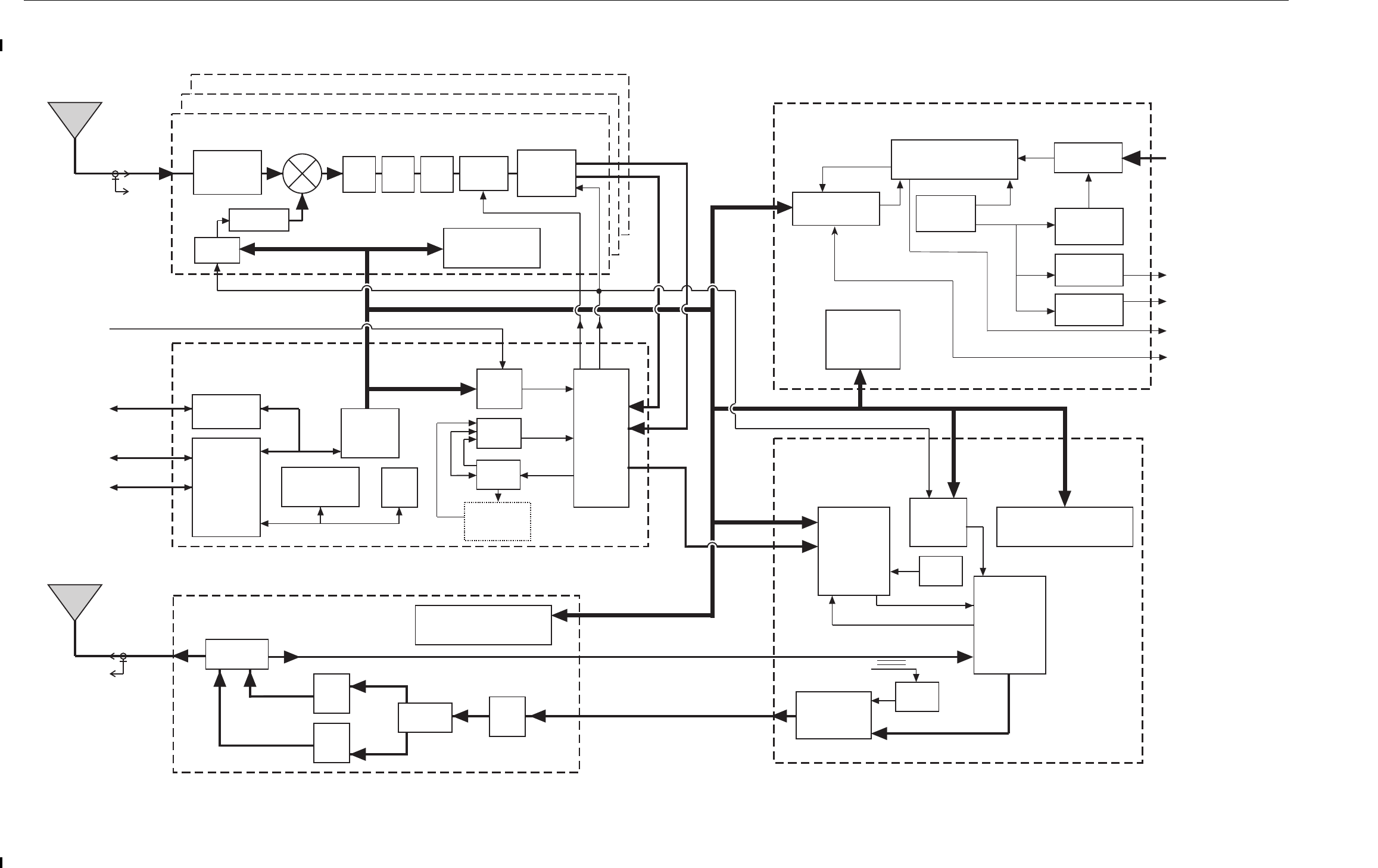
EBTS System Manual - Vol 2 800/900/1500 MHz Base Radios
Base Radio Overview
POWER AMPLIFIER MODULE
TO/FROM
ETHERNET
BASE RADIO CONTROLLER
MODULE
EXCITER MODULE
DC POWER SUPPLY MODULE
SERIAL BUS
TO/FROM
STATUS
PORT
(RS-232)
TO/FROM
RS-232 PORT
(ON BACKPLANE)
16.8 MHZ
5 MHZ
SPI BUS
5 MHZ
EXTERNAL
REFERENCE
FINAL
LINEAR
AMPS SPLITTER LINEAR
DRIVER
ADDRESS DECODE,
MEMORY, A/D CONVERTER
ADDRESS DECODE,
MEMORY, A/D CONVERTER
FROM
RFDS
(RECEIVER
ANTENNA)
#3
3X RECEIVER MODULE
MIXER
DSP BUS
LPF/
PRESELECT/
PREAMP/
IMAGE FILTER
VCO/
SYNTH
ADDRESS DECODE,
MEMORY,
A/D CONVERTER
NON-VOLATILE
MEMORY
(EEPROM,
EPROM)
DRAM
SRAM
HOST
µµ
P
ETHERNET
INTERFACE HOST
GLUE
ASIC
TRANSMIT
DSP
RECEIVE
DSP
SCI
SSI
PLL/
VCO
SPI BUS
2.1 MHZ
COMBINER
LINEAR RF
AMPLIFIER
EXCITER
IC
IF IN IF OUT
TRANLIN
IC
INPUT FILTER
BOARD
CLOCK
GENERATOR
CIRCUITRY START-UP
INVERTER
CIRCUITRY
133 KHZ
267 KHZ
+14.2 V
INVERTER
CIRCUITRY
133 KHZ
DIAGNOSTICS
CIRCUITRY
+14.2 VDC
TO BACKPLANE
+5 VDC
TO BACKPLANE
+28 VDC
TO BACKPLANE
EXTERNAL
DC INPUT
41 - 72 VDC
RF OUT
SPI BUS
SPI BUS
SPI BUS
SPI BUS
2.1 MHZ
SPI BUS
DATA/CLOCK
DATA/CLOCK
RF IN
RF OUT
RF FEEDBACK
FEEDBACK IN
DIGITAL
ATTEN.
CIRCUIT
AGC
SPI BUS
RF IN
CUSTOM
RECEIVER
IC
EBTS284
120497JNM
TO
RFDS
(TRANSMIT
ANTENNA)
MAIN INVERTER
CIRCUITRY
+5 V
INVERTER
CIRCUITRY
TISIC
FROM
RFDS
(RECEIVER
ANTENNA)
#2
MIXER
DSP BUS
LPF/
PRESELECT/
PREAMP/
IMAGE FILTER
RF IN
DIGITAL
ATTEN.
CIRCUIT
CUSTOM
RECEIVER
IC
FROM
RFDS
(RECEIVER
ANTENNA)
#1
MIXER
DSP BUS
LPF/
PRESELECT/
PREAMP/
IMAGE FILTER
RF IN
DIGITAL
ATTEN.
CIRCUIT
CUSTOM
RECEIVER
IC
BAND
PASS
FILTER
BAND
PASS
FILTER
BAND
PASS
FILTER
IF
AMP
IF
AMP
IF
AMP
BAND
PASS
FILTER
BAND
PASS
FILTER
BAND
PASS
FILTER
3-WAY
SPLITTER
NOTES:
1. 2-Branch systems must have a 50Ω load (P/N 5882106P03) installed on Antenna Port #3.
2. Set the RX_FRU_CONFIG parameter as follows:
2-Branch Systems: 12
3-Branch Systems: 123
3. Where two frequencies are given, frequency without parentheses applies to 800 MHz BR only and frequency with parentheses applies to 900 MHz BR only.
970 MHZ
(1025 MHZ)
VCO/SYNTH
FREQUENCY
DOUBLER
237 MHZ
(180.6 MHZ)
VCO
Figure:1-3
800/900 MHz Base Radio Functional Block Diagram
800 MHz And 900 MHz
Base Radio
Functional Block Diagram
1-16
68P81095E02-D 11/9/2000
800/900/1500 MHz Base Radios EBTS System Manual - Vol 2
Base Radio Overview
1500 MHz Base Radio
Functional Block Diagram
POWER AMPLIFIER MODULE
TLN3426
TO/FROM
ETHERNET
BASE RADIO CONTROLLER
MODULE
CLN1469/TLN3425
EXCITER MODULE
TLN3428
POWER SUPPLY MODULE
TLN3429/TLN3339/TLN3338
SERIAL BUS
TRANSMIT
ANTENNA
TO/FROM
SERVICE
COMPUTER
TO/FROM
SYNC MODEM
16.8 MHZ
5 MHZ
SPI BUS
5 MHZ
EXTERNAL
REFERENCE
FINAL
LINEAR
AMP
FINAL
LINEAR
AMP
SPLITTER LINEAR
DRIVER
ADDRESS DECODE,
MEMORY, A/D CONVERTER
ADDRESS DECODE,
MEMORY, A/D CONVERTER
700 MHZ
VCO/SYNTH
FREQUENCY
DOUBLER
RECEIVE
ANTENNA
RECEIVER MODULE
TLN3427
MIXER
DSP BUS
LPF/
PRESELECT/
PERAMP/
IMAGE FILTER
SYNTH/
VCO
BAND
PASS
FILTER
ADDRESS DECODE,
MEMORY,
A/D CONVERTER
NON-VOLATILE
MEMORY
(EEPROM, SRAM,
EPROM)
DRAM
HOST
µ
P
ETHERNET
INTERFACE
HOST
ASIC TRANSMIT
DSP
RECEIVE
DSP
SCI
SSI
PLL/
VCO
SPI BUS
2.1 MHZ
COMBINER
LINEAR RF
AMPLIFIER
AGC
CIRCUIT
EXCITER
IC
IF IN IF OUT
TRANLIN
IC
236 MHZ
VCO
MAIN INVERTER
CIRCUITRY
INPUT FILTER
BOARD
CLOCK
GENERATOR
CIRCUITRY START-UP
INVERTER
CIRCUITRY
133 KHZ
267 KHZ
+14.2 V
INVERTER
CIRCUITRY
+5 V
INVERTER
CIRCUITRY
133 KHZ (TLN3338)
67 KHZ (TLN3429/
TLN3339)
DIAGNOSTICS
CIRCUITRY
+14.2 VDC
TO BACKPLANE
+5 VDC
TO BACKPLANE
+28 VDC
TO BACKPLANE
TO/FROM STORAGE
BATTERY
AC INPUT
47 - 63 HZ
90V/264V
RF OUT
SPI BUS
SPI BUS
SPI BUS
SPI BUS
2.1 MHZ
SPI BUS
DATA/CLOCK
SPI BUS
DATA/CLOCK
RF IN
RF OUT
RF FEEDBACK FEEDBACK IN
ERROR
CORRECTION
DSP
(TLN3425 ONLY)
CORRECTION SIGNALS
2X INJECTION
AMP
DIGITAL
ATTEN.
CIRCUIT
RECEIVER MODULE
RECEIVER MODULE
AGC
SPI BUS
IF
AMP
BAND
PASS
FILTER
RF IN
DSP
GLUE
ASIC
CUSTOM
RECEIVER
IC
Battery Charging/Revert Circuitry is contained only in the TLN3429 and TLN3339 AC Power Supplies.
*
BATTERY CHARGING/
REVERT CIRCUITRY
*
Figure:1-4
1500 MHz Base Radio Functional Block Diagram
1-17
68P81095E02-D 11/9/2000
800/900/1500 MHz Base Radios EBTS System Manual - Vol 2
Base Radio Overview
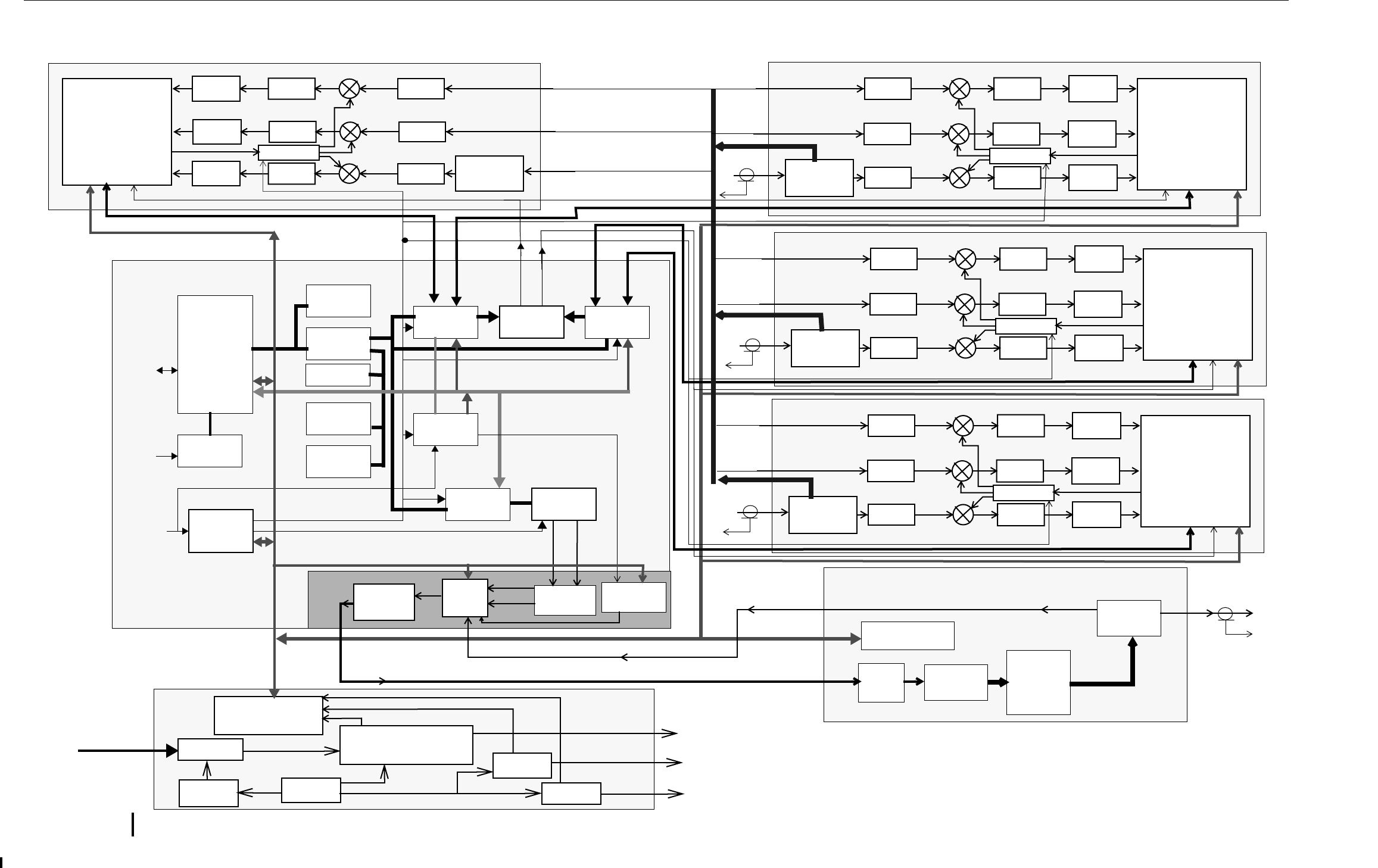
Figure:1-5
800 MHz QUAD Channel Base Radio Functional Block
Diagram
16.8MHz
2.4MHz
48MHz
Host SPI
Host SPI
16.8MHz
STATUS
PORT
RS-232
5 MHZ
EXTERNAL
REFERENCE
ETHERNET
1PPS & SLOT TIMING
RX1 DATA
RX2 DATA
RX3 DATA
RX4 DATA
Rx1&2
Rx3&4
POWER AMPLIFIER MODULE
Tx_I Tx_Q
EXCITER-BASE RADIO
CONTROLLER
HOST
u’P
SDRAM
RECEIVE
DSP
ETHERNET
EEPROM
FLASH
PLL/VCOs
TRANSMIT
DSP
TISIC
TX RECLOCK
BUFFERS
RX SPI
BASE RADIO
CONTROLLER
Exciter
IO LATCHES
RECEIVE
DSP
INTERFACE
ADDRESS DECODE,
MEMORY, ADC
SPI BUS
LINEAR
DRIVER
FINAL
LINEAR
AMPS
COMBINER
SPLITTER
RF OUT
TO RFDS
(TX ANTENNA)
DAC VCOs/Synths
I
Q
ODCT
LINEAR RF
AMPLIFIER
RF IN
RF FEEDBACK
DC POWER SUPPLY MODULE
INPUT FILTER
START-UP
INVERTER
CIRCUITRY
EXTERNAL
DC INPUT
41 - 60 VDC
CLOCK
GENERATOR
133 KHZ 267 KHZ
133 KHZ
14.2 V
CONVERTER
3.3 V
CONVERTER
+28 VDC
TO BACKPLANE
+14.2 VDC
TO BACKPLANE
+3.3 VDC
TO BACKPLANE
Main Converter
MIXER
IF FILTER
AMP, AGC
ABACUS
RECEIVER
IC
LPF, AMP,
FILTER
MIXER
IF FILTER
AMP, AGC
ABACUS
RECEIVER
IC
LPF, AMP,
FILTER
MIXER
IF FILTER
AMP, AGC
ABACUS
RECEIVER
IC
LPF, AMP,
FILTER
RX INTERFACE,
ADDRESS DECODE.
MEMORY, DIAGNOSTICS
PREAMPLIFIER
SPLITTER
/ BYPASS
VCO SYNTH
SPLITTER
RF IN
FROM RFDS
(BRANCH 2)
MIXER
IF FILTER
AMP, AGC
ABACUS
RECEIVER
IC
LPF, AMP,
FILTER
MIXER
IF FILTER
AMP, AGC
ABACUS
RECEIVER
IC
LPF, AMP,
FILTER
MIXER
IF FILTER
AMP, AGC
ABACUS
RECEIVER
IC
LPF, AMP,
FILTER
RX INTERFACE,
ADDRESS DECODE.
MEMORY, DIAGNOSTICS
PREAMPLIFIER
SPLITTER
/ BYPASS
VCO SYNTH
SPLITTER
RF IN
FROM RFDS
(BRANCH 3)
MIXER
IF FILTER
AMP, AGC
ABACUS
RECEIVER
IC
LPF, AMP,
FILTER
MIXER
IF FILTER
AMP, AGC
ABACUS
RECEIVER
IC
LPF, AMP,
FILTER
MIXER
IF FILTER
AMP, AGC
ABACUS
RECEIVER
IC
LPF, AMP,
FILTER
RX INTERFACE,
ADDRESS DECODE.
MEMORY, DIAGNOSTICS
PREAMPLIFIER
SPLITTER
/ BYPASS
VCO SYNTH
SPLITTER
RF IN
FROM RFDS
(BRANCH 1)
RECEIVER 2
RECEIVER 3
RECEIVER 4
RECEIVER 1
MIXER
IF FILTER
AMP, AGC
ABACUS
RECEIVER
IC
LPF, AMP,
FILTER
MIXER
IF FILTER
AMP, AGC
ABACUS
RECEIVER
IC
LPF, AMP,
FILTER
MIXER
IF FILTER
AMP, AGC
ABACUS
RECEIVER
IC
LPF, AMP,
FILTER
RX INTERFACE,
ADDRESS DECODE.
MEMORY, DIAGNOSTICS
PREAMPLIFIER
SPLITTER
/ BYPASS
VCO SYNTH
SPLITTER
SPI BUS
SPI BUS
SPI BUS
ADDRESS DECODE,
MEMORY, ADC
QUAD RX IN DISTRIBUTION
16.8MHz

1-18
68P81095E02-D 11/9/2000
800/900/1500 MHz Base Radios EBTS System Manual - Vol 2
Base Radio Overview

68P81095E02-D 12/6/2000
2-1
EBTS System Manual - Vol 2 800/900/1500 MHz Base Radios
2 Base Radio Controller
Overview
This section provides technical information for the Base Radio Controller (BRC).
Table 2-1 describes covered topics.
FRU Number to Kit Number Cross Reference
Base Radio Controller (BRC) Field Replaceable Units (FRUs) are available for the
iDEN EBTS. The FRU contains the BRC kit and required packaging. Table 2-2
provides a cross reference between BRC FRU numbers and kit numbers.
Table 2-1
Chapter Topics
Chapter Page Description
800/900/1500 MHz Base Radio Controller Ð
CLN1469; 1500 MHz MC1 Base Radio Controller Ð
TLN3425
2-2 Describes the functions and characteristics of the Base Radio
Controller (BRC) module for the single channel Base Radio
(BR).
800 MHz QUAD Channel
Base Radio Controller
2-13 Describes the functions and characteristics of the Base Radio
Controller (BRC) module for the QUAD channel Base Radio
(BR).
Single Channel Base Radio Controller 2-25 Functional Block Diagram for the Single Channel Base Radio
Controller (BRC)
QUAD Channel Base Radio Controller 2-29 Functional Block Diagram for the QUAD Channel Base
Radio Controller (BRC)
Table 2-2
FRU Number to Kit Number Cross Referece
Description FRU Number Kit Number
Single Channel Base Radio Controller
(800/ 900/ 1500 MHz)
TLN3334 CLN1469
Single Channel Base Radio Controller
(1500 MHz MCI)
TLN3425 CLN1472
QUAD Channel Exciter/Base Radio Controller
(800 MHz)
CLN1497 CLF1560

2-2
68P81095E02-D 12/6/2000
800/900/1500 MHz Base Radios EBTS System Manual - Vol 2
800/900/1500 MHz Base Radio Controller – CLN1469; 1500 MHz MC1 Base Radio Controller – TLN3425
800/900/1500 MHz Base Radio Controller – CLN1469;
1500 MHz MC1 Base Radio Controller – TLN3425
Overview
The Base Radio Controller (BRC) provides signal processing and operational
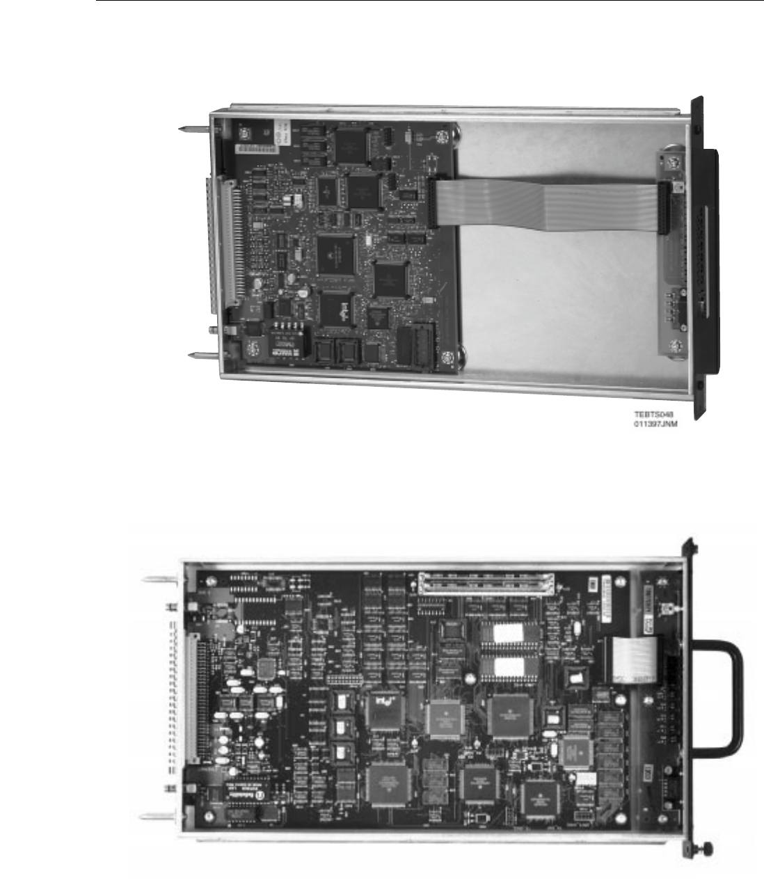
control for other Base Radio modules. Figure 2-1 shows a top view of the BRC
with the cover removed. The BRC module consists of two printed circuit boards
(BRC board and LED/display board), a slide-in housing, and associated
hardware.
The BRC memory contains the operating software and codeplug. The software
deÞnes operating parameters for the BR, such as output power and operating
frequency.
The BRC interconnects to the Base Radio backplane using one 96-pin, DIN
connector and one blindmate, RF connector. Two Torx screws secure the BRC to
the Base Radio chassis.
NOTE
BRC Modules with board level kit number CLN6989
require System Software Release version SR 3.3 or
higher. Using these modules with System Software
versions older than 3.3 causes a PENDULUM lock
error. The Base Radio will not function.
Two BRC modules serve as the main controller for the 1500 MHz Base Radio. The
standard model is the same module that the 800/900 MHz Base Radio uses.
Model TLN3425 contains additional Digital Signal Processing power. This
additional power supports applications that require a modiÞed error correction
routine (available for speciÞc customers only). Figure 2-2 shows a top view of the
BRC (model TLN3425) with the cover removed.
68P81095E02-D 12/6/2000
2-3
EBTS System Manual - Vol 2 800/900/1500 MHz Base Radios
800/900/1500 MHz Base Radio Controller – CLN1469; 1500 MHz MC1 Base Radio Controller – TLN3425
Figure:2-1
Base Radio Controller, version CLN1469 (with cover removed)
1.5GHZ-A859
Figure:2-2
Base Radio Controller, version TLN3425 (with cover removed)
2-4
68P81095E02-D 12/6/2000
800/900/1500 MHz Base Radios EBTS System Manual - Vol 2
800/900/1500 MHz Base Radio Controller – CLN1469; 1500 MHz MC1 Base Radio Controller – TLN3425
Controls and Indicators
The BRC monitors the functions of other Base Radio modules. Front panel LEDs
indicate the status of modules that the BRC monitors. Upon initial power-up, all
front panel LEDs normally ßash three times. A RESET switch allows a manual
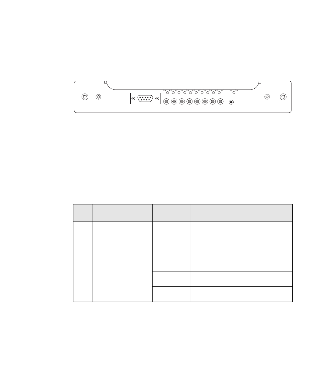
reset of the Base Radio. Figure 2-3 shows the BRC front panel.
Indicators
Table 2-3 lists and describes the BRC LEDs.
Table 2-3
BR Controller Indicators
LED Color Module
Monitored Condition Indications
BR Green BR Solid (on) Station is keyed
Flashing (on) Station is not keyed
Off Station is out of service or power is
removed
PS Red Power
Supply
Solid (on) FRU failure indication - Power Supply has
a major alarm, and is out of service
Flashing (on) Power Supply has a minor alarm, and may
be operating at reduced performance
Off Power Supply is operating normally (no
alarms)
EBTS316
122796JNM
CONTROL
RESETBR PS EX PA CTL R1 R2 R3
STATUS
Figure:2-3
BR Controller (Front View)

68P81095E02-D 12/6/2000
2-5
EBTS System Manual - Vol 2 800/900/1500 MHz Base Radios
800/900/1500 MHz Base Radio Controller – CLN1469; 1500 MHz MC1 Base Radio Controller – TLN3425
Controls
Table 2-4 lists the controls and descriptions.
STATUS Connector
Table 2-5 the pin-outs for the STATUS connector.
EX Red Exciter Solid (on) FRU failure indication - Exciter has a major
alarm, and is out of service
Flashing (on) Exciter has a minor alarm, and may be
operating at reduced performance
Off Exciter is operating normally
(no alarms)
PA Red Power
AmpliÞer
Solid (on) FRU failure indication - PA has a major
alarm, and is out of service
Flashing (on) PA has a minor alarm and may be
operating at reduced performance
Off PA is operating normally (no alarms)
CTL Red Controller Solid (on) FRU failure indication - BRC has a major
alarm, and is out of service
Flashing (on) BRC has a minor alarm, and may be
operating at reduced performance
Off BRC is operating normally (no alarms)
R1
R2
R3
Red Receiver #1,
#2, or #3
Solid (on) FRU failure indication - Receiver (#1, #2,
or #3) has a major alarm, and is out of
service
Flashing (on) Receiver (#1, #2, or #3) has a minor alarm,
and may be operating at reduced
performance
Off Receiver (#1, #2, or #3) is operating
normally (no alarms)
Table 2-4
BR Controller Controls
Control Description
RESET Switch A push-button switch used to manually reset the BR.
STATUS
connector
A 9-pin connector used for connection of a service computer. Provides a
convenient means for testing and conÞguring.
Table 2-3
BR Controller Indicators (Continued)
LED Color Module
Monitored Condition Indications

2-6
68P81095E02-D 12/6/2000
800/900/1500 MHz Base Radios EBTS System Manual - Vol 2
800/900/1500 MHz Base Radio Controller – CLN1469; 1500 MHz MC1 Base Radio Controller – TLN3425
Theory of Operation
Table 2-6 brießy describes the BRC circuitry. Figures 2-6 and 2-7 are functional
block diagrams of the Single Channel BRC.
Table 2-5
Pin-outs for the STATUS Connector
Pin-out Signal
1CD
2 TXD
3 RXD
4 not used
5 GND
6 not used
7 CTS
8RTS
9 not used
Table 2-6
BR Controller Circuitry
Circuit Description
Host Microprocessor and
Host Glue ASIC
Contains two integrated circuits that comprise the central
controller of the BRC and station.
Non-Volatile Memory Consists of:
¥ EPROMs containing the station operating software
¥ one EEPROM containing the station codeplug data
Volatile Memory Contains DRAM to store station software that executes
commands. Contains SRAM which the host microprocessor
uses for general data space.
Ethernet Interface Provides the BRC with a 10Base2 Ethernet communication port.
The interface networks both control and compressed voice
data.
RS-232 Interface Provides the BRC with two independent RS-232 serial
interfaces.
Digital Signal Processors and
TISIC
Performs high-speed modulation/demodulation of
compressed audio and signaling data.
Station Reference Circuitry Generates the 16.8 MHz and 2.1 MHz reference signal used
throughout the station.
Input Ports Contains two 16-line input buses. These buses receive
miscellaneous inputs from the BR.
Output Ports Contains three 16-line output buses. These buses provide a path
for sending miscellaneous control signals to circuits throughout
the BR.
Remote Station Shutdown Provides software control to cycle power on the BR.

68P81095E02-D 12/6/2000
2-7
EBTS System Manual - Vol 2 800/900/1500 MHz Base Radios
800/900/1500 MHz Base Radio Controller – CLN1469; 1500 MHz MC1 Base Radio Controller – TLN3425
Host Microprocessor
The host microprocessor is the the BRÕs main controller. The host operates at a
clock speed of 16.5 MHz. The Host Glue ASIC provides this clock frequency. The
processor controls Base Radio operation according to station software in
non-volatile memory. Two EPROMs contain the station software. An EEPROM
stores the station codeplug.
Serial Communication Buses
The microprocessor provides a general-purpose SCC2 serial communications bus.
The SCC2 serial communications bus is an asynchronous RS-232 interface. The
the BRC front panel includes a 9-pin, D-type
connector. This connector provides a
port where service personnel may connect a service computer. The service
computer allows downloading of application code or diagnostic software. Service
personnel can perform programming and maintenance tasks via Man Machine
Interface (MMI) commands. The interface between the SCC2 port and the front
panel STATUS connector is via EIA-232 Bus Receivers/Drivers.
Address and Data Bus
The microprocessor has a 23-line address bus. The processor uses this bus to
access non-volatile and DRAM memory. The processor also uses the bus to
provide control for other BRC circuitry via memory mapping.
A 16-line data bus transfers data to and from the BRC memory. Such bus transfers
may involve other BRC circuitry, too. Buffers on the data bus allow transfers to
and from non-volatile and DRAM memory.
Host Glue ASIC
The Host Microprocessor controls the operations of the Host Glue ASIC. Table 2-7
describes this ASICÕs functions.
Table 2-7
Host Glue ASIC Functions
Function Description
SPI Bus Serves as a general-purpose, serial communications bus. Provides
communications between the Host Microprocessor and other Base
Radio modules.
DRAM Controller Provides signals necessary to access and refresh DRAM memory.
System Reset Generates a BRC Reset at power-up.
Host Microprocessor
Clock
Buffers the 33 MHz crystal outputs. Performs a divide-by-2 operation.
Outputs a 16.5 MHz clock signal for the Host Microprocessor.
Address Decoding Decodes addresses from the Host Microprocessor. Generates
corresponding chip-select signals for various BRC devices, such as:
DRAM, EPROM, I/O Ports, DSPs, and internal Host Glue ASIC
registers.
Interrupt Controller Accepts interrupt signals from various BRC circuits (such as the DSPs).
Organizes the interrupts based on hardware-deÞned priority ranking.
Sends interrupt and priority level information to the Host
Microprocessor (via IPL lines 1-3).

2-8
68P81095E02-D 12/6/2000
800/900/1500 MHz Base Radios EBTS System Manual - Vol 2
800/900/1500 MHz Base Radio Controller – CLN1469; 1500 MHz MC1 Base Radio Controller – TLN3425
Non-Volatile Memory
The Base Radio software resides in two 512K x 8 byte EPROMs. The Host
Microprocessor addresses these EPROMs via 19 of 23 host address bus lines. The
host accesses EPROM data over the 16-line host data bus.
The data that determines the station personality resides in an 8K x 8 byte
codeplug EEPROM. The microprocessor addresses the EEPROM over 15 of 23
host address bus lines. The host accesses EEPROM data over the 16-line data bus.
Stations ship with default data programmed into the codeplug. The BRC must
download Þeld programming information from network and site controllers. This
data includes operating frequencies and output power level. The station permits
adjustment of many station parameters, but the station does not store
adjustments. Refer to this manualÕs Software Commands chapter for additional
information.
Volatile Memory
Each BRC contains 2MB of DRAM. The BRC downloads station software code
into DRAM for station use. Since DRAM is volatile memory, it loses data during a
system reset or power failure.
DRAM also provides short-term storage for data generated and required during
normal operation. The BRC performs read and write operations over the Host
Address and Data buses. Read and write operations also involve column and row
select lines. The Host Glue ASIC controls these lines. The Host Glue ASIC also
controls address bus and column row signals. During normal operation, the
address bus and column row signals sequentially refresh DRAM memory
locations.
The BRC also includes two 32K x 8 byte fast Static RAM (SRAM) ICs. The
microprocessor accesses SRAM over the Data Bus and Host Address Bus. Access
requires the entire Data Bus, and 15 of the Host Address BusÕ 23 lines.
Ethernet Interface
The Ethernet Interface includes a Local Area Network (LAN) Controller. This
LAN Controller is a 32-bit address, 16-bit data LAN coprocessor. The LAN
coprocessor implements the CSMA/CD access method, which supports the IEEE
802.3 10Base2 standard. The LAN coprocessor communicates with the Host
Microprocessor via DRAM. The LAN coprocessor uses 22 of its 32 address lines
for the Ethernet interface.
The LAN coprocessor supports all IEEE 802.3 Medium Access Control, including
the following:
❐
framing
❐
preamble generation
❐
stripping
❐
source address generation
❐
destination address checking

68P81095E02-D 12/6/2000
2-9
EBTS System Manual - Vol 2 800/900/1500 MHz Base Radios
800/900/1500 MHz Base Radio Controller – CLN1469; 1500 MHz MC1 Base Radio Controller – TLN3425
The LAN coprocessor receives commands from the CPU by reading a speciÞed
memory block. The LAN ControllerÕs internal FIFOs optimize microprocessor bus
performance.
The LAN coprocessor includes an on-chip, Direct Memory Access (DMA)
controller. The DMA controller automatically transfers data blocks (buffers and
frames) from Ethernet to DRAM. These automatic data transfers relieve the host
CPU of byte transfer overhead.
The Ethernet Serial Interface works with the LAN coprocessor to perform these
major functions:
❐
10 MHz transmit clock generation (obtained by dividing the 20 MHz signal
provided by an on-board crystal)
❐
Manchester encoding and decoding of frames
❐
electrical interface to the Ethernet transceiver
An isolation transformer provides high voltage protection. The transformer also
isolates the Ethernet Serial Interface (ESI) and the transceiver. The pulse
transformer has the following characteristics:
❐
Minimum inductance of 75
µ
H
❐
2000 V isolation between primary and secondary windings
❐
1:1 Pulse Transformer
The Coaxial Transceiver Interface (CTI) is a coaxial cable line driver/receiver for
the Ethernet. CTI provides a 10Base2 connection via a coaxial connector on the
board. This device minimizes the number of external components necessary for
Ethernet operations.
A DC/DC converter provides a constant voltage of -9 Vdc for the CTI. The
converterÕs input source voltage is 5 Vdc.
The CTI performs the following functions:
❐
Receives and transmits data to the Ethernet coaxial connection
❐
Reports any collision that it detects on the coaxial connection
❐
Disables the transmitter when packets are longer than the legal length
(Jabber Timer)
Digital Signal Processors
The BRC includes a Receive Digital Signal Processor (RXDSP) and a Transmit
Digital Signal Processor (TXDSP). These DSPs and related circuitry process
compressed station transmit and receive audio or data. The related circuitry
includes the TDMA Infrastructure Support IC (TISIC) and the TISIC Interface
Circuitry. The DSPs only accepts input and output signals in digitized form.
The inputs are digitized receiver signals. The outputs are digitized voice audio
and data (modulation signals). The output DSP sends these signals to the Exciter.
DSPs communicate with the Microprocessor via an 8-bit host data bus. This bus is
on the Host Processor side. For all DSPs, interrupts drive communication.

2-10
68P81095E02-D 12/6/2000
800/900/1500 MHz Base Radios EBTS System Manual - Vol 2
800/900/1500 MHz Base Radio Controller – CLN1469; 1500 MHz MC1 Base Radio Controller – TLN3425
The RXDSP operates from a 40 MHz clock provided by an on-board crystal. The
RXDSP accepts redigitized signal from the receivers. The
RXDSP also provides
address and data buses. These buses receive digitized audio from the TISIC.
The DSP program and signal processing algorithms reside in three 32K x 8 SRAM
ICs. The RXDSP accesses this software there. The RXDSP communicates with the
host bus via an 8-bit interface.
The Synchronous Serial Interface (SSI) port offers a serial data path to the TXDSP.
The Serial Communications Interface (SCI) port provides a serial control path
from the TXDSP.
The TXDSP operates at a clock speed of 40 MHz, provided by a clock oscillator.
The TXDSP sends the digitized signal to the TISIC. The TSCI then passes the
signal to the Exciter.
The TXDSP contains its own address and data buses. It uses these buses to access
its DSP program and signal processing algorithms in local memory. The TXDSP
memory consists of six 32K x 8 SRAM ICs. The TXDSP communicates with the
host bus via an 8-bit interface.
Error Correction Digital Signal Processor
(
TLN3425 Only)
The Error Correction Digital Signal Processor
(U30) in the Model TLN3425A
operates at a clock speed of 60 MHz. An on-board
oscillator (Y100) operates at 10
MHz. Circuitry inside the ECDSP multiplies this frequency to generate the
required clock signal.
Decoding is the main function of the Error Correction Digital Signal Processor
(ECDSP). The ECDSP accepts data from the Synchronous Serial Interface (SSI)
bus. The ECDSP performs various algorithms on the signal. Then the signal enters
the TXDSP via the SSI bus.
The ECDSP contains its own address and data buses. It uses these buses to access
its DSP program and signal processing algorithms in local memory. Two 32K x 8
SRAM ICs (U27 and U31) comprise the ECDSP memory. The ECDSP
communicates with the host bus via an 8-bit interface.

68P81095E02-D 12/6/2000
2-11
EBTS System Manual - Vol 2 800/900/1500 MHz Base Radios
800/900/1500 MHz Base Radio Controller – CLN1469; 1500 MHz MC1 Base Radio Controller – TLN3425
TISIC
The TISIC controls internal DSP operations. This circuit provides a number of
functions, including the following:
❐
Interfaces with the DSPs via the DSP address and data buses.
❐Accepts a 16.8 MHz signal and a 1 PPS signal from Station
Reference Circuitry.
❐Outputs a 2.1 MHz reference signal used by the Exciter and Receivers.
❐Outputs a 4.8 MHz reference signal used by the Exciter to clock data into the
TRANLIN IC.
❐Accepts differential data from the Receiver (RX1 through RX3) via
interface circuitry.
❐Accepts and sends serial data from the Receiver (RX1 through RX3) via the
serial data bus.
❐Accepts and formats differential data from the TXDSP for transmission to
the Exciter via interface circuitry.
❐Generates 15 ms and 7.5 ms ticks. These synchronize to the 1 PPS time mark
from the iSC. The system routes these ticks to the TXDSP and RXDSP,
respectively.
❐Generates the Receive SSI (RXSSI) frame sync interrupt for the RXDSP.
Station Reference Circuitry
The Station Reference Circuitry is a phase-locked loop (PLL). This PLL consists of
a high-stability, Voltage Controlled Crystal Oscillator (VCXO) and a Phase Locked
Loop IC. The iSCÕs GPS output connects to the 5 MHz/1 PPS A BNC connector on
the EBTS junction panel.
The PLL compares the reference frequency to the 16.8 MHz VCXO output. The
PLL then generates a DC correction or control voltage. With the control voltage
enable switch closed, the PLLÕs control voltage adjusts the VCXO frequency. This
adjustment achieves a stability equivalent to that of the external 5 MHz frequency
reference.
The control voltage from the PLL continuously frequency-controls the VXCO. The
VXCO outputs a 16.8 MHz clock signal, and applies the signal to the TISIC.
The TISIC divides the 16.8 MHz signal by eight and outputs a 2.1 MHz signal. A
splitter separates and buffers this signal. Then via the backplane, the output
signal enters the Exciter and Receivers as a 2.1 MHz reference .
The 4.8 MHz reference signal generated by the TISIC enters the Exciter module.
There it clocks data into and out of the TRANLIN IC.

2-12 68P81095E02-D 12/6/2000
800/900/1500 MHz Base Radios EBTS System Manual - Vol 2
800/900/1500 MHz Base Radio Controller – CLN1469; 1500 MHz MC1 Base Radio Controller – TLN3425
Input Ports
Two general purpose, 16-line input ports provide for various input signals from
the BRC and station circuitry. These inputs connect to the Host Microprocessor.
Input Port P0 -In and Port P1-In each consist of 16 lines. Via the backplane, these
lines carry signals from BRC circuitry and other station modules. The buses
communicate with the buffers to make data available to the Host Microprocessor
via the Host Data Bus. The DIP switch and Station Reference Circuitry are typical
inputs for these ports.
Output Ports
Three general purpose, 16-line output ports provide various control signals from
the Host Microprocessor. Via the backplane, these output ports carry control
signals to the BRC and station circuitry.
Output ports P0-Out through Port P2-Out each consist of 16 lines. These lines
derive from the Host Data Bus via latches.
Typical control signals include front panel LED control signals and SPI peripheral
address select lines.
Remote Station Shutdown
BRC circuitry can send a shutdown pulse to the Base Radio Power Supply. After
receiving this pulse, the power supply cycles BR power. The shutdown affects 5.1
Vdc, 28.6 Vdc and 14.2 Vdc sources. The BRC produces the shutdown pulse by
invoking software control signals. A remote site uses the shutdown function to
perform a hard reset of all BR modules.
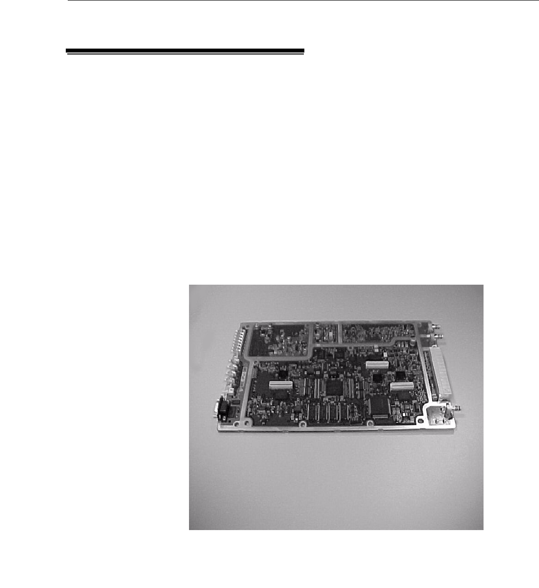
68P81095E02-D 12/6/2000 2-13
EBTS System Manual - Vol 2 800/900/1500 MHz Base Radios
800 MHz QUAD Channel Base Radio Controller
800 MHz QUAD Channel Base Radio Controller
Overview
The Base Radio Controller (BRC) provides signal processing and operational
control for Base Radio modules. The BRC module consists of a printed circuit
board, a slide-in housing, and associated hardware.
The BRC memory contains the operating software and codeplug. The software
deÞnes BR operating parameters, such as output power and operating frequency.
The BRC connects to the Base Radio backplane with one 168-pin FutureBus+
connector and one blindmate RF connector. Two Torx screws secure the BRC in
the Base Radio chassis.
Figure 2-4 shows a top view of the BRC (model CLF6290A) with the cover
removed.
Controls and Indicators
The BRC monitors the functions of other Base Radio modules. The LEDs on the
front panel indicate the status of BRC-monitored modules. All LEDs on the BRC
front panel normally ßash three times upon initial power-up. A RESET switch
Figure:2-4
Base Radio Controller, version CLN1469 (with cover removed)
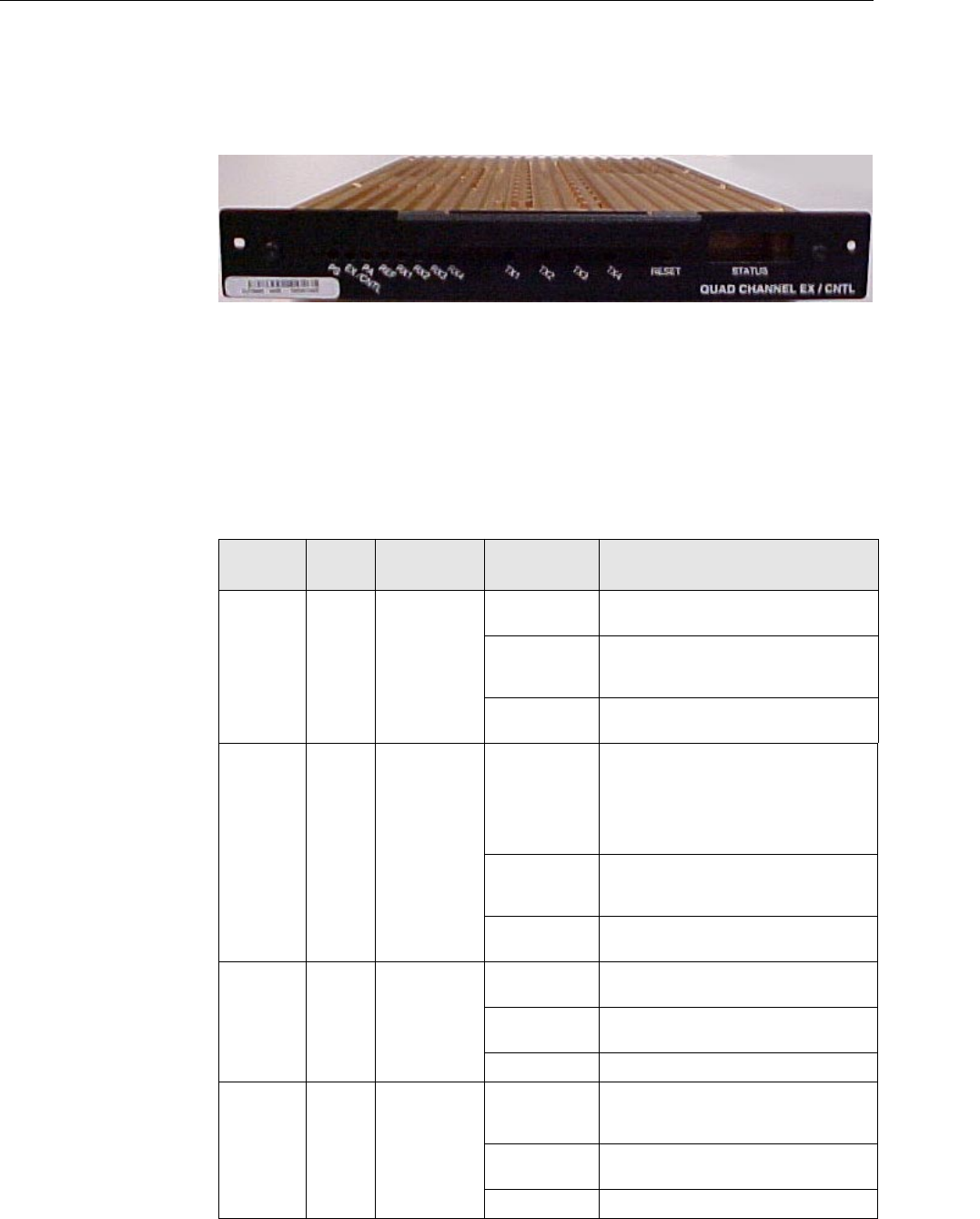
2-14 68P81095E02-D 12/6/2000
800/900/1500 MHz Base Radios EBTS System Manual - Vol 2
800 MHz QUAD Channel Base Radio Controller
allows a manual reset of the Base Radio. Figure 2-5 shows the front panel of the
BRC.
Indicators
Table 2-8 lists and describes the BRC LEDs.
Table 2-8
BR Controller Indicators
LED Color Module
Monitored Condition Indications
PS Red Power
Supply
Solid (on) FRU failure indication - Power Supply
has a major alarm, and is out of service
Flashing (on) Power Supply has a minor alarm, and
may be operating at reduced
performance
Off Power Supply is operating normally
(no alarms)
EXBRC Red Controller/
Exciter
Solid (on) FRU failure indication - Controller/
Exciter has a major alarm, and is out of
service (Note: Upon power-up of the
BR, this LED indicates a failed mode
until BR software achieves a known
state of operation.)
Flashing (on) Controller/Exciter has a minor alarm,
and may be operating at reduced
performance
Off Controller/Exciter is operating
normally (no alarms)
PA Red Power
AmpliÞer
Solid (on) FRU failure indication - PA has a major
alarm, and is out of service
Flashing (on) PA has a minor alarm, and may be
operating at reduced performance
Off PA is operating normally (no alarms)
REF Red Controller
Station
Reference
Solid (on) FRU failure indication - Controller
Station Reference has a major alarm,
and is out of service
Flashing (on) BRC has a minor alarm, and may be
operating in a marginal region
Off BRC is operating normally (no alarms)
Figure:2-5
BR Controller (Front View)

68P81095E02-D 12/6/2000 2-15
EBTS System Manual - Vol 2 800/900/1500 MHz Base Radios
800 MHz QUAD Channel Base Radio Controller
Controls
Table 2-9 lists the controls and descriptions.
STATUS Connector
Table 2-10 the pin-outs for the STATUS connector.
RX1
RX2
RX3
RX4
Red Receiver #1,
#2, #3, or #4
Solid (on) FRU failure indication - Receiver (#1,
#2, #3 or #4) has a major alarm, and is
out of service
Flashing (on) Receiver (#1, #2, #3 or #4) has a minor
alarm, and may be operating at
reduced performance
Off Receiver (#1, #2, #3 or #4) is operating
normally (no alarms)
TX1 Green BR Solid (on) Station Transmit Carrier #1 is keyed
Flashing (on) Station Transmit Carrier #1 is not
keyed
Off Station is out of service, or power is
removed
TX2 Green BR Solid (on) Station Transmit Carrier #2 is keyed
Flashing (on) Station Transmit Carrier #2 is not
keyed
Off Station is out of service, or power is
removed
TX3 Green BR Solid (on) Station Transmit Carrier #3 is keyed
Flashing (on) Station Transmit Carrier #3 is not
keyed
Off Station is out of service, or power is
removed
TX4 Green BR Solid (on) Station Transmit Carrier #4 is keyed
Flashing (on) Station Transmit Carrier #4 is not
keyed
Off Station is out of service, or power is
removed
Table 2-9
BR Controller Controls
Control Description
RESET Switch A push-button switch used to manually reset the BR.
STATUS
connector
A 9-pin connector used for connection of a service computer, providing a
convenient means for testing and conÞguring.
Table 2-8
BR Controller Indicators (Continued)
LED Color Module
Monitored Condition Indications

2-16 68P81095E02-D 12/6/2000
800/900/1500 MHz Base Radios EBTS System Manual - Vol 2
800 MHz QUAD Channel Base Radio Controller
Theory of Operation
Table 2-11 brießy describes the BRC circuitry. Figure 2-9 is a functional block
diagram of the BRC.
Table 2-10
Pin-outs for the STATUS Connector
Pin-out Signal
1 not used
2 TXD
3 RXD
4 not used
5 GND
6 not used
7 not used
8 not used
9 not used
Table 2-11
BR Controller Circuitry
Circuit Description
Host Microprocessor Contains integrated circuits that comprise the central controller
of the BRC and station
Non-Volatile Memory Consists of:
¥ FLASH containing the station operating software
¥ EEPROM containing the station codeplug data
Volatile Memory Contains SDRAM to store station software used to execute
commands.

68P81095E02-D 12/6/2000 2-17
EBTS System Manual - Vol 2 800/900/1500 MHz Base Radios
800 MHz QUAD Channel Base Radio Controller
Host Microprocessor
The host microprocessor is the main controller for the BR. The processor operates
at a 50-MHz clock speed. The processor controls Base Radio operation according
to station software in memory. Station software resides in FLASH memory. For
normal operation, the system transfers this software to non-volatile memory. An
EEPROM contains the station codeplug.
NOTE
At BR power-up, the EXBRC LED indicates a major
alarm. This indication continues until BR software
achieves a predetermined state of operation.
Afterward, the software turns off the EXBRC LED.
Serial Communication Buses
The microprocessor provides a general-purpose SMC serial management
controller bus.
The SMC serial communications bus is an asynchronous RS-232 interface with no
hardware handshake capability. The BRC front panel includes a nine-pin, D-type
connector. This connector provides a port where service personnel may connect a
service computer. Service personnel can perform programming and maintenance
tasks via Man-Machine Interface (MMI) commands. The interface between the
Ethernet Interface Provides the BRC with a 10Base2 Ethernet communication port
to network both control and compressed voice data
RS-232 Interface Provides the BRC with an RS-232 serial interface
Digital Signal Processors Performs high-speed modulation/demodulation of
compressed audio and signaling data
TISIC Contains integrated circuits that provide timing reference
signals for the station
TX Reclock Contains integrated circuits that provide highly stable,
reclocked transmit signals and peripheral transmit logic
RX DSP SPI Contains integrated circuits that provide DSP SPI capability
and peripheral transmit logic
Station Reference Circuitry Generates the 16.8 MHz and 48 MHz reference signals used
throughout the station
Input Ports Contains 16 signal input ports that receive miscellaneous
inputs from the BR
Output Ports Contains 40 signal output ports, providing a path for sending
miscellaneous control signals to circuits throughout the BR
Remote Station Shutdown Provides software control to cycle power on the BR
Table 2-11
BR Controller Circuitry
Circuit Description

2-18 68P81095E02-D 12/6/2000
800/900/1500 MHz Base Radios EBTS System Manual - Vol 2
800 MHz QUAD Channel Base Radio Controller
SMC port and the front- panel STATUS connector is via EIA-232 Bus Receivers
and Drivers.
Host Processor
The microprocessor incorporates 4k bytes of instruction cache and 4k bytes of
data cache that signiÞcantly enhance processor performance.
The microprocessor has a 32-line address bus. The processor uses this bus to
access non-volatile memory and SDRAM memory. Via memory mapping, the
processor also uses this bus to control other BRC circuitry.
The microprocessor uses its Chip Select capability to decode addresses and assert
an output signal. The eight chip-select signals select non-volatile memory,
SDRAM memory, input ports, output ports, and DSPs.
The Host SPI serves as a general-purpose, serial communications bus. This bus...
❐Provides communications between the Host Microprocessor and other Base
Radio modules.
❐Provides condition signals necessary to access SDRAM, FLASH, and DSP.
❐Provides refresh capability to SDRAM memory.
❐Accepts interrupt signals from BRC circuits (such as DSPs).
❐Organizes the interrupts, based on hardware-deÞned priority ranking.
The Host supports several internal interrupts from its Communications Processor
Module. These interrupts allow efÞcient use of peripheral interfaces.
The Host supports 10 Mbps Ethernet/IEEE 802.3.
A 32-line data bus transfers data to and from BRC memory and other BRC
circuitry. Buffers on this data bus allow transfers to and from non-volatile and
SDRAM memory.
Non-Volatile Memory
Base Radio software resides in 2M x 32 bytes of FLASH memory. The Host
Microprocessor addresses the FLASH memory with 20 of the host address busÕ 32
lines. The host accesses FLASH data over the 32-line host data bus. A
host-operated chip-select line provides control signals for these transactions.
The FLASH contains the operating system and application code. The system
stores application code in FLASH for fast recovery from reset conditions.
Application code transfers from network or site controllers may occur in a
background mode. Background mode transfers allow the station to remain
operational during new code upgrades.
The data that determines the station personality resides in a 32K x eight byte
codeplug EEPROM. The microprocessor addresses the EEPROM with 15 of the
host address busÕ 32 lines. The host accesses EEPROM data with eight of the data
busÕ 32 lines. A host-operated chip-select line provides control signals for these
transactions.

68P81095E02-D 12/6/2000 2-19
EBTS System Manual - Vol 2 800/900/1500 MHz Base Radios
800 MHz QUAD Channel Base Radio Controller
During the manufacturing process, the factory programs the codeplugÕs default
data. The BRC must download Þeld programming data from network and site
controllers. This data includes operating frequencies and output power level. The
station permits adjustment of many station parameters, but the station does not
store these adjustments. Refer to the Software Commands chapter for additional
information.
Volatile Memory
Each BRC contains 8MB x 32 bytes of SDRAM. The BRC downloads station
software code into SDRAM for station use. SDRAM also provides short-term
storage for data generated and required during normal operation. SDRAM is
volatile memory. A loss of power or system reset destroys SDRAM data.
The system performs read and write operations over the Host Address and Data
buses. These operations involve column and row select lines under control of the
Host processorÕs DRAM controller. The Host Glue ASICÕs address bus and
column row signals sequentially refresh SDRAM memory locations.
Ethernet Interface
The Host processorÕs Communications Processor Module (CPM) provides the
Local Area Network (LAN) Controller for the Ethernet Interface. The LAN
function implements the CSMA/CD access method, which supports the IEEE
802.3 10Base2 standard.
The LAN coprocessor supports all IEEE 802.3 Medium Access Control, including
the following:
❐framing
❐preamble generation
❐stripping
❐source address generation
❐destination address checking
The PCM LAN receives commands from the CPU.
The Ethernet Serial Interface works directly with the CPM LAN to perform the
following major functions:
❐10 MHz transmit clock generation (obtained by dividing the 20 MHz signal
provided by on-board crystal)
❐Manchester encoding/decoding of frames
❐electrical interface to the Ethernet transceiver
An isolation transformer provides high-voltage protection. The transformer also
isolates the Ethernet Serial Interface (ESI) and the transceiver. The pulse
transformer has the following characteristics:
❐Minimum inductance of 75 µH
❐2000 V isolation between primary and secondary windings
❐1:1 Pulse Transformer

2-20 68P81095E02-D 12/6/2000
800/900/1500 MHz Base Radios EBTS System Manual - Vol 2
800 MHz QUAD Channel Base Radio Controller
The Coaxial Transceiver Interface (CTI) is a coaxial cable line driver and receiver
for the Ethernet. CTI provides a 10Base2 connection via a coaxial connector on the
board. This device minimizes the number of external components necessary for
Ethernet operations.
A DC/DC converter provides a constant voltage of -9 Vdc for the CTI from a
3.3 Vdc source.
The CTI performs the following functions:
❐Receives and transmits data to the Ethernet coaxial connection
❐Reports any collision that it detects on the coaxial connection
❐Disables the transmitter when packets are longer than the legal length
(Jabber Timer)
Digital Signal Processors
The BRC includes two Receive Digital Signal Processors (RXDSPs) and a Transmit
Digital Signal Processor (TXDSP). These DSPs and related circuitry process
compressed station transmit and receive audio or data. The related circuitry
includes the TDMA Infrastructure Support IC (TISIC) and the TISIC Interface
Circuitry. The DSPs only accept input and output signals in digitized form.
The inputs are digitized receiver signals. The outputs are digitized voice audio
and data (modulation signals). These signals pass from the DSP to the Exciter
portion of the EXBRC. DSPs communicate with the Microprocessor via an
eight-bit, host data bus on the host processor side. For all DSPs, interrupts drive
communication with the host.
The RXDSPs operate from an external 16.8 MHz clock, provided by the local
station reference. The RXDSP internal operating clock signal is 150MHz,
produced by an internal Phase-Locked Loop (PLL).
The RXDSPs accept digitized signals from the receivers through Enhanced
Synchronous Serial Interface (ESSI) ports. Each of two ESSI ports on a RXDSP
supports a single carrier (single receiver) digital data input. The DSP circuitry
includes two RXDSPs. These allow processing of up to four carriers (four
receivers).
The RXDSP accesses its DSP program and signal-processing algorithms in 128k
words of internal memory. The RXDSPs communicate with the host bus over an
8-bit interface.
Each RXDSP provides serial communications to its respective receiver module for
receiver control via a Serial Peripheral Interface (SPI). The SPI is a
parallel-to-serial conversion circuit, connected to the RXDSP data bus. Each
RXDSP communicates to two receive modules through this interface.
Additionally, a serial control path connects the two RXDSPs and the TXDSP. The
Synchronous Communications Interface (SCI) port facilitates this serial control
path.
For initialization and control purposes, one RXDSP connects to the TISIC device.

68P81095E02-D 12/6/2000 2-21
EBTS System Manual - Vol 2 800/900/1500 MHz Base Radios
800 MHz QUAD Channel Base Radio Controller
The TXDSP operates at an external clock speed of 16.8 MHz, provided by the
EXBRC local station reference. The TXDSP internal operating clock is 150MHz,
produced by an internal Phase Lock Loop (PLL).
The TXDSP sends up to four carriers of digitized signal to the EX11 exciter. The
exciter converts the digital signal to analog. Also at the exciter, a highly stable
clock reclocks the digital data. Reclocking enhances transmit signal integrity. Two
framed and synchronized data streams result. One data stream is I-data, and the
other is the Q-data stream.
The TXDSP contains its own, internal address and data memory. The TXDSP can
store 128k words of DSP program and data memory. An eight-bit interface
handles TXDSP-to-host bus communications.

2-22 68P81095E02-D 12/6/2000
800/900/1500 MHz Base Radios EBTS System Manual - Vol 2
800 MHz QUAD Channel Base Radio Controller
TISIC
The TISIC controls internal DSP operations. This circuit provides the following
functions:
❐For initialization and control, interfaces with one RXDSP via the DSP
address and data buses.
❐Accepts a 16.8 MHz signal from Station Reference Circuitry.
❐Accepts a 5 MHz signal, modulated with one pulse per second (1 PPS) from
the site reference.
❐Demodulates the 1 PPS
❐Outputs a 1 PPS signal and a windowed version of this signal for network
timing alignment.
❐Outputs a 2.4 MHz reference signal used by the Exciter.l
❐Generates 15 ms and 7.5 ms ticks. (These ticks synchronize to the 1 PPS time
mark. The system decodes the time mark from the site reference. Then the
system routes the reference to the TXDSP and RXDSPs.)
Station Reference Circuitry
The Station Reference Circuitry is a phase-locked loop (PLL). This PLL consists of
a high-stability, Voltage-Controlled, Crystal Oscillator (VCXO) and a PLL IC. GPS
output from the iSC connects to the 5 MHz/1 PPS BNC connector on the BR
backplane. Wiring at this connector routes signals to EXBRC station reference
circuitry.
The PLL compares the 5 MHz reference frequency to the 16.8 MHz VCXO output.
Then the PLL generates a DC correction voltage. The PLL applies this correction
voltage to the VCO through an analog gate. The analog gate closes when three
conditions coexist: (1) The 5 MHz tests stable. (2) The PLL IC is programmed. (3)
Two PLL oscillator and reference signal output alignments occur.
A loss of the 5 MHz / 1 PPS signal causes the control voltage enable switch to
open. This complex PLL control allows the BR to maintain call-handover
capability during short disconnects (approximately one minute) of the 5 MHz/1
PPS signal. (For example, during 5 MHz/1 PPS cable maintenance work.)
When the gate enables, the control voltage from the PLL can adjust the
high-stability VCXO frequency. The adjustment can achieve a stability nearly
equivalent to that of the external, 5 MHz frequency reference.
The correction voltage from the PLL continuously adjusts the VXCO frequency.
The VXCO outputs a 16.8 MHz clock signal. The circuit applies this clock signal to
the receiver, 48 MHz reference and TISIC.
The receivers use the 16.8MHz as the clock input and synthesizer reference.
The 48 MHz EXBRC synthesizer uses the 16.8 MHz as its synthesizer reference.
The 48 MHz synthesizer output is the clock input for the TXDSP I and Q data
reclock circuitry.
The TISIC divides the 16.8 MHz signal by seven, and outputs a 2.4 MHz signal.
This output signal then becomes the 2.4 MHz reference for the Exciter.

68P81095E02-D 12/6/2000 2-23
EBTS System Manual - Vol 2 800/900/1500 MHz Base Radios
800 MHz QUAD Channel Base Radio Controller
Input Ports
One general-purpose input register provides for BRC and station circuit input
signals. The register has 16 input ports. The Host Data Bus conveys input register
data to the Host Microprocessor. Typical inputs include 16.8 and 48 MHz Station
Reference Circuitry status outputs and reset status outputs.
Output Ports
Two general-purpose output registers distribute control signals from the Host
Microprocessor to the BRC and station circuitry. Each register has 40 output ports.
Control signal distribution occurs over the backplane. The Host Data Bus drives
the output portsÕ latched outputs. Typical control signals include front-panel LED
signals and SPI peripheral enable and address lines.
Remote Station Shutdown
The BRC contains power supply shutdown circuitry. This circuitry can send a
shutdown pulse to the Base Radio Power Supply. BRC software generates the
shutdown control pulse.
After receiving a shutdown pulse, the power supply turns off BR power. Shut
down power sources include 3.3, 28.6 and 14.2 Vdc sources throughout the BR.
Due to charges retained by BR storage elements, power supply voltages may not
reach zero. The shutdown only assures that the host processor enters a
power-on-reset state.
A remote site uses the shutdown function to perform a hard reset of all BR
modules.

2-24 68P81095E02-D 11/9/2000
800/900/1500 MHz Base Radios EBTS System Manual - Vol 2
This Page Intentionally
Left Blank
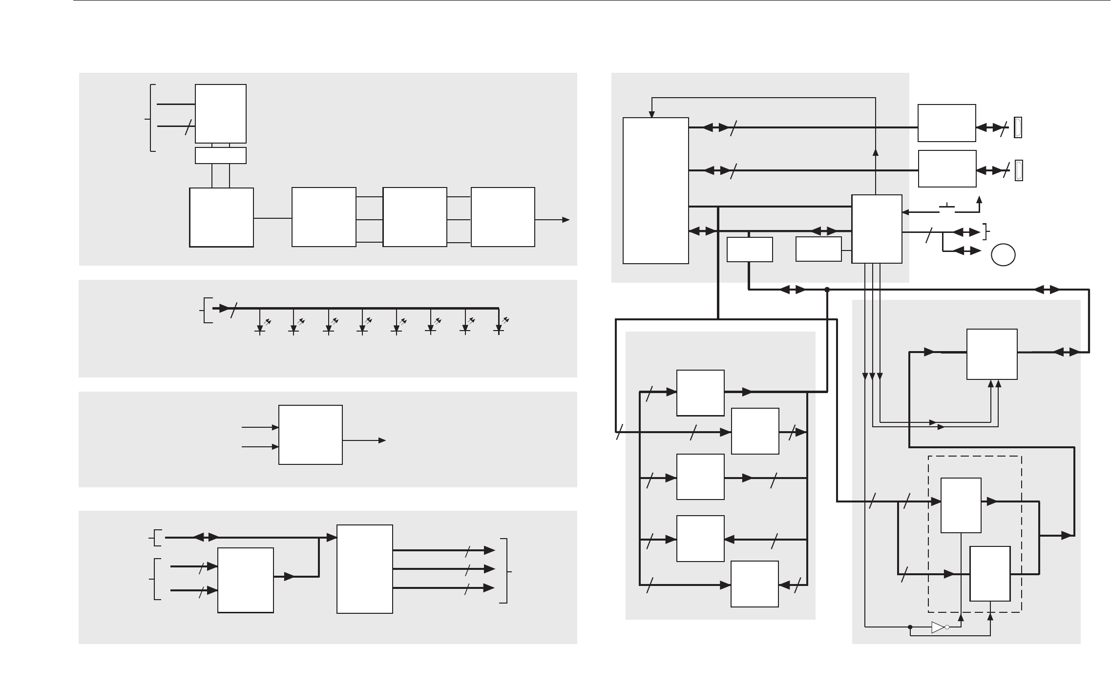
68P81095E02-D 4/16/99
2-25
EBTS System Manual - Vol 2 800/900/1500 MHz Base Radios
2
ETHERNET
SERIAL
INTERFACE
ISOLATION
TRANSFORMER TRANSCEIVER
HOST BUFFERED DATA BUS
HOST ADDRESS BUS
HOST BUFFERED DATA BUS
HOST ADDRESS BUS
HOST DATA BUS
DRAM ADDRESS
MULTIPLEXER
COLUMN/ROW
SELECT
DRAM
COLUMN
ADDRESS
DRAM
ROW
ADDRESS
16.5 MHZ CLK
SERIAL COMMUNICATIONS BUS
SERIAL COMMUNICATIONS BUS
ROW
SELECT
(RAS*)
COL
SELECT
(CAS*)
DRAM
ADDRESS
HOST
GLUE
ASIC
33 MHZ
TIMING
CIRCUITRY
BUFFERS
EPROM
512K X 8
8K X 8
EEPROM
CODEPLUG
32K X 8
SRAM
32K X 8
SRAM
A1-A11
A10-A22
A1-A19
A1-A19
A1-A15
HOST
ADDRESS
A1-A18
4
8
STATUS PORT
(9 PIN D CONNECTOR
ON BRC FRONT PANEL)
RS-232 PORT
(9 PIN D CONNECTOR
ON BACKPLANE)
EIA-232
BUS
RECEIVERS/
DRIVERS
4
8
EPROM
512K X 8
BUFFERS
SPI BUS
SPI BUS
TO/FROM
STATION MODULES
3
HOST ADDRESS BUS
NON-VOLATILE MEMORY
HOST
MICRO-
PROCESSOR
HOST MICROPROCESSOR / HOST ASIC
HOST
ADDRESS
1-23
EIA-232
BUS
RECEIVERS/
DRIVERS
DRAM MEMORY
BUFFERS
VARIOUS INPUTS
FROM BRC &
STATION CIRCUITRY
INPUT/OUTPUT PORTS CIRCUITRY
I/O PORT P0 IN
HOST DATA BUS
I/O PORT P0 OUT
I/O PORT P1 OUT
I/O PORT P2 OUT
VARIOUS
CONTROL
LINES TO BRC &
STATION
CIRCUITRY
FROM HOST
MICROPROCESSOR
I/O PORT P1 IN
BUFFERS
BUFFERS
16
16
16
16
16
REMOTE STATION
SHUTDOWN CIRCUITRY
SHUTDOWN
(TO POWER
SUPPLY)
28V
I/O PORT
P2 OUT
FRONT PANEL LEDS
LED CONTROL
LINES
(P/O I/O PORT
P0 OUT)
BASE
RADIO POWER
SUPPLY EXCITER PA CTL R1 R2 R3
8
ETHERNET INTERFACE
CD
RX
TX
CLSN
RCV
TRMT
FROM
HOST
MICROPROCESSOR
ADDR BUS
DATA BUS
COPROCESSOR
ADDR BUS COPROCESSOR
DATA BUS
10BASE2
COAX
ETHERNET
SERIAL
INTERFACE
HOST
INTERFACE
ETHERNET
COPROCESSOR
(82596DX)
A
EBTS286
010397SN
D0-D15
LANIIC
SHUTDOWN
CIRCUITRY
A1-A15
A1-A15
D0-D15
D0-D7
D0-D15
D0-D15
VCC RESET SWITCH
(FRONT PANEL)
DRAM
1M X 16
A2-A23
S
ingle
C
hannel Base Radio
C
ontroller
Figure:2-6
800/900 MHz Base Radio Controller Functional Block Diagram
(Sheet 1 of 2)

26
68P81095E02-D 4/16/99
800/900/1500 MHz Base Radios EBTS System Manual - Vol 2
TISIC INTERFACE CIRCUITRY
TISIC
16.8 MHZ
IN
2.1 MHZ
OUT
RX1 DATA
RX1 SERIAL
RESET
ADDRESS
DATA
16.8 MHZ TO ASIC
2.1 MHZ FROM DSP ASIC
RX2 DATA
RX2 SERIAL
RX3 DATA
RX3 SERIAL
STATION REFERENCE CIRCUITRY
16.8 MHZ TO ASIC
CONTROL VOLTAGE
ENABLE SWITCH
CONTROL VOLTAGE
5 MHZ REF
SPI BUS
5 MHz/1PPS
BNC CONNECTOR
ON BACKPLANE
2.1 MHZ REF TO EXCITER
MODULE VIA BACKPLANE
2.1 MHZ REF TO RECEIVER
MODULE #1, 2, 3 VIA BACKPLANE
16.8 MHZ
3
3
DIGITAL SIGNAL PROCESSOR (DSP) / DSP ASIC
DSP DATA BUS
RECEIVE SYNCHRONOUS
SERIAL INTERFACE BUS
(RXSSI)
SYNCHRONOUS SERIAL
INTERFACE (SSI)
FROM
HOST
MICRO-
PROCESSOR
HOST
DATA
BUS
HOST
ADDRESS
BUS
3
DIGITAL SIGNAL PROCESSOR
(DSP) / DSP ASIC
TRANSMIT
DIGITAL
SIGNAL
PROCESSOR
(TXDSP)
ADDRESS
DATA
HOST
PORT
SERIAL
COMMUNICATIONS
INTERFACE (SCI)
SYNCHRONOUS
SERIAL INTERFACE (SSI)
TRANSMIT SYNCHRONOUS
SERIAL INTERFACE (TXSSI)
FROM
HOST
MICRO-
PROCESSOR HOST
ADDRESS
BUS
HOST
DATA
BUS
CLOCK
OSCILLATOR
3
3
3
RECEIVE
DIGITAL
SIGNAL
PROCESSOR
(RXDSP)
HOST
PORT
ADDRESS
DATA
32K X 8
RAM
32K X 8
RAM
32K X 8
RAM
32K X 8
RAM
32K X 8
RAM
32K X 8
RAM
32K X 8
RAM
32K X 8
RAM
32K X 8
RAM
SERIAL BUS SERIAL BUS
DIFFERENTIAL DATA
FROM RECEIVER MODULE #1
VIA BACKPLANE
RX1 DATA
SERIAL BUS
TO/FROM
RECEIVER
MODULE #1
66
SERIAL BUS SERIAL BUS
DIFFERENTIAL DATA
FROM RECEIVER MODULE #2
VIA BACKPLANE
RX2 DATA
SERIAL BUS
TO/FROM
RECEIVER
MODULE #2
66
SERIAL BUS SERIAL BUS
DIFFERENTIAL DATA
FROM RECEIVER MODULE #3
VIA BACKPLANE
RX3 DATA
SERIAL BUS
TO/FROM
RECEIVER
MODULE #3
66
DIFFERENTIAL DATA
TO EXCITER MODULE
VIA BACKPLANE
4.8 MHz TRANLIN CLOCK
TO EXCITER MODULE
VIA BACKPLANE
A
3
SERIAL
COMMUNICATIONS
INTERFACE (SCI)
3
TXLIN
DATA
4.8 MHz TXLIN
CLOCK
PHASE
LOCKED
LOOP
IC
FIN
OSCIN
HIGH
STABILITY
VCXO
BUFFER/
SPLITTER
BUFFERS
DIFFERENTIAL-TO-TTL
CONVERTER/BUFFER
BUFFERS
DIFFERENTIAL-TO-TTL
CONVERTER/BUFFER
BUFFERS
DIFFERENTIAL-TO-TTL
CONVERTER/BUFFER
TTL-TO-DIFFERENTIAL
CONVERTER/BUFFER
TTL-TO-DIFFERENTIAL
CONVERTER/BUFFER
EBTS292
122094JNM
AGC
4TO RECEIVERS (1-3)
1PPS 5MHz/1PPS COMBINED SIGNAL
ENABLE
INPUT
Base Radio Controller
Figure:2-7
800/900 MHz Base Radio Controller Functional Block Diagram
(Sheet 2 of 2)

68P81095E02-D 4/16/99
2-27
EBTS System Manual - Vol 2 800/900/1500 MHz Base Radios
Base Radio Controller
Functional Block Diagram
Model TLN3425
(Includes Front Panel Board)
HOST
ADDRESS
A1-A23
SERIAL COMMUNICATIONS BUS (SCC3)
SERIAL COMMUNICATIONS BUS (SCC2)
HOST BUFFERED DATA BUS
HOST ADDRESS BUS
HOST BUFFERED DATA BUS
HOST ADDRESS BUS
HOST DATA BUS
DRAM ADDRESS
MULTIPLEXER
COLUMN/ROW
SELECT
DRAM
COLUMN
ADDRESS
DRAM
ROW
ADDRESS
ROW
SELECT
(RAS*)
COL
SELECT
(CAS*)
COL
SELECT
(CAS*)
ROW
SELECT
(RAS*)
DRAM
ADDRESS
DRAM
ADDRESS
HOST
ASIC
33 MHZ
TIMING
CIRCUITRY
BUFFERS
EPROM
256K X 8
8K X 8
EEPROM
CODEPLUG
8K X 8
SRAM
8K X 8
SRAM
A1-A11
A10-A22
A1-A18
A1-A18
A1-A15
4
8
EIA-232
BUS
RECEIVERS/
DRIVERS
6
9
EPROM
256K X 8
SPI BUS
SPI BUS
TO/FROM
STATION MODULES
3
HOST ADDRESS BUS
NON-VOLATILE MEMORY
HOST
MICRO-
PROCESSOR
HOST MICROPROCESSOR / HOST ASIC
DRAM
1M X 8
DRAM
1M X 8
HOST
ADDRESS
1-23
EIA-232
BUS
RECEIVERS/
DRIVERS
DYNAMIC RAM
VARIOUS INPUTS
FROM BRC &
STATION CIRCUITRY
INPUT/OUTPUT PORTS CIRCUITRY
I/O PORT P0 IN
HOST DATA BUS I/O PORT P0 OUT
I/O PORT P1 OUT
I/O PORT P2 OUT
I/O PORT P3 OUT
VARIOUS
CONTROL
LINES TO BRC &
STATION
CIRCUITRY
FROM HOST
MICROPROCESSOR
I/O PORT P1 IN
LATCHES
BUFFERS
16
16
16
16
16
16
REMOTE STATION
SHUTDOWN CIRCUITRY
SHUTDOWN
(TO POWER
SUPPLY)
28V
I/O PORT
P3 OUT
FRONT PANEL LEDS (Part of TRN7769)
LED CONTROL
LINES
(P/O I/O PORT
P0 OUT)
BASE
RADIO POWER
SUPPLY EXCITER PA BRC RX1 RX2 RX3
8
ETHERNET INTERFACE
CD
RX
TX
CLSN
RCV
TRMT
FROM
HOST
MICROPROCESSOR
ADDR BUS
DATA BUS
COPROCESSOR
ADDR BUS COPROCESSOR
DATA BUS
10BASE2
COAX
ETHERNET
SERIAL
INTERFACE
82596DX
ETHERNET
COPROCESSOR
ETHERNET
SERIAL
INTERFACE TRANSCEIVER
A
HOST
INTERFACE
ISOLATION
TRANSFORMER
SHUTDOWN
CIRCUITRY
BUFFERS
BUFFERS
16.5 MHZ CLK
DC/DC
CONVERTER
5 VDC
-9 VDC
23
16
20 MHZ
TIMING
CIRCUIT
20 MHz
XMT CLK
(10 MHZ)
A1-A13
A1-A13
STATUS
(9 PIN D CONNECTOR
ON BRC FRONT PANEL)
RS232
(9 PIN D CONNECTOR
ON BACKPLANE)
STATIC RAM
Figure:2-8
1500 MHz Base Radio Controller Functional Block Diagram
(Sheet 1 of 2)
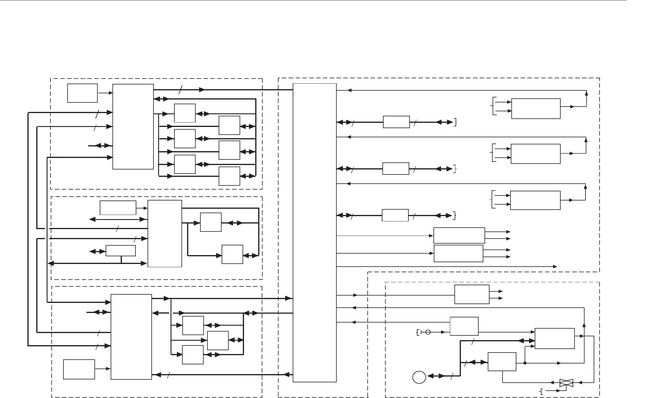
28
68P81095E02-D 4/16/99
800/900/1500 MHz Base Radios EBTS System Manual - Vol 2
Base Radio Controller
Functional Block Diagram
Model TLN3425
(Includes Front Panel Board)
HOST ADDRESS
BUS FROM HOST
MICROPROCESSOR
LATCH
ERROR
CORRECTION
DIGITAL
SIGNAL
PROCESSOR
DSP DATA BUS
32K X 8
RAM
32K X 8
RAM
32K X 8
RAM
TRANSMIT SYNCHRONOUS
SERIAL INTERFACE (TXSSI)
3
32K X 8
RAM
32K X 8
RAM 32K X 8
RAM
32K X 8
RAM 32K X 8
RAM
32K X 8
RAM
SCI
3
SSI
3
DSP ASIC INTERFACE CIRCUITRY
DSP
GLUE
ASIC
16.8 MHZ
IN
2.1 MHZ
OUT
RX1 DATA
RX1 SERIAL
16.8 MHZ TO ASIC
2.1 MHZ FROM DSP ASIC
RX2 DATA
RX2 SERIAL
RX3 DATA
RX3 SERIAL
STATION REFERENCE CIRCUITRY
PHASE
LOCKED
LOOP IC
16.8 MHZ TO ASIC
CONTROL VOLTAGE
ENABLE SWITCH
CONTROL VOLTAGE
FREQUENCY NET ENABLE
(I/O PORT P1 OUT)
5 MHZ FROM
EXTERNAL
REFERENCE
(FOR NETTING
PENDULUM)
5 MHZ REF
SPI BUS
BNC CONNECTOR
ON BACKPLANE
2.1 MHZ REF TO EXCITER
MODULE VIA BACKPLANE
2.1 MHZ REF TO RECEIVER
MODULE #1, 2, 3 VIA BACKPLANE
SPI BUS 16.8 MHZ
FIN
OSCIN
HIGH
STABILITY
VCO
3
3
3
DIGITAL SIGNAL PROCESSOR (DSP) / DSP ASIC
TRANSMIT
DIGITAL
SIGNAL
PROCESSOR
ADDRESS
DATA
SERIAL BUS SERIAL BUS
DIFFERENTIAL DATA
FROM RECEIVER MODULE #1
VIA BACKPLANE
RX1 DATA
SERIAL BUS
TO/FROM
RECEIVER
MODULE #1
66
BUFFERS
DIFFERENTIAL-TO-TTL
CONVERTER/BUFFER
SERIAL BUS SERIAL BUS
DIFFERENTIAL DATA
FROM RECEIVER MODULE #2
VIA BACKPLANE
RX2 DATA
SERIAL BUS
TO/FROM
RECEIVER
MODULE #2
66
BUFFERS
DIFFERENTIAL-TO-TTL
CONVERTER/BUFFER
SERIAL BUS SERIAL BUS
DIFFERENTIAL DATA
FROM RECEIVER MODULE #3
VIA BACKPLANE
RX3 DATA
SERIAL BUS
TO/FROM
RECEIVER
MODULE #3
66
BUFFERS
DIFFERENTIAL-TO-TTL
CONVERTER/BUFFER
DIFFERENTIAL DATA
TO EXCITER MODULE
VIA BACKPLANE
TTL-TO-DIFFERENTIAL
CONVERTER/BUFFER
DIFFERENTIAL DATA
TO EXCITER MODULE
VIA BACKPLANE
TTL-TO-DIFFERENTIAL
CONVERTER/BUFFER
A
BUFFER/
SPLITTER
1 PPS
STRIPPER
PAL
1 PPS
1 PPS
IN
40 MHZ
TIMING
CIRCUITRY
ADDRESS
DATA
DIGITAL SIGNAL PROCESSOR (DSP) / DSP ASIC
RECEIVE
DIGITAL
SIGNAL
PROCESSOR
ADDRESS
DATA
40 MHZ
TIMING
CIRCUITRY
RECEIVE SYNCHRONOUS
SERIAL INTERFACE BUS
(RXSSI)
3
DIGITAL SIGNAL PROCESSOR (DSP) / DSP ASIC
32K X 8
RAM
32K X 8
RAM
ADDRESS
DATA
HOST
PORT
LATCH ADDRESS
BUS
HOST DATA BUS
FROM HOST
MICROPROCESSOR
HOST DATA BUS
FROM HOST
MICROPROCESSOR
LATCH ADDRESS
BUS
SCI
SSI
3
3
HOST
PORT
LATCH ADDRESS BUS
10 MHZ TIMING
CIRCUITRY
HOST DATA BUS
FROM HOST
MICROPROCESSOR
SSI
3
SSI
3
AGC
TO RECEIVER
VIA BACKPLANE
AGC
TXLIN
DATA
TXLIN
CLOCK
Figure:2-9
1500 MHz Base Radio Controller Functional Block Diagram
(Sheet 2 of 2)
68P81095E02-D 12/4/2000
2--29
EBTS System Manual - Vol 2 800/900/1500 MHz Base Radios
Base Radio Controller
2
SPI
BUS
PHASE
DETECTION/
FILTERING
HIGH
STABILITY
VCXO
48 MHZ
16.8MHZ
QUAD Channel Base
Radio Controller
Functional Block Diagram
Figure:2-10
QUAD CHANNEL Base Radio Controller Functional Block Diagram
(Sheet 1 of 2)
POWER
SUPPLY EXCITER/
CONTROL PA REF RX1 RX2 RX3 RX4 TX1 TX2 TX3 TX4
P0 OUT
LED
CONTROL
LINES
HOST
LATCH
12
FRONT PANEL LEDS REMOTE STATION
3.3V
P0_OUT
SHUTDOWN
CIRCUITRY
SHUTDOWN
(TO POWER
SUPPLY)
SHUTDOWN CIRCUITRY
SYNTHESIZER
IC / CIRCUITRY
5MHZ_1PPS
BASE RADIO
INPUT
HIGH
STABILITY
VCXO
PHASE
DETECTION/
FILTERING/
CONTROL
STEARING
LINE
DISCONNECT/
CONNECT
CONTROL
G
A
T
I
N
G
SPI
BUS
16.8 MHZ
SYNTHESIZER
IC / CIRCUITRY
STEARING
LINE
STATION REFERENCE CIRCUITRY
TRANSMIT REFERENCE CIRCUITRY
5MHZ
1PPS
2--30
68P81095E02-D 12/4/2000
800/900/1500 MHz Base Radios EBTS System Manual - Vol 2
Base Radio Controller
QUAD Channel
Base Radio Controller
Functional Block Diagram
Figure:2-11
QUAD CHANNEL Base Radio Controller Functional Block Diagram
(Sheet 2 of 2)
HOST
MICRO-
ETHERNET
SERIAL
INTERFACE
TRANS-
CD
RCV RX
TRMT TX
CLSN
10BASE2
COAX
ETHERNET
SERIAL
INTERFACE
CEIVER
ISOLATION
TRANSFORMER
PROCESSOR
SCC1
8
SDRAM
4M x 16
SDRAM
4M x 16
SDRAM
4M x 16
SDRAM
4M x 16
GPLA0, A[8,9,17,18,20:29],RAS,CAS,WE
CS2
CS3
D[0:31]
D[0:15]
D[16:31]
D[0:15]
D[16:31]
BUFFER
BUFFER
BUFFER
BUFFER
BUFFER
BUFFER
D[0:31]
D[0:7]
A[10:31]
MA[21:0]
DSP_D[31:24]
A[0:7]
DSP_A[31:24]
MD[31:0]
EIA-232
BUS
RECEIVERS/
DRIVERS
2STATUS PORT
(9 PIN D CONNECTOR
ON BRC FRONT PANEL)
2
BUFFER
33SPI BUS
TO/FROM
STATION MODULES
FLASH
1M x 16
FLASH
1M x 16
FLASH
1M x 16
FLASH
1M x 16
CS0
CS1
MD[0:15]
MD[16:31]
MD[0:15]
MD[16:31]
16
16
16
16
16 16
16
16
MA[2:21]
MA[2:21]
EEPROM
32k x 8
MD[24:31]
MA[0:14]
CS4
P1_OUT
LATCH
P0_OUT
LATCH
MD[0:32]
MD[24:31]
P0_IN
BUFFER
MD[16,17,20-24,28-31]
STATUS BUS
FROM
STATION MODULES
P0_IN
8
CONTROL BUS
TO
STATION MODULES
P0_OUT/P1_OUT
32
8
TRANSMIT
DIGITAL
SIGNAL
PROCESSOR
(TX DSP)
SINGLE END
TO DIFFERENTIAL
TRANSMIT
CLOCK AND
FRAME SYNCH
CIRCUITRY
I/Q DATA
SERIAL DATA
TO EXCITER
DIFFERENTIAL
TO SINGLE END
RX1 SERIAL DATA
RECEIVE
DIGITAL
SIGNAL
PROCESSOR
(RX DSP 1)
RECEIVE
DIGITAL
SIGNAL
PROCESSOR
(RX DSP 2)
TISIC
A[0:5]
D[0, 8:23]
PARALLEL
TO SERIAL
CIRCUITRY
D[16:23]
D[16:23]
D[0, 23]
SPI BUS TO
RECEIVER 1 & 2
SPI BUS TO
RECEIVER 3 & 4
2.4 MHz
1 PPS TIMING, CONTROL/ SLOT TIMING/RESET
NETWORKED
SCI
16.8MHZ
48 MHZ
SPI
BUS
SPI
BUS
EXCITER
SPI
CONTROL
DSP SPI
SPI BUS
TO EXCITER
DIGITAL SIGNAL PROCESSING
CIRCUITRY
DIGITAL SIGNAL PROCESSING
CIRCUITRY
DIFFERENTIAL
TO SINGLE END
DIFFERENTIAL
TO SINGLE END
DIFFERENTIAL
TO SINGLE END
50 MHZ
CLOCK
FRONT PANEL
RESET
DRAM MEMORY
ETHERNET INTERFACE
NON-VOLATILE MEMORY EXPANDED STATUS INPUT
AND OUTPUT CONTROL CIRCUITRY
EXTENDED HOST
BUS BUFFERS
40
TO EXCITER
5MHZ
1PPS
RX2 SERIAL DATA
RX3 SERIAL DATA
RX4 SERIAL DATA
HOST ADDRESS BUS
HOST DATA BUS
HOST BUFFERED DATA BUS
HOST BUFFERED ADDRESS BUS
HOST-DSP BUFFERED DATA BUS
HOST-DSP BUFFERED ADDRESS BUS
SERIAL MANAGEMENT CONTROLLER (SMC2)
SERIAL PERIPHERAL INTERFACE

68P81095E02-D 11/9/2000
3-1
EBTS System Manual - Vol 2 800/900/1500 MHz Base Radios
3 Exciter
Overview
This section provides technical information for the Exciter (EX). Table 3-1
describes covered topics.
FRU Number to Kit Number Cross Reference
Exciter Field Replaceable Units (FRUs) are available for the iDEN EBTS. The FRU
contains the Exciter kit and required packaging. Table 3-2 provides a cross
reference between Exciter FRU numbers and kit numbers.
Table 3-1
Chapter Topics
Chapter Page Description
800 MHz Exciter Ð TLN3337;
900 MHz Exciter Ð CLN1357;
1500 MHz Exciter Ð TLN3428
3-2 Describes the functions and characteristics of the Exciter
module for the single channel Base Radio (BR).
QUAD Channel 800 MHz Exciter 3-7 Describes the functions and characteristics of the Exciter
module for the QUAD channel Base Radio (BR).
Exciter 800 MHz Functional 3-11 Functional Block Diagram for the Single Channel Base Radio
Exciter
800 MHz QUAD ChannelFunctional Block Diagram 3-13 Functional Block Diagram for the QUAD Channel Base
Radio Exciter
Table 3-2
FRU Number to Kit Number Cross Referece
Description FRU Number Kit Number
Single Channel Exciter (800 MHz) TLN3337 CLF1490
Single Channel Exciter (900 MHz) CLN1357 CLF1500
Single Channel Exciter (1500 MHz) TLN3428 CTX1120
QUAD Channel Exciter/Base Radio Controller
(800 MHz)
CLN1497 CLF1560
3-2
68P81095E02-D 11/9/2000
800/900/1500 MHz Base Radios EBTS System Manual - Vol 2
800 MHz Exciter – TLN3337; 900 MHz Exciter – CLN1357; 1500 MHz Exciter – TLN3428
800 MHz Exciter – TLN3337;
900 MHz Exciter – CLN1357;
1500 MHz Exciter – TLN3428
Exciter Overview
The Exciter, together with the Power AmpliÞer (PA), provides the transmitter
functions for the Base Radio. The Exciter module consists of a printed circuit
board, a slide-in housing, and associated hardware.
The Exciter connects to the Base Radio backplane through a 96-pin DIN connector
and two blindmate RF connectors. Two
Torx screws on the front of the Exciter
hold it in the chassis.
The Exciter has no controls or indicators. The manualÕs Base Radio section
supplies transmitter circuitry speciÞcations, including Exciter and PA
speciÞcations.
Figures 3-1 and 3-2 show the Exciter with the cover removed.
Figure:3-1
800/900 MHz Exciter (with cover removed)
68P81095E02-D 11/9/2000
3-3
EBTS System Manual - Vol 2 800/900/1500 MHz Base Radios
800 MHz Exciter – TLN3337; 900 MHz Exciter – CLN1357; 1500 MHz Exciter – TLN3428
Theory of Operation
Table 3-3 lists and describes basic Exciter circuitry. Figures 3-4 and 3-5 show the
functional block diagram of the Single Carrier Exciter. Figures 3-6 show the
functional block diagram of the QUAD Carrier Exciter.
Address Decoder Circuitry
The address decoder circuitry enables the BRC to use the address bus to control
Exciter circuitry. The BRC can select a speciÞc device on the Exciter via the SPI
bus for control or data communication purposes.
If board select circuitry decodes address lines A2 through A5 as the Exciter
address, the BRC enables the chip select circuitry. The chip select circuitry then
decodes address lines A0 and A1 to generate the chip select signals for the
EEPROM, A/D converter, Tranlin IC, and PLL IC. Once selected, the BRC uses
the SPI bus to send and receive data to and from the device.
Memory Circuitry
The memory circuitry consists of an EEPROM located on the Exciter. The BRC
performs all memory read and write operations via the SPI bus. Information
1.5GHZ-B859
Figure:3-2
1500 MHz Exciter, version TLN3428 (with top removed)

3-4
68P81095E02-D 11/9/2000
800/900/1500 MHz Base Radios EBTS System Manual - Vol 2
800 MHz Exciter – TLN3337; 900 MHz Exciter – CLN1357; 1500 MHz Exciter – TLN3428
stored in this memory device includes the kit number, revision number, module
speciÞc scaling and correction factors, and free form information (scratch pad).
A/D Converter Circuitry
Analog signals from various areas throughout the Exciter board are fed to the
A/D converter. Upon the BRCÕs request, these analog signals are converted to a
digital signal and are output to the BRC via the SPI lines. The BRC periodically
monitors and controls all signals.
Table 3-3
Exciter Circuitry
Circuit Description
Tranlin IC Performs the following functions:
¥ up-converts the baseband data to the Þrst IF
¥ down-converts the IF feedback signal to baseband
¥ uses a baseband Cartesian feedback loop system, which is
necessary to obtain linearity from the transmitter and
avoid splattering power into adjacent channels
¥ performs training functions for proper linearization of the
transmitter
Exciter IC Interfaces with Tranlin IC to perform:
¥ up-conversion from the Þrst IF to the transmit operating
frequency
¥ down-conversion to the IF of PA output feedback signal
for input to the Tranlin IC
Address Decode, Memory, &
A/D Converter
Serves as the main interface between the synthesizer, Tranlin
IC, A/D, and EEPROM on the Exciter and the BRC via the
SPI bus
Frequency Synthesizer
Circuitry
Consists of a phase-locked loop and VCO. Provides a LO
signal to the Exciter IC for the second up-conversion and for
the Þrst down-conversion of the feedback signal from the PA
970 MHz VCO (800 MHz BR)
1025 MHz VCO (900 MHz BR)
760 MHz VCO (1500 MHz BR)
Provides a LO signal to the Exciter IC for the second
up-conversion to the transmit frequency
237 MHz VCO (800 MHz BR)
236 MHz VCO (1500 MHz BR)
Provides a LO signal to Tranlin IC for the Þrst up-conversion
and for the second down-conversion of the feedback signal.
The synthesizer and divide by 2 circuitry within the Tranlin
IC set the Þrst IF to 118.5 MHz
180.6 MHz VCO (900 MHz BR) Provides a LO signal to Tranlin IC for the Þrst up-conversion
and for the second down-conversion of the feedback signal.
The synthesizer and divide by 2 circuitry within the Tranlin
IC set the Þrst IF to 90.3 MHz
Regulator Circuitry Provides a regulated voltage to various ICs and RF devices
located on the Exciter
Linear RF ampliÞer Stages AmpliÞes the RF signal from the Exciter IC to an appropriate
level for input to the PA
Automatic Gain Control (AGC) provides automatic gain control of the transmitter (Exciter and
Power AmpliÞer modules) to maintain a level forward gain of
the RF ampliÞer stages.

68P81095E02-D 11/9/2000
3-5
EBTS System Manual - Vol 2 800/900/1500 MHz Base Radios
800 MHz Exciter – TLN3337; 900 MHz Exciter – CLN1357; 1500 MHz Exciter – TLN3428
The BRC monitors the regulated voltages, the external wattmeter (optional), the
PLL circuit, and other internal signals.
Tranlin IC Circuitry
The Tranlin IC is a main interface between the Exciter and BRC. The Digital Signal
Processors (DSP) of the BRC send Digitized signals (baseband data) to the Exciter
via the DSP data bus. The DSP clock signal from the Receiver clocks these data
signals.
The differential data clock signal also serves as a 4.8 MHz reference signal to the
internal synthesizer circuit of the Tranlin IC. The Tranlin compares the reference
signal with the output of the 237 MHz or 180.6 MHz (900 MHz BR) or 236 MHz
(1500 MHz BR) Voltage Controlled Oscillator (VCO). If the VCO output is out of
phase or differs in frequency, correction pulses arrive at the Oscillator and adjust
the VCO output.
The Tranlin IC up-converts the baseband data received from the BRC to the Þrst IF
of 118.5 MHz (90.3 MHz for 900 MHz BR). It also down-converts an IF feedback
signal from the Exciter IC to baseband data for summing.
The Serial Peripheral Interface (SPI) bus is used to communicate with the Tranlin
IC. The SPI bus serves as a general purpose bi-directional serial link between the
BRC and other modules of the Base Radio, including the Exciter. The SPI bus is
used to send control and operational data signals to and from the various circuits
of the Exciter.
Exciter IC Circuitry
The Exciter IC interfaces directly with the Tranlin IC to perform up-conversion
from the Þrst IF to the programmed transmit operating frequency. The Þrst IF
signal is passed through a band-pass Þlter before it reaches the Exciter IC.
The Exciter IC also down-converts the RF feedback signal from the PA to its IF
signal. The IF signal is then input to the Tranlin IC for conversion to baseband
data, which computes the Cartesian feedback.
Synthesizer Circuitry
The synthesizer circuitry consists of the Phase-Locked Loop (PLL) IC and
associated circuitry. The output of this circuit is combined with the 970 MHz
VCO (1025 MHz for 900 MHz BR, 700 MHz for 1500 MHz BR) to supply a Local
Oscillator (LO) signal to the Exciter IC for the second up-conversion of the
programmed transmit frequency. This signal is also used for the Þrst
down-conversion of the feedback signal from the PA.
An internal phase detector generates a logic pulse in proportion to the difference
in phase or frequency between the reference frequency and loop pulse signal.
If the reference frequency is faster than the VCO feedback frequency, the PLL IC
outputs an up signal. If the reference frequency is slower than the VCO feedback
frequency, the PLL IC outputs a down signal. These pulses are used as correction
signals and are fed to a charge pump circuit.

3-6
68P81095E02-D 11/9/2000
800/900/1500 MHz Base Radios EBTS System Manual - Vol 2
800 MHz Exciter – TLN3337; 900 MHz Exciter – CLN1357; 1500 MHz Exciter – TLN3428
The charge pump circuit consists of Þve transistors and its associated biasing
components. This circuit generates the correction signal and causes it to move up
or down in response to the phase detector output pulses. The correction signal
passes through the low-pass loop Þlter to the 970 MHz Voltage Controlled
Oscillator (VCO) circuit (1025 MHz VCO for 900 MHz BR).
970/1025 MHz Voltage Controlled Oscillator (VCO)
The 970 MHz VCO (1025 MHz for 900 MHz BR, 700 MHz for 1500 MHz BR)
generates the second injection frequency for the Exciter IC.
The VCO requires a very low-noise DC supply voltage of +10 Vdc for proper
operation. A Super Filter, which contains an ultra low-pass Þlter, drives the
oscillator. The Super Filter obtains the required low-noise output voltage for the
oscillator.
The output of the oscillator is tapped and sent to the VCO Feedback Filter. This
feedback signal is supplied to the Synthesizer circuitry for the generation of
correction pulses.
The untapped output of the 970 (or 1025) MHz VCO is sent to the second LO
injection circuitry.
236/237/180.6 MHz Voltage Controlled Oscillator (VCO)
The 237 MHz VCO (180.6 MHz for 900 MHz BR, 236 MHz for 1500 MHz BR)
provides a LO signal to Tranlin IC for the Þrst up-conversion and for the second
down-conversion of the feedback signal. The synthesizer and divide by 2
circuitry within the Tranlin IC set the Þrst IF to 118.5 MHz (90.3 MHz for 900 MHz
BR).
Regulator Circuity
This circuit generates three regulated voltages of +5 Vdc, +10 Vdc, and +11.8 Vdc.
All voltages are obtained from the +14.2 Vdc backplane voltage. These voltages
provide power to various ICs and RF devices of the Exciter.
Linear RF Amplifier Stages
This circuitry is used to amplify the RF signal from the Exciter IC to an
appropriate level for input to the PA.
Automatic Gain Control (AGC) (1500 MHz only)
The Automatic Gain Control (AGC) circuit controls the output gain of the
transmitter (Exciter and Power AmpliÞer modules) so that constant forward gain
of the RF ampliÞer stages is maintained. This is accomplished through the
comparison of feedback signals from the Power AmpliÞer and the Þrst ampliÞer
stage of the Exciter.
The output of the differential ampliÞers is used to adjust the Attenuator and
Image Filter.
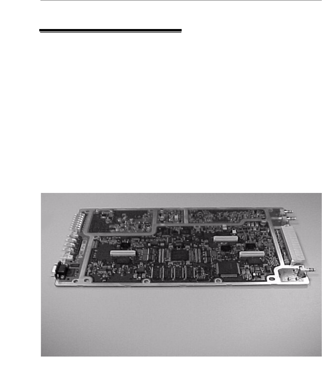
68P81095E02-D 11/9/2000
3-7
EBTS System Manual - Vol 2 800/900/1500 MHz Base Radios
QUAD Channel 800 MHz Exciter
QUAD Channel 800 MHz Exciter
Exciter Overview
The Exciter and the Power AmpliÞer (PA) provide the transmitter functions of the
QUAD Channel Base Radio. The Exciter module consists of a printed circuit
board, a slide in housing, and associated hardware. The BRC shares the printed
circuit board and housing.
The Exciter connects to the Base Radio backplane through a 168-pin connector
and two blindmate RF connectors. Controller and exciter circuitry also
interconnect on the Exciter/Controller module. Two
Torx screws on the front of
the Exciter secure it to the chassis.
An LED identiÞes the ExciterÕs operational condition, as described in the
manualÕs Controller section. The Base Radio section of the manual provides
speciÞcations for transmitter circuitry. This information includes data on the
Exciter and PAs.
Figures 3-3 shows the Exciter with the cover removed.
Figure:3-3
800 MHz QUAD Channel Exciter (with cover removed)M

3-8
68P81095E02-D 11/9/2000
800/900/1500 MHz Base Radios EBTS System Manual - Vol 2
QUAD Channel 800 MHz Exciter
Theory of Operation
Table 3-4 describes the basic circuitry of the Exciter. Figures 3-4 and 3-5 show the
functional block diagram of the Single Carrier Exciter. Figures 3-6 show the
QUAD Carrier ExciterÕs functional block diagram.
Memory Circuitry
The memory circuitry is an EEPROM on the Controller portion of the Exciter/
Controller module. The Controller performs memory read and write operations
over the SPI bus. The memory device stores the following data...
❐
kit number
❐
revision number
❐
module speciÞc scaling and correction factors
❐
serial number
Table 3-4
Exciter Circuitry
Circuit Description
LNODCT IC ¥ Up-converts baseband data to the transmit frequency
¥ Down-converts the PA feedback signal to baseband
¥ Uses a baseband Cartesian feedback loop system, necessary
to obtain linearity from the transmitter and avoid
splattering power into adjacent channels
¥ Performs training functions for proper linearization of the
transmitter
Memory & A/D Converter Serves as the main interface between the synthesizer, Tranlin
IC, A/D, and EEPROM on the Exciter, and the BRC via the
SPI bus
Frequency Synthesizer
Circuitry
¥ Consists of a phase-locked loop and VCO
¥ Provides a LO signal to the LNODCT IC for the second
up-conversion and first down-conversion of the feedback
signal from the PA
970 MHz VCO (800 MHz BR) Provides a LO signal to the LNODCT IC, for up-conversion
to the transmit frequency
90.3 MHz VCO (800 MHz BR) Provides a LO signal to LNODCT IC, for the up-conversion
and for the down-conversion of the feedback signal.
¥ The LNODCT IC mixes the 970 MHz VCO and 90.3 MHz
VCO
¥ The mixed output becomes the LO signal for Transmit
signal up- and down-conversion
Regulator Circuitry Provides a regulated voltage to various ICs and RF devices
located on the Exciter
Linear RF ampliÞer Stages AmpliÞes the RF signal from the Exciter IC to an appropriate
level for input to the PA
Automatic Gain Control (AGC) ¥ Provides automatic gain control of the transmitter (Exciter
and Power AmpliÞer modules)
¥ Maintains a level forward gain of the RF ampliÞer stages

68P81095E02-D 11/9/2000
3-9
EBTS System Manual - Vol 2 800/900/1500 MHz Base Radios
QUAD Channel 800 MHz Exciter
❐
free form information (scratch pad)
A/D Converter Circuitry
Analog signals from various areas throughout the Exciter board enter the
A/D converter (A/DC). The A/DC converts these analog signals to digital form.
Upon request of the BRC, A/DC output signals enter the BRC via SPI lines. The
Controller periodically monitors all signals.
Some of the monitored signals include ampliÞer bias and synthesizer signals.
LNODCT IC Circuitry
The LNODCT IC is a main interface between the Exciter and BRC. The BRCÕs
Digital Signal Processor (DSP) sends digitized signals (baseband data) to the
Exciter over the DSP data bus.
The differential data clock signal serves as a 4.8 MHz reference signal to the
LNODCT ICÕs internal synthesizer. The LNODCT compares the reference signal
with the outputs of Voltage Controlled Oscillators (VCOs). The LNODCT might
sense that a VCOÕs output is out of phase or off-frequency. If so, then the
LNODCT sends correction pulses to the VCO. The pulses adjust VCO output,
thereby matching phase and frequency with the reference.
The LNODCT IC up-converts baseband data from the BRC to the transmit
frequency. The LNODCT IC also down-converts the Transmit signal from the
Power AmpliÞer to baseband data for summing.
The BRC uses the Serial Peripheral Interface (SPI) bus to communicate with the
LNODCT IC. The SPI bus serves as a general purpose, bi-directional, serial link
between the BRC and other Base Radio modules, including the Exciter. The SPI
carries control and operational data signals to and from Exciter circuits.
Synthesizer Circuitry
The synthesizer circuit consists of the Phase-Locked Loop (PLL) IC and associated
circuitry. This circuitÕs output combines with the 970 MHz VCO signal. The result
is a Local Oscillator (LO) signal for the LNODCT IC. The LNODCT uses this LO
signal to up-convert the programmed transmit frequency. The LNODCT also
uses the LO signal to down-convert the PA feedback signal.
An internal phase detector generates a logic pulse. This pulse is proportional to
the phase or frequency difference between the reference frequency and loop pulse
signal.
If the reference frequency is faster than the VCO feedback frequency, the PLL IC
outputs an up signal. If the reference frequency is slower than the VCO feedback
frequency, the PLL IC outputs a down signal. The synthesizer uses these pulses as
correction signals and feed them to a charge pump circuit.
The charge pump circuit consists of Þve transistors and associated biasing
components. This circuit generates the correction signal. The correction signal
moves up or down in response to phase detector output pulses. The correction

3-10
68P81095E02-D 11/9/2000
800/900/1500 MHz Base Radios EBTS System Manual - Vol 2
QUAD Channel 800 MHz Exciter
signal passes through the low-pass loop Þlter. The signal then enters the 970 MHz
Voltage Controlled Oscillator (VCO) circuit.
970 MHz Voltage Controlled Oscillator (VCO)
The 970 MHz VCO generates the second injection frequency for the LNODCT IC.
For proper operation, the VCO requires a very low-noise, DC supply voltage. An
ultra low-pass Þlter prepares the necessary low-noise voltage and drives the
oscillator.
The tapped oscillator output signal enters the VCO Feedback Filter. The
Synthesizer circuitry uses this feedback signal in the generation of correction
pulses.
The untapped output signal of the 970 MHz VCO enters the second LO
injection circuit.
90.3 MHz Voltage Controlled Oscillator (VCO)
The synthesizer within the LNODCT IC sets the 90.3 MHz signal. The 90.3 MHz
VCO provides a LO signal to the LNODCT IC. The LNODCT uses this signal in
up-converting and down-converting the feedback signal.
Regulator Circuitry
The voltage regulator generates three regulated voltages: +3 Vdc, +5 Vdc and
+11.7 Vdc. The regulator obtains input voltages from the +3.3 Vdc and +14.2 Vdc
backplane voltages. The regulated voltages power various ICs and RF devices in
the Exciter.
Linear RF Amplifier Stages
The Linear RF AmpliÞer boosts the RF signal from the LNODCT IC. The RF
AmpliÞer outputs an appropriate signal level to drive the PA.
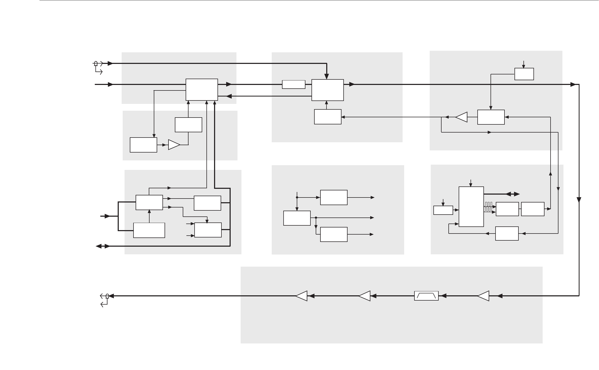
68P81095E02-D 4/1/2000
3-11
EBTS System Manual - Vol 2 800/900/1500 MHz Base Radios
Exciter
3
c
DIFFERENTIAL
DATA & CLOCK
FROM
BRC MODULE
ADDRESS BUS
FROM CONTROL
MODULE
SPI BUS
TO/FROM CONTROL
MODULE
ADDRESS DECODE, MEMORY, & A/D
CONVERTER CIRCUITRY
EXCITER IC CIRCUITRY 970 MHZ
(1025 MHZ)
VCO CIRCUITRY
SYNTHESIZER
CIRCUITRY
LINEAR RF AMPLIFIER
CIRCUITRY
2ND LO
INJECTION
CIRCUITRY
MEMORY
A/D
CONVERTER
CHIP SELECT
DECODE
CIRCUITRY
BOARD SELECT
DECODE
CIRCUITRY
VARIOUS
SIGNALS
TO MONITOR
SUPER
FILTER
+10 V
CONTROL VOLTAGE
(+2.5 TO +7.5 VDC)
OSCILLATOR
CHARGE
PUMP
2.1 MHZ
VCO FEEDBACK
CHIP
SELECT
SPI BUS (CLOCK & DATA)
FROM BACKPLANE
PHASE
LOCKED
LOOP
IC
RIN
FIN
CHIP
SELECT
237 MHZ
(180.6 MHZ)
VCO
CIRCUITRY
OSCILLATOR
BUFFER
AMP
TRANLIN IC CIRCUITRY
EXCITER IC
BPF
TISIC DATA & CLOCK
LOW-PASS
LOOP
FILTER
BUFFER
VCO
FEEDBACK
FILTER
1ST LO
INJECTION
CIRCUITRY
RF OUTPUT
TO PA MODULE
TRANLIN IC
IFOUT
IFIN
RF FEEDBACK
FROM PA MODULE
BUFFER
AMP
BPF
REGULATOR
CIRCUITRY
+11.8 V
REGULATOR
+14.2 V
FROM
BACKPLANE
+10 V
SOURCE
+11.8 V
SOURCE
ANALOG
+5 V SOURCE
+5 V
REGULATOR
+10 V
REGULATOR
(U3702)
EBTS283
101597JNM
NOTE: Where two frequencies are given, frequency without parentheses applies to 800 MHz BR only and frequency with parentheses applies to 900 MHz BR only.
Exciter
800 MHz Functional
Block Diagram
Figure:3-4
Exciter Functional Block Diagram

3-12
68P81095E02-D 4/1/2000
800/900/1500 MHz Base Radios EBTS System Manual - Vol 2
Exciter
Exciter
Functional Block Diagram
Model TLN3428
SPI BUS (CLOCK & DATA)
FROM BACKPLANE
DSP DATA AND CLOCK
FROM BRC MODULE
SPI BUS
TO/FROM
BRC MODULE
700 MHZ
VCO CIRCUITRY
SYNTHESIZER
CIRCUITRY
LINEAR RF AMPLIFIER
CIRCUITRY
AGC CIRCUITRY
SUPER
FILTER
(Q3300)
CONTROL VOLTAGE
(+2.5 TO +7.5 VDC)
OSCILLATOR
(Q3301)
CHARGE
PUMP
(Q3404, Q3405,
Q3406, Q3407,
Q3408)
2.1 MHZ
VCO FEEDBACK
PHASE
LOCKED
LOOP IC
(U3400)
RIN
FIN
AMP 4
(Q4002, Q4003) AMP 3
(Q4200, Q4201) AMP 2
(Q3902, Q3903)
236 MHZ VCO
CIRCUITRY
OSCILLATOR
(Q3201)
TRANLIN IC
CIRCUITRY
DSP DATA & CLOCK
SPI BUS (DATA & CLOCK)
LO-PASS
LOOP
FILTER
(U3401)
VCO
FEEDBACK
FILTER
(U3400)
RF OUTPUT
TO PA MODULE
TRANLIN IC
(U3600)
IFOUT
IFIN
RF FEEDBACK
FROM PA MODULE
OPEN LOOP
ALARM
TO A/D INTEGRATION/ATTN DRIVER
DIFF AMP
(U3801,
U3802)
RF FEEDBACK
FOR AGC
DIFF AMP
ATTENUATOR
IMAGE FILTER
(FL4000, FL4001
CR4000, CR4002)
1ST LO
INJECTION
CIRCUITRY
(L3201, C3206)
CONTROL VOLTAGE
(+2.5 TO +7.5 VDC)
REFERENCE
BUFFER
(Q3401)
AMP 1
(Q3900, Q3901)
EXCITER IC
CIRCUITRY
2ND LO
INJECTION
CIRCUITRY
(C4104, R3513)
RF FEEDBACK
FOR AGC DIFF AMP
EXCITER IC
(U3500)
BAND-PASS
FILTER
EXTERNAL
2.1 MHZ
REFERENCE
FREQUENCY
DOUBLER
(U4100, T4100,
CR4100)
+10 V
ADDRESS BUS
FROM BRC
SPI BUS
TO/FROM BRC
ADDRESS DECODE, MEMORY, & A/D
CONVERTER CIRCUITRY
MEMORY
(U3006)
A/D
CONVERTER
(U3100)
BOARD SELECT
DECODE
CIRCUITRY
(U3000)
VARIOUS
SIGNALS
TO MONITOR
CHIP SELECT
CHIP SELECT
DECODE
CIRCUITRY
(U3000)
REGULATOR
CIRCUITRY
+14.2 V
FROM
BACKPLANE
+10 V
SOURCE
+11.8 V
SOURCE
ANALOG
+5 V SOURCE
+11.8 V
REGULATOR
(U3701)
+10 V
REGULATOR
(U3702)
+5 V
REGULATOR
(U3703)
SUPER
FILTER
(Q3200)
+10 V
CHIP SELECT
CHIP SELECT
CHIP SELECT
RESET
RESET FROM
BRC MODULE
POWER
CONTROL
CHIP SELECT
Figure:3-5
Exciter Functional Block Diagram
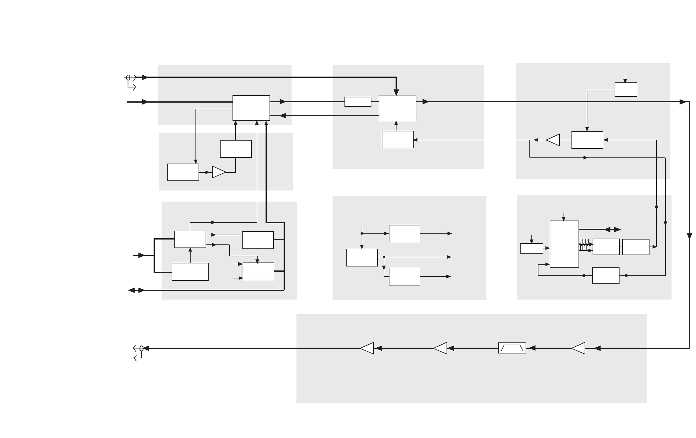
68P81095E02-D 11/10/2000
3-13
EBTS System Manual - Vol 2 800/900/1500 MHz Base Radios
Exciter
3
DIFFERENTIAL
DATA & CLOCK
FROM
BRC MODULE
ADDRESS BUS
FROM CONTROL
MODULE
SPI BUS
TO/FROM CONTROL
MODULE
ADDRESS DECODE, MEMORY, & A/D
CONVERTER CIRCUITRY
EXCITER IC CIRCUITRY 970 MHZ
(1025 MHZ)
VCO CIRCUITRY
SYNTHESIZER
CIRCUITRY
LINEAR RF AMPLIFIER
CIRCUITRY
2ND LO
INJECTION
CIRCUITRY
MEMORY
A/D
CONVERTER
CHIP SELECT
DECODE
CIRCUITRY
BOARD SELECT
DECODE
CIRCUITRY
VARIOUS
SIGNALS
TO MONITOR
SUPER
FILTER
+10 V
CONTROL VOLTAGE
(+2.5 TO +7.5 VDC)
OSCILLATOR
CHARGE
PUMP
2.1 MHZ
VCO FEEDBACK
CHIP
SELECT
SPI BUS (CLOCK & DATA)
FROM BACKPLANE
PHASE
LOCKED
LOOP
IC
RIN
FIN
CHIP
SELECT
237 MHZ
(180.6 MHZ)
VCO
CIRCUITRY
OSCILLATOR
BUFFER
AMP
TRANLIN IC CIRCUITRY
EXCITER IC
BPF
TISIC DATA & CLOCK
LOW-PASS
LOOP
FILTER
BUFFER
VCO
FEEDBACK
FILTER
1ST LO
INJECTION
CIRCUITRY
RF OUTPUT
TO PA MODULE
TRANLIN IC
IFOUT
IFIN
RF FEEDBACK
FROM PA MODULE
BUFFER
AMP
BPF
REGULATOR
CIRCUITRY
+11.8 V
REGULATOR
+14.2 V
FROM
BACKPLANE
+10 V
SOURCE
+11.8 V
SOURCE
ANALOG
+5 V SOURCE
+5 V
REGULATOR
+10 V
REGULATOR
(U3702)
EBTS283
101597JNM
NOTE: Where two frequencies are given, frequency without parentheses applies to 800 MHz BR only and frequency with parentheses applies to 900 MHz BR only.
T
HIS
P
ICTURE
MUST
BE
CHANGED
!
S
EE
MARK
-
UPS
Figure:3-6
Exciter Functional Block Diagram
E
xc
i
ter
800 MHz QUAD ChannelFunctional Block

68P81095E02-D 11/10/2000
3-14
EBTS System Manual - Vol 2 800/900/1500 MHz Base Radios
Exciter
This Page Intentionally
Left Blank

68P81099E10 D 11/9/2000
4-1
y
4
Power Amplifier
Overview
This section provides technical information for the Power AmpliÞer (PA). Table
4-1 describes covered topics.
FRU Number to Kit Number Cross Reference
Power Amplifer (PA) Field Replaceable Units (FRUs) are available for the iDEN
EBTS. The FRU contains the PAkit and required packaging. Table 4-2 provides a
cross reference between PA FRU numbers and kit numbers.
Table 4-1
Chapter Topics
Chapter Page Description
40W, 800 MHz Ð TLF2020 (TTF1580);
70W, 800 MHz Ð TLN3335 (CTF1040);
60W, 900 MHz Ð CLN1355 (CLF1300);
40W, 1500 MHz Ð TLN3426 (TLN3426);
800 MHz QUAD Ð CLF1400 (CLF1400)
4-2 Describes the functions and characteristics of the Base Radio
Power AmpliÞer (PA) module for the single and QUAD
Channel Base Radio (BR).
40W, 800 MHz Power AmpliÞer Ð TLF2020 (TTF1580) 4-15 Functional Block Diagram for the 40 Watt, 800 MHz, Single
Channel Base Radio Power AmpliÞer (PA)
70W, 800 MHz Power AmpliÞer Ð TLN3335 (CTF1040) 4-16 Functional Block Diagram for the 70 Watt, 800 MHz, Single
Channel Base Radio Power AmpliÞer (PA)
60W, 900 MHz Power AmpliÞer Ð CLN1355 (CLF1300) 4-17 Functional Block Diagram for the 60 Watt, 900 MHz, Single
Channel Base Radio Power AmpliÞer (PA)
40W, 1500 MHz Power AmpliÞer Ð TLN3426 4-18 Functional Block Diagram for the 40 Watt, 1500 MHz, Single
Channel Base Radio Power AmpliÞer (PA)
800 MHz QUAD Carrier Power AmpliÞer 4-19 Functional Block Diagram for the 800 MHz QUAD Channel
Base Radio Power AmpliÞer (PA)
Table 4-2
FRU Number to Kit Number Cross Referece
Description FRU Number Kit Number
40 W, 800 MHz Single Channel Base Radio PA TLF2020 CLF1772
70 W, 800 MHz Single Channel Base Radio PA TLN3335 CLF1771
60 W, 900 MHz Single Channel Base Radio PA CLN1355 CLN7125
40 W, 1500 MHz Single Channel Base Radio PA TLN3426 TTG1000
800 MHz QUAD Channel Base Radio PA CLF1499 CLF1400

4-2
68P81099E10 D 11/9/2000
y
40W, 800 MHz Ð TLF2020 (TTF1580); 70W, 800 MHz Ð TLN3335 (CTF1040); 60W, 900 MHz Ð CLN1355 (CLF1300); 40W, 1500 MHz
Ð TLN3426 (TLN3426); 800 MHz QUAD Ð CLF1400 (CLF1400)
40W, 800 MHz Ð TLF2020 (TTF1580);
70W, 800 MHz Ð TLN3335 (CTF1040);
60W, 900 MHz Ð CLN1355 (CLF1300);
40W, 1500 MHz Ð TLN3426 (TLN3426);
800 MHz QUAD Ð CLF1400 (CLF1400)
PA Overview
The Power Amplifier (PA), together with the Exciter, provides transmitter functions for
the QUAD Channel Base Radio. The PA accepts the low-level modulated RF signal from
the Exciter and amplifies the signal for transmission via the RF output connector.
The 800 MHz Base Radio can be equipped with either 40 Watt PA, TLF2020 (version
TTF1580) or 70 Watt PA, TLN3335 (version CTF1040). The 40W PA module consists of
five hybrid modules, four pc boards, and a module heatsink/housing assembly. The 70W
PA module consists of eight hybrid modules, four pc boards, and a module heatsink/
housing assembly.
The 900 MHz Base Radio is equipped with 60 Watt PA, CLN1355 (kit no. CLF1300A).
The PA module consists of four hybrid modules, two pc boards, and a module heatsink/
housing assembly.
The 1500 MHz Base Radio is equipped with 40 Watt PA, TLN3426. The PA module
consists of four hybrid modules, two pc boards, and the module heatsink/housing
assembly.
The 800MHz Quad Base Radio is equipped with the Quad PA, CLF1400. The PA module
consists of six hybrid modules, two pc boards, and the module heatsink/housing assembly.
The PA connects to the chassis backplane using a 96-pin DIN connector and three
blindmate RF connectors. Two Torx screws located on the front of the PA hold it in the
chassis.
Specifications of the transmitter circuitry, including the Exciter and PAs, are provided in
Base Radio Overview section. Figure 4-1 shows the 70W, 800 MHz PA. Figure 4-2 shows
the 60W, 900 MHz PA. Figure 4-3 shows the 40W, 1500 MHz PA.
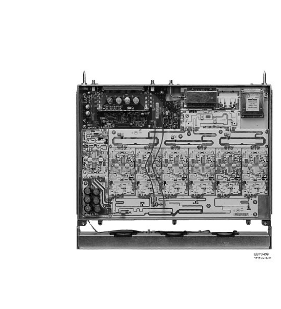
68P81099E10 D 11/9/2000
4-3
y
40W, 800 MHz Ð TLF2020 (TTF1580); 70W, 800 MHz Ð TLN3335 (CTF1040); 60W, 900 MHz Ð CLN1355 (CLF1300); 40W, 1500 MHz
Ð TLN3426 (TLN3426); 800 MHz QUAD Ð CLF1400 (CLF1400)
Figure:4-1 70W, 800 MHz PA Ð TLN3335 (with cover removed)
NOTE: 70W PA shown. 40W PA is similar.
4-4
68P81099E10 D 11/9/2000
y
40W, 800 MHz Ð TLF2020 (TTF1580); 70W, 800 MHz Ð TLN3335 (CTF1040); 60W, 900 MHz Ð CLN1355 (CLF1300); 40W, 1500 MHz
Ð TLN3426 (TLN3426); 800 MHz QUAD Ð CLF1400 (CLF1400)
Figure:4-2 60W, 900 MHz PA Ð CLN1355 (with cover removed)
68P81099E10 D 11/9/2000
4-5
y
40W, 800 MHz Ð TLF2020 (TTF1580); 70W, 800 MHz Ð TLN3335 (CTF1040); 60W, 900 MHz Ð CLN1355 (CLF1300); 40W, 1500 MHz
Ð TLN3426 (TLN3426); 800 MHz QUAD Ð CLF1400 (CLF1400)
1.5GHZ-Z858
Figure:4-3 40W, 1500 PA (with cover removed)
4-6
68P81099E10 D 11/9/2000
y
40W, 800 MHz Ð TLF2020 (TTF1580); 70W, 800 MHz Ð TLN3335 (CTF1040); 60W, 900 MHz Ð CLN1355 (CLF1300); 40W, 1500 MHz
Ð TLN3426 (TLN3426); 800 MHz QUAD Ð CLF1400 (CLF1400)
Figure:4-4 QUAD Channel PA (with cover removed)

68P81099E10 D 11/9/2000
4-7
y
Theory of Operation
Theory of Operation
Table 4-3 describes the basic functions of the PA circuitry. Figures 4-5, 4-6 and 4-9 show
the functional block diagrams of 40W, 800 MHz PA; 70W, 800 MHz PA and the 800MHz,
Quad PA, respectively. Figures 4-7 shows the functional block diagram of the 60W, 900
MHz PA. Figures 4-8 shows a functional block diagram of the 40W, 1500 MHz PA.
Table 4-3
Power Amplifier Circuitry
Circuit Description
DC/Metering Board ¥ Serves as the main interface between the PA and the backplane board
¥ Accepts RF input from the Exciter via a blindmate RF connector
¥ Routes the RF input via a 50 ½ stripline to the Linear Driver Module RF
amplifier
¥ Routes the RF feedback from the RF Combiner/Peripheral Module to the
Exciter via a blindmate RF connector
¥ Provides digital alarm and metering information of the PA to the BRC via
the SPI bus
¥ Routes DC power to the fans and PA
Linear Driver Module (LDM) ¥ Contains one Class AB stage which, in turn, drives a parallel Class AB stage
¥ Amplifies the low-level RF signal ~25 mW average power from the Exciter
via the DC/Metering Board (800MHz and 900MHz)
¥ Amplifies the low-level RF signal ~8 mW average power from the Exciter
via the DC/Metering Board (1500MHz)
¥ Provides an output of:
~10 W (800MHz) average power
~8 W (800MHz Quad) average power
~17 W (900MHz) average power
~16 W (1500MHz) average power
Interconnect Board
(800 MHz only)
¥ Provides RF interconnection from the LDM to the RF Splitter board
¥ Provides DC supply filtering
RF Splitter/DC board ¥ Interfaces with the DC/Metering Board to route DC power to the LFMs
¥ Contains splitter circuits that split the RF output signal of the LDM to the
three Linear Final Modules (40W, 800MHz)
¥ Contains splitter circuits that split the RF output signal of the LDM to the
six Linear Final Modules (70W, 800MHz and 800MHz Quad)
¥ Contains a Quadrature splitter circuit to split the RF output signal of the
LDM to the two Linear Final Modules (900 MHz and 1500 MHz)

4-8
68P81099E10 D 11/9/2000
y
Theory of Operation
DC/Metering Board(Non-Quad)
The DC/Metering Board provides the interface between the PA and the Base Radio
backplane. The preamplified/modulated RF signal is input directly from the Exciter via
the Base Radio backplane.
The RF input signal is applied to the input of the Linear Driver Module (LDM). The RF
feedback signal is fed back to the Exciter, where it is monitored for errors.
The primary function of the DC/Metering Boards is to monitor proper operation of the PA.
This information is forwarded to the Base Radio Controller (BRC) via the SPI bus. The
alarms diagnostic points monitored by the BRC on the PA include the following:
¥
Forward power
Linear Final Module
(LFM)
¥ Each module contains two Class AB amplifiers in parallel. Each module
amplifies one of three RF signals (~ 8 W average power) from the LDM
(via the Splitter/DC board). Three LFMs provide a sum RF output of
approximately 48 W average power. (40W, 800MHz)
¥ Each module contains two Class AB amplifiers in parallel. Each module
amplifies one of six RF signals (~ 8 W average power) from the LDM (via
the Splitter/DC board). Six LFMs provide a sum RF output of
approximately 97 W average power. (70W, 800MHz)
¥ Each module contains two Class AB amplifiers in parallel. Each module
amplifies one of six RF signals from the LDM (via the Splitter/DC board).
Six LFMs sum to provide the final RF power. (800MHz Quad)
¥ Each module contains two Class AB amplifiers in parallel. Each module
amplifies one of two RF signals (~ 17 W average power) from the LDM
(via the Splitter/DC board). Two LFMs provide a sum RF output of
approximately 75 W average power. (900MHz)
¥ Each module contains two Class AB amplifiers in parallel. Each module
amplifies one of two RF signals (~ 16 W average power) from the LDM
(via the Splitter/DC board). Two LFMs provide a sum RF output of
approximately 28 W average power. (1500MHz)
RF Interconnect Board
(40W, 800 MHz PA only)
¥ Contains three transmission lines that interconnect the LFMs to the RF
Combiner/Peripheral Module
Combiner Board
(70W, 800 MHz PA and
800MHz Quad only)
¥ Contains three separate Quadrature combiner circuits that respectively
combine the six RF outputs from the LFMs into three signals. These three
signals, in turn, are applied to the RF Combiner/Peripheral Module.
RF Combiner/Peripheral
Module
¥ Contains a combiner circuit that combines the three RF signals from the RF
Interconnect Board (40W PA) or the Combiner Board (70W PA and Quad
PA). It routes the combined RF signal through a circulator and a Low Pass
Filter. The final output signal is routed to the blindmate RF connector (800
MHz)
¥ Contains a Quadrature combiner circuit to combine the RF signal from the
two LFMs. It routes the combined RF signal through a circulator and a Low
Pass Filter. The output signal is routed to the blindmate RF connector (900
MHz and 1500 MHz)
¥ Contains an RF coupler that provides an RF feedback signal to the Exciter
via a blindmate RF connector. Also contains a forward and reverse power
detector for alarm and power monitoring purposes
Fan Assembly ¥ Consists of three fans used to keep the PA within predetermined operating
temperatures
Table 4-3
Power Amplifier Circuitry (Continued)
Circuit Description

68P81099E10 D 11/9/2000
4-9
y
Theory of Operation
¥
Reflected power
¥
PA temperature sense
DC/Metering Board (Quad only)
The DC/Metering Board in the Quad Radio serves the same function as does other radios.
However, its circuitry is modified to be compatible with the Quad Station. As such, the
logic circuitry is 3.3V.
In addition to the functions listed in the non-Quad version, the following metering points
are ported to the SPI bus:
¥
A and B Currents
¥
Fan Sensor
Linear Driver Module
800 MHz
The Linear Driver Module (LDM) amplifies the low-level RF signal from the Exciter.
The LDM consists of a two-stage cascaded amplifier.
The RF input signal applied to the LDM has an average power level of approximately 25
mW. The LDM amplifies this signal to an average output level of approximately 10 Watts.
(8W in Quad) The LDM output is fed to the RF Splitter/DC Distribution Board via an
Interconnect Board.
900 MHz
The Linear Driver Module (LDM) amplifies the low-level RF signal from the Exciter.
The LDM consists of a three-stage cascaded amplifier. This output is fed directly to the
RF Splitter/DC Distribution Board.
The RF input signal applied to the LDM has an average power level of approximately 25
mW. The LDM amplifies this signal to an average output level of approximately 17 Watts.
1500 MHz
The Linear Driver Module (LDM) takes the low level RF signal and amplifies it. The
LDM consists of a four stage cascaded amplifier. The RF input signal has an average
power level of 8 mW. The LDM amplifies the input signal to an average output level of
approximately 16 Watts. This output is fed directly to the RF Splitter/DC Distribution
Board.
The current drain of the Power Amplifiers is monitored by the A/D converter on the DC/
Metering board. A voltage signal representative of the LDM current drain is sent to the
BRC. A Power Amplifier alarm is generated if the signal is outside of either the upper or
lower limits.

4-10
68P81099E10 D 11/9/2000
y
Theory of Operation
Interconnect Board (800 MHz and 800MHz Quad only)
The output of the LDM is applied to the Interconnect Board, which provides an RF
connection to the RF Splitter/DC Distribution Board. As a separate function, area on the
Interconnect Board serves as a convenient mounting location for electrolytic capacitors
used for filtering the +28 VDC supply.
RF Splitter/DC Distribution Board
800 MHz
The RF Splitter portion of this board accepts the amplified signal from the LDM (via the
Interconnect Board). The primary function of this circuit is to split the RF signal into
drive signals for the LFMs.
In the 40W PA, this circuit splits the drive signal into three separate paths to be applied to
the three LFMs, where the signals will be amplified further. In the 70W PA and Quad PA,
this circuit splits the drive signal into six separate paths to be applied to the six LFMs,
where the signals will be amplified further.
The DC Distribution portion of this board interfaces directly with the DC/Metering Board
to route DC power to the LFMs.
900 MHz and 1500 MHz
The RF Splitter portion of this board accepts the amplified signal from the LDM. The
primary function of this circuit is to split the RF signal into two separate paths. These two
outputs are fed directly to two separate Linear Final modules where the RF signals will be
amplified further.
The DC Distribution portion of this board interfaces directly with the DC/Metering Board
to route DC power to the LFMs.
Linear Final Modules
800 MHz
The RF Splitter output signals are applied directly into the LFMs for final amplification.
Each LFM contains parallel PAs that amplify the RF signals.
In the 40W PA, the parallel LFMs amplify the input signals to a sum output level of
approximately 48 Watts average power. The amplified signal is then sent directly to the
RF Interconnect Board. In the 70W PA, the parallel LFMs amplify the input signals to a
sum output level of approximately 97 Watts average power. In the Quad PA, the function
is similar to the 70W PA. The amplified signal is then sent directly to the Combiner Board.
900 MHz
The RF signals from the outputs of the RF Splitter are applied directly into the Linear
Final Module (LFM) for final amplification. Each LFM contains dual PAs that amplify
the RF signals to a combined output level of approximately 75 Watts average power. The
amplified signal is then sent directly to the RF Combiner circuit for final distribution.

68P81099E10 D 11/9/2000
4-11
y
Theory of Operation
1500 MHz
The two RF signals from the outputs of the RF Splitter are input directly into the Linear
Final Module (LFM) for final amplification. Each LFM contains dual power amplifiers
that amplify the RF signals to an output equal to approximately 28 Watts average power.
The amplified signal is then sent directly to the RF Combiner circuit for final distribution.
The current drain of the Power Amplifiers is monitored by the A/D converter on the DC/
Metering board. A voltage signal representative of the LFM current drain is sent to the
BRC. A Power Amplifier alarm is generated if the signal is outside of either the upper or
lower limits.
RF Interconnect Board (40W, 800 MHz PA Only)
The RF Interconnect Board consists of transmission line paths which route the three
output signals from the LFMs to the three inputs of the RF Combiner/Peripheral Module.
Combiner Board (70W, 800 MHz PA and 800MHz Quad
PA Only)
The Combiner Board combines pairs of signals into single signals, thereby combining the
six signals from the LDMs into three signals. The resulting three signals are applied to the
RF Combiner/Peripheral Module.
RF Combiner/Peripheral Module
800 MHz and 800MHz Quad
This module consists of two portions: an RF combiner and a peripheral module. The RF
Combiner portion of the module combines the three RF signals from the RF Interconnect
Board (40W PA) or the Combiner Board (70W PA) into a single signal using a Wilkinson
coupler arrangement.
Following the combiner circuit, the single combined RF signal is then passed through a
directional coupler which derives a signal sample of the LFM RF power output. Via the
coupler, a sample of the RF output signal is fed to the Exciter as a feedback signal.
Following the coupler, the power output signal is passed through a circulator, which
protects the PA in the event of high reflected power.
The peripheral portion of the module provides a power monitor circuit that monitors the
forward and reflected power of the output signal. This circuit furnishes the A/D converter
on the DC/Metering Board with input signals representative of the forward and reflected
power levels.
For forward power, a signal representative of the measured value is sent to the BRC via
the SPI bus. The BRC determines if this level is within tolerance of the programmed
forward power level. If the level is not within parameters, the BRC will issue a warning to
the site controller which, in turn, will shut down the Exciter if required.
Reflected power is monitored in the same manner. The BRC uses the reflected power to
calculate the voltage standing wave ratio (VSWR). If the VSWR is determined to be
excessive, the forward power is rolled back. . If it is extremely excessive, the BRC issues
a shut-down command to the Exciter.

4-12
68P81099E10 D 11/9/2000
y
Theory of Operation
A thermistor is located on the RF Combiner/Peripheral module to monitor the operating
temperature of the PA. The thermistor signal indicating excessive temperature is applied
to the A/D converter and then sent to the BRC. The BRC rolls back forward power if the
monitored temperature is excessive.
900 MHz
The combined LFM output is applied to this module. The RF signal is first passed through
a directional coupler which derives a signal sample of the LFM RF power output. Via the
coupler, a sample of the RF output signal is fed to the Exciter as a feedback signal, thereby
allowing the Exciter to accordingly adjust signal drive. Following the coupler, the power
output signal is passed through a circulator, which protects the PA in the event of high
reflected power.
A power monitor circuit monitors the forward and reflected power of the output signal.
This circuit furnishes the A/D converter on the DC/Metering Board with input signals
representative of the forward and reflected power levels.
For forward power, a signal representative of the measured value is sent to the BRC via
the SPI bus. The BRC determines if this level is within tolerance of the programmed
forward power level. If the level is not within parameters, the BRC will issue a warning to
the site controller which, in turn, will shut down the Exciter if required.
Reflected power is monitored in the same manner. The BRC uses the reflected power to
calculate the voltage standing wave ratio (VSWR). If the VSWR is determined to be
excessive, the forward power is rolled back. If it is extremely excessive, the BRC issues a
shut-down command to the Exciter.
A thermistor is located on the RF Combiner/Peripheral module to monitor the operating
temperature of the PA. A voltage representative of the monitored temperature is sent from
the A/D converter to the BRC. The BRC rolls back forward power if the monitored
temperature is excessive.
1500 MHz
Both LFM outputs are input into this module where they are combined for a single output
signal. The RF signal is first coupled to the Exciter module so that it can be monitored.
The RF output signal is then passed through a circulator that acts as a protection device for
the PA in the event of reflected power.
A power monitor circuit monitors the forward and reflected power of the output signal.
This circuit provides the A/D converter on the DC/Metering board with an input signal
representative of the forward or reflected power levels.
For forward power, a signal representative of the measured value is sent to the BRC
module via the SPI bus. The BRC determines if this level is within tolerance of the
programmed forward power level. The programmed forward power is set through the use
of MMI commands. If the level is not within certain parameters, the BRC will issue a
warning to the site controller and may shut-down the Exciter module.
Reflected power is monitored in the same manner except that the BRC determines an
acceptable reflected power level. The BRC calculates the reflected power through an
algorithm stored in memory. If the reflected power is determined to be excessive, the
forward power is rolled back. If the reflected power level is extremely excessive, the BRC
will issues a shut-down command to the Exciter module.

68P81099E10 D 11/9/2000
4-13
y
Theory of Operation
A thermistor is located on the RF Combiner/Peripheral module to monitor the operating
temperature of the Power Amplifier. A voltage representative of the monitored
temperature is sent from the A/D converter to the BRC. The BRC issues a cut-back
command to the Exciter module if the monitored temperature is greater than 121û F (85û
C).
Fan Module
The PA contains a fan assembly to maintain normal operating temperature through the use
of a cool air intake. The fan assembly consists of three individual fans in which airflow is
directed across the PA heatsink.
The current draw of the fans is monitored by the DC/Metering Board. A voltage
representative of the current draw is monitored by the BRC. The BRC flags the iSC if an
alarm is triggered. The PA LED on the front panel of the BRC also lights, however the PA
does not shut down.

4-14
68P81099E10 D 11/9/2000
y
This Page Intentionally
Left Blank
68P81095E02-D 4/1/2000
4-15
EBTS System Manual - Vol 2 800/900/1500 MHz Base Radios
Power Amplifier
4
DC
FILTER
ADDRESS BUS
FROM BRC
SPI BUS
TO/FROM BRC
ADDRESS DECODE, MEMORY,
& A/D CONVERTER CIRCUITRY
MEMORY
BOARD SELECT
DECODE
CIRCUITRY
CHIP
SELECT
CHIP SELECT
DECODE
CIRCUITRY
CHIP SELECT
RF INPUT
RF OUT
TO ANTENNA
RF FEEDBACK
TO EXCITER
MODULE
EBTS611
051398LLN
CLK/DATA
A/D
CONVERTER
LINEAR DRIVER MODULE
CLASS AB STAGE 2
CLASS AB
INTERCONNECT
BOARD
+28 VDC
PA TEMP SENSE
RF COMBINER/
PERIPHERAL MODULE
LOW-PASS
FILTER
REF PWR
FWD PWR
FAN SENSE
TEMPERATURE
SENSOR
CIRCULATOR
50 OHM
LOAD
50 OHM
LOAD
50 OHM
LOAD
FAN ASSEMBLY
RF
INTERCONNECT
BOARD
LINEAR FINAL
MODULES
RF SPLITTER/DC DISTRIBUTION BOARD
STAGE 3
CLASS AB
50 OHM
LOAD
50 OHM
LOAD
STAGE
1
Figure:4-5
TLF2020 (TTF1580B) 40 W, 800 MHz Power Amplifier
Functional Block Diagram (Sheet 1 of 1)
40W, 800 MHz Power Amplifier – TLF2020 (TTF1580)
Functional Block Diagram
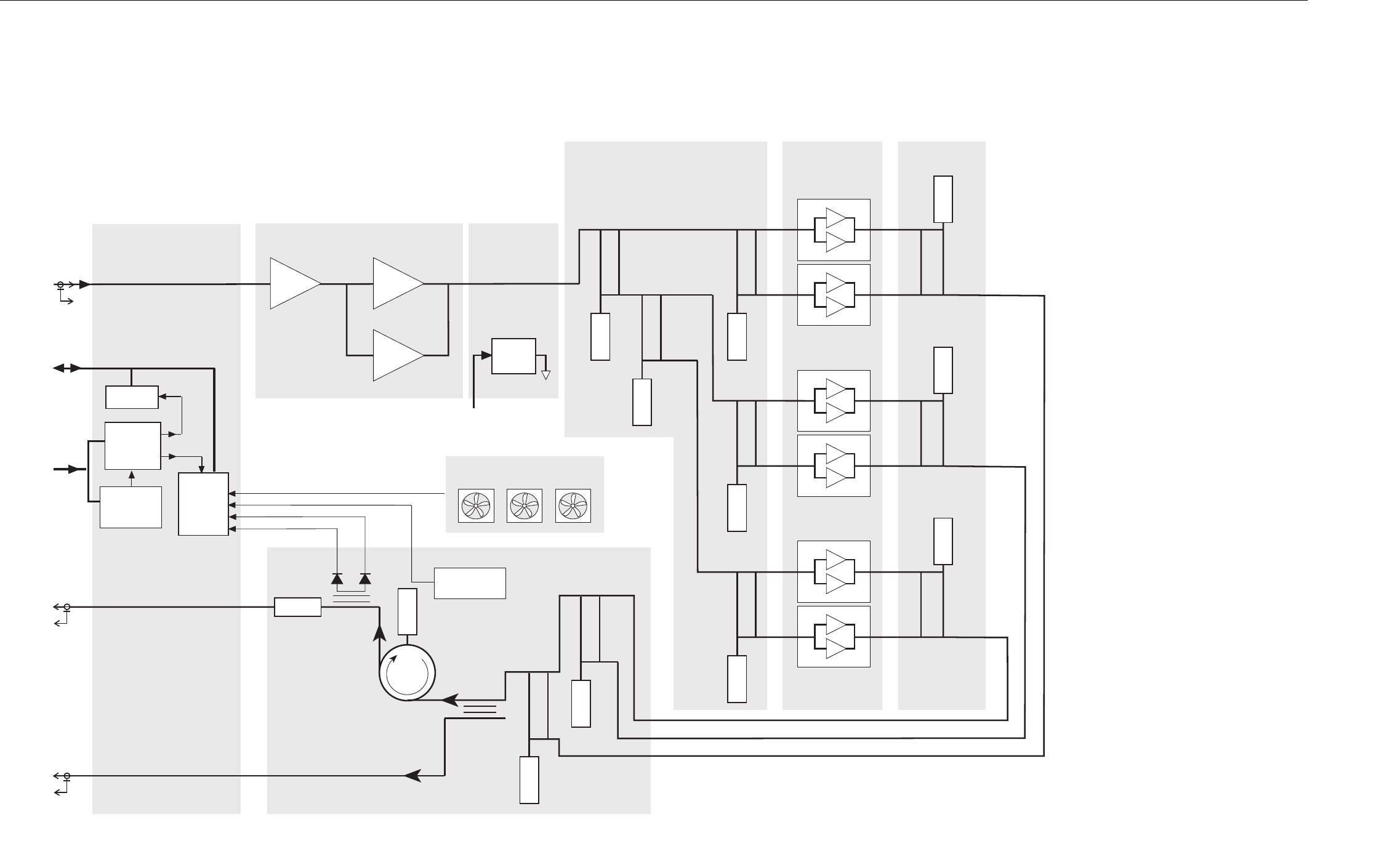
4-16
68P81095E02-D 4/1/2000
800/900/1500 MHz Base Radios EBTS System Manual - Vol 2
Power Amplifier
COMBINER
BOARD
LINEAR DRIVER MODULE
LINEAR FINAL
MODULES
50 OHM
LOAD
ADDRESS BUS
FROM BRC
SPI BUS
TO/FROM BRC
ADDRESS DECODE, MEMORY,
& A/D CONVERTER CIRCUITRY
MEMORY
A/D
CONVERTER
BOARD SELECT
DECODE
CIRCUITRY
PA TEMP SENSE
CHIP
SELECT
CHIP SELECT
DECODE
CIRCUITRY
CHIP SELECT
RF COMBINER/
PERIPHERAL MODULE
LOW-PASS
FILTER
RF INPUT
RF OUT
TO ANTENNA
RF FEEDBACK
TO EXCITER
MODULE
REF PWR
FWD PWR
FAN SENSE
FAN ASSEMBLY
TEMPERATURE
SENSOR
EBTS417
120497JNM
CLK/DATA
CIRCULATOR
50 OHM
LOAD
50 OHM
LOAD
50 OHM
LOAD
50 OHM
LOAD
50 OHM
LOAD
50 OHM
LOAD
STAGE
1
CLASS AB STAGE 2
CLASS AB
RF SPLITTER/DC DISTRIBUTION BOARD
INTERCONNECT
BOARD
STAGE 3
CLASS AB
50 OHM
LOAD
50 OHM
LOAD
50 OHM
LOAD
50 OHM
LOAD
DC
FILTER
+28 VDC
Figure:4-6
TLN3335 (CTF1040) 70 W, 800 MHz Power Amplifier
Functional Block Diagram (Sheet 1 of 1)
70W, 800 MHz Power Amplifier – TLN3335 (CTF1040)
Functional Block Diagram
68P81095E02-D 4/1/2000
4-17
EBTS System Manual - Vol 2 800/900/1500 MHz Base Radios
Power Amplifier
LINEAR DRIVER MODULE RF SPLITTER/
DC DISTRIBUTION BOARD
50 OHM
LOAD
LINEAR FINAL MODULE
50 OHM
LOAD
LINEAR FINAL MODULE
50 OHM
LOAD
ADDRESS BUS
FROM BRC
SPI BUS
TO/FROM BRC
ADDRESS DECODE, MEMORY,
& A/D CONVERTER CIRCUITRY
MEMORY
A/D
CONVERTER
BOARD SELECT
DECODE
CIRCUITRY
PA TEMP SENSE
CHIP
SELECT
CHIP SELECT
DECODE
CIRCUITRY
CHIP SELECT
RF COMBINER/
PERIPHERAL MODULE
LOW-PASS
FILTER
RF INPUT
RF OUT
TO ANTENNA
RF FEEDBACK
TO EXCITER
MODULE
REF PWR
FWD PWR
FAN SENSE
FAN ASSEMBLY
TEMPERATURE
SENSOR
EBTS326
011497JNM
CLK/DATA
CIRCULATOR
50 OHM
LOAD
50 OHM
LOAD 50 OHM
LOAD
STAGE
1STAGE
3
STAGE
2
CLASS A CLASS AB CLASS AB
50 OHM
LOAD
Figure:4-7
60W, 900 MHz Power Amplifier Functional Block Diagram
(Sheet 1 of 1)
60W, 900 MHz Power Amplifier – CLN1355 (CLF1300)
Functional Block Diagram
4-18
68P81095E02-D 4/1/2000
800/900/1500 MHz Base Radios EBTS System Manual - Vol 2
Power Amplifier
Power Amplifier
Functional Block Diagram
Model TLN3426
LINEAR DRIVER MODULE
TLG4020
STAGE
1STAGE
3STAGE
4
RF SPLITTER/
DC DISTRIBUTION BOARD
TLG4023
50 OHM
LOAD
STAGE
2(Q5433)
LINEAR FINAL MODULE
TLG4021
(Q5433)
50 OHM
LOAD
50 OHM
LOAD
(Q5417)
LINEAR FINAL MODULE
TLG4021
(Q5417)
50 OHM
LOAD
50 OHM
LOAD
ADDRESS BUS
FROM BRC
SPI BUS
TO/FROM BRC
ADDRESS DECODE, MEMORY,
& A/D CONVERTER CIRCUITRY
MEMORY
(U5004)
A/D
CONVERTER
(U5100)
BOARD SELECT
DECODE
CIRCUITRY
(U5000)
PA TEMP SENSE
CHIP
SELECT
CHIP SELECT
DECODE
CIRCUITRY
(U5000)
CHIP SELECT
RF COMBINER/
PERIPHERAL MODULE
TLG4022
50 OHM
LOAD
LOW-PASS
FILTER
RF INPUT
RF OUT
TO ANTENNA
RF FEEDBACK
TO EXCITER
MODULE
REF PWR
FWD PWR
50 OHM
LOAD
CIRCULATOR
FAN SENSE
LDM/LFM CURRENT SENSE
FAN ASSEMBLY
FAN FANFAN
LFM CURRENT SENSE
LDM CURRENT SENSE
TEMPERATURE
SENSOR
(RT5401)
CLASS A CLASS AB CLASS AB CLASS AB
Figure:4-8
Power
Amplifier
40W, 1500 MHz Power Amplifier – TLN3426
Functional Block Diagram
68P81095E02-D 11/9//2000
4-19
EBTS System Manual - Vol 2 800/900/1500 MHz Base Radios
Power Amplifier
4
COMBINER
BOARD
LINEAR DRIVER MODULE
LINEAR FINAL
MODULES
50 OHM
LOAD
ADDRESS BUS
FROM BRC
SPI BUS
TO/FROM BRC
ADDRESS DECODE, MEMORY,
& A/D CONVERTER CIRCUITRY
MEMORY
A/D
CONVERTER
BOARD SELECT
DECODE
CIRCUITRY
PA TEMP SENSE
CHIP
SELECT
CHIP SELECT
DECODE
CIRCUITRY
CHIP SELECT
RF COMBINER/
PERIPHERAL MODULE
LOW-PASS
FILTER
RF INPUT
RF OUT
TO ANTENNA
RF FEEDBACK
TO EXCITER
MODULE
REF PWR
FWD PWR
FAN SENSE
FAN ASSEMBLY
TEMPERATURE
SENSOR
EBTS417
120497JNM
CLK/DATA
CIRCULATOR
50 OHM
LOAD
50 OHM
LOAD
50 OHM
LOAD
50 OHM
LOAD
50 OHM
LOAD
50 OHM
LOAD
STAGE
1
CLASS AB STAGE 2
CLASS AB
RF SPLITTER/DC DISTRIBUTION BOARD
INTERCONNECT
BOARD
STAGE 3
CLASS AB
50 OHM
LOAD
50 OHM
LOAD
50 OHM
LOAD
50 OHM
LOAD
DC
FILTER
+28 VDC
Figure:4-9
QUAD Channel Power Amplifier Functional Block
Diagram (Sheet 1 of 1)
800 MHz QUAD Carrier Power Amplifier
Functional Block Diagram
DUAL Stage Isolator

This Page Intentionally
Left Blank
4-20
68P81095E02-D 11/9//2000
800/900/1500 MHz Base Radios EBTS System Manual - Vol 2
Power Amplifier

68P81095E02-D 11/9/2000
5-21
EBTS System Manual - Vol 2 800/900/1500 MHz Base Radios
5 DC Power Supply
Overview
This section provides technical information for the DC Power Supply (PS). Table
5-1 describes covered topics.
FRU Number to Kit Number Cross Reference
DC Power Supply Field Replaceable Units (FRUs) are available for the iDEN
EBTS. The FRU contains the Power Supply kit and required packaging. Table 5-2
provides a cross reference between Exciter FRU numbers and kit numbers.
Table 5-1
Chapter Topics
Chapter Page Description
DC Power Supply for Single Channel Base Radios 5-22 Describes the functions and characteristics of the DC Power
Supply (PS) module for the single channel Base Radio (BR).
Single Channel DC Power Supply 5-29 Describes the functions and characteristics of the DC Power
Supply (PS) module for the QUAD channel Base Radio (BR).
Single Channel DC Power Supply 5-30 Functional Block Diagram for the Single Channel DC Power
Supply (PS)
QUAD Channel Power Supply 5-31 Functional Block Diagram for the QUAD Channel DC Power
Supply (PS)
Table 5-2
FRU Number to Kit Number Cross Referece
Description FRU Number Kit Number
Single Channel DC Power Supply TLN3338 CPN1027
QUAD Channel DC Power Supply CLN1498 CLF1550

5-22
68P81095E02-D 4/16/99
800/900/1500 MHz Base Radios EBTS System Manual - Vol 2
DC Power Supply for Single Channel Base Radios
DC Power Supply for Single Channel
Base Radios
DC Power Supply Overview
The DC Power Supply provides DC operating voltages to QUAD Channel Base
Radio FRUs. The power supply accepts input voltage sources from 41Vdc to
60Vdc. Input sources may be either positively or negatively grounded.
On initial startup, the supply requires a nominal 43 Vdc. If the voltage drops
below 41 V, the DC Power Supply enters quiescent mode. In quiescent mode, the
power supply outputs no power.
The DC Power Supply is designed for sites with an available DC voltage source.
Output voltages from the DC Power Supply are 28.6 Vdc, 14.2 Vdc and 5.1 Vdc,
with reference to output ground. The supply is rated for 575 Watts of continuous
output power, with up to 113û F (45û C) inlet air. At 140û F (60û C), the 28.6 Vdc
output reduces to 80% of maximum power.
The DC Power Supply consists of the Power Supply and front panel hardware.
The DC Power Supply connects to the chassis backplane through an edgecard
connector. Two Torx screws on the front panel secure the DC power supply to the
chassis.
Figure 5-1 shows the DC Power Supply with the cover removed.
Controls and Indicators
Table 5-3 summarizes LED indications on the DC Power Supply during normal
operation. The ON/OFF switch behind the front panel turns DC power supply on
and off.
Performance Specifications
Table 5-4 lists the speciÞcations for the DC Power Supply.
Table 5-3
DC Power Supply Indicators
LED Condition Indications
Green Solid (on) Power Supply is on, and operating under normal conditions with
no alarms
Off Power Supply is turned off or required power is not available
Red Solid (on) Power Supply fault or load fault on any output, or input voltage is
out of range
Off Power Supply is operating normally, with no alarms
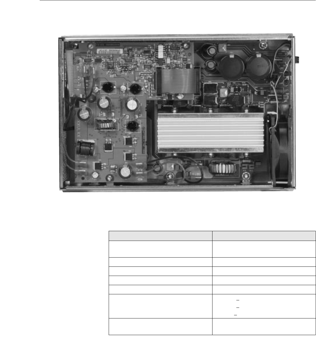
68P81095E02-D 11/9/2000
5-23
EBTS System Manual - Vol 2 800/900/1500 MHz Base Radios
DC Power Supply for Single Channel Base Radios
Table 5-4
DC Power Supply Specifications
Description Value or Range
Operating Temperature 0¡ to +40¡ C (no derating)
+41¡ to +60¡ C (derating)
Input Voltage 41 to 60 Vdc
Input Polarity Positive (+) ground system
Startup Voltage 43 Vdc (minimum)
Input Current 15.6 A (maximum) @ 41 Vdc
Steady State Output Voltages 28.6 Vdc +5%
14.2 Vdc +5%
5.1 Vdc +5%
Total Output Power Rating 575 W (no derating)
485 W (derating)
Figure:5-1
DC Power Supply

5-24
68P81095E02-D 4/16/99
800/900/1500 MHz Base Radios EBTS System Manual - Vol 2
DC Power Supply for Single Channel Base Radios
Theory of Operation
Table 5-5 brießy describes the basic DC Power Supply circuitry. Figure 5-3 shows
the functional block diagrams for the DC Power Supply.
Output Ripple All outputs 50mV p-p (measured with
20 MHz BW oscilloscope at 25¡C)
High Frequency individual harmonic voltage
limits (10kHz to 100MHz) are:
28.6 Vdc 1.5 mV p-p
14.2 Vdc 3.0 mV p-p
5.1 Vdc 5.0 mV p-p
Short Circuit Current 0.5 A average (maximum)
Table 5-5
DC Power Supply Circuitry
Circuit Description
Input Circuit Routes input current from the DC power input cable through the
high current printed circuit edge connector, EMI Þlter, panel mounted
combination circuit breaker, and on/off switch
Startup Inverter
Circuitry
Provides Vdc for power supply circuitry during initial power-up
Main Inverter Circuitry Consists of a switching-type power supply to generate the +28.6 Vdc
supply voltage
Temperature Protection The Power Supply contains a built-in cooling fan that runs whenever
the supply is powered on. The supply shuts down if the temperature
exceeds a preset threshold
+14.2 Vdc Secondary
Converter Circuitry
Consists of a switching-type power supply to generate the +14.2 Vdc
supply voltage
+5 Vdc Secondary
Converter Circuitry
Consists of a switching-type power supply to generate the +5.1 Vdc
supply voltage
Clock Generator
Circuitry
Generates the 267 kHz and 133 kHz clock signals used by the pulse
width modulators in the four inverter circuits
Address Decode,
Memory, & A/D
Converter
Serves as the main interface between A/D on the Power Supply and
the BRC via the SPI bus
Table 5-4
DC Power Supply Specifications (Continued)
Description Value or Range

68P81095E02-D 11/9/2000
5-25
EBTS System Manual - Vol 2 800/900/1500 MHz Base Radios
DC Power Supply for QUAD Channel Base Radios
DC Power Supply for QUAD Channel
Base Radios
QUAD Channel Power Supply Overview
The QUAD Channel DC Power Supply provides DC operating voltages to QUAD
Channel Base Radio FRUs. The power supply accepts input voltage sources from
41Vdc to 60Vdc. Input sources may be either positively or negatively grounded.
On initial startup, the supply requires a nominal 43 Vdc. If the voltage drops
below 41 V, the QUAD Channel DC Power Supply enters quiescent mode. In
quiescent mode, the power supply outputs no power.
The QUAD Channel DC Power Supply is designed for sites with an available DC
voltage source. Output voltages from the DC Power Supply are 28.6 Vdc, 14.2 Vdc
and 3.3 Vdc, with reference to output ground. The supply is rated for 575 Watts of
continuous output power, with up to 113û F (45û C) inlet air. At 140û F (60û C), the
28.6 Vdc output reduces to 80% of maximum power.
The QUAD Channel DC Power Supply consists of the Power Supply and front
panel hardware. The QUAD Channel DC Power Supply connects to the chassis
backplane through an edgecard connector. Two Torx screws on the front panel
secure the QUAD Channel DC power supply to the chassis.
Figure 5-2 shows the QUAD Channel Power Supply with the cover removed.
Controls and Indicators
Table 5-6 summarizes LED indications on the QUAD Channel DC Power Supply
during normal operation. The ON/OFF switch behind the front panel turns DC
power supply on and off.
Performance Specifications
Table 5-7 lists the speciÞcations for the QUAD Channel DC Power Supply.
Table 5-6
DC Power Supply Indicators
LED Condition Indications
Green Solid (on) Power Supply is on, and operating under normal conditions with
no alarms
Off Power Supply is turned off or required power is not available
Red Solid (on) Power Supply fault or load fault on any output, or input voltage is
out of range
Off Power Supply is operating normally, with no alarms
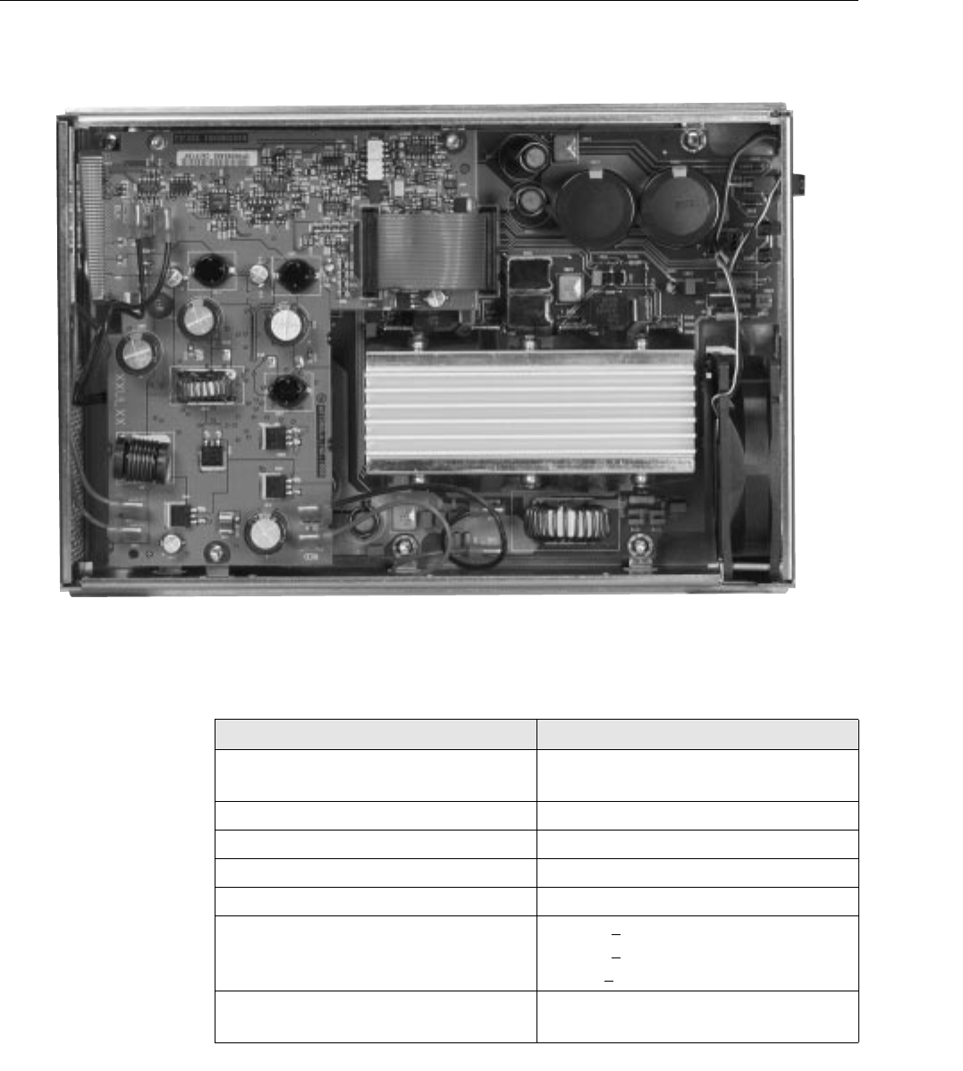
5-26
68P81095E02-D 4/16/99
800/900/1500 MHz Base Radios EBTS System Manual - Vol 2
DC Power Supply for QUAD Channel Base Radios
Table 5-7
DC Power Supply Specifications
Description Value or Range
Operating Temperature 0¡ to +40¡ C (no derating)
+41¡ to +60¡ C (derating)
Input Voltage 41 to 60 Vdc
Input Polarity Positive (+) ground system
Startup Voltage 43 Vdc (minimum)
Input Current 18.0 A (maximum) @ 41 Vdc
Steady State Output Voltages 28.6 Vdc +5%
14.2 Vdc +5%
3.3 Vdc +5%
Total Output Power Rating 575 W (no derating)
485 W (derating)
Figure:5-2
Quad Carrier Power Supply

68P81095E02-D 11/9/2000
5-27
EBTS System Manual - Vol 2 800/900/1500 MHz Base Radios
DC Power Supply for QUAD Channel Base Radios
Theory of Operation
Table 5-8 brießy describes the basic DC Power Supply circuitry. Figure 5-5 shows
the functional block diagrams for the DC Power Supply.
Output Ripple All outputs 150mV p-p (measured with
20 MHz BW oscilloscope at 25¡C)
High Frequency individual harmonic voltage
limits (10kHz to 100MHz) are:
28.6 Vdc 1.5 mV p-p
14.2 Vdc 3.0 mV p-p
3.3 Vdc 5.0 mV p-p
Short Circuit Current 0.5 A average (maximum)
Table 5-8
DC Power Supply Circuitry
Circuit Description
Input Circuit Routes input current from the DC power input cable through the
high current printed circuit edge connector, EMI Þlter, panel mounted
combination circuit breaker, and on/off switch
Startup Inverter
Circuitry
Provides Vdc for power supply circuitry during initial power-up
Main Inverter Circuitry Consists of a switching-type power supply to generate the +28.6 Vdc
supply voltage
Temperature Protection The Power Supply contains a built-in cooling fan that runs whenever
the supply is powered on. The supply shuts down if the temperature
exceeds a preset threshold
+14.2 Vdc Secondary
Converter Circuitry
Consists of a switching-type power supply to generate the +14.2 Vdc
supply voltage
+3.3 Vdc Secondary
Converter Circuitry
Consists of a switching-type power supply to generate the +3.3 Vdc
supply voltage
Clock Generator
Circuitry
Generates the 267 kHz and 133 kHz clock signals used by the pulse
width modulators in the four inverter circuits
Address Decode,
Memory, & A/D
Converter
Serves as the main interface between A/D on the Power Supply and
the BRC via the SPI bus
Table 5-7
DC Power Supply Specifications (Continued)
Description Value or Range

5-28
68P81095E02-D 11/9/2000
800/900/1500 MHz Base Radios EBTS System Manual - Vol 2
This Page Intentionally
Left Blank
68P81095E02-D 11/9/2000
5-29
EBTS System Manual - Vol 2 800/900/1500 MHz Base Radios
DC Power Supply
5
Single Channel DC Power Supply
+5.1 V INVERTER CIRCUITRY
FET
DRIVER
POWER FET
SWITCH FILTER
CIRCUITRY
VCC
VCC
+ 5V OVERCURRENT
DETECT
REF
REF
SURGE CURRENT
DELAY REF
OVERVOLTAGE
DETECT
FET
CROWBAR
CIRCUIT
+ 28V BULK
PULSE
WIDTH
MODULATOR
A
24
25
30
31
+5.1 V DC
TO
STATION
MODULES
VIA
BACKPLANE
P/O
BACKPLANE
CONNECTOR
+5.1 V
÷ 2
CLOCK GENERATOR CIRCUITRY
STARTUP INVERTER CIRCUITRY
BULK DETECT
TO
DIAGNOSTICS
CIRCUITRY
PULSE
WIDTH
MODULATOR
VCC
VCC STARTUP ISOLATION
TRANSFORMER
+14.2 V INVERTER CIRCUITRY
FET
DRIVER
POWER FET
SWITCH FILTER
CIRCUITRY
VCC
VCC
+ 14.2V OVERCURRENT
DETECT
REF
REF
SURGE CURRENT
DELAY REF
OVERVOLTAGE
DETECT
FET
CROWBAR
CIRCUIT
A
16
17
22
23
+14.2V DC
TO
STATION
MODULES
VIA
BACKPLANE
P/O
BACKPLANE
CONNECTOR
+14.2V
+14.2V
PULSE
WIDTH
MODULATOR
PULSE
WIDTH
MODULATOR
FRONT PANEL
ON / OFF
SWITCH
EXTERNAL
DC INPUT
41-60 VDC
FILTER
CIRCUITRY
INPUT FILTER BOARD
3
4
14
15
+28.6 VDC
TO
STATION
MODULES
VIA
BACKPLANE
P/O
BACKPLANE
CONNECTOR
MAIN INVERTER CIRCUITRY
REF
REF
CURRENT
DETECT A
+28.6 V OVERVOLTAGE
DETECT
+28 V BULK TO
DIAGNOSTICS
CIRCUITRY
OVERCURRENT
DETECT
+28.6 VDC
CLOCK
GENERATOR
CIRCUITRY
267 KHZ
TRANSISTOR
SWITCH
B
MAIN ISOLATION
TRANSFORMER
TRANSISTOR
DRIVERS
SOFTSTART
CIRCUITRY
SHUTDOWN
A
+12V STARTUP BIAS
+12V STARTUP BIAS
VCC
VCC
MOD FAIL
133 KHZ
267 KHZ
133 KHZ
133 KHZ
133 KHZ
133 KHZ
133 KHZ
267 KHZ
133 KHZ
267 KHZ
133 KHZ
POWER FET
SWITCHES FILTERING
CIRCUITRY
+28 V BULK
EBTS323
011497JNM
Figure:5-3
DC Power Supply Functional Block Diagram
(Sheet 1 of 2)

5-30
68P81095E02-D 11/9/2000
800/900/1500 MHz Base Radios EBTS System Manual - Vol 2
DC Power Supply
A/D
CONVERTER
COOLING
FAN
THERMISTOR
MOUNTED ON
HEATSINK
SPI BUS
REF
REF
REF
MOD FAIL
INPUT FAIL
HEATSINK DIAG
VBAT DIAG
BAT TEMP
+5.1 V
+14.2V DIAG
+5.1 V DIAG
+28.6 V DIAG
REF
REF
HEATSINK STATUS
DETECT
HI-TEMP
DETECT
BULK DETECT
FROM STARTUP
INVERTER
CIRCUITRY
(FOR AC ONLY)
FROM BATTERY
CHARGER/REVERT
CIRCUITRY
FROM
DETECT
CIRCUITRY
A
B
INPUT GOOD
(GREEN)
MODULE
FAIL
(RED)
3
SPI BUS
TO/FROM
STATION CONTROL
MODULE
ADDRESS DECODE CIRCUITRY
ADDRESS
DECODE
CIRCUITRY
FROM
STATION
CONTROL
BOARD 9
P/O ADDRESS BUS ENABLE ENABLE
DIAGNOSTICS CIRCUITRY
T°
EBTS324
012097JNM
J300
REF
DC Power Supply
Figure:5-4
DC Power Supply Functional Block Diagram
(Sheet 2 of 2)
5-31
68P81095E02-D 11/9/2000
800/900/1500 MHz Base Radios EBTS System Manual - Vol 2
DC Power Supply
Figure:5-5
QUAD Channel DC Power Supply Functional Block
Diagram
(Sheet 1 of 2)
QUAD Channel Power Supply
+3.3 V INVERTER CIRCUITRY
FET
DRIVER
POWER FET
SWITCH FILTER
CIRCUITRY
VCC
VCC
+ 3.3V OVERCURRENT
DETECT
REF
REF
SURGE CURRENT
DELAY REF
OVERVOLTAGE
DETECT
FET
CROWBAR
CIRCUIT
+ 28V BULK
PULSE
WIDTH
MODULATOR
A
24
25
30
31
+3.3 V DC
TO
STATION
MODULES
VIA
BACKPLANE
P/O
BACKPLANE
CONNECTOR
+3.3 V
÷ 2
CLOCK GENERATOR CIRCUITRY
STARTUP INVERTER CIRCUITRY
BULK DETECT
TO
DIAGNOSTICS
CIRCUITRY
PULSE
WIDTH
MODULATOR
VCC
VCC STARTUP ISOLATION
TRANSFORMER
+14.2 V INVERTER CIRCUITRY
FET
DRIVER
POWER FET
SWITCH FILTER
CIRCUITRY
VCC
VCC
+ 14.2V OVERCURRENT
DETECT
REF
REF
SURGE CURRENT
DELAY REF
OVERVOLTAGE
DETECT
FET
CROWBAR
CIRCUIT
A
16
17
22
23
+14.2V DC
TO
STATION
MODULES
VIA
BACKPLANE
P/O
BACKPLANE
CONNECTOR
+14.2V
+14.2V
PULSE
WIDTH
MODULATOR
PULSE
WIDTH
MODULATOR
FRONT PANEL
ON / OFF
SWITCH
EXTERNAL
DC INPUT
41-60 VDC
FILTER
CIRCUITRY
INPUT FILTER BOARD
3
4
14
15
+28.6 VDC
TO
STATION
MODULES
VIA
BACKPLANE
P/O
BACKPLANE
CONNECTOR
MAIN INVERTER CIRCUITRY
REF
REF
CURRENT
DETECT A
+28.6 V OVERVOLTAGE
DETECT
+28 V BULK TO
DIAGNOSTICS
CIRCUITRY
OVERCURRENT
DETECT
+28.6 VDC
CLOCK
GENERATOR
CIRCUITRY
267 KHZ
TRANSISTOR
SWITCH
B
MAIN ISOLATION
TRANSFORMER
TRANSISTOR
DRIVERS
SOFTSTART
CIRCUITRY
SHUTDOWN
A
+12V STARTUP BIAS
+12V STARTUP BIAS
VCC
VCC
MOD FAIL
133 KHZ
267 KHZ
133 KHZ
133 KHZ
133 KHZ
133 KHZ
133 KHZ
267 KHZ
133 KHZ
267 KHZ
133 KHZ
POWER FET
SWITCHES FILTERING
CIRCUITRY
+28 V BULK
EBTS323Q
101900 spf
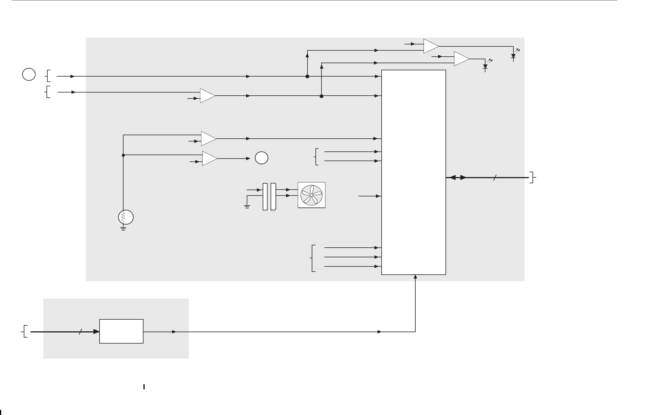
5-32
68P81095E02-D 11/9/2000
800/900/1500 MHz Base Radios EBTS System Manual - Vol 2
DC Power Supply
Figure:5-6
QUAD Channel DC Power Supply Functional Block Diagram
(Sheet 2 of 2)
QUAD Channel DC Power Supply
A/D
CONVERTER
COOLING
FAN
THERMISTOR
MOUNTED ON
HEATSINK
SPI BUS
REF
REF
REF
MOD FAIL
INPUT FAIL
HEATSINK DIAG
VBAT DIAG
BAT TEMP
+3.3 V
+14.2V DIAG
+3.3 V DIAG
+28.6 V DIAG
REF
REF
HEATSINK STATUS
DETECT
HI-TEMP
DETECT
U
LK DETECT
O
M STARTUP
INVERTER
C
IRCUITRY
(FOR AC ONLY)
FROM BATTERY
CHARGER/REVERT
CIRCUITRY
FROM
DETECT
CIRCUITRY
A
B
INPUT GOOD
(GREEN)
MODULE
FAIL
(RED)
3
SPI BUS
TO/FROM
STATION CONTROL
MODULE
ADDRESS DECODE CIRCUITRY
ADDRESS
DECODE
CIRCUITRY
9
P/O ADDRESS BUS ENABLE ENABLE
DIAGNOSTICS CIRCUITRY
T°
EBTS324Q
101900spf
J300
REF

68P81095E02-D 4/1/2000
6-33
EBTS System Manual - Vol 2 800/900/1500 MHz Base Radios
6 AC Power Supply
AC Power Supply Overview
The AC Power Supply provides DC operating voltages for the Base Radio FRUs.
The AC Power Supply accepts an AC input (90 to 280 Vac @ 47 to 63 Hz) to
generate three output voltages: 28.6 Vdc, 14.2 Vdc and 5.1 Vdc with reference to
output ground. The AC Power Supply automatically adjusts to the AC input
ranges and supplies a steady output.
The AC Power Supply contains several switching-type power supply circuits,
power factor correction circuitry, battery charger/revert circuitry, diagnostics and
monitoring circuitry.
The battery charging/revert circuitry charges an external storage battery and
automatically reverts to battery power in case of an AC power failure.
The Power Supply interconnects to the chassis backplane using an edgecard
connector. Two Torx screws on the front panel of the AC Power Supply secure it
in the chassis.
Figure 6-1 shows the front view of the AC Power Supply.
Controls and Indicators
Table 6-1 lists and describes the indicators of the AC Power Supply. The power
ON/OFF switch is used to turn the power supply on and off.
Performance Specifications
Table 6-2 lists the speciÞcations for the AC Power Supply.
Table 6-1
AC Power Supply Indicators
LED Condition Indications
Green Solid (on) Power Supply under normal operation with no alarms (the red
LED is normally off when this LED is lit)
Off Power Supply is turned off or required power is not available
Red Solid (on) In battery revert mode, Power Supply fault, or load fault on any
output
Off The Power Supply is under normal operation with no alarms
6-34
68P81095E02-D 4/1/2000
800/900/1500 MHz Base Radios EBTS System Manual - Vol 2
Table 6-2
AC Power Supply Specifications
Description Value or Range
Operating Temperature -30¡ to +45¡ C (no derating)
-30¡ to +60¡ C (derating)
Input Voltage 90 to 280 Vac
Input Frequency Range 47 to 63 Hz
Input Current 8.5 A (maximum)
Steady State Output Voltages 28.6 Vdc +5%
14.2 Vdc +5%
5.1 Vdc +5%
Total Output Power Rating 625 W (no derating)*
595 W (derating)*
Battery Charging Voltage Range 26 to 32.5 Vdc
Figure:6-1
AC Power Supply (front view)

68P81095E02-D 4/1/2000
6-35
EBTS System Manual - Vol 2 800/900/1500 MHz Base Radios
Theory of Operation
Table 6-3 brießy describes the basic AC Power Supply circuitry. Figure 6-2 shows
the functional block diagrams for the AC Power Supply.
Output Ripple All outputs 50 mV p-p (measured with 20 MHz BW
oscilloscope at 25¡C)
High Frequency individual harmonic voltage limits
(10 kHz to 100 MHz) are:
28.6 Vdc 1.5 mV p-p
14.2 Vdc 3 mV p-p
5.1 Vdc 5 mV p-p
Short Circuit Current 0.5 A average (maximum)
* Includes 50 W for the battery charger.
Table 6-3
AC Power Supply Circuitry
Circuit Description
Input Conditioning
Circuitry
Consists of ac line transient protection, EMI Þltering, rectiÞer, power
factor correction circuitry, and Þltering
Start-up Inverter
Circuitry
Provides Vcc for power supply circuitry during initial power-up
Main Inverter Circuitry Consists of a switching-type power supply to generate the +28.6Vdc
supply voltage
Temperature Protection Contains a built-in thermostatically controlled cooling fan. The
Power Supply shuts down if temperature exceeds a preset threshold
+14.2 Vdc Secondary
Converter Circuitry
Consists of a switching-type power supply to generate the +14.2 Vdc
supply voltage
+5 Vdc Secondary
Converter Circuitry
Consists of a switching-type power supply to generate the +5 Vdc
supply voltage
Clock Generator
Circuitry
Generates 267 kHz and 133 kHz clock signals for the pulse width
modulators in the four inverter circuits
Diagnostics Circuitry Converts analog status signals to digital format for transfer to BRC
Address Decode,
Memory, & A/D
Converter
Serves as the main interface between A/D and D/A on the Power
Supply and the BRC via the SPI bus
Battery Charging/
Revert Circuitry
Offers features such as output short circuit protection, reversed
battery protection, ambient battery temperature monitoring, and
immediate revert to battery backup leaving no interruption of station
operation
In the event of an AC power failure, a battery revert relay is energized
which places the storage battery on the +28 V bus which maintains
station operation under backup power. An SCR in parallel with the
relay contacts provides instant battery revert and protection for the
relay contacts against arcing
Table 6-2
AC Power Supply Specifications
Description Value or Range

6-36
68P81095E02-D 4/1/2000
800/900/1500 MHz Base Radios EBTS System Manual - Vol 2
This Page Intentionally
Left Blank
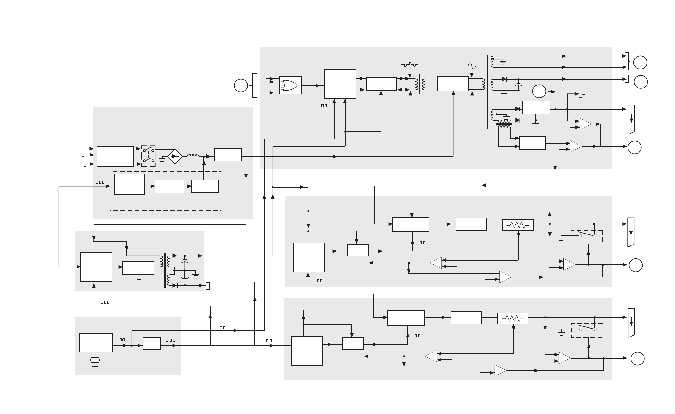
68P81095E02-D 4/1/2000
6-37
EBTS System Manual - Vol 2 800/900/1500 MHz Base Radios
AC Power Supply
6
6
CLOCK GENERATOR CIRCUITRY
STARTUP INVERTER CIRCUITRY
BULK DETECT
TO
DIAGNOSTICS
CIRCUITRY
VCC
VCC STARTUP ISOLATION
TRANSFORMER
FRONT PANEL
ON / OFF
SWITCH
AC INPUT
47 - 60 HZ
90V / 280V AC
INPUT FILTER BOARD
3
4
14
15
+28.6 VDC
TO
STATION
MODULES
VIA
BACKPLANE
P/O
BACKPLANE
CONNECTOR
MAIN INVERTER CIRCUITRY
REF
REF
A
+28.6 V OVERVOLTAGE
DETECT
+28 V BULK TO
DIAGNOSTICS
CIRCUITRY
OVERCURRENT
DETECT
+28.6 VDC
TRANSISTOR
SWITCH
B
MAIN ISOLATION
TRANSFORMER
SOFTSTART
CIRCUITRY
SHUTDOWN
A
+12V STARTUP BIAS
+12V STARTUP BIAS
VCC
VCC
MOD FAIL
133 KHZ
133 KHZ
133 KHZ
267 KHZ
133 KHZ
267 KHZ
133 KHZ
CLOCK
GENERATOR
CIRCUITRY
267 KHZ
PULSE
WIDTH
MODULATOR
+5.1V INVERTER CIRCUITRY
VCC VCC
+ 5V OVERCURRENT
DETECT
REF
REF
SURGE CURRENT
DELAY REF
OVERVOLTAGE
DETECT
FET
CROWBAR
CIRCUIT
+ 28V BULK
A
24
25
30
31
+5.1V DC
TO
STATION
MODULES
VIA
BACKPLANE
P/O
BACKPLANE
CONNECTOR
+5.1V
133 KHZ
FILTER
CIRCUITRY
POWER FET
SWITCH
FET
DRIVER
PULSE
WIDTH
MODULATOR
+14.2 V INVERTER CIRCUITRY
VCC VCC
+ 14.2V OVERCURRENT
DETECT
REF
REF
SURGE CURRENT
DELAY REF
OVERVOLTAGE
DETECT
FET
CROWBAR
CIRCUIT
A
16
17
22
23
+14.2V DC
TO
STATION
MODULES
VIA
BACKPLANE
P/O
BACKPLANE
CONNECTOR
+14.2V
133 KHZ
FILTER
CIRCUITRY
POWER FET
SWITCH
FET
DRIVER
PULSE
WIDTH
MODULATOR
+14.2V
133 KHZ
PULSE
WIDTH
MODULATOR
TRANSISTOR
DRIVERS
CURRENT
DETECT
FILTERING
CIRCUITRY
POWER FET
SWITCHES
267 KHZ
FILTER
CIRCUITRY
FULL WAVE
BRIDGE
RECTIFIER
FET
SWITCHES
TRANSISTOR
DRIVER
PULSE
WIDTH
MODULATOR
POWER FACTOR CORRECTION /
BOOST CONVERTER CIRCUITRY
67 KHZ
D
C
APPROX. 400 VDC
TRANSIENT / EMI
PROTECTION
CIRCUITRY
÷ 2
EBTS009
051594JNM
+ 28V BULK
Figure:6-2
AC Power Supply Functional
Block Diagram (Sheet 1 of 2)
AC Power Supply
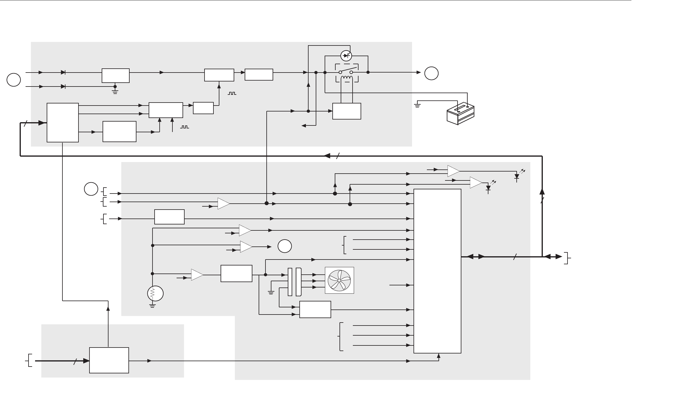
6-38
68P81095E02-D 4/1/2000
800/900/1500 MHz Base Radios EBTS System Manual - Vol 2
AC Power Supply
FAN FAULT
DETECT
FET
SWITCH
COOLING
FAN
THERMISTOR
MOUNTED ON
HEATSINK
SPI BUS
REF
REF
REF
REF
MOD FAIL
AC FAIL
28 RIPPLE
HEATSINK DIAG
VBAT DIAG
BAT TEMP
FAN ON
+5V
FAN FAIL
+14.2V DIAG
+5.1V DIAG
+28.6V DIAG
FAN CONTROL
REF
REF
HEATSINK STATUS
DETECT
HI-TEMP
DETECT
BULK DETECT
FROM STARTUP
INVERTER
CIRCUITRY
+ 28V BULK
FROM MAIN
INVERTER
CIRCUITRY
FROM BATTERY
CHARGER/REVERT
CIRCUITRY
FROM
DETECT
CIRCUITRY
A
B
AC ON
(GREEN)
MODULE
FAIL
(RED)
3
SPI BUS
TO/FROM
STATION
CONTROL
MODULE
ADDRESS DECODE CIRCUITRY
FROM
STATION
CONTROL
BOARD 9
P/O ADDRESS BUS ENABLE ENABLE
DIAGNOSTICS CIRCUITRY
T°
A/D
CONVERTER
RIPPLE
DETECT
CIRCUITRY
D/A
CONVERTER
PULSE
WIDTH
MODULATOR
FET
DRIVER
STATION
CONTROL
MODULE
FAIL DETECT
APPROX. 33 V DC
CHARGER OUTPUT
SELECT LINES
1 PPS
FROM SCM SHUTDOWN
FROM CLOCK
GENERATOR
CIRCUITRY
BATTERY CHARGING / REVERT CIRCUITRY
C
133 KHZ
133 KHZ
FILTER
CIRCUITRY
POWER FET
SWITCH
FILTERING
CIRCUITRY
SCR
AC FAIL
BATTERY
REVERT
RELAY
VBAT DIAG
TO DIAGNOSTICS
CIRCUITRY
+
_
STORAGE
BATTERY
D
ADDRESS
DECODE
CIRCUITRY
ENABLE
RELAY
CONTROL
CIRCUITRY
SPI BUS
(CLOCK & DATA)
SPI BUS
(CLOCK & DATA)
2
2
2
EBTS010
042594JNM
Figure:6-2
AC Power Supply Functional Block Diagram
(Sheet 2 of 2)
AC Power Supply

68P81095E02-D 4/1/2000
7-39
EBTS System Manual - Vol 2 800/900/1500 MHz Base Radio
7 Receiver
Overview
This section provides technical information for the Receiver (RX). Table 7-1
describes covered topics.
FRU Number to Kit Number Cross Reference
Receiver (RX) Field Replaceable Units (FRUs) are available for the iDEN EBTS.
The FRU contains the RX kit and required packaging. Table 7-2 provides a cross
reference between RX FRU numbers and kit numbers.
Table 7-1
Chapter Topics
Chapter Page Description
800 MHz 3X Receiver Ð CLN1283;
900 MHz 3X Receiver Ð CLN1356
7-40 Describes the functions and characteristics of the Receiver
(RX) module for the 800 MHz and 900 MHz single channel
Base Radio (BR).
1500 MHz Receiver Ð TLN3427 7-47 Describes the functions and characteristics of the Receiver
(RX) module module for the 1500 MHz single channel Base
Radio (BR).
800 MHz QUAD Channel Receiver Ð CLN1283; 7-51 Describes the functions and characteristics of the Receiver
(RX) module module for the 800 MHz QUAD channel Base
Radio (BR).
3X Receiver Functional Block Diagram 7-57 Functional Block Diagram for the Single Channel Base Radio
Receiver (RX)
1500 MHz Receiver Functional Block Diagram 7-58 Functional Block Diagram for the QUAD Channel Base
Radio Controller (BRC)
3X Receiver Functional Block Diagram 7-59 Functional Block Diagram for the QUAD Channel Base
Radio Receiver (RX)
Table 7-2
FRU Number to Kit Number Cross Referece
Description FRU Number Kit Number
3 branch Receiver for 800 MHz Single Channel BR CLN1283 CLF1470
3 branch Receiver for 900 MHz Single Channel BR CLN1356 CLF1480
Receiver for 1500 MHz Single Channel BR TLN3427 CRX1020
3 branch Receiver for 800 MHz QUAD Channel BR CLN1496 CLF1550
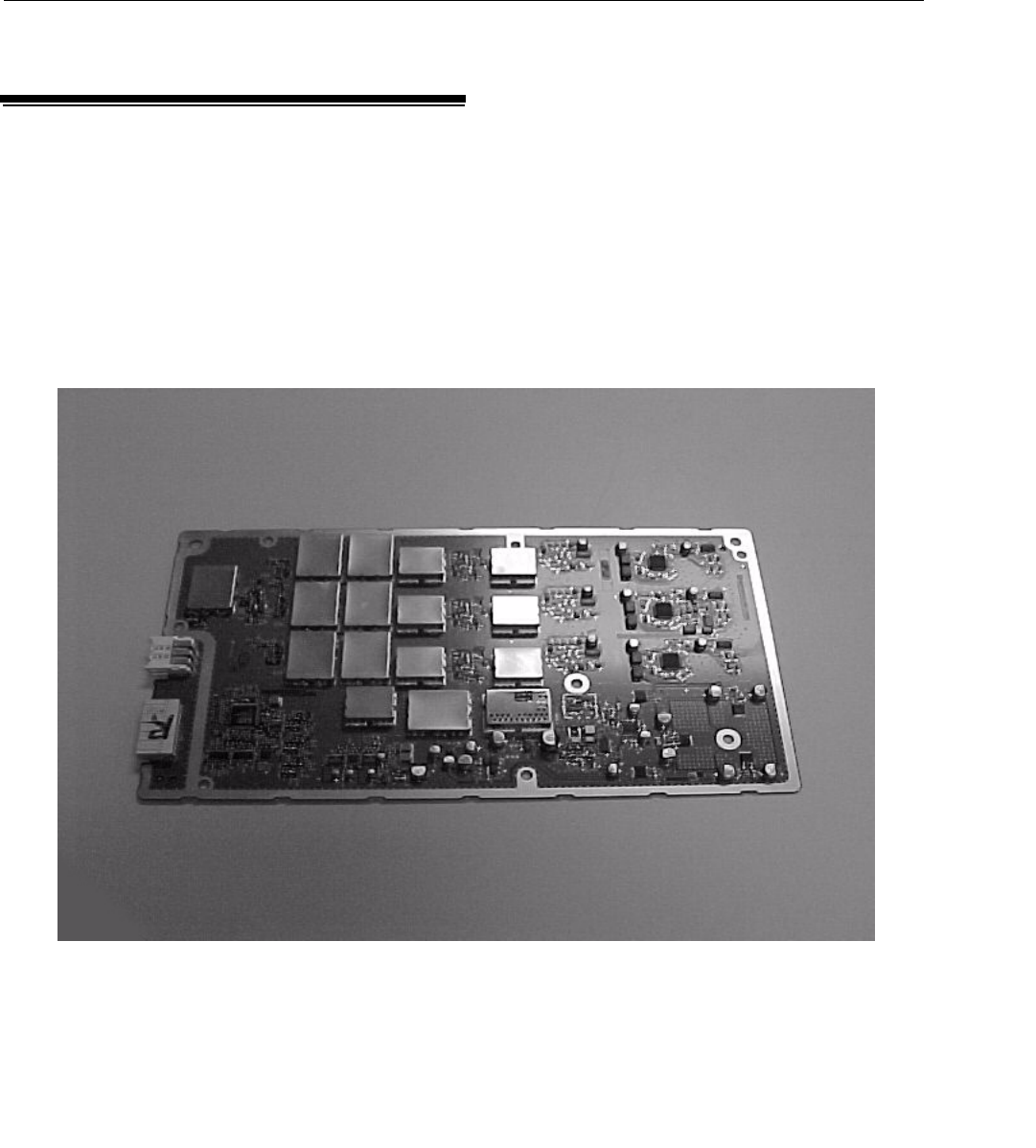
7-40
68P81095E02-D 4/1/2000
800/900/1500 MHz Base Radio EBTS System Manual - Vol 2
800 MHz 3X Receiver – CLN1283; 900 MHz 3X Receiver – CLN1356
800 MHz 3X Receiver – CLN1283;
900 MHz 3X Receiver – CLN1356
Overview
The 3X Receiver provides the receiver functions for the Base Radio. It consists of a
receiver board, a slide-in housing, and associated hardware. The 3X Receiver
incorporates one to three diversity branches on a single module. Figure 7-1 shows
a top view of the Receiver with the cover removed.
Definition and Identification
The 3X receiver kit contains three receivers on a single board. This allows a single
module to provide three-branch diversity BR functionality. To identify 3X
receiver boards in the EBTS, use the MMI command
get_rx1_kit_no
. This
command can be used on all receiver models, and reports the kit number from the
receiverÕs EEPROM. The 3X receiver can also be identiÞed by visual inspection of
the front panel. Because the 3X receiver can only be inserted into the middle
Figure:7-1
QUAD Channel Receiver (with cover removed)

68P81095E02-D 4/1/2000
7-41
EBTS System Manual - Vol 2 800/900/1500 MHz Base Radio
800 MHz 3X Receiver – CLN1283; 900 MHz 3X Receiver – CLN1356
receiver slot, the front panel of a 3X receiver reads:
INSERT ONLY IN SLOT RX2
WITH BACKPLANE 0183625X 3X RECEIVER
.
The two remaining receiver slots are covered with blank panels. A summary of
the Receiver FRUs available for the Base Radio is provided in the chart below.
Replacement Compatibility
The 3X Receiver board (CRF6010 or CRF6030) can only be used in receive slot 2
(middle receiver slot) with backplane 0183625X _ _. The backplane connector is
different than the TRF6560 version of the receiver board. This is why there is a
need for a new backplane. The receiver will function only when it is installed in
slot 2. The TRF6560 receiver will not make electrical connection in any slot of the
new backplane. Compatibility between the new and old receiver boards is
summarized in Tables 7-4 and 7-5 for 800 MHz and 900 MHz Base Radios,
respectively.
Table 7-3
Receiver FRUs
Receiver FRUs Chassis FRUs
3X Receiver:
800 MHz
900 MHz
CLN1283
CLN1356
With 3x Receiver Backplane:
800 MHz
900 MHz
CLN1282
N/A
Single Receiver:
800 MHz
900 MHz
TLN3336
N/A
With Single Receiver
Backplane:
800 MHz
900 MHz
TLN3333
N/A
Table 7-4
800 MHz Base Radio Receiver Board/BR Backplane Compatibility
CRF6010 3X Receiver TRF6560 Receiver
New backplane 0183265X-- Compatible Not compatible
Old backplane 0182416W-- Not compatible Compatible
Table 7-5
900 MHz Base Radio Receiver Board/BR Backplane Compatibility
CRF6030A 3X Receiver
New backplane 0183265X-- Compatible
Old backplane 0182416W-- Not compatible

7-42
68P81095E02-D 4/1/2000
800/900/1500 MHz Base Radio EBTS System Manual - Vol 2
800 MHz 3X Receiver – CLN1283; 900 MHz 3X Receiver – CLN1356
Diversity Configuration
There is a new software parameter used for diversity purposes with the CLN1283
and CLN1356 3X Receivers. The parameter is the
rx_fru_config
parameter. The
diversity issues to consider are described in the following paragraph. This
parameter can be accessed through the MMI commands using the Motorola
password. ROMs prior to version R06.06.17 do not support the
rx_fru_config
parameter. The ROM version in a base repeater can be checked using the MMI
command
ver
. If a repeater contains the CRF6010 or CRF6030 receiver, the BRC
board must be populated with a compatible version of ROM. Table 7-6 lists the
ROM compatibilities.
NOTE
When replacing FRUs, ensure that the ROM version
on the BRC installed in the base radio is compatible
with the ROM version on the Receiver.
NOTE
If downloaded code is used, then the downloaded
code can be used to change the needed parameter (the
rx_fru_config
parameter).
Diversity Uses and Cautions
The 3X receiver board can be used in one, two, or three branch diversity systems.
The number of active receivers is determined by the
rx_fru_config
parameter
stored on the Base Radio Control (BRC) board. The
rx_fru_config
parameter is
only valid, and must be set properly for, systems utilizing the CRF6010 or
CRF6030 3X Receiver board. The
rx_fru_config
parameter is ignored by Base
Radios that have ROM older than version R06.06.17 installed on the Base Radio
Controller board.
Table 7-6
Receiver ROM Compatibility
CRF6010/CRF6030 TRF6560
ROM version R06.03.40 Not compatible Compatible
ROM version R06.06.09 Not compatible Compatible
ROM version R06.06.17 Not compatible Compatible
ROM versions newer than R06.06.17 Compatible Compatible

68P81095E02-D 4/1/2000
7-43
EBTS System Manual - Vol 2 800/900/1500 MHz Base Radio
800 MHz 3X Receiver – CLN1283; 900 MHz 3X Receiver – CLN1356
To view the
rx_fru_config
parameter, use the MMI command
get rx_fru_config
. The conÞguration of each repeater can be changed in the
Þeld to match the number of receivers connected to antennas. To change the
rx_fru_conÞg parameter, use the command set
rx_fru_config yyy
, where yyy is
the active receiver (yyy is 1 for one branch, 12 for two branch, and 123 for three
branch diversity. For the iDEN system to work optimally, the
rx_fru_config
parameter must match the number of receivers connected to antennas.
CAUTION
There will be signiÞcant system degradation if the
rx_fru_config
parameter is not properly set in
systems with the CLN1283 or CLN1356 3X receiver
kit.
Modifying Base Radios from Three Branch to Two
Branch Diversity
NOTE
This procedure is applicable only to Base Radios
equipped with the CRF6010 or CRF6030 3X Receiver
Board.
When modifying a three branch Base Radio to a two branch Base Radio, it is
important to observe all precautionary statements in the previous paragraph.
To modify a three branch Base Radio to a two branch Base Radio:
1.
Disconnect the RF cable from the RX3 connector on the Base Radio.
2.
Connect an SMA male load (Motorola part number 5882106P03) to the RX3
connector on the Base Radio.
The SMA male load is required to limit the amount of radiated emissions.
3.
Verify that the
rx_fru_config
parameter is set properly as described in the
Diversity Uses and Caution paragraph above.

7-44
68P81095E02-D 4/1/2000
800/900/1500 MHz Base Radio EBTS System Manual - Vol 2
800 MHz 3X Receiver – CLN1283; 900 MHz 3X Receiver – CLN1356
Modifying Base Radios from Two Branch to Three
Branch Diversity
1.
Remove the SMA male load from the RX3 connector of the Base Radio you
wish to convert from two branch diversity to three branch diversity.
2.
Connect the Receive Antenna #3 RF cable to the RX3 connector on the Base
Radio.
3.
Verify that the
rx_fru_config
parameter is set properly as described in the
Diversity Uses and Cautions paragraph.
Theory of Operation
The Receiver performs highly selective bandpass Þltering and dual down
conversion of the station receive RF signal. A custom Receiver IC outputs the
baseband information in a differential data format and sends it to the BRC.
Table 7-7 lists the Receiver circuitry and Figure 7-4 shows a functional block
diagram for the Receiver.
Frequency Synthesizer and VCO Circuitry
The synthesizer and VCO circuitry generate the RF signal used to produce the
1st LO injection signal for the Þrst mixer in all the Receiver front end circuits.
Functional operation of these circuits involves a Phase-Locked Loop (PLL) and
VCO.
The PLL IC receives frequency selection data from the BRC module
microprocessor via the SPI bus. Once programmed, the PLL IC compares a
2.1 MHz reference signal from the BRC with a feedback sample of the VCO
output from its feedback buffer.
Table 7-7
Receiver Circuitry
Circuit Description
Frequency
Synthesizer Circuitry
Consists of a phase-locked loop and VCO. It generates the 1st LO
injection signal for all three receivers.
Receiver Front-End
Circuitry
Provides Þltering, ampliÞcation, and the 1st down conversion of the
receive RF signal. Digital step attenuators at the 1st IF are included in
this block.
Custom Receiver IC
Circuitry
Consists of a custom IC to perform the 2nd down conversion, Þltering,
ampliÞcation, and conversion of the receive signal. This block outputs
the receive signal as differential data to the BRC.
Address Decode,
A/D Converter, &
Memory Circuitry
Performs address decoding for board and chip select signal, converts
analog status signals to digital format for use by the BRC. A memory
device holds module speciÞc information.
Local Power Supply
Regulation
Accepts +14.2 Vdc input from the backplane interconnect board and
generates two +10 Vdc, a +11.5 Vdc, and two +5 Vdc signals for the
receiver.

68P81095E02-D 4/1/2000
7-45
EBTS System Manual - Vol 2 800/900/1500 MHz Base Radio
800 MHz 3X Receiver – CLN1283; 900 MHz 3X Receiver – CLN1356
Correction pulses are generated by the PLL IC, depending on whether the
feedback signal is higher or lower in frequency than the 2.1 MHz reference. The
width of these pulses is dependent on the amount of difference between the
2.1 MHz reference and the VCO feedback.
The up/down pulses are fed to a charge pump circuit that outputs a DC voltage
proportional to the pulse widths. This DC voltage is low-pass Þltered and fed to
the VCO circuit as the control voltage. The control voltage is between +2.5 Vdc
and +7.5 Vdc.
The DC control voltage from the synthesizer is fed to the VCO, which generates
the RF signal used to produce the 1st LO injection signal. The VCO responds to
the DC control voltage by generating the appropriate RF signal. This signal is fed
through a buffer to the 1st LO injection ampliÞer. A sample of this signal is
returned to the PLL IC through a buffer to close the VCO feedback loop.
Receiver Front End Circuitry
The station receive RF signal enters the Receiver through the RF-type connector
located on the back of the Receiver board. This signal is low-pass Þltered and
ampliÞed. The ampliÞed output is image Þltered before being input to the 1st
mixer. The signal mixes with the 1st LO injection signal to produce a 73.35 MHz
1st IF signal.
The 1st IF signal is sent through a 4-pole bandpass Þlter and fed to a buffer
ampliÞer. The buffer ampliÞer output signal is 4-pole bandpass Þltered again and
the resultant signal is then passed through a digital attenuator. This attenuation is
determined by the BRC. The resulting signal is then fed to the RF input of the
custom receive IC.
Custom Receiver IC Circuitry
The custom Receiver IC provides additional ampliÞcation, Þltering, and a second
down-conversion. The 2nd IF signal is converted to a digital signal and is output
via differential driver circuitry to the BRC. This data signal contains the necessary
I and Q information, AGC information, and other data transfer information
required by the BRC to process the receive signal.
The remainder of the custom Receiver IC circuitry consists of timing and tank
circuits to support the internal oscillator, 2nd LO synthesizer circuitry, and 2nd IF
circuitry.
A serial bus provides data communications between the custom Receiver IC and
the DSP Glue ASIC (DGA) located on the BRC. This bus enables the DGA to
control various current and gain settings, establish the data bus clock rate,
program the 2nd LO, and perform other control functions.

7-46
68P81095E02-D 4/1/2000
800/900/1500 MHz Base Radio EBTS System Manual - Vol 2
800 MHz 3X Receiver – CLN1283; 900 MHz 3X Receiver – CLN1356
Address Decode Circuitry
The address decode circuitry enables the BRC to use the SPI bus to select a speciÞc
device on a speciÞc Receiver for control or data communication purposes.
If the board select circuitry decodes address lines A2 through A5 as the Receiver
address, it enables the chip select circuitry. The chip select circuitry then decodes
address lines A0 and A1 to generate the chip select signals for the EEPROM, A/D
converter, and PLL IC.
Memory Circuitry
The memory circuitry consists of three EEPROMs located on the Receiver. The
BRC performs all memory read and write operations via the SPI bus. Information
stored in this memory device includes the kit number, revision number, module
speciÞc scaling and correction factors, and free form module information
(scratch pad).
A/D Converter Circuitry
Analog signals from various strategic operating points throughout the Receiver
board are fed to the A/D converter. These analog signals are converted to a
digital signal and are output to the BRC via the SPI lines upon request of the BRC.
Voltage Regulator Circuitry
The voltage regulator circuitry consists of two +10 Vdc, a +10.8 Vdc, and two
+5 Vdc regulators. The two +10 Vdc and the +10.8 Vdc regulators accept the
+14.2 Vdc input from the backplane interconnect board and generate the
operating voltages for the Receiver circuitry.
The +10 Vdc regulators each feed a +5 Vdc regulator, one of which outputs
Analog +5 Vdc, and the other Digital +5 Vdc operating voltages for use by the
custom Receiver IC.
A +5.1 Vdc operating voltage is also available from the backplane interconnect
board to supply +5.1 Vdc to the remainder of the Receiver circuitry.
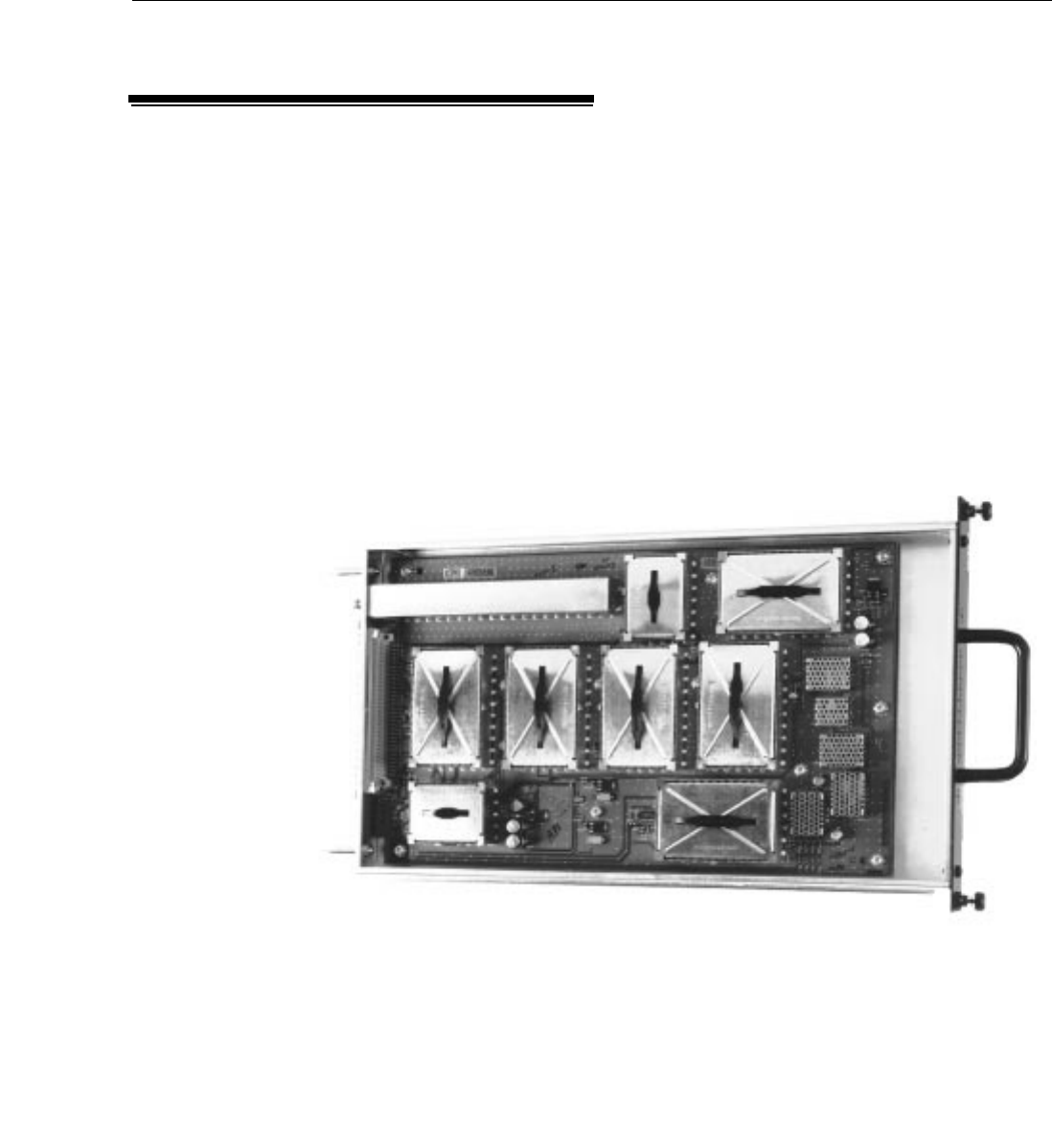
68P81095E02-D 4/1/2000
7-47
EBTS System Manual - Vol 2 800/900/1500 MHz Base Radio
1500 MHz Receiver – TLN3427
1500 MHz Receiver – TLN3427
Overview
The Receiver module provides the receiver functions for the Repeater. It consists
of a receiver board, a slide-in module housing, and associated hardware.
The receiver module assembly interconnects with the backplane through a 96-pin
connector and a blindmate RF connector. Two captive panel fasteners located on
the front of the module hold it in the chassis.
Figure 7-2 shows a top view of the Receiver module with the module cover
removed.
Theory of Operation
The Receiver module performs highly selective bandpass Þltering and dual
down-conversion of the station receive RF signal. A custom receiver IC outputs
the baseband information in a differential data format and sends it to the Base
Radio Controller module (BRC).
Table 7-8 lists and describes the Receiver circuitry and Figure 7-5 shows the
functional block diagram.
1.5GHZ-B853
Figure:7-2
Receiver (with top removed)

7-48
68P81095E02-D 4/1/2000
800/900/1500 MHz Base Radio EBTS System Manual - Vol 2
1500 MHz Receiver – TLN3427
Frequency Synthesizer and VCO Circuitry
The synthesizer and VCO circuitry generate the RF signal used to produce the 1st
LO injection signal for the 1st mixer in the receiver front end circuitry. Functional
operation of these circuits involves a Phase-Locked Loop (PLL) and VCO.
Phase-Locked Loop
The PLL IC receives frequency selection data from the BRC module
microprocessor via the SPI bus. Once programmed, the PLL IC compares a 2.1
MHz reference signal from the BRC with a feedback sample of the VCO output
from its feedback buffer.
Correction pulses are generated by the PLL IC, depending on whether the
feedback signal is higher or lower in frequency than the 2.1 MHz reference. The
width of these pulses is dependent on the amount of difference between the 2.1
MHz reference and the VCO feedback.
The up/down pulses are fed to a charge pump circuit that outputs a dc voltage
proportional to the pulse widths. This dc voltage is low-pass Þltered and fed to
the VCO circuit as the control voltage. The control voltage is between +2.5 Vdc
and +7.5 Vdc.
VCO
The dc control voltage from the synthesizer is fed to the VCO, which generates
the RF signal used to produce the 1st LO injection signal. The VCO responds to
the dc control voltage by generating the appropriate RF signal. A sample of this
signal is returned to the PLL IC through a buffer to close the VCO feedback loop.
Most of this signal is fed through a buffer to the doubler .
Table 7-8
Receiver Circuitry and Functions
Receiver Circuit This Circuit . . .
Frequency
Synthesizer
Circuitry
consists of a phase-locked loop and VCO. It generates the 1st LO
injection signal.
Receiver Front-End
Circuitry
provides Þltering, ampliÞcation, and the 1st down-conversion of
the receive RF signal. Digital step attenuators at the 1st IF are
included in this block.
Custom Receiver IC
Circuitry
consists of a custom IC to perform the 2nd down-conversion,
Þltering, ampliÞcation, and conversion of the receive signal. This
block outputs the receive signal as differential data to the BRC
module.
Address Decode,
A/D Converter, &
Memory Circuitry
performs address decoding for board and chip select signal,
converts analog status signals to digital format for use by the
BRC module. A memory device holds module speciÞc
information.
Local Power Supply
Regulation
accepts +14.2 Vdc input from the backplane interconnect board
and generates two +10 Vdc signals and two +5 Vdc signals for
the receiver module.

68P81095E02-D 4/1/2000
7-49
EBTS System Manual - Vol 2 800/900/1500 MHz Base Radio
1500 MHz Receiver – TLN3427
The frequency doubler is used to double the frequency of the RF signal from the
VCO to produce the 1st LO injection signal. This frequency-doubled signal is sent
to the injection ampliÞer to provide the 1st LO injection signal to the mixer in the
receiver front end circuitry.
Receiver Front End Circuitry
The station receive RF signal enters the receiver module through the RF-type
connector located on the receiver board. This signal is low-pass Þltered. It is then
sent to the preselector, and ampliÞed. The ampliÞed output is image Þltered
before being input to the 1st mixer. The signal mixes with the 1st LO injection
signal to produce a 73.35 MHz 1st IF signal.
The 1st IF signal is sent through a 4-pole bandpass Þlter and fed to a buffer
ampliÞer. The signal is 4-pole bandpass Þltered again. The resultant signal passes
through a digital attenuator. This attenuation is determined by the BRC module.
The signal is then fed to the RF input of the custom receive IC.
Custom Receiver IC Circuitry
The custom receiver IC provides additional ampliÞcation, Þltering, and a second
down-conversion. The 2nd IF signal is converted to a digital signal and is output
via differential driver circuitry to the BRC. This data signal contains the necessary
I and Q information, AGC information, and other data transfer information
required by the BRC to process the receive signal.
The remainder of the custom receiver IC circuitry consists of timing and tank
circuits to support the internal oscillator, 2nd LO synthesizer circuitry, and 2nd IF
circuitry.
A serial bus provides data communications between the custom receiver IC and
the DSP Glue ASIC (DGA) located on the BRC. This bus enables the DGA to
control various current and gain settings, establish the data bus clock rate,
program the 2nd LO, and perform other control functions.
Address Decode, Memory, and A/D Converter Circuitry
The Address Decode, Memory and A/D Converter circuitry performs address
decoding for board and chip select signals, converts analog status signals to
digital format, and the memory holds module speciÞc information.
Address Decode Circuitry
The address decode circuitry enables the BRC module to use the address bus. The
BRC can select a speciÞc device on a speciÞc station module via the SPI bus for
control or data communication purposes.
If the board select circuitry decodes address lines A2 through A5 as the receiver
module address, it enables the chip select circuitry. The chip select circuitry then
decodes address lines A0 and A1 to generate the chip select signals for the
EEPROM, A/D converter, and PLL IC.

7-50
68P81095E02-D 4/1/2000
800/900/1500 MHz Base Radio EBTS System Manual - Vol 2
1500 MHz Receiver – TLN3427
Memory Circuitry
The memory circuitry consists of an EEPROM located on the receiver module.
The BRC module performs all memory read and write operations via the SPI bus.
Information stored in this memory device includes the kit number, revision
number, module speciÞc scaling and correction factors, and free form module
information (scratch pad).
A/D Converter Circuitry
Analog signals from various strategic operating points throughout the receiver
board are fed to the A/D converter. These analog signals are converted to a digital
signal and are output to the BRC via the SPI lines upon request of the BRC
module.
Voltage Regulator Circuitry
The voltage regulator circuitry consists of two +10 Vdc and two +5 Vdc
regulators. The +10 Vdc regulators accept the +14.2 Vdc input from the backplane
interconnect board. Both regulators generate a +10 Vdc operating voltage for the
receiver board circuitry.
One of the +10 Vdc regulators feed two +5 Vdc regulators, which outputs an
Analog +5 Vdc and Digital +5 Vdc operating voltages for use by the custom
receiver IC.
A +5.1 Vdc operating voltage is also available from the backplane interconnect
board to supply +5.1 Vdc to the remainder of the receiver board circuitry.
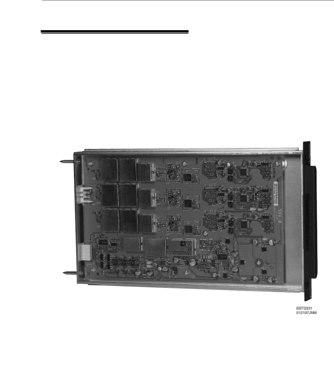
68P81095E02-D 4/1/2000
7-51
EBTS System Manual - Vol 2 800/900/1500 MHz Base Radio
800 MHz QUAD Channel Receiver – CLN1283;
800 MHz QUAD Channel Receiver – CLN1283;
Overview
The QUAD receiver provides receiver functions for the QUAD Channel Base
Radio. The QUAD receiver consists of a receiver board, a slide-in housing, and
associated hardware. A a single module of the QUAD receiver incorporates one
to three diversity branches. Figure 7-3 shows a top view of the Receiver with the
cover removed.
Diversity Uses and Cautions
The 3X receiver board can be used in one, two, or three-branch diversity systems.
The
rx_fru_config
parameter determines the number of active receivers. To
view the
rx_fru_config
parameter, use the MMI command.
(See software
commands.)
Each repeaterÕs conÞguration can be changed in the Þeld to match
the number of receivers connected to antennas. To change the rx_fru_conÞg
Figure:7-3
3X Receiver (with cover removed)
T
HIS
P
ICTURE
MUST
BE
CHANGED
!

7-52 68P81095E02-D 4/1/2000
800/900/1500 MHz Base Radio EBTS System Manual - Vol 2
800 MHz QUAD Channel Receiver – CLN1283;
parameter, use the command (reference software commands). In this command,
yyy is the active receiver. (Note: yyy is 1 for one branch, 12 for two branch, and
123 for three branch diversity.) For the iDEN system to work optimally, the
rx_fru_config parameter must match the number of receivers connected to
antennas.
CAUTION
Improperly setting the rx_fru_config parameter will
cause serious system degradation.
Modifying Base Radios from Three Branch to Two
Branch Diversity
When modifying a three-branch Base Radio to a two-branch Base Radio,
observing all precautionary statements in the previous paragraph is important.
To modify a three-branch Base Radio to a two-branch Base Radio:
1. Disconnect the RF cable from the RX3 connector on the Base Radio.
2. Connect an SMA male load (Motorola part number 5882106P03) to the RX3
connector on the Base Radio.
The SMA male load is required to limit the amount of radiated emissions.
3. Verify that the rx_fru_config parameter is set properly, according to the
Diversity Uses and Caution paragraph above.

68P81095E02-D 4/1/2000 7-53
EBTS System Manual - Vol 2 800/900/1500 MHz Base Radio
800 MHz QUAD Channel Receiver – CLN1283;
Modifying Base Radios from Two Branch to Three
Branch Diversity
1. Remove the SMA male load from the RX3 connector of the Base Radio that
you wish to convert from two-branch diversity to three-branch diversity.
2. Connect the Receive Antenna #3 RF cable to the RX3 connector on the Base
Radio.
3. Verify that the rx_fru_config parameter is set properly, according to the
Diversity Uses and Cautions paragraph.
Theory of Operation
The Receiver performs highly selective bandpass Þltering and dual down
conversion of the station receive RF signal. A custom Receiver IC outputs the
baseband information in a differential data format and sends it to the BRC.
Table 7-7 lists the Receiver circuitry. Figure 7-6 shows a functional block diagram
for the Receiver.
Frequency Synthesizer and VCO Circuitry
The synthesizer and VCO circuitry generate the RF signal used to produce the
1st LO injection signal for the Þrst mixer in all the Receiver front end circuits.
Functional operation of these circuits involves a Phase-Locked Loop (PLL) and
VCO.
The PLL IC receives frequency selection data from the BRC module
microprocessor via the SPI bus. Once programmed, the PLL IC compares a
2.1 MHz reference signal from the BRC with a feedback sample of the VCO
output from its feedback buffer.
Table 7-9
Receiver Circuitry
Circuit Description
Frequency
Synthesizer Circuitry
Consists of a phase-locked loop and VCO. It generates the 1st LO
injection signal for all three receivers.
Receiver Front-End
Circuitry
Provides Þltering, ampliÞcation, and the 1st down conversion of the
receive RF signal. This block includes digital step attenuators at the 1st
IF.
Custom Receiver IC
Circuitry
Consists of a custom IC to perform the 2nd down conversion, Þltering,
ampliÞcation, and conversion of the receive signal. This block outputs
the receive signal as differential data to the BRC.
Address Decode,
A/D Converter, &
Memory Circuitry
Performs address decoding for board and chip-select signals. Converts
analog status signals to digital format for use by the BRC. A memory
device holds module-speciÞc information.
Local Power Supply
Regulation
Accepts +14.2 Vdc input from the backplane interconnect board. Also
generates two +10 Vdc, a +11.5 Vdc, and two +5 Vdc signals for the
receiver.

7-54 68P81095E02-D 4/1/2000
800/900/1500 MHz Base Radio EBTS System Manual - Vol 2
800 MHz QUAD Channel Receiver – CLN1283;
The PLL ICC generates correction pulses, depending on whether the feedback
signal is higher or lower in frequency than the 2.1 MHz reference. The width of
these pulses depends on the amount of difference between the 2.1 MHz reference
and the VCO feedback.
The up/down pulses enter a charge pump circuit. The charge pump outputs a DC
voltage proportional to the pulse widths. After low-pass Þltering, this DC voltage
enters the VCO circuit as the control voltage. The control voltage measures
between +2.5 Vdc and +7.5 Vdc.
The DC control voltage from the synthesizer is enters the VCO. The VCO
generates the RF signal that the circuit uses to produce the 1st LO injection signal.
The VCO responds to the DC control voltage by generating the appropriate RF
signal. This signal passes through a buffer to the 1st LO injection ampliÞer. A
sample of this signal returns to the PLL IC through a buffer to close the VCO
feedback loop.
Receiver Front End Circuitry
The station receive RF signal enters the Receiver through the RF-type connector
on the back of the Receiver board. The circuit low-pass Þlters and ampliÞes this
signal. The ampliÞed output passes through an image Þlters before entering the
1st mixer. The signal mixes with the 1st LO injection signal to produce a 73.35
MHz 1st IF signal.
The 1st IF signal passes through a four-pole, bandpass Þlter and enters a buffer
ampliÞer. The buffer ampliÞer output signal again undergoes four-pole,
bandpass Þltering. The resultant signal then passes through a digital attenuator.
The BRC determines the amount of attenuation. The resulting signal then enters
the RF input of the custom Receiver IC.
Custom Receiver IC Circuitry
The custom Receiver IC provides additional ampliÞcation, Þltering, and a second
down-conversion. The IC converts the 2nd IF signal to a digital signal. The digital
signal exits the receiver IC via differential driver circuitry, and passes to the BRC.
This data signal contains I and Q information, AGC information, and other data
transfer information. The BRC uses this information to facilitate processing of the
receive signal.
The remainder of the custom Receiver IC circuitry consists of timing and tank
circuits. These circuits support the internal oscillator, 2nd LO synthesizer, and 2nd
IF circuitry.
A serial bus provides data communications between the custom Receiver IC and
the DSP Glue ASIC (DGA). These circuits are on the BRC. The serial bus enables
the DGA to perform several control functions...
❐control various current and gain settings
❐establish the data bus clock rate
❐program the 2nd LO
❐perform other control functions

68P81095E02-D 4/1/2000 7-55
EBTS System Manual - Vol 2 800/900/1500 MHz Base Radio
800 MHz QUAD Channel Receiver – CLN1283;
Address Decode Circuitry
Address decode circuitry enables the BRC to use the SPI bus to select a speciÞc
device on a speciÞc Receiver for control or data communication purposes.
If board-select circuitry decodes address lines A2 through A5 as the Receiver
address, it enables the chip select circuitry. The chip select circuitry then decodes
address lines A0 and A1. The decoding process generates the chip select signals
for the EEPROM, A/D converter, and PLL IC.
Memory Circuitry
The memory circuitry consists of three EEPROMs located on the Receiver. The
BRC performs memory read and write operations via the SPI bus. Information
stored in this memory device includes...
❐the kit number
❐revision number
❐module speciÞc scaling and correction factors
❐free form module information (scratch pad)
A/D Converter Circuitry
Analog signals from various strategic operating points throughout the Receiver
board pass through the A/D converter. These analog signals become a digital
signal. Upon request of the BRC, this signal travels to the BRC via the SPI lines.
Voltage Regulator Circuitry
The voltage regulator circuitry consists of two +10 Vdc, a +10.8 Vdc, and two
+5 Vdc regulators. The two +10 Vdc and the +10.8 Vdc regulators accept the
+14.2 Vdc input from the backplane interconnect board. These regulators produce
operating voltages for the Receiver circuitry.
The +10 Vdc regulators each feed a +5 Vdc regulator. One of these regulators
outputs Analog +5 Vdc. The other regulator outputs Digital +5 Vdc operating
voltages for use by the custom Receiver IC.
The backplane interconnect board also produces a +5.1 Vdc operating voltage.
This voltage powers the remainder of the Receiver circuitry.

7-56 68P81095E02-D 4/1/2000
800/900/1500 MHz Base Radio EBTS System Manual - Vol 2
This Page Intentionally
Left Blank

68P81095E02-D 4/1/2000
7-57
EBTS System Manual - Vol 2 800/900/1500 MHz Base Radios
Receiver
7
RECEIVER #3 FRONT END CIRCUITRY
RECEIVER #2 FRONT END CIRCUITRY
RECEIVE RF
FROM RX ANTENNA
(MULTICOUPLER)
SMA-TYPE
CONNECTOR
2.1 MHZ REF
FROM CONTROL
MODULE
SPI BUS
TO/FROM CONTROL
MODULE
ADDRESS BUS
FROM CONTROL
MODULE
DIFFERENTIAL
DATA
TO CONTROL
MODULE
SERIAL BUS
TO/FROM CONTROL
MODULE
ADDRESS DECODE, MEMORY, & A/D
CONVERTER CIRCUITRY
CHIP SELECT
DECODE CIRCUITRY
RECEIVER SELECT
DECODE CIRCUITRY
MEMORY #1
SYNTHESIZER
CIRCUITRY
CHARGE
PUMP
PHASE
LOCKED
LOOP
IC
+10 V
REGULATOR
REGULATORY
CIRCUITRY
VCO
CIRCUITRY
+10 V
AGC
FROM CONTROL
MODULE
LO-PASS
FILTER HI-PASS
FILTER PREAMPLIFIER
CIRCUITRY
RECEIVER #1 FRONT END CIRCUITRY
2ND LO
VCO
14.4 MHZ
TIMING
CIRCUITRY
450 KHZ
FILTER
CIRCUITRY
DRIVER
CIRCUITRY
CUSTOM RECEIVER
IC CIRCUITRY
(ABACUS #1 )
DIGITAL
ATTENUATOR
CIRCUITRY
73.35 MHZ
1ST IF
CUSTOM
RECEIVER
IC
VCO
FEEDBACK
BUFFER
BUFFER
SUPER
FILTER
OSCILLATOR
BUFFER
AMP
LO-PASS
LOOP
FILTER
CONTROL
VOLTAGE
(+2.5 TO +7.5 VDC)
VCO FEEDBACK
2.1 MHZ REFERENCE
CHIP
SELECT
CHIP
SELECT
SECOND
+10 V
SOURCE
+14.2 V
FROM
BACKPLANE
+10 V
REGULATOR
+5 V
REGULATOR
+5 V
REGULATOR
DIGITAL
+5 V
SOURCE
+10 V
SOURCE
ANALOG
+5 V
SOURCE
CHIP
SELECT
FIN
RIN
VCO
FEEDBACK
SPI BUS (CLOCK & DATA)
VARIOUS
SIGNALS
TO MONITOR
2.1 MHZ REF
4-POLE
BANDPASS
FILTER
4-POLE
BANDPASS
FILTER
1ST
MIXER
EBTS293
120597JNM
VCO
MEMORY #2
MEMORY #3
#3 A/D
CONVERTER
#2 A/D
CONVERTER
#1 A/D
CONVERTER
+10 V
REGULATOR
INJECTION
AMPLIFIER
TO RECEIVER #2 MIXER
TO RECEIVER #3 MIXER
ABACUS #2
ABACUS #3
3 WAY
SPLITTER
(NOTE)
NOTE: 14.4 MHz TIMING CIRCUITRY AND 2ND LO VCO PRESENT ONLY ON ABACUS #2.
FUNCTIONS ARE SHARED FOR ALL THREE ABACUS SECTIONS.
Figure:7-4
3X Receiver Functional Block Diagram
3X Receiver
Functional Block Diagram
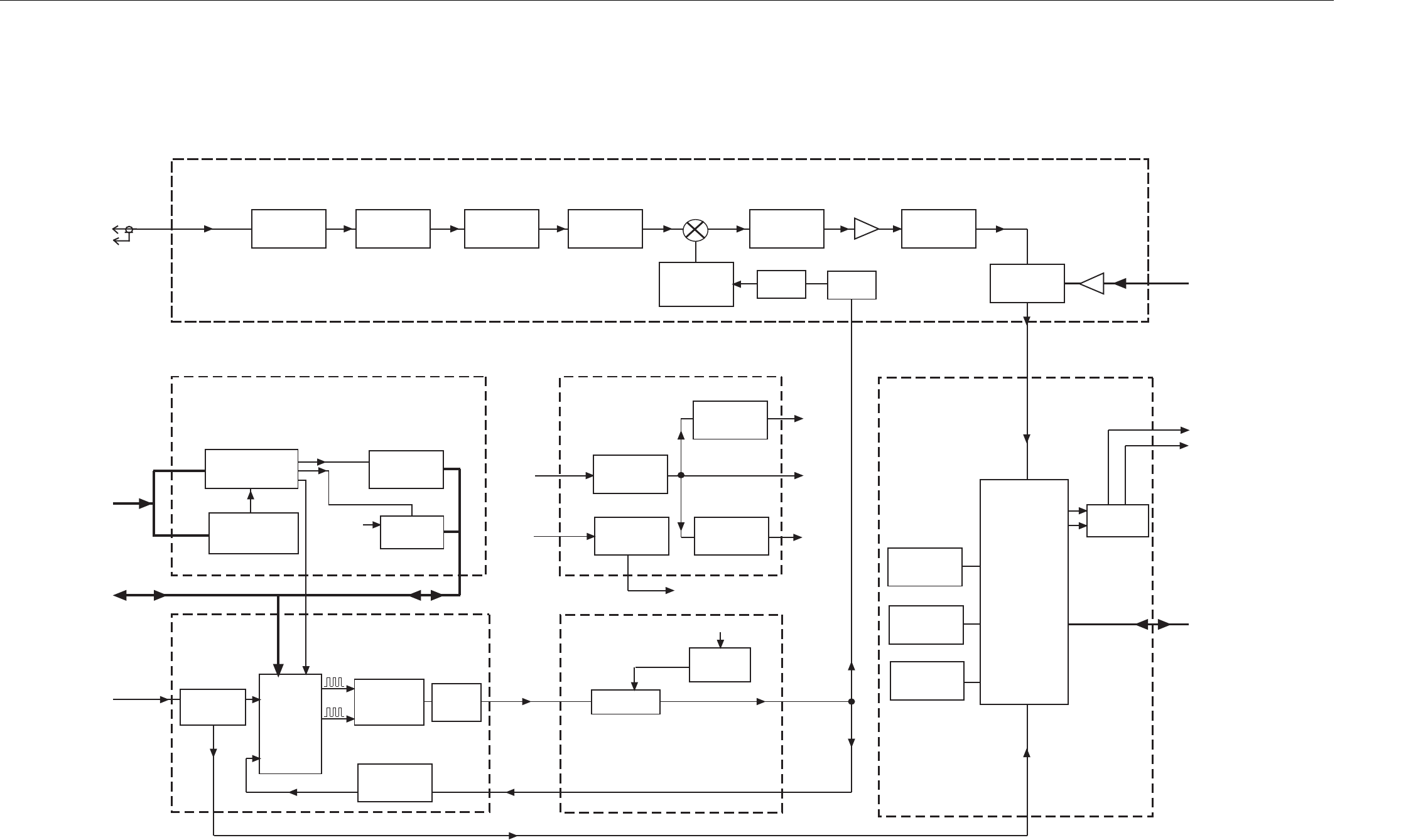
7-58
68P81095E02-D 4/1/2000
800/900/1500 MHz Base Radios EBTS System Manual - Vol 2
Receiver
7
Receiver
Functional Block Diagram
Model TLN3427
RECEIVE RF
FROM RX ANTENNA
(MULTICOUPLER)
2.1 MHZ REF
FROM BRC
MODULE
SPI BUS
TO/FROM BRC
MODULE
ADDRESS BUS
FROM BRC
MODULE
DIFFERENTIAL
DATA (DSP BUS)
TO BRC
MODULE
SERIAL BUS
TO/FROM BRC
MODULE
ADDRESS DECODE, MEMORY, & A/D
CONVERTER CIRCUITRY
CHIP SELECT
DECODE CIRCUITRY
(U2804)
BOARD SELECT
DECODE CIRCUITRY
(U2804)
EEPROM
MEMORY
(U2601)
SYNTHESIZER
CIRCUITRY
PHASE
LOCKED
LOOP IC
(U2401)
+10 V
REGULATOR
(U2702)
REGULATORY
CIRCUITRY
VCO
CIRCUITRY
+10 V
AGC
FROM BRC
MODULE
LOW-PASS
FILTER
(L2000, C2000,
C2001, C2002)
PRESELECTOR
FILTER
(FL2000)
PREAMPLIFIER
CIRCUITRY
(Q2030, Q2031)
IMAGE
FILTER
CIRCUITRY
(FL2070)
RECEIVER FRONT END CIRCUITRY
2ND LO
TANK
CIRCUITRY
14.4 MHZ
TIMING
CIRCUITRY
450 KHZ
FILTER
CIRCUITRY
DRIVER
CIRCUITRY
(U2501)
CUSTOM
RECEIVER IC
CIRCUITRY
DIGITAL
ATTENUATOR
CIRCUITRY
(U2100)
73.35 MHZ
1ST IF
CUSTOM
RECEIVER IC
(U2500)
VCO
FEEDBACK
BUFFER
(Q2401)
SUPER
FILTER
(Q2280)
OSCILLATOR
(U2200)
LOW-PASS
LOOP
FILTER
(U2403)
CONTROL
VOLTAGE
(+2.5 TO +7.5 VDC)
VCO FEEDBACK
2.1 MHZ REFERENCE
1ST LO
INJ AMP
CIRCUITRY
(Q2302, Q2303,
FL2300)
CHIP SELECT
SECOND
+10 V
SOURCE
+14.2 V
FROM
BACKPLANE
+10 V
REGULATOR
(U2703)
+5 V
REGULATOR
(U2700)
+5 V
REGULATOR
(U2701)
DIGITAL
+5 V
SOURCE
+10 V
SOURCE
ANALOG
+5 V
SOURCE
CHIP
SELECT
FIN
RIN
VCO
FEEDBACK
SPI BUS (CLOCK & DATA)
VARIOUS
SIGNALS
TO MONITOR
A/D
CONVERTER
(U2600)
2.1 MHZ REF
4-POLE
BANDPASS
FILTER
(Y2100)
4-POLE
BANDPASS
FILTER
(Y2101)
1ST
MIXER
(CR2070)
BUFFER
AMP
(Q2100)
LINE
DRIVER
(U2805)
DOUBLER
(Q2301)
REFERENCE
BUFFER
(Q2402)
CHARGE PUMP
(Q2405, Q2406,
Q2407, Q2408,
Q2409)
CHIP SELECT
BUFFER
AMP
(Q2300)
Figure:7-5
1500 MHz Receiver Functional Block Diagram
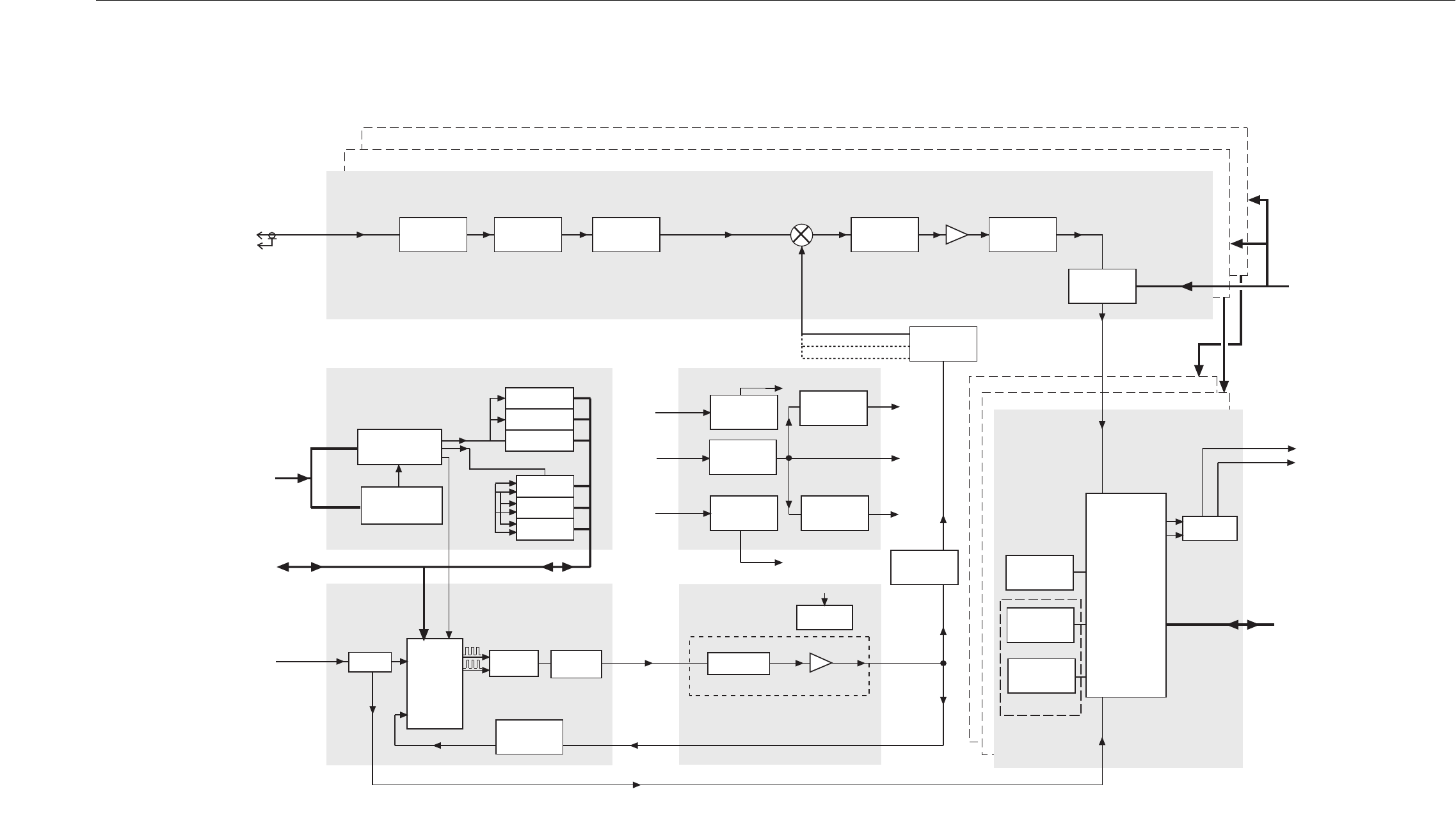
68P81095E02-D 4/1/2000
7-59
EBTS System Manual - Vol 2 800/900/1500 MHz Base Radios
Receiver
7
RECEIVER #3 FRONT END CIRCUITRY
RECEIVER #2 FRONT END CIRCUITRY
RECEIVE RF
FROM RX ANTENNA
(MULTICOUPLER)
SMA-TYPE
CONNECTOR
2.1 MHZ REF
FROM CONTROL
MODULE
SPI BUS
TO/FROM CONTROL
MODULE
ADDRESS BUS
FROM CONTROL
MODULE
DIFFERENTIAL
DATA
TO CONTROL
MODULE
SERIAL BUS
TO/FROM CONTROL
MODULE
ADDRESS DECODE, MEMORY, & A/D
CONVERTER CIRCUITRY
CHIP SELECT
DECODE CIRCUITRY
RECEIVER SELECT
DECODE CIRCUITRY
MEMORY #1
SYNTHESIZER
CIRCUITRY
CHARGE
PUMP
PHASE
LOCKED
LOOP
IC
+10 V
REGULATOR
REGULATORY
CIRCUITRY
VCO
CIRCUITRY
+10 V
AGC
FROM CONTROL
MODULE
LO-PASS
FILTER HI-PASS
FILTER PREAMPLIFIER
CIRCUITRY
RECEIVER #1 FRONT END CIRCUITRY
2ND LO
VCO
14.4 MHZ
TIMING
CIRCUITRY
450 KHZ
FILTER
CIRCUITRY
DRIVER
CIRCUITRY
CUSTOM RECEIVER
IC CIRCUITRY
(ABACUS #1 )
DIGITAL
ATTENUATOR
CIRCUITRY
73.35 MHZ
1ST IF
CUSTOM
RECEIVER
IC
VCO
FEEDBACK
BUFFER
BUFFER
SUPER
FILTER
OSCILLATOR
BUFFER
AMP
LO-PASS
LOOP
FILTER
CONTROL
VOLTAGE
(+2.5 TO +7.5 VDC)
VCO FEEDBACK
2.1 MHZ REFERENCE
CHIP
SELECT
CHIP
SELECT
SECOND
+10 V
SOURCE
+14.2 V
FROM
BACKPLANE
+10 V
REGULATOR
+5 V
REGULATOR
+5 V
REGULATOR
DIGITAL
+5 V
SOURCE
+10 V
SOURCE
ANALOG
+5 V
SOURCE
CHIP
SELECT
FIN
RIN
VCO
FEEDBACK
SPI BUS (CLOCK & DATA)
VARIOUS
SIGNALS
TO MONITOR
2.1 MHZ REF
4-POLE
BANDPASS
FILTER
4-POLE
BANDPASS
FILTER
1ST
MIXER
EBTS293
120597JNM
VCO
MEMORY #2
MEMORY #3
#3 A/D
CONVERTER
#2 A/D
CONVERTER
#1 A/D
CONVERTER
+10 V
REGULATOR
INJECTION
AMPLIFIER
TO RECEIVER #2 MIXER
TO RECEIVER #3 MIXER
ABACUS #2
ABACUS #3
3 WAY
SPLITTER
(NOTE)
NOTE: 14.4 MHz TIMING CIRCUITRY AND 2ND LO VCO PRESENT ONLY ON ABACUS #2.
FUNCTIONS ARE SHARED FOR ALL THREE ABACUS SECTIONS.
Figure:7-6
3X Receiver Functional Block Diagram
QUAD Receiver
Functional Block Diagram
T
HIS
P
ICTURE
MUST
BE
CHANGED
!

7-60
68P81095E02-D 4/1/2000
800/900/1500 MHz Base Radios EBTS System Manual - Vol 2
Receiver
This Page Intentionally
Left Blank

68P81095E02-D 4/1/2000
8-1
EBTS System Manual - Vol 2 800/900/1500 MHz Base Radios
8 Troubleshooting
Single Channel Base
Radios
Overview
This chapter isolates single channel Base Radio failures to the FRU level. The
chapter contains procedures for:
chapter contains procedures for:
❐
Troubleshooting
❐
VeriÞcation
❐
Station Operation
The Base Radio maintenance philosophy is repair by replacing defective FRUs
with new FRUs. This maintenance method limits down-time, and quickly
restores the Base Radio to normal operation.
Two Base Radio troubleshooting procedures appear here. Each procedure quickly
identifies faulty FRUs.
Ship defective FRUs to a Motorola repair depot for repair.
Recommended Test Equipment
Table 8-1 lists recommended test equipment for performing Base Radio
troubleshooting and veriÞcation procedures.

8-2
68P81095E02-D 4/1/2000
800/900/1500 MHz Base Radios EBTS System Manual - Vol 2
Table 8-1
Recommended Test Equipment
Test Equipment Model Number Use
Communications Analyzer R2660 w/iDEN option Used for checking receive and
transmit operation (iDEN
signaling capability) and station
alignment
Dummy Load (50
Ω
, 150 W
)
none Used to terminate output
Service Computer IBM or clone, 80286 or
better
Local service terminal
Portable Rubidium
Frequency Standard
Ball Efratom Frequency standard for R2660,
netting TFR
Power Meter none Used to measure reßected and
forward power
RF Attenuator, 250 W, 10 dB Motorola 0180301E72 Protection for R2660
Software:
Communication
File Compression
Procomm Plus
PKZip
Local service computer
Compress/Decompress data

68P81095E02-D 4/1/2000
8-3
EBTS System Manual - Vol 2 800/900/1500 MHz Base Radios
Troubleshooting Procedures
Many of the troubleshooting and station operation procedures require
Man-Machine Interface (MMI) commands. These commands are used to
communicate station level commands to the Base Radio via the RS-232
communications port located on the front of the BRC.
Routine Checkout
Procedure 1 is a quick, non-intrusive test performed during a routine site visit.
Use this procedure to verify proper station operation without taking the station
out of service. Figure 8-1 shows the Procedure 1 Troubleshooting Flowchart.
Figure:8-1
Procedure 1 Troubleshooting Flowchart
PROCEDURE 1
ROUTINE
SITE VISIT
OBSERVE LED
INDICATORS
Module Suspected
of Being Faulty?
No
No
DONE
CHECK CURRENT
ALARM STATUS
Use MMI command
get alarms
to check alarm status
Module Suspected
of Being Faulty?
Ye s Go to Troubleshooting
Procedure 2 Flow Chart
Ye s Go to Troubleshooting
Procedure 2 Flow Chart
Refer to
Controls and Indicators
for LED Definitions
EBTS021
071895JNM

8-4
68P81095E02-D 4/1/2000
800/900/1500 MHz Base Radios EBTS System Manual - Vol 2
Reported/Suspected Problem
Use Procedure 2 to troubleshoot reported or suspected equipment malfunctions.
Perform this procedure with equipment in service (non-intrusive) and with
equipment taken temporarily out of service (intrusive).
Figure 8-2 shows the Procedure 2 Troubleshooting Flowchart.
Figure:8-2
Procedure 2 Troubleshooting Flowchart
PROCEDURE 2
PROBLEM
REPORTED OR SUSPECTED
DONE
Clear Problem Report
OBSERVE LED
INDICATORS
Module Suspected
of Being Faulty?
Ye s Go to Module Replacement
Procedures Section
No
CHECK CURRENT
ALARM STATUS
Use MMI command
get alarms
to check alarm status
Module Suspected
of Being Faulty? Go to Module Replacement
Procedures Section
PERFORM
VERIFICATION TESTS
Use MMI commands to
perform tests as specified in
station verification procedure.
Module Suspected
of Being Faulty? Go to Module Replacement
Procedures Section
Ye s
No
Ye s
No
Refer to
Controls and Indicators
for LED Definitions
EBTS022
071895JNM

68P81095E02-D 4/1/2000
8-5
EBTS System Manual - Vol 2 800/900/1500 MHz Base Radios
Base Radio/Base Radio FRU Replacement Procedures
Base Radio/Base Radio FRU
Replacement Procedures
Replace suspected station modules with known non-defective modules to restore
the station to proper operation. The following procedures provide FRU
replacement instructions and post-replacement adjustments and/or
veriÞcation instructions.
Base Radio Replacement Procedure
NOTE
The Base Radio removal and installation procedures
are included for reference or buildout purposes. Field
maintenance of Base Radios typically consists of
replacement of FRUs within the Base Radio. Perform
Base Radio FRU replacement in accordance with ÒBase
Radio FRU Replacement ProcedureÓ below.
Perform Base Radio (BR) replacement as described in the following paragraphs.
Removal
Remove BR from Equipment Cabinet as follows:
1.
Remove power from the Base Radio by setting the Power Supply ON/OFF
switch to the OFF position.
2.
Tag and disconnect the cabling from the BR rear panel connectors.
3.
Remove the four M6 TORX screws which secure the BR front panel to the
Equipment Cabinet mounting rails.
WARNING
!
BR WEIGHT EXCEEDS 60 LBS (27 KG). USE
TWO-PERSON LIFT WHEN REMOVING OR INSTALLING
BR FROM EQUIPMENT CABINET. MAKE CERTAIN BR IS
FULLY SUPPORTED WHEN BR IS FREE FROM
MOUNTING RAILS.
4.
While supporting the BR, carefully remove the BR from the Equipment
Cabinet by sliding the BR from the front of cabinet.

8-6
68P81095E02-D 4/1/2000
800/900/1500 MHz Base Radios EBTS System Manual - Vol 2
Base Radio/Base Radio FRU Replacement Procedures
Installation
Install BR in Equipment Cabinet as follows:
1.
If adding a BR, install side rails in the appropriate BR mounting position in
the rack.
2.
While supporting the BR, carefully lift and slide the BR in the Equipment
Cabinet mounting position.
3.
Secure the BR to the Equipment Cabinet mounting rails using four M6
TORX screws. Tighten the screws to 40 in-lb (4.5 Nm).
4.
Connect the cabling to the BR rear panel connectors as tagged during the BR
removal. If adding a BR, perform the required cabling in accordance with
the Cabling Information subsection of the RFDS section applicable to the
system.
5.
Perform BR activation in accordance with Station VeriÞcation Procedures
below.
Anti-Static Precautions
CAUTION
The Base Radio contains static-sensitive devices.
when replacing Base Radio FRUs, always wear a
grounded wrist strap and observe proper anti-static
procedures to prevent electrostatic discharge damage
to Base Radio modules.
Motorola publication 68P81106E84 provides complete static protection
information. This publication is available through Motorola National Parts.
Observe the following additional precautions:
❐
Wear a wrist strap (Motorola Part No. 4280385A59 or equivalent) at all times
when servicing the Base Radio to minimize static build-up.
❐
A grounding clip is provided with each EBTS cabinet. If not available, use
another appropriate grounding point.
❐
DO NOT insert or remove modules with power applied to the Base Radio.
ALWAYS turn the power OFF using the Power Supply rocker switch on the
front of the Power Supply module.
❐
Keep spare modules in factory packaging for transporting. When shipping
modules, always pack in original packaging.
FRU Replacement Procedure
Perform the following steps to replace any of the Base Radio FRUs:

68P81095E02-D 4/1/2000
8-7
EBTS System Manual - Vol 2 800/900/1500 MHz Base Radios
Base Radio/Base Radio FRU Replacement Procedures
NOTE
When servicing Base Radios (BRs), in situations where
the Control Board or the entire BR is replaced, the
integrated Site Controller (iSC) will automatically
reboot the serviced BR given that the BR has been
off-line for a period not less than that stipulated by the
ÒReplacement BRC Accept TimerÓ (default is 3
minutes). If the BR is turned on prior to the expiration
of the ÒReplacement BRC Accept TimerÓ, power the
BR back down and wait the minimum timer length
before turning the BR back on.
1.
Remove power from the Base Radio by setting the Power Supply rocker
switch (located behind the front panel of the Power Supply) to the OFF (0)
position.
2.
Loosen the front panel fasteners. These are located on each side of the
module being replaced.
3.
Pull out the module.
4.
Insert the non-defective replacement module by aligning the module side
rails with the appropriate rail guides inside the Base Radio chassis.
5.
Gently push the replacement module completely into the Base Radio chassis
assembly using the module handle(s).
CAUTION
DO NOT slam or force the module into the chassis
assembly. This will damage the connectors
or backplane.
6.
Secure the replacement module by tightening the front panel fasteners to the
speciÞed torque of 5 in-lbs.
7.
Apply power to the Base Radio by setting the switch to the ON position.
8.
Perform the Station VeriÞcation Procedure provided below.

8-8
68P81095E02-D 4/1/2000
800/900/1500 MHz Base Radios EBTS System Manual - Vol 2
Base Radio/Base Radio FRU Replacement Procedures
Power Amplifier (PA) Fan FRU Replacement
Perform the following steps to replace the Power AmpliÞer (PA) fans.
1.
Remove the Power AmpliÞer from the Base Radio per FRU Replacement
Procedure.
2.
Disconnect fan power cable from PA housing.
3.
Remove front panel from fan assembly.
4.
Remove fan assembly from PA chassis.
NOTE
Reverse above procedure to install new fan kit.

68P81095E02-D 4/1/2000
8-9
EBTS System Manual - Vol 2 800/900/1500 MHz Base Radios
Station Verification Procedures
Station Verification Procedures
Perform the Station VeriÞcation Procedures whenever you replace a FRU. The
procedures verify transmit and receive operations. Each procedure also contains
the equipment set-up.
Replacement FRU Verification
All module speciÞc information is programmed in the factory prior to shipment.
Base Radio speciÞc information (e.g., receive and transmit frequencies) is
downloaded to the Base Radio from the network/site controller.
Replacement FRU alignment is not required for the Base Radio.
Base Repeater FRU Hardware Revision Verification
NOTE
The following procedure requires the Base Radio to be
out of service. Unless the Base Radio is currently out
of service, Motorola recommends performing this
procedure during off-peak hours. This minimizes or
eliminates disruption of service to system users.
1.
Connect one end of the RS-232 cable to the service computer.
2.
Connect the other end of the RS-232 cable to the STATUS port, located on the
front panel of the BRC.
3.
Using the Þeld password, login to the BR.

8-10
68P81095E02-D 4/1/2000
800/900/1500 MHz Base Radios EBTS System Manual - Vol 2
Station Verification Procedures
4.
Collect revision numbers from the station by typing the
following commands:
5.
If all modules return revision numbers of the format ÒRxx.xx.xxÓ, then all
revision numbers are present and no further action is required. Log out and
repeat steps 1 through 4 for each additional BR.
If revision numbers were returned as blank or not in the format ÒRxx.xx.xxÓ,
contact your local Motorola representative or Technical Support.
6.
When all BRs have been checked, log out.
Transmitter Verification
The transmitter veriÞcation procedure veriÞes the transmitter operation and the
integrity of the transmit path. This veriÞcation procedure is recommended after
replacing an Exciter, Power AmpliÞer, BRC, or Power Supply module.
NOTE
The following procedure requires the Base Radio to be
out of service. Unless the Base Radio is currently out
of service, Motorola recommends performing this
procedure during off-peak hours. This minimizes or
eliminates disruption of service to system users.
Equipment Setup
To set up the equipment, use the following procedure:
1.
Remove power from the Base Radio by setting the Power Supply rocker
switch (located behind the front panel of the Power Supply) to the OFF (0)
position.
2.
Connect one end of the RS-232 cable to the service computer.
BRC>dekey
BRC>test_mode
BRC>get brc_rev_no
BRC>get rx1_rev_no
BRC>get rx2_rev_no
BRC>get rx3_rev_no (if BR is 3 branch)
BRC>get pa_rev_no
BRC>get ex_rev_no
BRC>

68P81095E02-D 4/1/2000
8-11
EBTS System Manual - Vol 2 800/900/1500 MHz Base Radios
Station Verification Procedures
3.
Connect the other end of the RS-232 cable to the STATUS port located on the
front panel of the BRC.
4.
Disconnect the existing cable from the connector labeled PA OUT.
This connector is located on the backplane of the Base Radio.
5.
Connect a test cable to the PA OUT connector.
6.
Connect a 10 dB attenuator on the other end of the test cable.
7.
From the attenuator, connect a cable to the RF IN/OUT connector on the
R2660 Communications Analyzer.
8.
Remove power from the R2660 and connect the Rubidium Frequency
Standard 10MHZ OUTPUT to a 10 dB attenuator.
9.
Connect the other end of the 10 dB attenuator to the 10MHZ REFERENCE
OSCILLATOR IN/OUT connector on the R2660.
NOTE
Refer to the equipment manual provided with the
R2660 for further information regarding mode
conÞguration of the unit (Motorola Part
No. 68P80386B72).
10.
Set the R2660 to the EXT REF
mode.
11.
Apply power to the R2660.
12. Set the R2660 to the SPECTRUM ANALYZER mode with the center
frequency set to the transmit frequency of the Base Radio under test.
13. Perform the appropriate transmitter veriÞcation procedure below for the
particular Power AmpliÞer used in the Base Radio.
Transmitter Verification Procedure
(40W, 800 MHz Power Amplifier – TLF2020)
This procedure provides commands and responses to verify proper operation of
the transmit path for 800 MHz Base Radios using a 40 Watt Power AmpliÞer.

8-12 68P81095E02-D 4/1/2000
800/900/1500 MHz Base Radios EBTS System Manual - Vol 2
Station Verification Procedures
1. Apply power to the Base Radio by setting the switch to the 1 position.
The following message displays on the service computer during power-up.
2. Enter the proper password. After entering the correct password, the BRC>
prompt is displayed on the service computer.
The default password is motorola
NOTE
Motorola recommends that you change the default
password once proper operation of the equipment is
veriÞed.
3. At the BRC> prompt, type: dekey
This command veriÞes that there is no RF power being transmitted.
CAUTION
The following command keys the transmitter. Make
sure that transmission only occurs on licensed
frequencies or into a RF load.
Base Radio
firmware revision RXX.XX.XX
Copyright 1998
Motorola, Inc. All rights reserved.
Unauthorized access prohibited
Enter login password:
BRC> dekey
XMIT OFF INITIATED

68P81095E02-D 4/1/2000 8-13
EBTS System Manual - Vol 2 800/900/1500 MHz Base Radios
Station Verification Procedures
4. At the BRC> prompt, type: set tx_power 40
This command sets the transmitter output to 40 Watts.
After keying the Base Radio, verify the forward and reßected powers of the
station along with the station VSWR with the parameters listed in Table 8-2.
5. At the BRC> prompt, type: get fwd_pwr
This command returns the current value of forward power from the RF
Power AmpliÞer.
Table 8-2
40W, 800 MHz PA Transmitter Parameters
Parameter Value or Range
Forward Power Greater than 38.0 Watts
Reßected Power Less than 4.0 Watts
VSWR Less than 2:1
BRC> set tx_power 40
setting transmitter power to 40 watts
TXLIN ATTENUATION: 5.000000
TARGET POWER: 40.00 watts [46.02 dBm]
ACTUAL POWER: 37.77 watts [45.07 dBm]
POWER WINDOW: 38.20-> 41.89 watts [45.82 -> 46.22 dBm]
TXLIN LEVEL REGISTER REDUCED 59 STEPS [-2.30 dB].
TXLIN LEVEL: 0x6f
completed successfully
BRC> get fwd_pwr
FORWARD POWER is 39.13 watts [45.92 dBm]

8-14 68P81095E02-D 4/1/2000
800/900/1500 MHz Base Radios EBTS System Manual - Vol 2
Station Verification Procedures
6. At the BRC> prompt, type: get ref_pwr
This command returns the current value of reßected power from the RF
Power AmpliÞer.
7. At the BRC> prompt, type: get vswr
This command calculates the current Voltage Standing Wave Ratio (VSWR)
from the RF Power AmpliÞer.
8. At the BRC> prompt, type: get alarms
This command returns all active alarms of the Base Radio.
NOTE
If the get alarms command displays alarms, refer to
the System Troubleshooting section of this manual for
corrective actions.
9. View the spectrum of the transmitted signal on the R2660 Communications
Analyzer in the Spectrum Analyzer mode. Figure 8-3 shows a sample of the
spectrum.
10. At the BRC> prompt, type: dekey
This command stops all transmitter activity.
BRC> get ref_pwr
REFLECTED POWER is 0.27 watts [24.28 dBm]
BRC> get vswr
VSWR is 1.17:1
BRC> get alarms
NO ALARM CONDITIONS DETECTED
BRC> dekey
XMIT OFF INITIATED
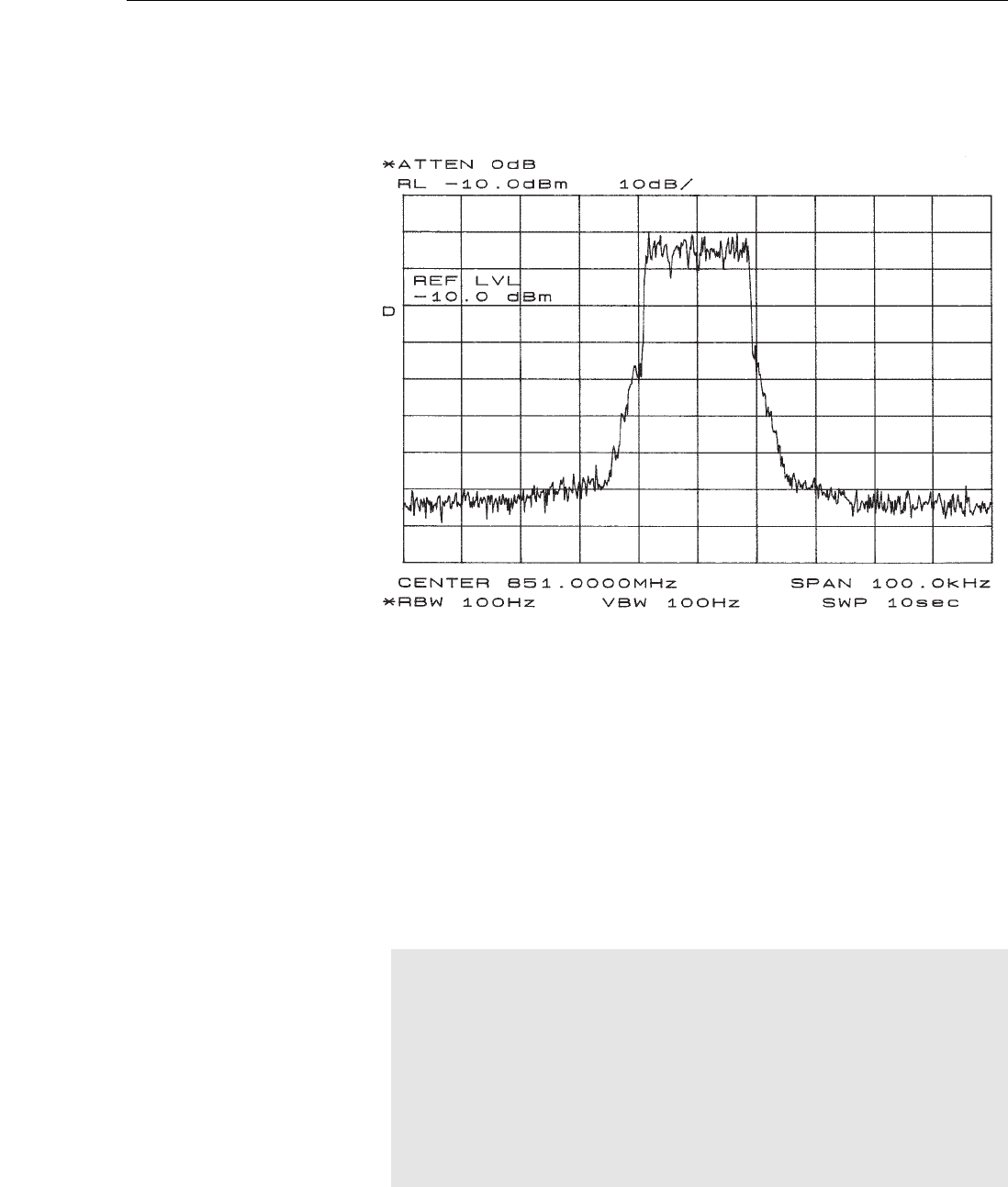
68P81095E02-D 4/1/2000 8-15
EBTS System Manual - Vol 2 800/900/1500 MHz Base Radios
Station Verification Procedures
Transmitter Verification Procedure
(70W, 800 MHz Power Amplifiers – CTF1040)
This procedure provides commands and responses to verify proper operation of
the transmit path for 800 MHz Base Radios using a 70 Watt Power AmpliÞer.
1. Apply power to the Base Radio by setting the switch to the 1 position.
The following message displays on the service computer during power-up.
Figure:8-3
Transmitted Signal Spectrum (800 MHz BR)
EBTS071
032394JNM
Base Radio
firmware revision RXX.XX.XX
Copyright 1998
Motorola, Inc. All rights reserved.
Unauthorized access prohibited
Enter login password:

8-16 68P81095E02-D 4/1/2000
800/900/1500 MHz Base Radios EBTS System Manual - Vol 2
Station Verification Procedures
2. Enter the proper password. After entering the correct password, the BRC>
prompt is displayed on the service computer.
The default password is motorola
NOTE
Motorola recommends that you change the default
password once proper operation of the equipment is
veriÞed.
3. At the BRC> prompt, type: dekey
This command veriÞes that there is no RF power being transmitted.
CAUTION
The following command keys the transmitter. Make
sure that transmission only occurs on licensed
frequencies or into an RF load.
BRC> dekey
XMIT OFF INITIATED

68P81095E02-D 4/1/2000 8-17
EBTS System Manual - Vol 2 800/900/1500 MHz Base Radios
Station Verification Procedures
4. At the BRC> prompt, type: set tx_power 70
This command sets the transmitter output to 70 Watts.
After keying the Base Radio, verify the forward and reßected powers of the
station along with the station VSWR with the parameters listed in Table 8-3.
5. At the BRC> prompt, type: get fwd_pwr
This command returns the current value of forward power from the RF
Power AmpliÞer.
Table 8-3
70W, 800 MHz PA Transmitter Parameters
Parameter Value or Range
Forward Power Greater than 66.5 Watts
Reßected Power Less than 7.0 Watts
VSWR Less than 2:1
BRC> set tx_power 70
setting transmitter power to 70 watts
TXLIN ATTENUATION: 5.000000
TARGET POWER: 70.00 watts [48.45 dBm]
ACTUAL POWER: 56.70 watts [47.54 dBm]
POWER WINDOW: 66.85 -> 73.30 watts [48.25 -> 48.65 dBm]
TXLIN LEVEL REGISTER REDUCED 85 STEPS [-3.32 dB].
TXLIN LEVEL: 0x55
completed successfully
BRC> get fwd_pwr
FORWARD POWER is 68.55 watts [48.36 dBm]

8-18 68P81095E02-D 4/1/2000
800/900/1500 MHz Base Radios EBTS System Manual - Vol 2
Station Verification Procedures
6. At the BRC> prompt, type: get ref_pwr
This command returns the current value of reßected power from the RF
Power AmpliÞer.
7. At the BRC> prompt, type: get vswr
This command calculates the current Voltage Standing Wave Ratio (VSWR)
from the RF Power AmpliÞer.
8. At the BRC> prompt, type: get alarms
This command returns all active alarms of the Base Radio.
NOTE
If the get alarms command displays alarms, refer to
the System Troubleshooting section of this manual for
corrective actions.
9. View the spectrum of the transmitted signal on the R2660 Communications
Analyzer in the Spectrum Analyzer mode. Figure 8-4 shows a sample of the
spectrum.
10. At the BRC> prompt, type: dekey
This command stops all transmitter activity.
BRC> get ref_pwr
REFLECTED POWER is 2.10 watts [33.22 dBm]
BRC> get vswr
VSWR is 1.42:1
BRC> get alarms
NO ALARM CONDITIONS DETECTED
BRC> dekey
XMIT OFF INITIATED
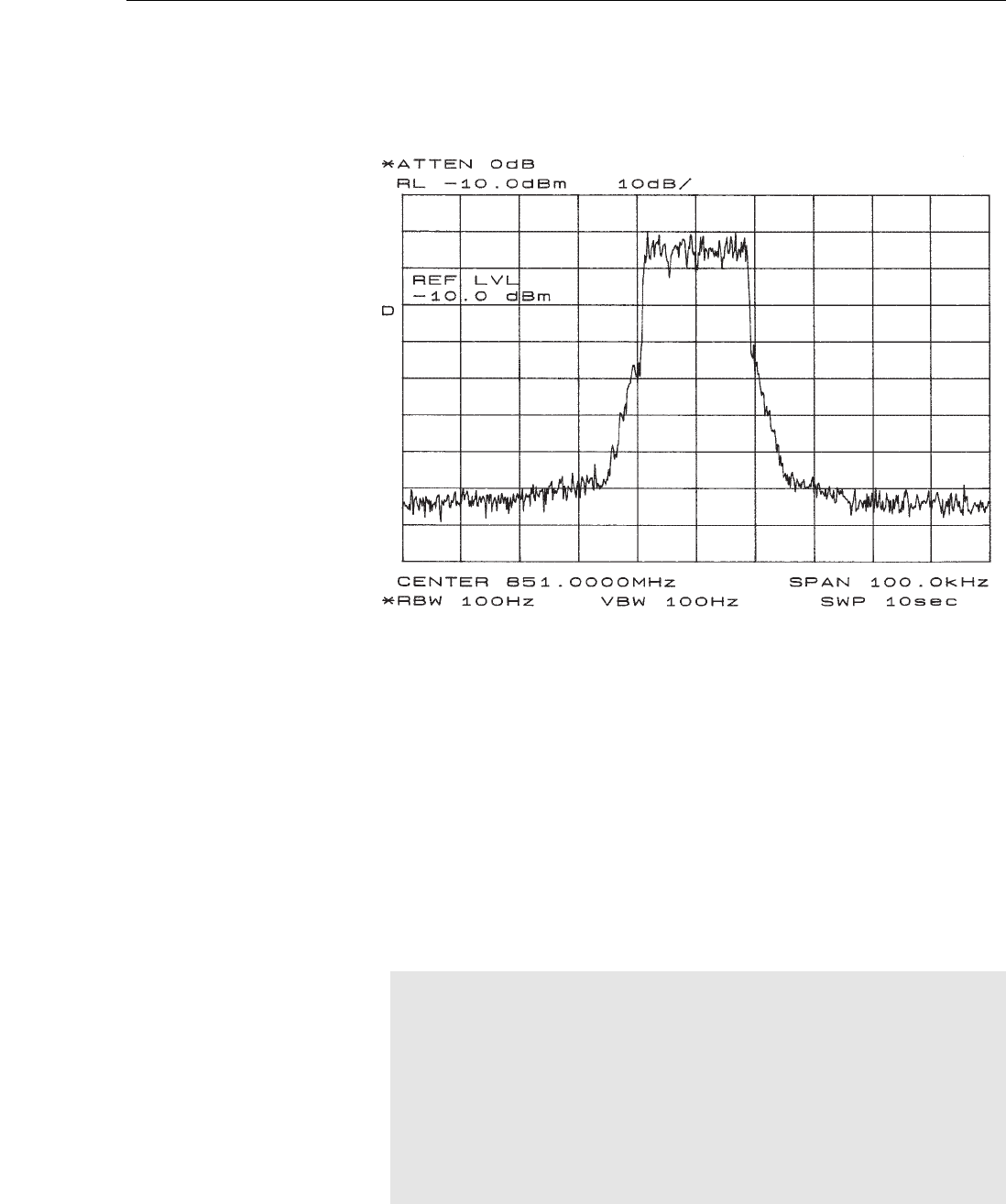
68P81095E02-D 4/1/2000 8-19
EBTS System Manual - Vol 2 800/900/1500 MHz Base Radios
Station Verification Procedures
Transmitter Verification Procedure
(60W, 900 MHz Power Amplifier – CLN1355)
This procedure provides commands and responses to verify proper operation of
the transmit path for 900 MHz Base Radios using 60 Watt Power AmpliÞer,
CLN1355 (kit no. CTF1300).
1. Apply power to the Base Radio by setting the switch to the 1 position.
The following message displays on the service computer during power-up.
Figure:8-4
Transmitted Signal Spectrum (800 MHz BR)
EBTS071
032394JNM
Base Radio
firmware revision RXX.XX.XX
Copyright 1998
Motorola, Inc. All rights reserved.
Unauthorized access prohibited
Enter login password:

8-20 68P81095E02-D 4/1/2000
800/900/1500 MHz Base Radios EBTS System Manual - Vol 2
Station Verification Procedures
2. Enter the proper password. After entering the correct password, the BRC>
prompt is displayed on the service computer.
The default password is motorola
NOTE
Motorola recommends that you change the default
password once proper operation of the equipment is
veriÞed.
3. At the BRC> prompt, type: dekey
This command veriÞes that there is no RF power being transmitted.
CAUTION
The following command keys the transmitter. Make
sure that transmission only occurs on licensed
frequencies or into an RF load.
BRC> dekey
XMIT OFF INITIATED

68P81095E02-D 4/1/2000 8-21
EBTS System Manual - Vol 2 800/900/1500 MHz Base Radios
Station Verification Procedures
4. At the BRC> prompt, type: set tx_power 60
This command sets the transmitter output to 60 Watts.
After keying the Base Radio, verify the forward and reßected powers of the
station along with the station VSWR with the parameters listed in Table 8-4.
5. At the BRC> prompt, type: get fwd_pwr
This command returns the current value of forward power from the RF
Power AmpliÞer.
Table 8-4
60W, 900 MHz PA – CLN1355 Transmitter Parameters
Parameter Value or Range
Forward Power Greater than 58.0 Watts
Reßected Power Less than 6.0 Watts
VSWR Less than 2:1
BRC> set tx_power 60
setting transmitter power to 60 watts
TXLIN ATTENUATION: 5.000000
TARGET POWER: 60.00 watts [47.78 dBm]
ACTUAL POWER: 56.70 watts [47.54 dBm]
POWER WINDOW: 57.30 -> 62.85 watts [47.58 -> 47.98 dBm]
TXLIN LEVEL REGISTER REDUCED 85 STEPS [-3.32 dB].
TXLIN LEVEL: 0x55
completed successfully
BRC> get fwd_pwr
FORWARD POWER is 61.0 watts [47.88 dBm]

8-22 68P81095E02-D 4/1/2000
800/900/1500 MHz Base Radios EBTS System Manual - Vol 2
Station Verification Procedures
6. At the BRC> prompt, type: get ref_pwr
This command returns the current value of reßected power from the RF
Power AmpliÞer.
7. At the BRC> prompt, type: get vswr
This command calculates the current Voltage Standing Wave Ratio (VSWR)
from the RF Power AmpliÞer.
8. At the BRC> prompt, type: get alarms
This command returns all active alarms of the Base Radio.
NOTE
If the get alarms command displays alarms, refer to
the System Troubleshooting section of this manual for
corrective actions.
9. View the spectrum of the transmitted signal on the R2660 Communications
Analyzer in the Spectrum Analyzer mode. Figure 8-5 shows a sample of the
spectrum.
10. At the BRC> prompt, type: dekey
This command stops all transmitter activity.
BRC> get ref_pwr
REFLECTED POWER is 1.67 watts [32.22 dBm]
BRC> get vswr
VSWR is 1.42:1
BRC> get alarms
NO ALARM CONDITIONS DETECTED
BRC> dekey
XMIT OFF INITIATED
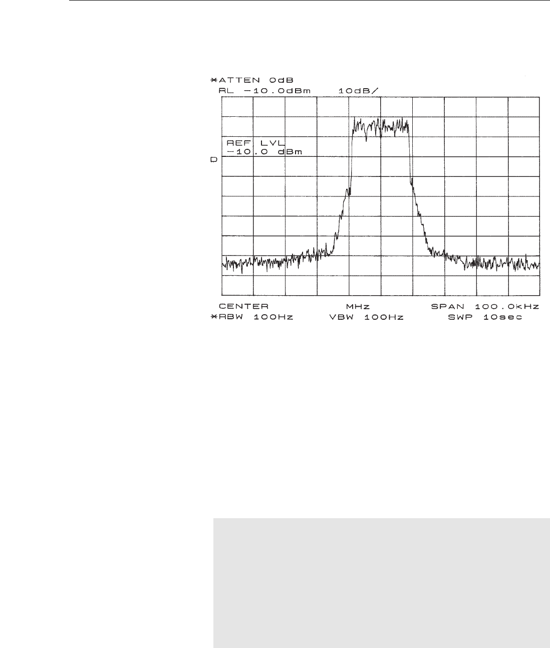
68P81095E02-D 4/1/2000 8-23
EBTS System Manual - Vol 2 800/900/1500 MHz Base Radios
Station Verification Procedures
Transmitter Verification Procedure
(40W, 1500 MHz Power Amplifier – TLN3426)
This procedure provides commands and responses to verify proper operation of
the transmit path for 1500 MHz Base Radios using a 40 Watt Power AmpliÞer.
1. Apply power to the Base Radio by setting the switch to the 1 position.
The following message displays on the service computer during power-up.
EBTS071
032394JNM
937.5000
EBTS418
101797JNM
Figure:8-5
Transmitted Signal Spectrum (900 MHz BR)
Base Radio
firmware revision RXX.XX.XX
Copyright 1998
Motorola, Inc. All rights reserved.
Unauthorized access prohibited
Enter login password:

8-24 68P81095E02-D 4/1/2000
800/900/1500 MHz Base Radios EBTS System Manual - Vol 2
Station Verification Procedures
2. Enter the proper password. After entering the correct password, the BRC>
prompt is displayed on the service computer.
The default password is motorola
NOTE
Motorola recommends that you change the default
password once proper operation of the equipment is
veriÞed.
3. At the BRC> prompt, type: dekey
This command veriÞes that there is no RF power being transmitted.
CAUTION
The following command keys the transmitter. Make
sure that transmission only occurs on licensed
frequencies or into a RF load.
BRC> dekey
XMIT OFF INITIATED

68P81095E02-D 4/1/2000 8-25
EBTS System Manual - Vol 2 800/900/1500 MHz Base Radios
Station Verification Procedures
4. At the BRC> prompt, type: set tx_power 40
This command sets the transmitter output to 40 Watts.
After keying the Base Radio, verify the forward and reßected powers of the
station along with the station VSWR with the parameters listed in Table 8-5.
5. At the BRC> prompt, type: get fwd_pwr
This command returns the current value of forward power from the RF
Power AmpliÞer.
Table 8-5
40W, 1500 MHz PA Transmitter Parameters
Parameter Value or Range
Forward Power Greater than 38.0 Watts
Reßected Power Less than 4.0 Watts
VSWR Less than 2:1
BRC> set tx_power 40
setting transmitter power to 40 watts
TXLIN ATTENUATION: 5.000000
TARGET POWER: 40.00 watts [46.02 dBm]
ACTUAL POWER: 28.38 watts [44.53 dBm]
POWER WINDOW: 38.20-> 41.89 watts [45.82 -> 46.22 dBm]
TXLIN LEVEL REGISTER REDUCED 59 STEPS [-2.30 dB].
TXLIN LEVEL: 0x6f
completed successfully
BRC> get fwd_pwr
FORWARD POWER is 39.13 watts [45.92 dBm]

8-26 68P81095E02-D 4/1/2000
800/900/1500 MHz Base Radios EBTS System Manual - Vol 2
Station Verification Procedures
6. At the BRC> prompt, type: get ref_pwr
This command returns the current value of reßected power from the RF
Power AmpliÞer.
7. At the BRC> prompt, type: get vswr
This command calculates the current Voltage Standing Wave Ratio (VSWR)
from the RF Power AmpliÞer.
8. At the BRC> prompt, type: get alarms
This command returns all active alarms of the Base Radio.
NOTE
If the get alarms command displays alarms, refer to
the System Troubleshooting section of this manual for
corrective actions.
9. View the spectrum of the transmitted signal on the R2660 Communications
Analyzer in the Spectrum Analyzer mode. Figure 8-3 shows a sample of the
spectrum.
10. At the BRC> prompt, type: dekey
This command stops all transmitter activity.
BRC> get ref_pwr
REFLECTED POWER is 0.27 watts [24.28 dBm]
BRC> get vswr
VSWR is 1.17:1
BRC> get alarms
NO ALARM CONDITIONS DETECTED
BRC> dekey
XMIT OFF INITIATED
68P81095E02-D 4/1/2000 8-27
EBTS System Manual - Vol 2 800/900/1500 MHz Base Radios
Station Verification Procedures
Figure:8-6
Transmitted Signal Spectrum (1500 MHz BR)

8-28 68P81095E02-D 4/1/2000
800/900/1500 MHz Base Radios EBTS System Manual - Vol 2
Station Verification Procedures
Equipment Disconnection
Use the following steps to disconnect equipment after verifying the transmitter.
1. Remove power from the Base Radio by setting the Power Supply rocker
switch (located behind the front panel of the Power Supply) to the OFF (0)
position.
2. Disconnect the RS-232 cable from the connector on the service computer.
3. Disconnect the other end of the RS-232 cable from the RS-232 connector
located on the front panel of the BRC.
4. Disconnect the test cable from the PA OUT connector located on the
backplane of the Base Radio.
5. Connect the standard equipment cable to the PA OUT connector.
6. Disconnect the 10 dB attenuator from the other end of the test cable.
7. From the attenuator, disconnect the cable to the R2660
Communications Analyzer.
8. Restore power to the Base Radio by setting the Power Supply rocker switch
to the ON (1) position.
If necessary, continue with the Receiver VeriÞcation Procedure.
Receiver Verification
The receiver veriÞcation procedure sends a known test signal to the Base Radio to
verify the receive path. This veriÞcation procedure is recommended after
replacing a Receiver, BRC, or Power Supply module.
NOTE
The following procedure requires the Base Radio to be
out of service. Unless the Base Radio is currently out
of service, Motorola recommends performing this
procedure during off-peak hours. This minimizes or
eliminates disruption of service to system users.
Equipment Setup
Set up the equipment for the receiver veriÞcation procedure as follows:
1. Remove power from the Base Radio by setting the Power Supply rocker
switch (located behind the front panel of the Power Supply) to the OFF (0)
position.
2. Connect one end of the RS-232 cable to the service computer.

68P81095E02-D 4/1/2000 8-29
EBTS System Manual - Vol 2 800/900/1500 MHz Base Radios
Station Verification Procedures
3. Connect the other end of the RS-232 cable to the STATUS port located on the
front panel of the BRC.
4. Disconnect the existing cable from the connector labeled RX1 (or the
connector corresponding to the receiver under test).
This connector is located on the backplane of the Base Radio.
5. Connect a test cable to the RX 1 connector.
6. Connect the other end of the test cable to the RF IN/OUT connector on the
R2660 Communications Analyzer.
7. Remove power from the R2660 and connect the Rubidium Frequency
Standard 10MHZ OUTPUT to a 10 dB attenuator.
8. Connect the other end of the 10 dB attenuator to the 10MHZ REFERENCE
OSCILLATOR IN/OUT connector on the R2660.
9. Set the R2660 to the EXT REF mode.
10. Apply power to the R2660.
NOTE
Refer to the equipment manual provided with the
R2660 for further information regarding mode
conÞguration of the unit (Motorola Part
No. 68P80386B72).
11. Set the R2660 to the receive frequency of the Base Radio under test.
All receivers within a single Base Radio have the same receive frequency.
12. Set the R2660 to generate the test signal at an output level of -80dBm.
Receiver Verification Procedure
This procedure provides commands and responses to verify proper operation of
the Base Radio receive path. Perform the procedure on all three receivers in each
Base Radio in the EBTS.
The Bit Error Rate (BER) measurement meets speciÞcations at less than 0.01%
(1.0e-02%) to pass the process.
Before you begin the veriÞcation procedure, put the Base Radio into the test mode
of operation to take it out of service. Enable the desired receiver under test and
disable the other receiver(s). In this case the receiver under test is receiver #1.
In the following procedures, enter the software commands as they appear after
the prompt. These commands are in bold letters.
For example, BRC> get rx_freq

8-30 68P81095E02-D 4/1/2000
800/900/1500 MHz Base Radios EBTS System Manual - Vol 2
Station Verification Procedures
13. Restore power to the Base Radio by setting the Power Supply rocker switch
to the ON (1) position.
The following message displays on the service computer during power-up.
14. Enter the proper password. After entering the correct password, the BRC>
prompt is displayed on the service computer.
The default password is motorola
NOTE
Motorola recommends that you change the default
password once proper operation of the equipment
is veriÞed.
Base Radio
firmware revision RXX.XX.XX
Copyright 1998
Motorola, Inc. All rights reserved.
Unauthorized access prohibited
Enter login password:

68P81095E02-D 4/1/2000 8-31
EBTS System Manual - Vol 2 800/900/1500 MHz Base Radios
Station Verification Procedures
15. At the BRC> prompt, type: get rx_freq
This command displays the receive frequency for the current Base Radio.
For 800/900/1500 MHz Base Radios, the message respectively appears as:
800 MHz BR:
900 MHz BR:
1500 MHz BR:
16. Verify that the R2660 transmit frequency is set to the frequency determined
in the previous step.
17. At the BRC> prompt, type: set rx_mode 1
This command is used to enable the antenna/receiver under test.
BRC> get rx_freq
The RX FREQUENCY is: 806.00000
BRC> get rx_freq
The RX FREQUENCY is: 896.000
BRC> get rx_freq
The RX FREQUENCY is: 1453.000
BRC>set rx_mode 1
set RECEIVER 1 to ENABLED in RAM
set RECEIVER 2 to DISABLED in RAM
set RECEIVER 3 to DISABLED in RAM

8-32 68P81095E02-D 4/1/2000
800/900/1500 MHz Base Radios EBTS System Manual - Vol 2
Station Verification Procedures
18. At the BRC> prompt, type: get rssi 1 1000
This commands returns the receive signal strength indication. To pass the
BER ßoor test, the Bit Error Rate must be less than 0.01% (1.0e-02%) for the
displayed results.
19. Verify that the RSSI dBm signal strength, for the receiver under test, is
-80.0 dBm ± 1.0 dBm. Adjust the R2660 signal output level to get the
appropriate RSSI dBm level. The BER ßoor % value is valid only if the RSSI
signal strength is within the limits of -81.0 dBm to -79.0 dBm.
20. At the BRC > prompt, type: get alarms
This command returns all active alarms of the Base Radio.
NOTE
If the get alarms command displays alarms, refer to
the System Troubleshooting section for corrective
actions.
BRC> get rssi 1 1000
Starting RSSI monitor for 1 repetitions averaged each 1000 reports.
Line RSSI1 RSSI2 RSSI3 SGC CI BER OffsetSyncMiss
dBm dBm dBm dB dBmdBm % Hz%
---- ------ ------ ------ ---- --------------------- ------- ---------
0 -80.0 -131.5 -131.5 0 -79.2 -121.90.000e+00-5.4.000e+00
BRC> get alarms
NO ALARM CONDITIONS DETECTED

68P81095E02-D 4/1/2000 8-33
EBTS System Manual - Vol 2 800/900/1500 MHz Base Radios
Station Verification Procedures
21. At the BRC> prompt, type: get rx1_kit_no
As shown below respectively for 800 /900/1500 MHz Base Radios, this
command returns the kit number of the receiver.
800 MHz BR:
900 MHz BR:
1500 MHz BR:
NOTE
If the kit number is CRF6010 or CRF6030, continue to
step 22, otherwise to Equipment Disconnection.
22. At the BRC> prompt, type: get rx_fru_config
This command lists the receivers active for diversity.
NOTE
If the antenna conÞguration does not match the
receiver conÞguration, use the set rx_fru_config
MMI command to properly set the parameter.
BRC> get rx1_kit_no
RECEIVER 1 KIT NUMBER IS CRF6010A
BRC> get rx1_kit_no
RECEIVER 1 KIT NUMBER IS CRF6030A
BRC> get rx1_kit_no
RECEIVER 1 KIT NUMBER IS CRX1020B
BRC> get rx_fru_config
RECEIVER CONFIGURATION {RX1 RX2 RX3}

8-34 68P81095E02-D 4/1/2000
800/900/1500 MHz Base Radios EBTS System Manual - Vol 2
Station Verification Procedures
Equipment Disconnection
Disconnect equipment after verifying the receiver as follows:
1. Remove power from the Base Radio by setting the Power Supply rocker
switch (located behind the front panel of the Power Supply) to the OFF (0)
position.
2. Disconnect the RS-232 cable from the connector on the service computer.
3. Disconnect the other end of the RS-232 cable from the RS-232 connector on
the front panel of the BRC.
4. Disconnect the test cable from the RX 1 connector located on the backplane
of the Base Radio.
5. Connect the standard equipment cable to the RX 1 connector.
6. Disconnect the cable to the R2660 Communications Analyzer.
7. Restore power to the Base Radio by setting the Power Supply rocker switch
to the ON (1) position.
This completes the Receiver VeriÞcation Procedure for the receiver under
test.
Repeat the Receiver VeriÞcation Procedure for each receiver in every Base Radio
in the EBTS.

68P81095E02-D 4/1/2000 8-35
EBTS System Manual - Vol 2 800/900/1500 MHz Base Radios
Single Channel BR Backplane
Single Channel BR Backplane
Backplane Connectors
All external equipment connections are made on the Base Radio backplane.
Table 8-6 lists and describes each of the connectors on the backplane.
Table 8-6
Base Radio Backplane Connectors
Connector Description Type
RX 1 through RX 3 Provides the input path for the received signal to the
Base Radio. Each receiver has an input for one of these
signals.
Connect these ports to a multicoupler distribution
system and surge protection circuitry before connecting
them to the receive antennas.
RF-type
connector in
Table 8
EX OUT/EX FB
PA IN/PA FB
Connects the exciter and PAs together to form the
transmitter for the Base Radio. These connections are
usually made at the factory
These four ports close the feedback loop between these
two modules by connecting EX OUT to the PA IN and
the EX FB to the PA FB
RF-type
connectors
in Table 21
and Table 22
PA OUT Transmits the RF output of the Base Radio. Connect this
port to a combiner or duplexer before connecting to the
transmit antenna
RF-type
connector in
Table 22
ETHERNET A
(or labeled
ETHERNET on
some production
units)
Provides Ethernet connectivity to the Base Radio from
the site controller. This Ethernet port connects directly
to the BRC
BNC-type
connector in
Table 18
5MHZ/ 1 PPS-A
(or labeled SPARE
on some
production units)
Serves as both the timing and frequency reference port
for the Base Radio
This port is connected to the site timing/frequency
reference.
BNC-type
connector in
Table 20
RS-232 This is a DTE RS-232 interface provided for future use
and is not currently enabled
DB-9-type
connectors
in Table 17
ALARM Provides the connection for external calibrated power
monitors to the Base Radio
This connector also provides station DC voltages and
programming lines (SPI) for monitoring/potential
future expansion
DB-25-type
connector
AC POWER Provides connection to AC power supply, if the Base
Radio is equipped with an AC power supply
Line cord
connector
DC POWER Provides DC power connection, if the Base Radio is
equipped with a DC power supply or an AC power
supply to support the battery revert feature
Card edge
connector
GROUND Connects the station to ground. A ground stud and a
ground braid on the back of the Base Radio connect the
station to a site ground, such as an appropriately
grounded cabinet
This ground provides increased transient/surge
protection for the station
Ground stud
8-36 68P81095E02-D 4/1/2000
800/900/1500 MHz Base Radios EBTS System Manual - Vol 2
Single Channel BR Backplane
Figure 8-7 shows the locations of the Base Radio external connections.
Backplane RF Connections
When Base Radios are shipped from the factory as FRUs, each connection on the
back of a repeater has a designated color dot beside it as listed in Table 8-7. To
Þnd where a cable should be connected, match the label wrapped around the
cable to the dot on the back of the repeater.
Table 8-7
Color Codes for RF Connections on Rear of Base Radio
Connectors Color Dot Code
TX Orange
RX 1 Red
RX 2 Green
RX 3 Yellow
Ethernet White
5 MHz/1 pps A
or Spare
Gray
EX OUT
PA IN
EX
PA FB
DC POWER
AC POWER
RS 232ALARM
5MHZ/1 PPS B
RX 1
RX 2
RX 3
5MHZ/1 PPS A
ETHERNET A
PA OUT
GROUND
EBTS327
021997JNM
RE BLACK
This port must be terminated by 50Ω load when configured for
2 Branch Diversity. Also, the rx_fru_config parameter must be set to R12.
*
*
Figure:8-7
Base Radio Backplane Connectors

68P81095E02-D 4/1/2000 8-37
EBTS System Manual - Vol 2 800/900/1500 MHz Base Radios
Single Channel BR Backplane
Backplane Connector Pinouts
Table 8 lists the pin-outs for the 96-pin P1 connector
of the Base Radio Controller board.
Table 12 lists the pin-outs for the 96-pin P1
connector for Receiver 1.
Table 8
P1 Connector Pin-outs
Pin No. Row A Row B Row C
1 AGC3 14.2V AGC1
2 AGC4 14.2V AGC2
3 GND GND GND
4 RESET GND GND
5 BATT_STAT GND GND
6 CTS GND GND
7 RTS 5V 5V
85V 5V 5V
95V 5V 5V
10 SHUTDOWN 5V
11 RCLK 5V DATA1
12 ODC_1 5V DATA1*
13 TCLK GND DATA3
14 ODC_3 GND DATA3*
15 RXD GND DATA2
16 ODC_2 DATA2*
17 TXD
18 SSI SBI_1
19 SSI* SBI_3
20 BRG GND SBI_2
21 CLK
22 CLK* GND A4
23 GND A3
24 A5 GND A2
25 A0 GND A1
26 CD GND 5MHZ/
SPARE
27 METER_STAT GND SPI_MISO
28 WP* GND SPI_CLK
29 GND GND SPI_MOSI
30 GND GND GD
31 1PPS_GPS GND 2.1MHZ_TX
32 GND GND 2.1MHZ_RX
NOTE: * = enabled low
Table 9
P1 Connector Pin-outs
Pin No. Row A Row B Row C
1 AGC3 GND AGC1
2 AGC4 GND AGC2
3 GND GND GND
4 GND GND GND
5 14.2V 14.2V 14.2V
6 14.2V 14.2V 14.2V
7 GND GND GND
8 GND GND GND
9 5V5V5V
10 5V 5V 5V
11 GND GND GND
12 GND GND GND
13 DATA1* GND GND
14 DATA1 GND GND
15 ODC_1 GND GND
16 GND GND GND
17 GND GND GND
18 SBI_1 GND GND
19 GND GND GND
20 GND GND GND
21 A0_CS1
22 A1_CS2
23 A5
24 WP*
25 A4_RXSEL
26
27 SPI_MISO
28 SPI_MOSI
29 SPI_CLK
30 GND GND GND
31 GND GND GND
32 GND GND 2.1MHZ_RX
NOTE: * Enabled low

8-38 68P81095E02-D 4/1/2000
800/900/1500 MHz Base Radios EBTS System Manual - Vol 2
Single Channel BR Backplane
Table 13 lists the pin-outs for the 96-pin P2
connector for Receiver 2.
Table 11 lists the pin-outs for the 96-pin P3 connector
for Receiver 3.
Table 10
P2 Connector Pin-outs
Pin No. Row A Row B Row C
1 AGC3 GND AGC1
2 AGC4 GND AGC2
3 GND GND GND
4 GND GND GND
5 14.2V 14.2V 14.2V
6 14.2V 14.2V 14.2V
7 GND GND GND
8 GND GND GND
9 5V5V5V
10 5V 5V 5V
11 GND GND GND
12 GND GND GND
13 DATA2* GND GND
14 DATA2 GND GND
15 ODC_2 GND GND
16 GND GND GND
17 GND GND GND
18 SBI_2 GND GND
19 GND GND GND
20 GND GND GND
21 A0_CS1
22 A1_CS2
23 A5
24 WP*
25 A3_RXSEL
26
27 SPI_MISO
28 SPI_MOSI
29 SPI_CLK
30 GND GND GND
31 GND GND GND
32 GND GND 2.1MHZ_RX
NOTE: * Enabled low
Table 11
P3 Connector Pin-outs
Pin No. Row A Row B Row C
1 AGC3 GND AGC1
2 AGC4 GND AGC2
3 GND GND GND
4 GND GND GND
5 14.2V 14.2V 14.2V
6 14.2V 14.2V 14.2V
7 GND GND GND
8 GND GND GND
9 5V5V5V
10 5V 5V 5V
11 GND GND GND
12 GND GND GND
13 DATA3* GND GND
14 DATA3 GND GND
15 ODC_3 GND GND
16 GND GND GND
17 GND GND GND
18 SBI_3 GND GND
19 GND GND GND
20 GND GND GND
21 A0_CS1
22 A1_CS2
23 A5
24 WP*
25 A2_RXSEL
26
27 SPI_MISO
28 SPI_MOSI
29 SPI_CLK
30 GND GND GND
31 GND GND GND
32 GND GND 2.1MHZ_RX
NOTE: * Enabled low

68P81095E02-D 4/1/2000 8-39
EBTS System Manual - Vol 2 800/900/1500 MHz Base Radios
Single Channel BR Backplane
Table 12 lists the pin-outs for the 48-pin P2
connector of the 3X Receiver.
Table 13 lists the pin-outs for the 16-pin P3
connector of the 3X Receiver.
Table 14 lists the pin-outs for the 96-pin P5
connector of the Exciter.
Table 12
P2 Connector Pin-outs
Pin
No. Row A Row B Row C Row D
1 GND AGC4 AGC3 GND
2 GND AGC2 AGC1 A0
3 GND RX1_DAT
A
RX1_DAT
A
A1
4 GND RX1_SBI RX1_ODC A2
5 GND RX2_DAT
A
RX2_DAT
A
A3
6 5V RX2_SBI RX2_ODC A4
7 GND RX3_DAT
A
RX3_DAT
A
A5
8 GND RX3_SBI RX3_ODC WP*
9 14.2V SCLK MOSI MISO
10 14.2V GND GND GND
11 14.2V GND REF GND
12 GND GND GND GND
NOTE: Row A is make first, break last.
Table 13
P3 Connector Pin-outs
Pin
No. Row
ARow B Row C Row
DRow E
1 GND GND GND
2 RX1
3 GND GND GND
4
5
6
7 GND GND GND
8 RX2 RX3
9 GND GND GND
Table 14
P5 Connector Pin-outs
Pin No. Row A Row B Row C
1 28V 28V 28V
2 28V 28V 28V
3 14.2V 14.2V 14.2V
4 14.2V 14.2V 14.2V
55V5V5V
65V5V5V
7 GND GND EXT_VFWD
8 GND GND EXT_VREF
9
10 GND GND GND
11 GND GND VBLIN
12 GND GND RESET
13
14 GND GND GND
15 GND GND SPI_MISO
16 A0 GND GND
17 GND GND SPI_CLK
18 A1 GND WP*
19 GND GND GND
20 A5 GND SPI_MOSI
21 GND GND GND
22 A4 GND GND
23 GND GND CLK*
24 A3 GND GND
25 GND GND CLK
26 GND GND GND
27 GND GND SSI*
28 GND GND GND
29 GND GND SSI
30 GND GND GND
31 GND GND 2.1MHz_TX
32 GND GND GND
NOTE: * = enabled low

8-40 68P81095E02-D 4/1/2000
800/900/1500 MHz Base Radios EBTS System Manual - Vol 2
Single Channel BR Backplane
Table 15 lists the pin-outs for the 96-pin P6
connector of the Power AmpliÞer.
Table 16 lists the pin-outs for the 25-pin P7 Alarm
Table 17 lists the pin-outs for the 9-pin P8
RS-232 connector.
Table 18 lists the pin-outs for P13. Tables 19
through 22 list the pin-outs for the SMA and
blindmate connectors for Receivers 1- 3, BRC,
Exciter and PA.
Table 23 lists the pin-outs for 78-pin P9 connector of
the Power Supply.
Table 15
P6 Connector Pin-outs
Pin No. Row A Row B Row C
1 VBLIN GND 28V
2 GND GND 28V
3 A0 GND 28V
4 GND GND 28V
5 A1 GND 28V
6 GND GND 28V
7 A2 GND 28V
8 GND GND 28V
9 A3 GND 28V
10 GND GND 28V
11 SPI_MISO GND 28V
12 GND GND 28V
13 SPI_MOSI GND 28V
14 GND GND 28V
15 SPI_CLK GND 28V
16 GND GND 28V
17 WP* GND 28V
18 GND GND 28V
19 GND GND 28V
20 GND GND 28V
21 GND GND 28V
22 GND GND 28V
23 GND GND 28V
24 GND GND 28V
25 GND 5V 28V
26 GND 5V 28V
27 GND 14.2V 28V
28 GND 14.2V 28V
29 GND 14.2V 28V
30 GND 14.2V 28V
31 GND 28V 28V
32 GND 28V 28V
NOTE: * = enabled low
Table 16
P7 Connector Pin-outs
Pin No. Signal
1 SPI_MISO
2 SPI_MOSI
3 SPI_CLK
4A0
5A1
6A2
7A3
8A4
9A5
10 GND
11 28V
12 14.2V
13 14.2V
14 WP*
15 5V
16 GND
17 BATT_STAT
18 MTR_STAT
19 EXT_VFWD
20 EXT_VREF
21 GND
22 GND
23 BAT_TEMP
24 VAT_TEMP
25 GND
NOTE: * = enabled low

68P81095E02-D 4/1/2000 8-41
EBTS System Manual - Vol 2 800/900/1500 MHz Base Radios
Single Channel BR Backplane
Table 17
P8 Connector Pin-outs
Pin No. Signal
1CD
2 RxD
3 TxD
4 RCLK
5 GND
6 TCLK
7RTS
8 CTS
9 BRG
Table 18
P13 Connector Pin-outs
Connector Signal
1 ETHERNET - A (or 5MHZ IN*)
* May appear as indicated in parenthesis on some production
units.
Table 19
SMA Connectors- Receivers
Connector Signal
P19 RCV ONE RF IN
P20 RCV TWO RF IN
P21 RCV THREE RF IN
Table 20
Blind Mates - BRC
Connector Signal
P10 SPARE* (or 5MHZ/1 PPS - A)
P11 ETHERNET* (or ETHERNET - A)
*May appear as indicated in parenthesis on some production
units.
Table 21
Blind Mates - Exciter
Connector Signal
P14 EXCITER OUT
P15 EXCITER FEEDBACK

8-42 68P81095E02-D 4/1/2000
800/900/1500 MHz Base Radios EBTS System Manual - Vol 2
Single Channel BR Backplane
Table 22
Blind Mates - PA
Connector Signal
P16 PA FEEDBACK
P17 PA IN
P18 PA RF OUT
Table 23
P9 Connector Pin-outs
Pin No. Signal
1 GND
2 GND
3 28V
4 28V
5 28V
6 28V
7 28V
8 28V
9 28V
10 28V
11 28V
12 28V
13 28V
14 28V
15 28V
16 14.2V
17 14.2V
18 14.2V
19 14.2V
20 14.2V
21 14.2V
22 14.2V
23 14.2V
24 5V
25 5V
26 5V
27 5V
28 5V
29 5V
30 5V
31 5V

68P81095E02-D 4/1/2000 8-43
EBTS System Manual - Vol 2 800/900/1500 MHz Base Radios
Single Channel BR Backplane
32 GND
33 GND
34 GND
35 GND
36 GND
37 GND
38 GND
39 GND
40 GND
41 GND
42 GND
43 GND
44 GND
45 GND
46 GND
47 GND
48 GND
49 GND
50 GND
51 GND
52 GND
53 GND
54 SCR_SHUT
55 SCR_THRESH
56 RELAY_ENABLE
57 SHUTDOWN
58 28V_AVG
59 BATT_TEMP
60 SPI_MISO
61 SPI_MOSI
62 SPI_CLK
63
64
65
66
67 A0(CS1)
68 A1(CS2)
Table 23
P9 Connector Pin-outs (Continued)
Pin No. Signal

8-44 68P81095E02-D 4/1/2000
800/900/1500 MHz Base Radios EBTS System Manual - Vol 2
Single Channel BR Backplane
69 A5
70
71 A4
72
73 A3
74 GND
75 A2
76 GND
77 GND
78 GND
Table 23
P9 Connector Pin-outs (Continued)
Pin No. Signal

68P81095E02-D 4/1/2000 8-45
EBTS System Manual - Vol 2 800/900/1500 MHz Base Radios
Single Channel BR Backplane
Base Radio Signals
Table 8-24 lists and describes the Base Radio signals.
Table 8-24
Base Radio Signal Descriptions
Signal Name Signal Description
GND Station ground
28V 28VDC
14.2V 14.2VDC
5.1V 5.1 VDC
A0,A1,A2,A3,A4,A5 The BRC uses these lines to address station modules and
devices on those modules
SPI_MOSI Serial Processor Interface - Master out slave in Data
SPI_MISO Serial Processor Interface - Master in slave out Data
SPI_CLK Serial Processor Interface - Clock signal (100 KHz - 1 MHz)
AGC1, AGC2, AGC3, AGC4 BRC uses these lines to set the digital attenuator's on the
receiver(s) for SGC functionality
2.1MHz_RX 2.1MHz generated on the BRC and used as a reference by
the Receiver(s)
2.1MHz_TX 2.1MHz generated on the BRC and used as a reference by
the Exciter
DATA1, DATA1* This differential pair carries receiver 1 data to the Base
Radio Controller
DATA2 DATA2* This differential pair carries receiver 2 data to the Base
Radio Controller
DATA3, DATA3* This differential pair carries receiver 3 data to the Base
Radio Controller
ODC_1, ODC_2, ODC_3 Clocks used to clock differential receive data from each
respective receiver to the BRC
SBI_1, SBI_2, SBI_3 Serial Bus Interface - These lines are used to program the
custom receiver IC on each receiver
SSI, SSI* Differential transmit data from the Exciter to the BRC
CLK, CLK* Differential Data clock used to clock transmit data from the
BRC to the Exciter
BRCVBLIN Programmable bias voltage generated on the Exciter and used to
bias the Power ampliÞer devices
VBLIN Programmable bias voltage generated on the Exciter and used
to bias the Power ampliÞer devices
RESET Output from BRC to Exciter (currently not used)
EXT_VFWD DC voltage representing the forward power at the antenna as
measured by the external wattmeter
EXT_VREF DC voltage representing the reßected power at the antenna as
measured by the external wattmeter
WP* Write protect line used by the BRC to write to serial EEPROMs
located on each module
BAT_STAT Binary ßag used to signal BRC to monitor the External battery
supply alarm

8-46 68P81095E02-D 4/1/2000
800/900/1500 MHz Base Radios EBTS System Manual - Vol 2
Single Channel BR Backplane
METER_STAT Binary ßag used by the BRC to indicate to the BRC it
should monitor
1PPS Global Positioning System - 1 pulse per second (this may be
combined with 5MHz at the site frequency reference
RCLK RS-232 - Receive clock
TCLK RS-232 - Transmit clock
CTS RS-232 - Clear to send
RTS RS-232 - Request to send
CD RS-232 - Carrier detect
RXD RS-232 - Receive data
TXD RS-232 - Transmit data
BRG RS-232 - Baud rate generator
5MHz / Spare signal currently not used
EXCITER_OUT Forward transmit path QQAM at approximately a 11dBm level
EXCITER_FEEDBACK Signal comes from the PA at approximately a 16dBm. Used to
close the cartesian RF_LOOP
PA_IN 4 dBm QQAM forward path of the transmitter
PA_FEEDBACK Signal to the Exciter at approximately 16dBm. Used to close the
cartesian RF_LOOP
RX1_IN RF into Receiver 1
RX2_IN RF into Receiver 2
RX3_IN RF into Receiver 3
5MHZ REFERENCE 5MHz station/site reference. Signal comes from the redundant
site frequency reference and usually is multiplexed with the
1PPS signal from the global positioning satellite input to the
site frequency reference
ETHERNET Interface between the BRC and the ACG. This connects the
Base to the 10 MHz LAN
SCR_SHUT Signal currently not used
SCR_THRESH Signal currently not used
RELAY ENABLE Signal currently not used
SHUTDOWN Input signal from the BRC to the Power supply. Used to
exercise a station "hard startÓ
28V_AVG Signal currently not used
BATT_TEMP DC voltage from the external batteries used to represent the
temperature of the batteries. Signal used only with AC
power supplies
NOTE: * = enabled low
Table 8-24
Base Radio Signal Descriptions (Continued)
Signal Name Signal Description

68P81095E02-D 12/12/2000
9
-
1
EBTS System Manual - Vol 2 800/900/1500 MHz Base Radios
9 Troubleshooting
QUAD Channel Base
Radios
Overview
This chapter is a guide for installing a Quad Base Radio and isolating Base Radio
failures to the FRU level. The chapter contains procedures for:
❐
Troubleshooting
❐
Installation
❐
VeriÞcation
❐
Station Operation
The Base Radio maintenance philosophy is repair by replacing defective FRUs
with new FRUs. This maintenance method limits down-time, and quickly
restores the Base Radio to normal operation.
Two Base Radio troubleshooting procedures appear here. Each procedure quickly
identifies faulty FRUs.
Ship defective FRUs to a Motorola repair depot for repair.
Recommended Test Equipment
Table 9-1 lists recommended test equipment for performing Base Radio
troubleshooting and veriÞcation procedures.

9-2
68P81095E02-D 12/12/2000
800/900/1500 MHz Base Radios EBTS System Manual - Vol 2
Table 9-1
Recommended Test Equipment
Test Equipment Model Number Use
Communications Analyzer R2660 w/iDEN option Used for checking receive and
transmit operation (iDEN
signaling capability) and station
alignment
Signal Generator HP4432b RX testing
Dummy Load (50
Ω
, 150 W
)
none Used to terminate output
3 way RF splitter none Used to connect Hp4432b to Base
radio
Service Computer IBM or clone, 80286 or
better
Local service terminal
Portable Rubidium
Frequency Standard
Ball Efratom Frequency standard for R2660,
netting TFR
Power Meter none Used to measure reßected and
forward power
RF Attenuator, 250 W, 10 dB Motorola 0180301E72 Protection for R2660
Software:
Communication
Quad BR waveform
Procomm Plus
Motorola supplied
Local service computer
with HP4432b
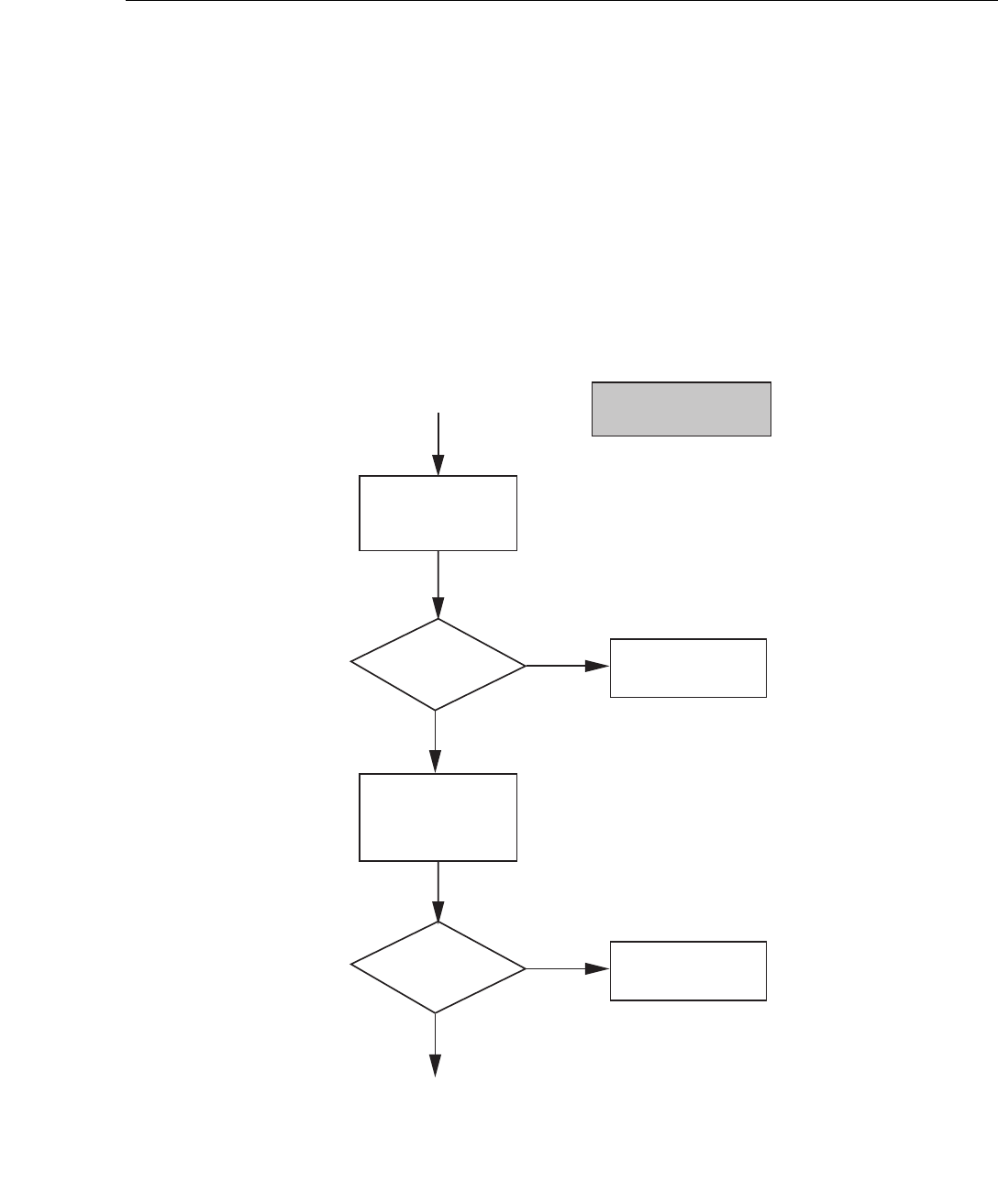
68P81095E02-D 12/12/2000
9
-
3
EBTS System Manual - Vol 2 800/900/1500 MHz Base Radios
Troubleshooting Procedures
Many troubleshooting and station operation procedures require Man-Machine
Interface (MMI) commands. These commands communicate station level
commands to the Base Radio via the RS-232 communications port on the front of
the BRC.
Routine Checkout
Procedure 1 is a quick, non-intrusive test performed during a routine site visit.
Use this procedure to verify proper station operation without taking the station
out of service. Figure 9-1 shows the Procedure 1 Troubleshooting Flowchart.
Figure:9-1
Procedure 1 Troubleshooting Flowchart
PROCEDURE 1
ROUTINE
SITE VISIT
OBSERVE LED
INDICATORS
Module Suspected
of Being Faulty?
No
No
DONE
CHECK CURRENT
ALARM STATUS
Use MMI command
get alarms
to check alarm status
Module Suspected
of Being Faulty?
Ye s Go to Troubleshooting
Procedure 2 Flow Chart
Ye s Go to Troubleshooting
Procedure 2 Flow Chart
Refer to
Controls and Indicators
for LED Definitions
EBTS021
071895JNM
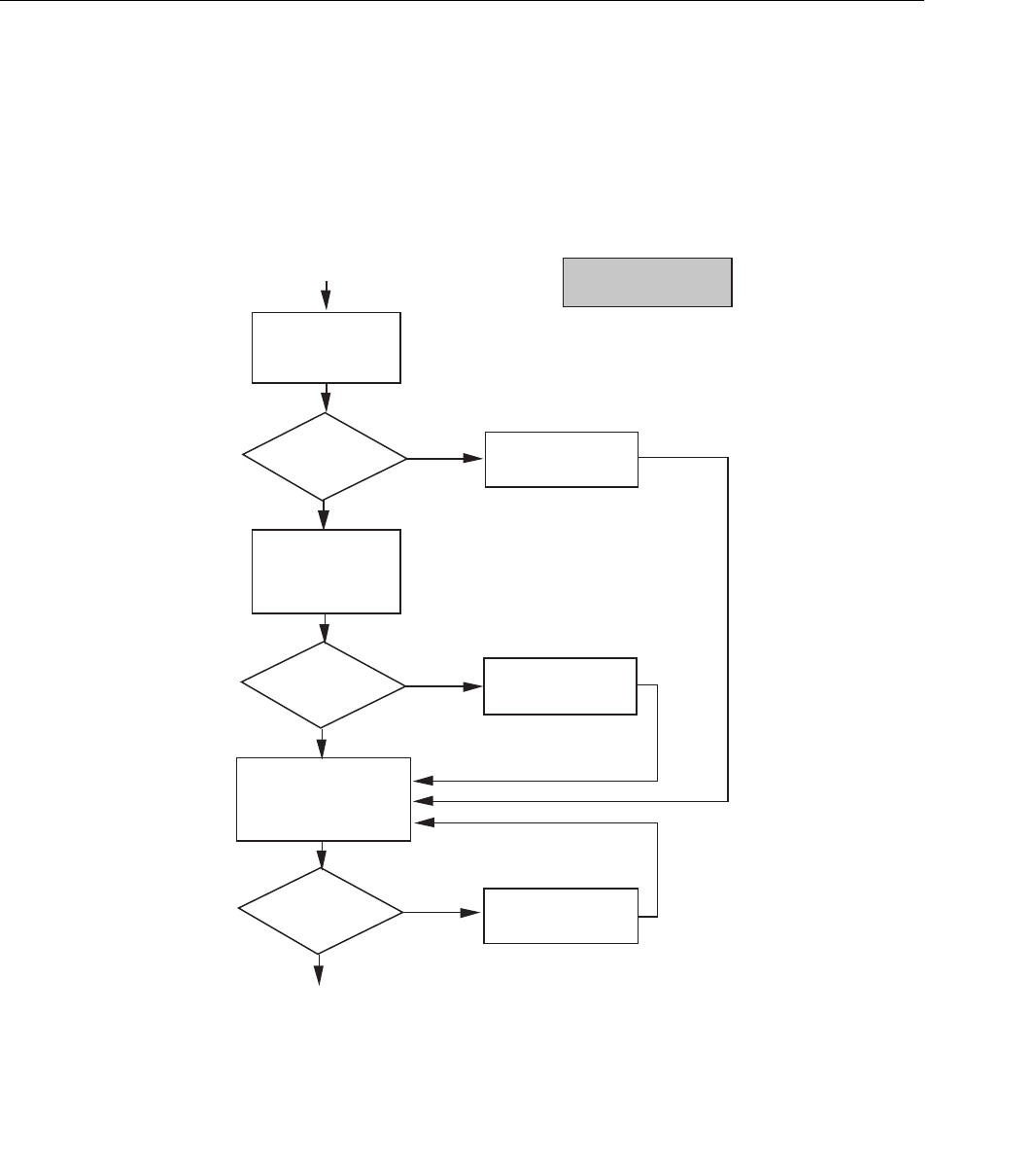
9-4
68P81095E02-D 12/12/2000
800/900/1500 MHz Base Radios EBTS System Manual - Vol 2
Reported/Suspected Problem
Use Procedure 2 to troubleshoot reported or suspected equipment malfunctions.
Perform this procedure with equipment in service (non-intrusive) and with
equipment taken temporarily out of service (intrusive).
Figure 9-2 shows the Procedure 2 Troubleshooting Flowchart.
Figure:9-2
Procedure 2 Troubleshooting Flowchart
PROCEDURE 2
PROBLEM
REPORTED OR SUSPECTED
DONE
Clear Problem Report
OBSERVE LED
INDICATORS
Module Suspected
of Being Faulty?
Ye s Go to Module Replacement
Procedures Section
No
CHECK CURRENT
ALARM STATUS
Use MMI command
get alarms
to check alarm status
Module Suspected
of Being Faulty? Go to Module Replacement
Procedures Section
PERFORM
VERIFICATION TESTS
Use MMI commands to
perform tests as specified in
station verification procedure.
Module Suspected
of Being Faulty? Go to Module Replacement
Procedures Section
Ye s
No
Ye s
No
Refer to
Controls and Indicators
for LED Definitions
EBTS022
071895JNM

68P81095E02-D 12/12/2000
9
-
5
EBTS System Manual - Vol 2 800/900/1500 MHz Base Radios
Base Radio/Base Radio FRU Replacement Procedures
Base Radio/Base Radio FRU
Replacement Procedures
Replace suspected station modules with known non-defective modules to restore
the station to proper operation. The following procedures provide FRU
replacement instructions, post-replacement adjustments and veriÞcation
instructions.
Base Radio Replacement Procedure
NOTE
Base Radio removal and installation procedures
appear for reference or buildout purposes. Field
maintenance of Base Radios typically consists of
replacement of FRUs within the Base Radio. Perform
Base Radio FRU replacement according to ÒBase Radio
FRU Replacement ProcedureÓ below.
Perform Base Radio (BR) replacement as described in the following paragraphs.
CAUTION
!
Improper lifting or dropping the BR could result in
serious personal injury or equipment damage.
Base Radios are HEAVY!
Handle the BR with extreme caution, and according to
local health and safety regulations.
Removal
Remove the BR from the Equipment Cabinet as follows:
CAUTION
!
A Single Carrier BR can weigh up to 76 LBS (34 KG). A
Quad Carrier BR can weigh up to 91 LBS (41 KG).
Handle the BR with extreme caution, and according to
local health and safety regulations.

9-6
68P81095E02-D 12/12/2000
800/900/1500 MHz Base Radios EBTS System Manual - Vol 2
Base Radio/Base Radio FRU Replacement Procedures
1.
Remove power from the Base Radio by setting the Power Supply ON/OFF
switch to the OFF position.
2.
Tag and disconnect the cabling from the BR rear panel connectors.
3.
Remove the Power AmpliÞer module to reduce the BR weight. Remove the
two M10 Torx screws that secure the Power AmpliÞer module. Slide the
module out of the chassis.
4.
Remove the four M30 TORX screws which secure the BR front panel to the
Equipment Cabinet mounting rails.
5.
While supporting the BR, carefully remove the BR from the Equipment
Cabinet by sliding the BR from the front of cabinet.
When the BR becomes free
from its mounting rails, be sure to fully support it.
Installation
Install BR in Equipment Cabinet as follows:
CAUTION
!
A Single Carrier BR can weigh up to 76 LBS (34 KG). A
Quad Carrier BR can weigh up to 91 LBS (41 KG).
Handle the BR with extreme caution, and according to
local health and safety regulations.
1.
If adding a BR, install side rails in the appropriate BR mounting position in
the rack.
2.
Remove the Power AmpliÞer module to reduce the BR weight. Remove the
two M10 Torx screws that secure the Power AmpliÞer module. Slide the
module out of the chassis.
3.
While supporting the BR, carefully lift and slide the BR in the Equipment
Cabinet mounting position.
4.
Secure the BR to the Equipment Cabinet mounting rails using four M30 Torx
screws. Tighten the screws to 40 in-lb (4.5 Nm).
5.
Slide the Power AmpliÞer module back into the BR chassis. Replace two
M10 Torx screws that secure the Power AmpliÞer module. Secure the
module by tightening the screws to the speciÞed torque of 5 in-lbs.
6.
Connect the cabinet cabling to the BR. Refer to Backplane Þgure XX.
7.
Perform BR activation as decribed below.

68P81095E02-D 12/12/2000
9
-
7
EBTS System Manual - Vol 2 800/900/1500 MHz Base Radios
Base Radio/Base Radio FRU Replacement Procedures
NOTE
Base Radio removal and installation procedures
appear for reference or buildout purposes. Field
maintenance of Base Radios typically consists of
replacement of FRUs within the Base Radio. Perform
Base Radio FRU replacement according to ÒBase Radio
FRU Replacement ProcedureÓ below.
Anti-Static Precautions
CAUTION
The Base Radio contains static-sensitive devices.
Prevent electrostatic discharge damage to Base Radio
modules! When replacing Base Radio FRUs, wear a
grounded wrist strap. Observe proper anti-static
procedures.
Motorola publication 68P81106E84 provides complete static protection
information. This publication is available through Motorola National Parts.
Observe the following additional precautions:
❐
Wear a wrist strap (Motorola Part No. 4280385A59 or equivalent) at all times
when servicing the Base Radio to minimize static build-up.
❐
A grounding clip is provided with each EBTS cabinet. If not available, use
another appropriate grounding point.
❐
DO NOT insert or remove modules with power applied to the Base Radio.
ALWAYS turn the power OFF using the Power Supply rocker switch on the
front of the Power Supply module.
❐
Keep spare modules in factory packaging for transporting. When shipping
modules, always pack in original packaging.
FRU Replacement Procedure
Perform the following steps to replace any of the Base Radio FRUs:

9-8
68P81095E02-D 12/12/2000
800/900/1500 MHz Base Radios EBTS System Manual - Vol 2
Base Radio/Base Radio FRU Replacement Procedures
NOTE
After a Control Board or BR replacement, the
integrated Site Controller (iSC) reboots the BR.
Whenever the BR goes off-line, the Replacement BRC
Accept Timer begins counting down. A BR reboot
occurs if the BR remains off-line as the timer times out.
(The timerÕs default period is three minutes.) If
someone turns on the BR before the timer times out,
power down the BR. Then wait for the minimum
timer period before turning on the BR.
1.
Notice the Power Supply rocker switch, behind the front panel of the Power
Supply. Set the Power Supply rocker switch to the OFF (0) position. Turning
off this switch removes power from the Base Radio.
2.
Loosen the front panel fasteners. These are located on each side of the
module being replaced.
3.
Pull out the module.
4.
Insert the non-defective replacement module by aligning the module side
rails with the appropriate rail guides inside the Base Radio chassis.
5.
Gently push the replacement module completely into the Base Radio chassis
assembly using the module handle(s).
CAUTION
DO NOT slam or force the module into the chassis
assembly. Rough handling can damage the connectors
or backplane.
6.
Secure the replacement module by tightening the front panel fasteners to the
speciÞed torque of 5 in-lbs.
7.
Apply power to the Base Radio by setting the switch to the ON position.
8.
Perform the Station VeriÞcation Procedure.

68P81095E02-D 12/12/2000
9
-
9
EBTS System Manual - Vol 2 800/900/1500 MHz Base Radios
Base Radio/Base Radio FRU Replacement Procedures
Power Amplifier (PA) Fan FRU Replacement
Perform the following steps to replace the Power AmpliÞer (PA) fans.
1.
Remove the Power AmpliÞer from the Base Radio per FRU Replacement
Procedure.
2.
Disconnect fan power cable from PA housing.
3.
Remove front panel from fan assembly.
4.
Remove fan assembly from PA chassis.
NOTE
To install the new fan kit, reverse above procedure.

9-10
68P81095E02-D 12/12/2000
800/900/1500 MHz Base Radios EBTS System Manual - Vol 2
Station Verification Procedures
Station Verification Procedures
Perform the Station VeriÞcation Procedures whenever you replace a FRU. The
procedures verify transmit and receive operations. Each procedure also contains
the equipment setup.
Replacement FRU Verification
Before shipment, the factory programs all module-speciÞc information. Base
Radio speciÞc information (e.g., receive and transmit frequencies) involves a
download to the Base Radio from the network/site controller.
The Base Radio does not require replacement FRU alignment.
Base Repeater FRU Hardware Revision Verification
NOTE
The following procedure requires the Base Radio to be
out of service. Unless the Base Radio is currently out
of service, Motorola recommends performing this
procedure during off-peak hours. Performing this
procedure then minimizes or eliminates disruption of
service to system users.
1.
Connect one end of the RS-232 cable to the service computer.
2.
Connect the other end of the RS-232 cable to the STATUS port, located on the
front panel of the EX/CNTL module.
3.
Power on the BR using the front switch on the Power Supply Module. Press
the reset button on the Control Module front panel. At the prompt, hit a
Carriage Return on the service computer to enter the test application mode.
Using the password
Motorola
, log in to the BR.
:> login -ufield
password: *****
field>motorola
field>

68P81095E02-D 12/12/2000
9
-
11
EBTS System Manual - Vol 2 800/900/1500 MHz Base Radios
Station Verification Procedures
4.
Collect revision numbers from the station by typing the
following command:
5.
If all modules return revision numbers of the format ÒRxx.xx.xxÓ, then all
revision numbers are present. In that case, veriÞcation requires no further
action. If revision numbers return as blank, or not in the format ÒRxx.xx.xxÓ,
contact your local Motorola representative or Technical Support.
6.
Set desired cabinet id and position and of BR by typing the following
commands with the Þnal number on each command being the desired
cabinet id and position. The command example below sets cabinet id to 5,
and cabinet position to 2.
7.
After checking all BRs, log out by keying the following command:
Transmitter Verification
The transmitter veriÞcation procedure veriÞes transmitter operation and transmit
path integrity. Motorola recommends this veriÞcation procedure after replacing
an Exciter, Power AmpliÞer, BRC, or Power Supply module.
field> fv -oplatform
field>
field> ci -oplatform -c5
field> pi -oplatform -p2
field>
field> logout
field>

9-12 68P81095E02-D 12/12/2000
800/900/1500 MHz Base Radios EBTS System Manual - Vol 2
Station Verification Procedures
NOTE
The following procedure requires the Base Radio to be
out of service. Unless the Base Radio is currently out
of service, Motorola recommends performing this
procedure during off-peak hours. Performing this
procedure then minimizes or eliminates disruption of
service to system users.
Equipment Setup
To set up the equipment, use the following procedure:
1. Remove power from the Base Radio by setting the Power Supply rocker
switch (located behind the front panel of the Power Supply) to the OFF (0)
position.
2. Connect one end of the RS-232 cable to the service computer.
3. Connect the other end of the RS-232 cable to the STATUS port located on the
front panel of the BRC.
4. Disconnect the existing cable from the connector labeled PA OUT. This
connector is located on the backplane of the Base Radio.
5. Connect a test cable to the PA OUT connector.
6. Connect a 10 dB attenuator on the other end of the test cable.
7. From the attenuator, connect a cable to the RF IN/OUT connector on the
R2660 Communications Analyzer.
8. Remove power from the R2660. Connect the Rubidium Frequency Standard
10MHZ OUTPUT to a 10 dB attenuator.
9. Connect the other end of the 10 dB attenuator to the 10MHZ REFERENCE
OSCILLATOR IN/OUT connector on the R2660.
NOTE
Refer to the R2660 equipment manual for further
information regarding mode conÞguration of the unit.
(Motorola Part No. 68P80386B72.)
10. Set the R2660 to the EXT REF mode.
11. Apply power to the R2660.
12. Set the R2660 to the SPECTRUM ANALYZER mode with the center
frequency set to the transmit frequency of the Base Radio under test.

68P81095E02-D 12/12/2000 9-13
EBTS System Manual - Vol 2 800/900/1500 MHz Base Radios
Station Verification Procedures
13. Perform the appropriate transmitter veriÞcation procedure below for the
particular Power AmpliÞer used in the Base Radio.
Transmitter Verification Procedure
(QUAD Carrier 800 MHz Power Amplifiers)
This procedure provides commands and responses to verify proper operation of
the transmit path for 800 MHz Base Radios using a 70 Watt Power AmpliÞer.
1. Power on the BR using the front switch on the Power Supply Module. Press
the reset button on the Control Module front panel. At the prompt, hit a
Carriage Return on the service computer to enter the test application mode.
Using the password Motorola, login to the BR.
2. Dekey the BR to verify that no RF power is being transmitted. Set the
transmit DSP test mode to Òstop.Ó At the Þeld> prompt, type:
CAUTION
!
The following command keys the transmitter. Make
sure that transmission only occurs on licensed
frequencies, or into an RF dummy load.
3. Key the BR to 40 watts, following the steps below from the Þeld> prompt :
3.1 Set the frequency of transmit channel 1 through 4.
:> login -ufield
password: *****
field>motorola
field>
field> ptm -otx_all -mstop
field> power -otxch1 -p0
field>

9-14 68P81095E02-D 12/12/2000
800/900/1500 MHz Base Radios EBTS System Manual - Vol 2
Station Verification Procedures
3.2 Set the transmit DSP test mode to Òdnlk_framed.Ó
3.3 Enable the channels by setting a data pattern to Òiden.Ó
3.4 Set the transmit power to 40 watts and key the BR.
4. After keying the Base Radio, verify the stationÕs forward and reßected
power and VSWR. Check these Þgures against the parameters in Table 9-2.
Table 9-2
QUAD BRTransmitter Parameters
Parameter Value or Range
Forward Power Greater than 36 Watts
Reßected Power Less than 2.0 Watts
VSWR Less than 1.6:1
field> freq -otxch1 -f860
field> freq -otxch2 -f860.025
field> freq -otxch3 -f860.05
field> freq -otxch4 -f860.075
field>
field> ptm -otx_all -mdnlk_framed
field>
field> dpm -otxch1 -miden
field> dpm -otxch2 -miden
field> dpm -otxch3 -miden
field> dpm -otxch4 -miden
field>
field> power -otxch1 -p40
field>

68P81095E02-D 12/12/2000 9-15
EBTS System Manual - Vol 2 800/900/1500 MHz Base Radios
Station Verification Procedures
4.1 Check channel 1. At the Þeld> prompt, type:
4.2 Check channel 2. At the Þeld> prompt, type:
4.3 Check channel 3. At the Þeld> prompt, type:
4.4 Check channel 4. At the Þeld> prompt, type:
5. This command returns all active alarms of the Base Radio. At the Þeld>
prompt, type:
NOTE
If the alarms command displays alarms, refer to the
System Troubleshooting chapter for corrective actions.
6. View the spectrum of the transmitted signal on the R2660 Communications
Analyzer. Use the Spectrum Analyzer mode. Figure 9-3 shows a sample of
the spectrum.
field> power -otxch1
field>
field> power -otxch2
field>
field> power -otxch3
field>
field> power -otxch4
field>
field> alarms -ofault_hndlr
field>
9-16 68P81095E02-D 12/12/2000
800/900/1500 MHz Base Radios EBTS System Manual - Vol 2
Station Verification Procedures
7. Dekey the BR to verify that no RF power is being transmitted. Set the
transmit DSP test mode to Òstop." At the Þeld> prompt, type:
Equipment Disconnection
Use the following steps to disconnect equipment after verifying the transmitter.
1. Remove power from the Base Radio by setting the Power Supply rocker
switch (located behind the front panel of the Power Supply) to the OFF (0)
position.
2. Disconnect the RS-232 cable from the connector on the service computer.
3. Disconnect the other end of the RS-232 cable from the RS-232 connector
located on the front panel of the BRC.
Figure:9-3
Quad Channel Spectrum (800 MHz BR)
field> ptm -otx_all -mstop
field> power -otxch1 -p0
field>

68P81095E02-D 12/12/2000 9-17
EBTS System Manual - Vol 2 800/900/1500 MHz Base Radios
Station Verification Procedures
4. Disconnect the test cable from the PA OUT connector located on the
backplane of the Base Radio.
5. Connect the standard equipment cable to the PA OUT connector.
6. Disconnect the 10 dB attenuator from the other end of the test cable.
7. From the attenuator, disconnect the cable to the R2660
Communications Analyzer.
8. Restore power to the Base Radio by setting the Power Supply rocker switch
to the ON (1) position.
9. If necessary, continue with the Receiver VeriÞcation Procedure.
Receiver Verification
The receiver veriÞcation procedure sends a known test signal into the Base Radio
to verify the receive path. This veriÞcation procedure is recommended after
replacing a Receiver.
NOTE
The following procedure requires the Base Radio to be
out of service. Unless the base radio is currently out of
service, Motorola recommends performing this
procedure during off-peak hours. Performing this
procedure then minimizes or eliminates disruption of
services to system users.
Equipment Setup
Set up equipment for the receiver veriÞcation procedure as follows:
1. Remove power from the Base Radio by setting the Power Supply rocker
switch (located behind the front panel of the Power Supply) to the OFF (0)
position.
2. Connect one end of the RS-232 cable to the service computer.
3. Connect the other end of the RS-232 cable to the STATUS port located on the
front panel of the BRC.
4. Disconnect the existing cable from the connector labeled RX1 (or the
connector corresponding to the receiver under test). Connector RX1 is on the
Base Radio backplane.
5. Connect a test cable to the RX 1 connector.
6. Use an HP4432b to measure BR performance

9-18 68P81095E02-D 12/12/2000
800/900/1500 MHz Base Radios EBTS System Manual - Vol 2
Station Verification Procedures
7. Attach RF output from the HP4432b to a 3 way splitter. Attach the output of
the three way splitter to the antenna connections in the back of the BR.
8. Attach the 'event 2' port in the rear panel to pin 6 on the front panel of the
BR.
9. The 4432b must have the Proprietary Tornado downlink Þles to be
conÞgured correctly.
10. Turn on the 4432b. Press the 'mode' key. Select the 'arbitrary waveform
generator'. Select 'Dual Arb'. Goto 'waveform select' and choose Tornado.
Choose 'waveform segments'. Select the 'load' softkey. Choose the softkey
'Store all To NVARB Memory'. Press the 'return' softkey.
11. Select 'ARB setup' and set the sample clock to 100khz.
12. Attach the TFR 5Mhz to the 'Gen ref in'.
13. Set the reference frequency to the correct frequency (5Mhz) and select 'ARB
Reference' EXT for external reference.
14. Select the I/Q key. Goto the next page by selecting 'More (1 of 2)'. Turn 'ALC'
off by selecting the softkey.
15. Select the 'Mode' key again, followed by the 'arbitrary waveform generator'
softkey, 'Dual Arb'
16. Set the frequency and power out and turn on the modulation and RF out.
Receiver Verification Procedure
This procedure provides commands and responses to verify proper operation of
Base Radio receiver paths. Perform the procedure on all four receivers in the BR.
1. Power on the BR using the front switch on the Power Supply Module. Press
the reset button on the Control Module front panel. At the prompt, hit a
Carriage Return on the service computer to enter the test application mode.
Using the password Motorola, login to the BR..
2. ConÞgure the arbitrary waveform generator (ARB) and Vector Signal
Generator A to generate the desired Q-QAM test signal in a 3RX mode at the
desired frequency. The RF Power Out of Vector Signal Generator A should
be set to -108 dBm
>login –ufield
>password: *****
field>motorola
field>

68P81095E02-D 12/12/2000 9-19
EBTS System Manual - Vol 2 800/900/1500 MHz Base Radios
Station Verification Procedures
3. Using the MMI commands below, issue the command to put the BR into
3RX mode. If the resulting bit error rates for receiver branches 1, 2, and 3 are
less than 8%, the receiver has passed the test.
3.1 Start by checking Receiver 1. At the Þeld> prompt, type:
3.2 Check Receiver 2. At the Þeld> prompt, type:
3.3 Check Receiver 3. At the Þeld> prompt, type:
field> freq -orxch1 -f810
field> enable -orxch1 -son
field> sge -orx_all -soff
field> es -orx_all -text_trigger
field> peer_performance_config -orxch1 -mpath -pall
field> peer_performance_report -orxch1 -a100 -r1
field>
field> freq -orxch2 -f810
field> enable -orxch2 -son
field> sge -orx_all -soff
field> es -orx_all -text_trigger
field> peer_performance_config -orxch2 -mpath -pall
field> peer_performance_report -orxch2 -a100 -r1
field>
field> freq -orxch3 -f810
field> enable -orxch3 -son
field> sge -orx_all -soff
field> es -orx_all -text_trigger
field> peer_performance_config -orxch3 -mpath -pall
field> peer_performance_report -orxch3 -a100 -r1
field>

9-20 68P81095E02-D 12/12/2000
800/900/1500 MHz Base Radios EBTS System Manual - Vol 2
Station Verification Procedures
3.4 Check Receiver 4. At the Þeld> prompt, type:
4. Enter the command to return all active alarms of the Base Radio. At the
Þeld> prompt, type:
NOTE
If the command displays alarms, refer to the System
Troubleshooting section for corrective actions.
5. As an option, you may check kit numbers for the receiver and other
modules. The following command returns this data. (The example below
speciÞes 800 MHz Quad Base Radios.) At the Þeld> prompt, type:
Equipment Disconnection
After verifying receiver operation, disconnect equipment as follows:
1. Notice the Power Supply rocker switch, behind the front panel of the Power
Supply. Set the Power Supply rocker switch to the OFF (0) position. Turning
off this switch removes power from the Base Radio.
2. Disconnect the RS-232 cable from the connector on the service computer.
field> freq -orxch4 -f810
field> enable -orxch4 -son
field> sge -orx_all -soff
field> es -orx_all -text_trigger
field> peer_performance_config -orxch4 -mpath -pall
field> peer_performance_report -orxch4 -a100 -r1
field>
field> alarms_ofault_hndlr
field>
field> fv -oplatform
field>

68P81095E02-D 12/12/2000 9-21
EBTS System Manual - Vol 2 800/900/1500 MHz Base Radios
Station Verification Procedures
3. Disconnect the other end of the RS-232 cable from the RS-232 connector on
the front panel of the BRC.
4. Disconnect the test cable from the RX1, RX2, and RX3 connectors located on
the backplane of the Base Radio.
5. Connect the standard equipment cable to the RX1 connector.
6. Restore power to the Base Radio by setting the Power Supply rocker switch
to the ON (1) position. This step completes the Receiver VeriÞcation
Procedure for the receiver under test.
7. Repeat the Receiver VeriÞcation Procedure for each Quad receiver in every
Base Radio in the EBTS.

9-22 68P81095E02-D 12/12/2000
800/900/1500 MHz Base Radios EBTS System Manual - Vol 2
QUAD Channel BR Backplane
QUAD Channel BR Backplane
Backplane Connectors
The Base Radio backplane includes all external equipment connections. Table 9-3
lists and describes the backplane connectors.
Table 9-3
Backplane Connectors
Connector Module Description Connector Type
P1 EXBRC Signal 168 Pin AMP Z-Pack
Futurebus
P2 RX1 Signal 72 Pin AMP Z-Pack
Futurebus
P3 RX1 RF 6 coax Harting Harpak
P4 RX2 Signal 72 Pin AMP Z-Pack
Futurebus
P5 RX2 RF 6 coax Harting Harpak
P6 RX3 Signal 72 Pin AMP Z-Pack
Futurebus
P7 RX3 RF 6 coax Harting Harpak
P8 RX4 Signal 72 Pin AMP Z-Pack
Futurebus
P9 RX4 RF 6 coax Harting Harpak
P10 PA Signal 96 Pin EURO
P11 PS Signal & Power 78 Pin AMP Teledensity
P12a
a. P12 is a cutout in the backplane with threaded inserts for securing the connector which
mates directly to the power supply.
PS -48 Vdc Power In 8 Pin AMP 530521-3
P13 EX RF(EX from PA) SMA blindmate
P14 EX RF(EX to PA) SMA blindmate
P15 External / EXBRC Ethernet BNC blindmate
P16 External / PA RF (PA from EX) SMA blindmate
P17 External / PA RF (PA to EX) SMA Blindmate
P18 External / PA TX Output SMA blindmate
P19 RX Branch 1 RF SMA
P20 RX Branch 2 RF SMA
P21 RX Branch 3 RF SMA
P22b
b. P22 will not be placed on the Tornado backplane. However, the backplane shall be
designed with P22 to allow for reuse on other products.
External RS232 Dsub-9
P23 External Alarm Dsub-25
P24 External 5MHz/1PPS BNC
68P81095E02-D 12/12/2000 9-23
EBTS System Manual - Vol 2 800/900/1500 MHz Base Radios
QUAD Channel BR Backplane
Figure 9-4 shows the locations of the Base Radio external connections.
Backplane RF Connections
When the factory ships Base Radios as FRUs, each connection on the back of a
repeater has a designated color dot beside it. See Table 9-4. To Þnd where a cable
should be connected, match the label wrapped around the cable to the dot on the
back of the repeater.
Table: 9-4
Color Codes for RF Connections on Rear of Base Radio
Connectors Color Dot Code
TX Orange
RX 1 Red
RX 2 Green
RX 3 Yellow
Ethernet White
5 MHz/1 pps A
or Spare
Gray
EX OUT
PA IN
EX
PA FB
DC POWER
AC POWER
RS 232ALARM
5MHZ/1 PPS B
RX 1
RX 2
RX 3
5MHZ/1 PPS A
ETHERNET A
PA OUT
GROUND
EBTS327
021997JNM
RE BLACK
This port must be terminated by 50Ω load when configured for
2 Branch Diversity. Also, the rx_fru_config parameter must be set to R12.
*
*
Figure:9-4
Base Radio Backplane Connectors
T
HIS
P
ICTURE
MUST
BE
CHANGED
!

9-24 68P81095E02-D 12/12/2000
800/900/1500 MHz Base Radios EBTS System Manual - Vol 2
QUAD Channel BR Backplane
Backplane Connector Pinouts
Table 9-5 lists the pin-outs for the Base Radio Controller boardÕs 168-pin P1
connector.
Table: 9-5
EXBRC P1 Pinout, Signal and Power
Row ABCD
1 GND 3.3 Vdc 3.3 Vdc NC
2 GND 3.3 Vdc 14.2 Vdc 14.2 Vdc
3 GND 3.3 Vdc 14.2 Vdc 14.2 Vdc
4 GND GND GND GND
5NCNCNCNC
6 GND GND GND GND
7 GND 16.8MHz_RX 16.8MHz_RX_RTN GND
8 GND GND GND GND
9 GND 5 MHz/1 PPS 3.3 Vdc 3.3 Vdc
10 NC NC NC 3.3 Vdc
11 TxD CTS DTR BRG
12 RTS RxD DSR CD
13 NC NC NC 3.3 Vdc
14 NC NC SHUTDOWN_ SLEEP_
15 PA_ENABLE NC 28.6 Vdc 14.2 Vdc
16 NC NC NC 3.3 Vdc
17 EXT_GPI_1_ EXT_GPI_2_ EXT_GPO_1_ EXT_GPO_2_
18 BAT_STAT_ MTR_STAT_ EXT_VFWD EXT_VREV
19 SPI_M3 SPI_M2 SPI_M1 SPI_M0
20 SPI_ENABLE SPI_MOSI SPI_MISO SPI_CLK
21 SPI_A2 SPI_A1 SPI_A0 WP_
22 NC RxRESET_ NC NC
23 NC Clock_SyncB_ NC NC
24 GND GND 3.3 Vdc 3.3 Vdc
25 SSI_Data_D SSI_CLK_D SSI_FS_D 3.3 Vdc
26 SSI_Data_D_RTN SSI_CLK_D_RTN NC 3.3 Vdc
27 GND GND 3.3 Vdc 3.3 Vdc
28 DSPIb_MOSI DSPIb_CLK DSPIb_EN_1 DSPIb_EN_2
29 DSPIb_MOSI_RTN DSPIb_CLK_RTN DSPIb_EN_3 NC
30 GND GND 3.3 Vdc 3.3 Vdc
31 GND SSI_Data_C SSI_CLK_C SSI_FS_C
32 GND SSI_Data_C_RTN SSI_CLK_C_RTN NC
33 NC Clock_SyncA_ NC NC
34 GND GND 3.3 Vdc 3.3 Vdc
35 SSI_Data_B SSI_CLK_B SSI_FS_B 3.3 Vdc

68P81095E02-D 12/12/2000 9-25
EBTS System Manual - Vol 2 800/900/1500 MHz Base Radios
QUAD Channel BR Backplane
36 SSI_Data_B_RTN SSI_CLK_B_RTN NC 3.3 Vdc
37 GND GND 3.3 Vdc 3.3 Vdc
38 DSPIa_MOSI DSPIa_CLK DSPIa_EN_1 DSPIa_EN_2
39 DSPIa_MOSI_RTN DSPIa_CLK_RTN DSPIa_EN_3 NC
40 GND GND 3.3 Vdc 3.3 Vdc
41 GND SSI_Data_A SSI_CLK_A SSI_FS_A
42 GND SSI_Data_A_RTN SSI_CLK_A_RTN NC
Table: 9-6
EXBRC P13 Pinout, Exciter from PA
Coaxial Description
Center PA IN
Outer GND
Table: 9-7
EXBRC P14 Pinout, Exciter to PA
Coaxial Description
Center PA Feedback
Outer GND
Table: 9-8
EXBRC P15 Pinout, Ethernet
Coaxial Description
Center Ethernet
Outer GND
Table: 9-5
EXBRC P1 Pinout, Signal and Power
Row ABCD

9-26 68P81095E02-D 12/12/2000
800/900/1500 MHz Base Radios EBTS System Manual - Vol 2
QUAD Channel BR Backplane
RX1 Connections
Table 9-9
RX1 P2 Pinout, Signal and Power
Row A B C D
1 NC GND GND Clock_SyncA_
2 GND DSPIa_MOSI_RTN DSPIa_CLK_RTN DSPIa_EN_1
3 GND DSPIa_MOSI DSPIa_CLK DSPIa_EN_2
4 GND GND GND GND
5 14.2 SSI_CLK_A_RTN SSI_FS_B SSI_CLK_B_RTN
6 14.2 SSI_CLK_A SSI_FS_A SSI_CLK_B
7 14.2 GND GND GND
8 14.2 SSI_Data_A_RTN GND SSI_Data_B
9 GND SSI_Data_A GND SSI_Data_B_RTN
10 GND NC NC NC
11 3.3 RxRESET_ GND (ID0) GND (ID1)
12 3.3 WP_ SPI_A0 SPI_A1
13 3.3 SPI_MISO SPI_CLK SPI_A2
14 GND SPI_M0 SPI_ENABLE SPI_MOSI
15 GND SPI_M1 SPI_M2 SPI_M3
16 GND GND GND NC
17 GND 16.8MHz_RX GND NC (WB switch)
18 GND 16.8MHz_RX_RTN GND NC (MC switch)
Table 9-10
RX1 P3 Pinout, RF Input and Output Connection
Row A B C D E
1 GND - GND - GND
2 - RX3_EXP3 - RX1_EXP3 -
3 GND - GND - GND
4 GND - GND - GND
5 - RX2_EXP2 - RX1_EXP2 -
6 GND - GND - GND
7 GND - GND - GND
8 - RX Branch 1 - RX1_EXP1 -
9 GND - GND - GND

68P81095E02-D 12/12/2000 9-27
EBTS System Manual - Vol 2 800/900/1500 MHz Base Radios
QUAD Channel BR Backplane
RX2 Connections
Table 9-11
RX2 P4 Pinout, Signal and Power
Row A B C D
1 NC GND GND Clock_SyncA_
2 GND DSPIa_MOSI_RTN DSPIa_CLK_RTN DSPIa_EN_3
3 GND DSPIa_MOSI DSPIa_CLK DSPIa_EN_2
4 GND GND GND GND
5 14.2 SSI_CLK_B_RTN NC NC
6 14.2 SSI_CLK_B SSI_FS_B NC
7 14.2 GND GND GND
8 14.2 SSI_Data_B_RTN GND NC
9 GND SSI_Data_B GND NC
10 GND NC NC NC
11 3.3 RxRESET_ NC (ID0) GND (ID1)
12 3.3 WP_ SPI_A0 SPI_A1
13 3.3 SPI_MISO SPI_CLK SPI_A2
14 GND SPI_M0 SPI_ENABLE SPI_MOSI
15 GND SPI_M2 SPI_M1 SPI_M3
16 GND GND GND NC
17 GND 16.8MHz_RX GND NC (WB switch)
18 GND 16.8MHz_RX_RTN GND NC (MC switch)
Table 9-12
RX2 P5 Pinout, RF Input and Output Connection
Row A B C D E
1 GND - GND - GND
2 - RX3_EXP2 - RX2_EXP3 -
3 GND - GND - GND
4 GND - GND - GND
5 - RX1_EXP1 - RX2_EXP2 -
6 GND - GND - GND
7 GND - GND - GND
8 - RX Branch 2 - RX2_EXP1 -
9 GND - GND - GND

9-28 68P81095E02-D 12/12/2000
800/900/1500 MHz Base Radios EBTS System Manual - Vol 2
QUAD Channel BR Backplane
RX3 Connections
Table 9-13
RX3 P6 Pinout, Signal and Power
Row A B C D
1 NC GND GND Clock_SyncB_
2 GND DSPIb_MOSI_RTN DSPIb_CLK_RTN DSPIb_EN_1
3 GND DSPIb_MOSI DSPIb_CLK DSPIb_EN_2
4 GND GND GND GND
5 14.2 SSI_CLK_C_RTN SSI_FS_D SSI_CLK_D_RTN
6 14.2 SSI_CLK_C SSI_FS_C SSI_CLK_D
7 14.2 GND GND GND
8 14.2 SSI_Data_C_RTN GND SSI_Data_D
9 GND SSI_Data_C GND SSI_Data_D_RTN
10 GND NC NC NC
11 3.3 RxRESET_ GND (ID0) NC (ID1)
12 3.3 WP_ SPI_A0 SPI_A1
13 3.3 SPI_MISO SPI_CLK SPI_A2
14 GND SPI_M2 SPI_ENABLE SPI_MOSI
15 GND SPI_M1 SPI_M0 SPI_M3
16 GND GND GND NC
17 GND 16.8MHz_RX GND GND (WB switch)
18 GND 16.8MHz_RX_RTN GND NC (MC switch)
Table 9-14
RX3 P7 Pinout, RF Input and Output Connection
Row A B C D E
1 GND - GND - GND
2 - RX1_EXP2 - RX3_EXP3 -
3 GND - GND - GND
4 GND - GND - GND
5 - RX2_EXP1 - RX3_EXP2 -
6 GND - GND - GND
7 GND - GND - GND
8 - RX Branch 3 - RX3_EXP1 -
9 GND - GND - GND

68P81095E02-D 12/12/2000 9-29
EBTS System Manual - Vol 2 800/900/1500 MHz Base Radios
QUAD Channel BR Backplane
RX4 Connections
Table 9-15
RX4 P8 Pinout, Signal and Power
Row A B C D
1 NC GND GND Clock_SyncB_
2 GND DSPIb_MOSI_RTN DSPIb_CLK_RTN DSPIb_EN_3
3 GND DSPIb_MOSI DSPIb_CLK DSPIb_EN_2
4 GND GND GND GND
5 14.2 SSI_CLK_D_RTN NC NC
6 14.2 SSI_CLK_D SSI_FS_D NC
7 14.2 GND GND GND
8 14.2 SSI_Data_D_RTN GND NC
9 GND SSI_Data_D GND NC
10 GND NC NC NC
11 3.3 RxRESET_ NC (ID0) NC (ID1)
12 3.3 WP_ SPI_A0 SPI_A1
13 3.3 SPI_MISO SPI_CLK SPI_A2
14 GND SPI_M0 SPI_ENABLE SPI_MOSI
15 GND SPI_M3 SPI_M2 SPI_M1
16 GND GND GND NC
17 GND 16.8MHz_RX GND NC (WB switch)
18 GND 16.8MHz_RX_RTN GND GND (MC switch)
Table 9-16
RX4 P9 Pinout, RF Input and Output Connection
Row A B C D E
1 GND - GND - GND
2 - RX1_EXP3 - NC -
3 GND - GND - GND
4 GND - GND - GND
5 - RX2_EXP3 - NC -
6 GND - GND - GND
7 GND - GND - GND
8 - RX3_EXP1 - NC -
9 GND - GND - GND

9-30 68P81095E02-D 12/12/2000
800/900/1500 MHz Base Radios EBTS System Manual - Vol 2
QUAD Channel BR Backplane
PA Connections
Table 9-17
PA P10 Pinout, Signal and Power
Row A B C
1 SPI_ENABLE GND 28.6 Vdc
2 GND GND 28.6 Vdc
3 SPI_A0 GND 28.6 Vdc
4 GND GND 28.6 Vdc
5 SPI_A1 GND 28.6 Vdc
6 GND GND 28.6 Vdc
7 SPI_A2 GND 28.6 Vdc
8 GND GND 28.6 Vdc
9 SPI_M0 GND 28.6 Vdc
10 GND GND 28.6 Vdc
11 SPI_M1 GND 28.6 Vdc
12 GND GND 28.6 Vdc
13 SPI_M2 GND 28.6 Vdc
14 GND GND 28.6 Vdc
15 SPI_M3 GND 28.6 Vdc
16 GND GND 28.6 Vdc
17 SPI_MISO GND 28.6 Vdc
18 GND GND 28.6 Vdc
19 SPI_MOSI GND 28.6 Vdc
20 GND GND 28.6 Vdc
21 SPI_CLK GND 28.6 Vdc
22 GND 3.3 Vdc 28.6 Vdc
23 WP* 3.3 Vdc 28.6 Vdc
24 GND GND 28.6 Vdc
25 PA_ENABLE GND 28.6 Vdc
26 GND 14.2 Vdc 28.6 Vdc
27 GND 14.2 Vdc 28.6 Vdc
28 GND 14.2 Vdc 28.6 Vdc
29 GND 14.2 Vdc 28.6 Vdc
30 GND 28.6 Vdc 28.6 Vdc
31 GND 28.6 Vdc 28.6 Vdc
32 GND 28.6 Vdc 28.6 Vdc
Table: 9-18
EXBRC P16 Pinout, PA from Exciter
Coaxial Description
Center PA IN
Outer GND

68P81095E02-D 12/12/2000 9-31
EBTS System Manual - Vol 2 800/900/1500 MHz Base Radios
QUAD Channel BR Backplane
External Connections
)
Table: 9-19
EXBRC P17 Pinout, PA to Exciter
Coaxial Description
Center PA Feedback
Outer GND
Table: 9-20
EXBRC P18 Pinout, PA RF OUT
Coaxial Description
Center PA RF OUT
Outer GND
Table: 9-21
Backplane Coaxial and DC
Signal
P12 -48 Vdc Power
P13 EX Out
P14 Feedback
P15 Ethernet
P16 PA In
P17 PA Feedback
P18 PA RF OUT
P19 RX Branch 1
P20 RX Branch 2
P21 RX Branch 3
P24 5 MHz/1 PPS
Table: 9-22
Backplane Alarm 25Pin Dsub (P23)
Alarm Signal
1 EXT_GPI_1_
2 EXT_GPO_1_
3 GND
4 EXT_GPI_2_
5 EXT_GPO_2_
6

9-32 68P81095E02-D 12/12/2000
800/900/1500 MHz Base Radios EBTS System Manual - Vol 2
QUAD Channel BR Backplane
7
8
9
10 GND
11
12
13
14
15
16 GND
17 BAT_STAT_
18 MTR_STAT_
19 EXT_VFWD
20 EXT_VREV
21 GND
22 GND
23
24
25 GND
Table: 9-23
Backplane RS-232 9 Pin Dsub (P22)
RS-232 Signal
1CD
2 RxD
3 TxD
4 DTR
5 GND
6 DSR
7RTS
8 CTS
9 BRG*
Table: 9-22
Backplane Alarm 25Pin Dsub (P23)
Alarm Signal

68P81095E02-D 12/12/2000 9-33
EBTS System Manual - Vol 2 800/900/1500 MHz Base Radios
QUAD Channel BR Backplane
PS Connections
-
Table: 9-24
PS Power and Signal (P11)
Pin Description Pin Description Pin Description
1 GND (Plug In) 31 3.3 Vdc 61 SPI_MOSI
2 GND 32 GND 62 SPI_CLK
3 GND 33 GND 63 N.C.
4 28.6 Vdc 34 GND 64 N.C.
5 28.6 Vdc 35 GND 65 N.C.
6 28.6 Vdc 36 GND 66 N.C.
7 28.6 Vdc 37 GND 67 SPI_A0
8 28.6 Vdc 38 GND 68 SPI_A1
9 28.6 Vdc 39 GND 69 SPI_M2
10 28.6 Vdc 40 GND 70 SPI_M3
11 28.6 Vdc 41 GND 71 SPI_M1
12 28.6 Vdc 42 GND 72 SLEEP_
13 28.6 Vdc 43 GND 73 SPI_M0
14 28.6 Vdc 44 GND 74 WP_
15 28.6 Vdc 45 GND 75 SPI_A2
16 14.2 Vdc 46 GND 76 GND
17 14.2 Vdc 47 GND 77 GND
18 14.2 Vdc 48 GND 78 GND
19 14.2 Vdc 49 GND
20 14.2 Vdc 50 GND
21 14.2 Vdc 51 GND
2 14.2 Vdc 52 GND
23 14.2 Vdc 53 GND
24 3.3 Vdc 54 NC (FAN CON-
TROL)
25 3.3 Vdc 55 N.C.
26 3.3 Vdc 56 N.C.
27 3.3 Vdc 57 SHUTDOWN_
28 3.3 Vdc 58 NC (Power shar-
ing)
29 3.3 Vdc 59 SPI_ENABLE
30 3.3 Vdc 60 SPI_MISO

9-34 68P81095E02-D 12/12/2000
800/900/1500 MHz Base Radios EBTS System Manual - Vol 2
QUAD Channel BR Backplane
Table: 9-25
48 Vdc Battery Power (P12)
Pin Description Description Pin
1 + BATTERY + BATTERY 5
2 + BATTERY + BATTERY 6
3 - BATTERY (RTN) - BATTERY (RTN) 7
4 - BATTERY (RTN) - BATTERY (RTN) 8

68P81095E02-D 12/12/2000 9-35
EBTS System Manual - Vol 2 800/900/1500 MHz Base Radios
QUAD Base Radio Signals
QUAD Base Radio Signals
Table 9-26 lists and describes signals for the QUAD Base Radio .
Table: 9-26
QUAD Base Radio Signal Descriptions
Signal Name Description Special
28.6 Vdc 28.6 Vdc output from PS
14.2 Vdc 14.2 Vdc output from PS
3.3 Vdc 3.3 Vdc output from PS
GND Station Ground
RX Branch 1 RX Branch 1 from RFDS 50 Ω
RX Branch 2 RX Branch 2 from RFDS 50 Ω
RX Branch 3 RX Branch 3 from RFDS 50 Ω
RX1_EXP1 RX1 (branch 1) expansion output 1 50 Ω
RX1_EXP2 RX1 (branch 1) expansion output 2 50 Ω
RX1_EXP3 RX1 (branch 1) expansion output 3 50 Ω
RX2_EXP1 RX2 (branch 2) expansion output 1 50 Ω
RX2_EXP2 RX2 (branch 2) expansion output 2 50 Ω
RX2_EXP3 RX2 (branch 2) expansion output 3 50 Ω
RX3_EXP1 RX3 (branch 3) expansion output 1 50 Ω
RX3_EXP2 RX3 (branch 3) expansion output 2 50 Ω
RX3_EXP3 RX3 (branch 3) expansion output 3 50 Ω
5 MHz/1 PPS 5 MHz/1 PPS reference to the BRC
SPI_ENABLE Host Centric SPI Enable
SPI_MISO Host Centric SPI MISO
SPI_MOSI Host Centric SPI MOSI
SPI_CLK Host Centric SPI Clock
SPI_A0 Host SPI Device Address Line A0
SPI_A1 Host SPI Device Address Line A1
SPI_A2 Host SPI Device AddressLine A2
SPI_M0 Host SPI Module Address Line M0
SPI_M1 Host SPI Module Address Line M1
SPI_M2 Host SPI Module Address Line M2
SPI_M3 Host SPI Module Address Line M3
WP_ Write Protect (active low)
PA_ENABLE Turns off PA bias with active low
SLEEP_ Sleep signal from PS
SHUTDOWN_ PS reset line from BRC
CD RS232 Carrier Detect
RxD RS232 RX Data

9-36 68P81095E02-D 12/12/2000
800/900/1500 MHz Base Radios EBTS System Manual - Vol 2
QUAD Base Radio Signals
TxD RS232 TX Data
DTR RS232 Data Terminal Ready
DSR RS232 Data Set Ready
RTS RS232 Request to Send
CTS RS232 Clear to Send
BRG Baud Rate Generator
RxRESET_ Reset Signal to RX modules
16.8MHz_RX 16.8 MHz reference to RX differential
16.8MHz_RX_RTN 16.8 MHz reference to RX return differential
Clock_SyncA_ Clock Sync signal to RX1 & RX2 For Abacus III
Clock_SyncB_ Clock Sync signal to RX3 & RX4 For Abacus III
SSI_Data_A RX Data from RX module 1 differential
SSI_Data_A_RTN RX Data from RX module 1return differential
SSI_Data_B RX Data from RX module 2 differential
SSI_Data_B_RTN RX Data from RX module 2 return differential
SSI_Data_C RX Data from RX module 3 differential
SSI_Data_C_RTN RX Data from RX module 3 return differential
SSI_Data_D RX Data from RX module 4 differential
SSI_Data_D_RTN RX Data from RX module 4 return differential
SSI_CLK_A RX Clock from RX module 1 differential
SSI_CLK_A_RTN RX Clock from RX module 1 return differential
SSI_CLK_B RX Clock from RX module 2 differential
SSI_CLK_B_RTN RX Clock from RX module 2 return differential
SSI_CLK_C RX Clock from RX module 3 differential
SSI_CLK_C_RTN RX Clock from RX module 3 return differential
SSI_CLK_D RX Clock from RX module 4 differential
SSI_CLK_D_RTN RX Clock from RX module 4 return differential
SSI_FS_A RX Frame Sync from RX module 1
SSI_FS_B RX Frame Sync from RX module 2
SSI_FS_C RX Frame Sync from RX module 3
SSI_FS_D RX Frame Sync from RX module 4
DSPIa_En_1 DSPa SPI RX1 Abacus enable
DSPIa_En_3 DSPa SPI RX2 Abacus enable
DSPIa_En_2 DSPa SPI RX1 & RX2 SGC enable
DSPIb_En_1 DSPb SPI RX3 Abacus enable
DSPIb_En_3 DSPb SPI RX4 Abacus enable
DSPIb_En_2 DSPb SPI RX3 & RX4 SGC enable
DSPIa_MOSI DSPa SPI MOSI differential
DSPIa_MOSI_RTN DSPa SPI MOSI return differential
DSPIb_MOSI DSPb SPI MOSI differential
Table: 9-26
QUAD Base Radio Signal Descriptions
Signal Name Description Special

68P81095E02-D 12/12/2000 9-37
EBTS System Manual - Vol 2 800/900/1500 MHz Base Radios
QUAD Base Radio Signals
DSPIb_MOSI_RTN DSPb SPI MOSI return differential
DSPIa_CLK DSPa SPI Clock differential
DSPIa_CLK_RTN DSPa SPI CLK return differential
DSPIb_CLK DSPb SPI Clock differential
DSPIb_CLK_RTN DSPb SPI CLK return differential
MTR_STAT_ External Wattmeter Status
BAT_STAT_ Battery Status
EXT_VFWD External Wattmeter Forward meter
EXT_VREV External Wattmeter Reflected meter
EXT_GPO_1_ General purpose output 1
EXT_GPO_2_ General purpose output 2
EXT_GPI_1_ General purpose input 1
EXT_GPI_2_ General purpose input 2
NC Not connected reserved
Table: 9-26
QUAD Base Radio Signal Descriptions
Signal Name Description Special

9-38 68P81095E02-D 12/12/2000
800/900/1500 MHz Base Radios EBTS System Manual - Vol 2
This Page Intentionally
Left Blank

68P81095E06-B 4/1/2000
A
-
39
Appendix A
Network Solutions Sector
1301 E. Algonquin Road, Schaumburg, IL 60196
A Acronyms
A/D
Analog-to-Digital
A
Amperes
AC
Alternating Current
ACT
active
ADA
Americans with Disabilities Act
AGC
Automatic Gain Control
AIC
Ampere Interrupting Capacity
AIS
Alarm Indication Signal (Keep Alive)
ANSI
American National Standards Institute
ASCII
American National Standard Code for
Information Interchange
ASIC
Application SpeciÞc Integrated Circuit
Aux
auxiliary
avg
average
AWG
American Wire Gauge
bd
baud
BDM
Background Debug Mode
BER
Bit Error Rate
BERT
Bit Error Rate Test
BMR
Base Monitor Radio
BNC
Baby ÒNÓ Connector
BPV
Bipolar Variation
BR
Base Radio
BRC
Base Radio Controller
BSC
Base Site Controller
BTU
British Thermal Unit
BW
bandwidth
C/N + 1
Carrier Power to Noise + Interference
Ratio
CC
Control Cabinet
CD
Carrier Detect
cd
change directory
CLK
Clock
CLT
Controller
cm
centimeter
CMOS
Complementary Metal Oxide
Semiconductor
CPU
Central Processing Unit
CSMA/CD
Carrier Sense Multiple Access with
Collision Detect
CTI
Coaxial Transceiver Interface
CTL
Control (Base Radio Control)
CTS
Clear-to-Send
D/A
Digital-to-Analog
DAP
Dispatch Application Processor
DB-15
15-pin D-subminiature
DB-9
9-pin D-subminiature
dB
Decibel
dBc
Decibels relative to carrier
dBm
Decibels relative to 1mW
DC
Direct Current
DCE
Data Circuit-Terminating Equipment
DCSPLY
DC Supply
DDM
Dual Device Module
deg
degree
DIN
Deutsche Industrie-Norm
DIP
Dual In-line Package
div
division

A
-
40
68P81095E06-B 4/1/2000
Appendix A Acronyms EBTS System Manual - Vol 2
DMA
Direct Memory Access
DOP
Dilution of Precision
DRAM
Dynamic Random Access Memory
DSP
Digital Signal Processor
DTE
Data Terminal Equipment
DTTA
Duplexed Tower-Top AmpliÞer
DVM
Digital Volt Meter
E1
European telephone multiplexing
standard
EAS
Environmental Alarm System
E-NET
Ethernet
EBTS
Enhanced Base Transceiver System
EGB
Exterior Ground Bar
EIA
Electronics Industry Association
EMI
Electro-Magnetic Interference
EPROM
Erasable Programmable Read Only
Memory
EEPROM
Electronically Erasable Programmable
Read Only Memory
ERFC
Expansion RF Cabinet
ESI
Ethernet Serial Interface
ESMR
Enhanced Special Mobile Radio
EX
Exciter
FB
feedback
FCC
Federal Communications Commission
FIFO
First-In, First-Out
FNE
Fixed Network Equipment
freq
frequency
FRU
Field Replaceable Unit
GFI
Ground Fault Interrupter
GND
ground
GPS
Global Positioning System
GPSR
Global Positioning System Receiver
HDLC
High-level Data Link
HSMR
High Elevation Specialized Mobile Radio
HSO
High Stability Oscillator
HVAC
Heating/Ventilation/Air Conditioning
Hz
Hertz
I/O
Input/Output
IC
Integrated Circuit
iDEN
integrated Dispatch Enhanced Network
IEEE
Institute of Electrical and Electronic
Engineers
IF
intermediate frequency
iMU
iDEN Monitor Unit
in
inches
in
injection
ISA
Industry Standard Architecture
iSC
integrated Site Controller
kg
kilogram
kHz
kiloHertz
LAN
Local Area Network
LANIIC
Local Area Network Interface IC
LAPD
Link Access Procedure D-Channel
lbs
pounds
LDM
Linear Driver Module
LED
Light Emitting Diode
LFM
Linear Final Module
LIU
Line Interface Unit
LLC
Link Layer Controller
LNA
Low Noise AmpliÞer
LO
Local Oscillator
LOS
Loss of Signal
MAU
Media Access Unit
max
maximum
MC
Multicoupler
MGB
Master Ground Bar
MGN
Multi-Grounded Neutral
MHz
MegaHertz
min
minimum

68P81095E06-B 4/1/2000 A-41
EBTS System Manual - Vol 2 Appendix A Acronyms
min minute
MISO Master In/Slave Out
mm millimeter
MMI Man-Machine-Interface
MOSI Master Out/Slave In
MPM Multiple Peripheral Module
MPS Metro Packet Switch
MS Mobile Station
ms millisecond
MSC Mobile Switching Center
MSO Mobile Switching OfÞce
MST Modular Screw Terminals
mV milliVolt
mW milliWatt
N.C. Normally Closed
N.O. Normally Open
NEC National Electric Code
NIC Network Interface Card
no. number
NTM NIC Transition Module
NTWK Network
OMC Operations and Maintenance Center
OSHA Occupational Safety and Health Act
PA Power AmpliÞer
PAL Programmable Array Logic
PC Personal Computer
PCCH Primary Control Channel
PDOP Position Dilution of Precision
pF picoFarad
PLL Phase Locked Loop
P/N Part Number
P/O Part Of
ppm parts per million
PPS Pulse Per Second
PS Power Supply
PSTN Public Switched Telephone Network
PVC Polyvinyl Chloride
pwr power
QAM Quadrature Amplitude Modulation
QRSS Quasi Random Signal Sequence
Qty Quantity
R1 Receiver #1
R2 Receiver #2
R3 Receiver #3
RAM Random Access Memory
RCVR Receiver
Ref Reference
RF Radio Frequency
RFC RF Cabinet
RFDS RF Distribution System
RFS RF System
ROM Read Only Memory
RPM Revolutions Per Minute
RSSI Received Signal Strength Indication
RTN Return
RU Rack Unit
Rx Receive
RXDSP Receive Digital Signal Processor
SCI Serial Communications Interface
SCON VME System Controller
SCRF Stand-alone Control and RF Cabinet
(conÞguration)
SCSI Small Computer System Interface
sec second
SGC Software Gain Control
SINAD Signal Plus Noise Plus Distortion to Noise
Plus Distortion Radio
SMART Systems Management Analysis, Research
and Test

A-42 68P81095E06-B 4/1/2000
Appendix A Acronyms EBTS System Manual - Vol 2
SPI Serial Peripheral Interface
SQE Signal Quality Error
SRAM Static Random Access Memory
SRC Subrate Controller
SRI Site Reference Industry standard
SRIB SMART Radio Interface Box
SRRC Single Rack, Redundant Controller
(conÞguration)
SRSC Single Rack, Single Controller
(conÞguration)
SS Surge Suppressor
SSC System Status Control
SSI Synchronous Serial Interface
ST Status
STAT Status
Std Standard
S/W Software
T1 North american telephone mutiplexing
standard
TB Terminal Board
TDM Time Division Multiplex
telco telephone company
SCON VME System Controller
TISIC TDMA Infrastructure Support IC
TSI Time Slot Interface
TSI Time Slot Interchange
TTA Tower-Top AmpliÞer
TTL Transistor - Transistor Logic
Tx Transmit
TXD Transmit Data
TXDSP Transmit Digital Signal Processor
Txlin Tranlin IC
typ typical
UL Underwriters Laboratories
VVolts
Vac Volts - alternating current
VCO Voltage Controlled Oscillator
VCXO Voltage Controlled Crystal Oscillator
Vdc Volts - direct current
VFWD Voltage representation of Forward Power
VME Versa-Module Eurocard
Vp-p Voltage peak-to-peak
VREF Voltage representation of Reßected Power
VSWR Voltage Standing Wave Radio
WWatt
WDT Watchdog Timer
WP Write Protect
WSAPD Worldwide Systems and Aftermarket
Products Division

Index
Network Solutions Sector
68P81095E69-D 11/10/2000-UP
1301 E. Algonquin Road, Schaumburg, IL 60196
Index-1
Appendix A Index
B
Base Radio
40W, 800 MHz Power Amplifier TLF2020 (version 1580A)
Testing/verification (
Base Radio section
)
............................................................................10-11, 10-23
40W, 800 MHz Power Amplifier TLF2020 (version 1580B)
Testing/verification (
Base Radio section
)
............................................................................10-11, 10-23
60W, 900 MHz Power Amplifier CLN1355A
Testing/verification (
Base Radio section
)
.......................................................................................10-19
70W, 800 MHz Power Amplifier TLN3335 (version CTF1040)
Testing/verification (Base Radio section)
.........................................................................................12-2
Testing/verification (
Base Radio section
)
.......................................................................................10-15
70W, 800 MHz Power Amplifier TLN3335 (version CTF1050)
Testing/verification (Base Radio section)
.........................................................................................12-2
Testing/verification (
Base Radio section
)
.......................................................................................10-15
800 MHz, 3X Receiver CLN1283 and 900 MHz, 3X Receiver CLN1356
Diversity uses and cautions (
Base Radio section
)
.....................................................................9-3, 9-12
Overview (
Base Radio section
)
....................................................................................................9-1, 9-12
Replacement compatibility (
Base Radio section
)
..............................................................................9-2
Theory of operation (
Base Radio section
)
..................................................................................9-5, 9-14
AC Power Supply
Controls and indicators (
Base Radio section
)
.....................................................................................8-1
Overview (
Base Radio section
)
.............................................................................................................8-1
Theory of operation (
Base Radio section
)
...........................................................................................8-3
Backplane connector information (
Base Radio section
)
...........................................................10-35, 11-22
Base Radio Controller
Controls and indicators (
Base Radio section
)
............................................................................2-3, 2-12
Theory of operation (
Base Radio section
)
..................................................................................2-5, 2-15
Base Radio/Base Radio FRU replacement procedures (
Base Radio section
)
..........................10-5, 11-5
Controls and indicators (
Base Radio section
)
....................................................................................1-5, 1-10
DC Power Supply (
Base Radio section
)
Controls and indicators
....................................................................................................................7-1, 7-5
Description
.........................................................................................................................................7-1, 7-4
Theory of operation
..........................................................................................................................7-3, 7-6
Exciter
Description (
Base Radio section
)
...................................................................................................5-1, 5-7
Theory of operation (
Base Radio section
)
....................................................................................5-3, 5-8
Overview (
Base Radio section
)
................................................................................................................1-4, 1-9
Performance specifications (
Base Radio section
)
.............................................................................1-5, 1-10
Station verification procedures (
Base Radio section
)
..................................................................10-9, 11-10
Theory of operation (
Base Radio section
)
...........................................................................................1-7, 1-12
Troubleshooting (
Base Radio section
)
...............................................................................................10-1, 11-1

Index EBTS Base Radios
Index-2
68P81095E69-D 11/10/2000
M
Maintenance Philosophy (
Foreword
)
................................................................................................................... x
Motorola Customer Support Center
Support Center address and phone number (
Foreword
)
........................................................................... x
P
Purpose of Manual (
Foreword
)
.............................................................................................................................ix