Motorola Solutions 89FT7007 Handheld Data Terminal with WAN & Bluetooth modem User Manual I1D BOOK BK

Motorola Solutions, Inc. Handheld Data Terminal with WAN & Bluetooth modem I1D BOOK BK
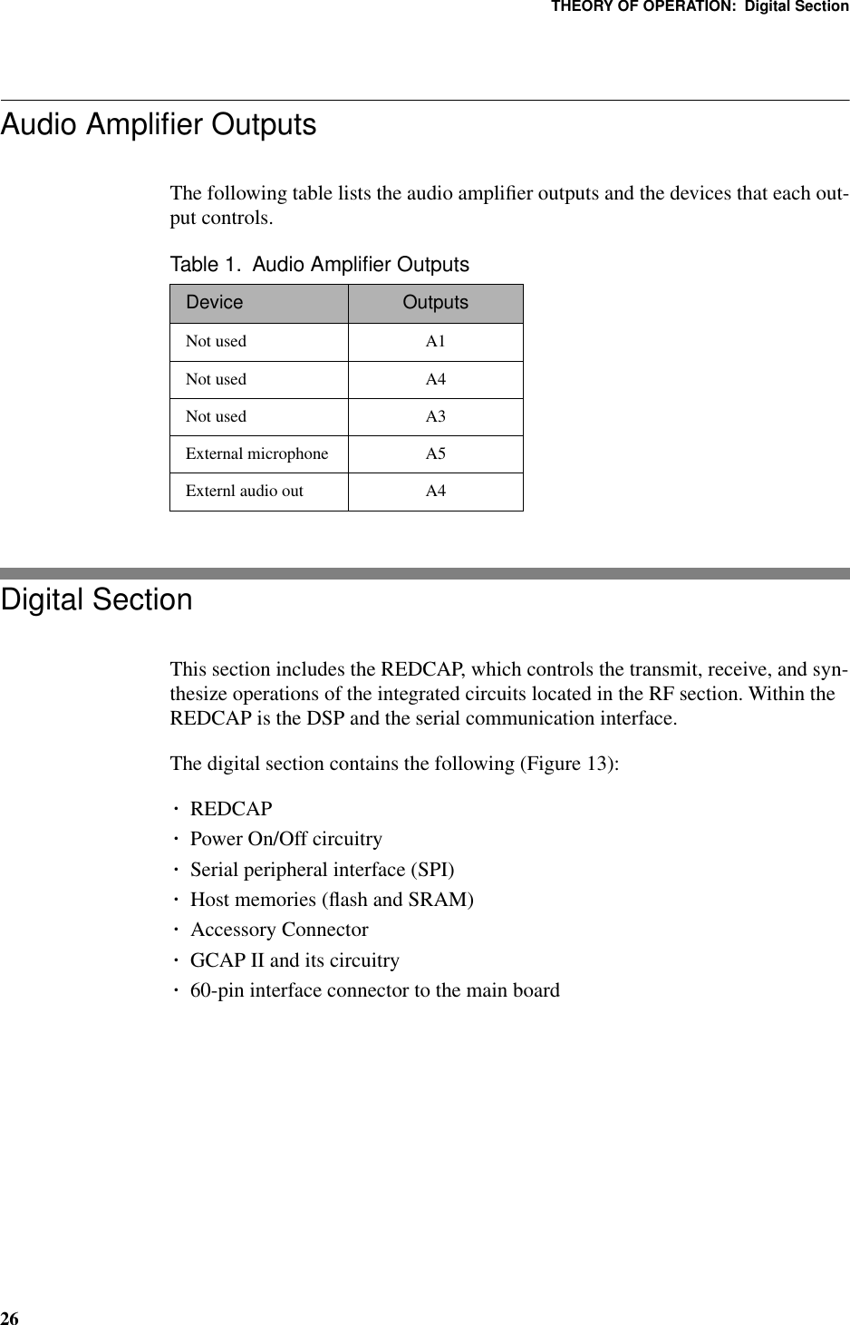
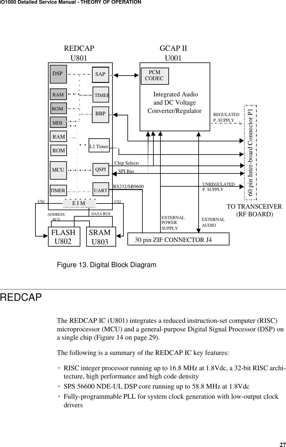
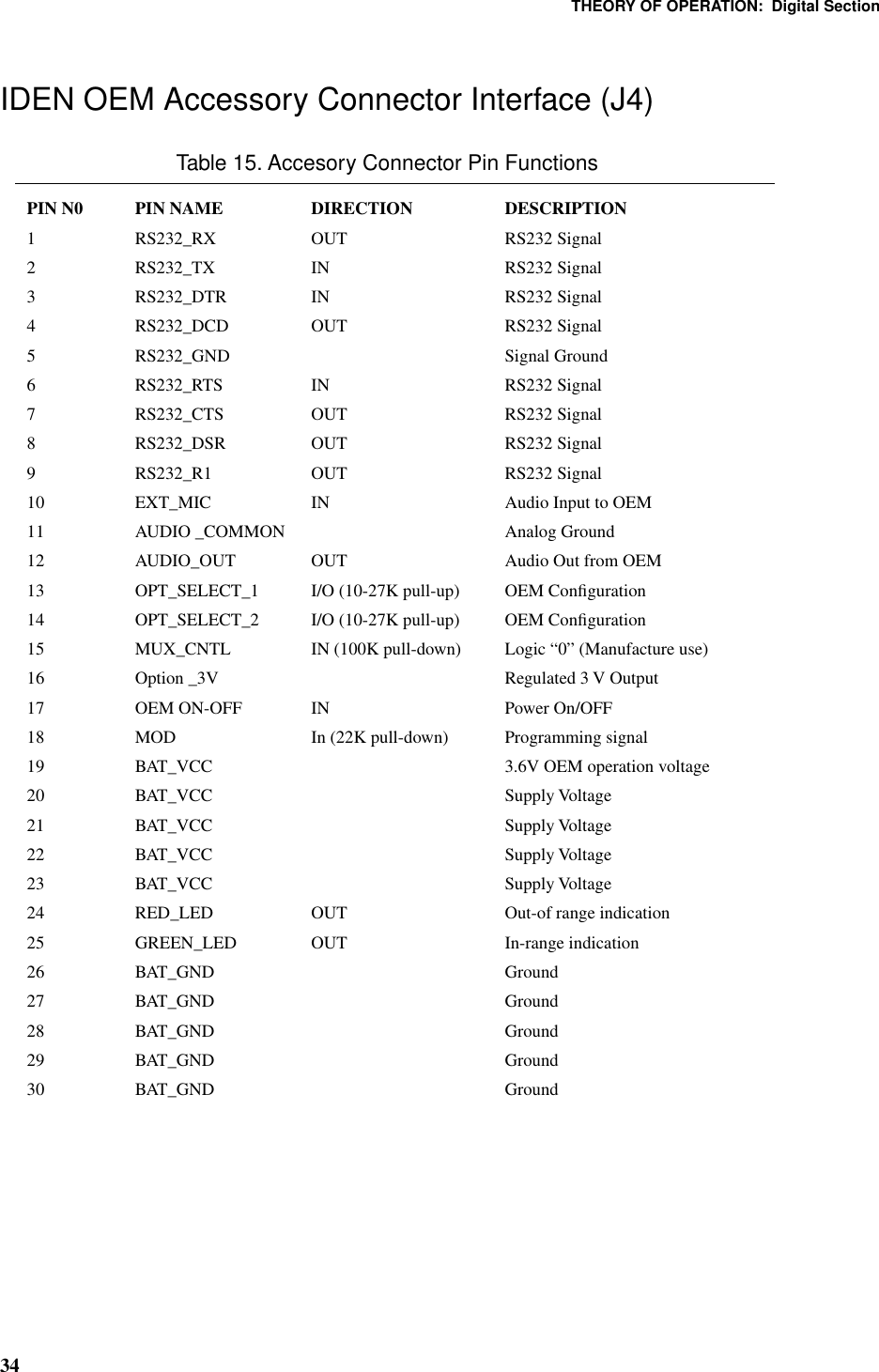
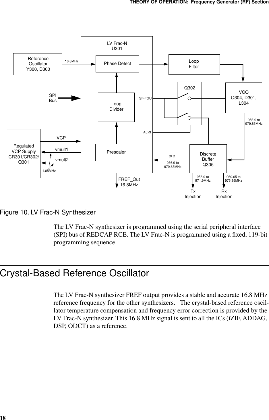
Exhibit 8 Technical Manual

 iO1000Wireless Modem Detailed Service Manual 7 OCT 1999¤       68P02953C80-O
 Manual Revisions Changes that occur after this manual is printed are described in the Field Manual Revisions (FMRs). The FMRs provide the most current instructions and component information. Copyright Information Motorola products described in this manual may include copyrighted Motorola computer programs stored in semiconductor memories or other media. Laws in the United States and other countries preserve for Motorola certain exclusive rights for copyrighted computer programs, including the exclusive right to copy or reproduce in any form the copyrighted computer program. Accordingly, any copyrighted Motorola computer programs contained in the Motorola products described in this manual may not be copyrighted or reproduced in any manner without the express written permission of Motorola. Further-more, the purchase of Motorola products shall not be deemed to grant either directly or by implication, estoppel, or otherwise, any license under the copyrights, patents, or patent applications of Motorola, except for the normal non-exclusive royalty-free license to use that arises by operation of law in the sale of the product. Trademarks The following is a registered trademark of Motorola, Inc.: ¥ iDEN® Reg. U.S. Pat. & Tm. Off.All other trademarks mentioned in this manual are trademarks of their respective companies. Patent Information This product is protected under one or more of the following patents:4817157, 4896361, 4857928, 5041793, 5060294, 5066923, 5134718, 5140156, 5239963, 5257411, 5287387, 5265219, 5289504, 5316168, 5317247, 5338396, 5389927, 5406588, 5424921, 5457376, 5460906, 5551063, 5557079, 5596487, 5615412, 5638403, 5559468, 5469465, 5170413, 5140615, 5519730, 5241544, 5584059, 5574992, 5396656, 5487091, 5533004, 5299199, 5343499, 5369501, 5509031, 5515379, 5528723, 5598417, 5066923, 5241650, 5278833, 5359696, 5548631, 5410632, 5440582, 5457735, 5457818, 5471670, 5477550, 5481537, 5566181, 5229767, 5208804, 5295140, 5381449, 5440590, 5467398, 5490230, 5620242, 5623523, 5655913© Copyright 1999, Motorola, Inc. All rights reserved.
 iii              For the Safe and Efficient Operation of Your Radio, Observe these Guidelines: Your radio contains a transmitter and a receiver. When it is  ON , it receives and transmits radio frequency (RF) energy. The radio operates in the frequency range of 806 MHz to 866 MHz and employs digital modulation techniques. This product is authorized under FCC Rule Part 47CFR 2. 1091 (b), which states that it should be used in such a way that a separation distance of at least 8 inches (20 cms) is normally maintained between the radio’s antenna and the body of the user or nearby persons. When you use your radio product, the system handling your call, controls the power level at which your radio product transmits. The output power level typically may vary over a range from 0.0024 watts to 0.7 watts. Exposure To Radio Frequency Energy Your Motorola Radio Product is designed to comply with the following national and international standards and guidelines regarding exposure of human beings to radio frequency electromagnetic energy:• United States Federal Communications Commission, Code of Federal Regulations; 47 CFR part 2 sub-part J• American National Standards Institute (ANSI) IEEE. C95. 1-1992• National Council on Radiation Protection and Measurements (NCRP). Report 86 • International Commission on Non-Ionizing Radiation Protection (ICNIRP) 1998• European Committee for Electrotechnical Standardization (CENELEC), ENV 50166-2, 1995 E• National Radiological Protection Board of the United Kingdom, GS 11, 1988• Verband Deutscher Elektrotechniker (VDE) DIN-0848• Department of Health and Welfare Canada. Safety Code 6 Antenna and Installation Considerations •    All equipment must be properly installed in accordance with Motorola installation instructions.•    To assure compliance with United States FCC regulations on RF exposure, the user of the equipment must position the antenna in such a way to maintain a separation of at least 8 inches (20 cms) between the antenna and the body of any user and nearby person.•    Ensure that the antenna is properly installed external to the vehicle and in accordance with the requirements of the antenna manufacturer/supplier.•    Use only the supplied or an approved antenna. Unauthorized antennas, modifications, or attachments could impair call quality, damage the modem, or result in violation of the ICNRP or the FCC. Interference to Medical and Personal Electronic Devices Most electronic equipment is shielded from RF energy. However, certain equipment may not be shielded against RF signals from your radio radio product. Pacemakers Do not operate the radio when any person is within 6 inches (0.15 meters) of the antenna. That person may be using a pacemaker, a hearing aid or other personal electronic device which may not be adequately shielded. Hearing Aids Some radio products may interfere with some hearing aids. In the event of such interference, you may want to consult your hearing aid manufacturer to discuss alternatives. Other Medical Devices If you use any other personal medical device, consult the manufacturer of your device to determine if it is adequately shielded from external RF energy. Your physician may be able to assist you in obtaining this information. SAFETY AND GENERAL INFORMATION IMPORTANT INFORMATION ON SAFE AND EFFICIENTOPERATION. READ THIS INFORMATION BEFORE USING YOURINTEGRATED MULTI-SERVICE RADIO PRODUCT.
 iv RF energy may affect improperly installed or inadequately shielded electronic operating and entertainment systems in motor vehicles. Check with the manufacturer or representative to determine if these systems are adequately shielded from external RF energy. Also check with the manufacturer of any equipment that has been added to the vehicle. SAFETY AND GENERAL USE WHILE DRIVING Check the laws and regulations on the use of radio products in the area where you drive. Always obey them.When using the radio product while driving, please:• Give full attention to driving and to the road• Pull off the road and park before using the product if driving conditions so require.                                              POTENTIALLY EXPLOSIVE ATMOSPHERES Turn off your radio product when you are in any area with a potentially explosive atmosphere, unless it is a radio product type especially qualified for use in such areas (for example, Factory Mutual Approved). Sparks in a potentially explosive atmosphere can cause an explosion or fire resulting in bodily injury, or even death. Note: The areas with potentially explosive atmospheres referred to above include fueling areas such as: below decks on boats; fuel or chemical transfer or storage facilities; areas where the air contains chemicals or particles such as grain, dust or metal powders; and any other area where you would normally be advised to turn off your vehicle engine. Areas with potentially explosive atmospheres are often, but not always posted. Do not transport or store flammable gas, liquid, or explosives in the compartment of your vehicle which contains your radio or accessories.In the United States, Vehicles powered by liquefied petroleum gas (such as propane or butane) must comply with the National Fire Protection Standard (NFPA-58). For a copy of this standard, contact the National Fire Protection Association. One Batterymarch Park, Quincy, MA 02269, Attn: Publications Sales Division.!W A R N I N G!     !W A R N I N G!OPERATIONALWARNINGS    INTERFERENCE TO OTHERELECTRONIC DEVICES
 v  BLASTING CAPS AND AREAS To avoid possible interference with blasting operations, turn off your radio product when you are near electrical blasting caps, in a blasting area, or in areas posted: "Turn off two-way radio". Obey all signs and instructions. FOR VEHICLES EQUIPPED WITH AN AIR BAG An air bag inflates with great force. DO NOT place objects, including communication equipment, in the area over the air bag or in the air bag deployment area. If the communication equipment is improperly installed and the air bag inflates, this could cause serious injury.Installation of vehicle communication equipment should be performed by a professional installer/technician qualified in the requirements for such installations. An air bag’s size, shape,and deployment area can vary by vehicle make, model, and front compartment configuration (for example, bench seat vs. bucket seats).Contact the vehicle manufacturer’s corporate headquarters, if necessary, for specific air bag information for the vehicle make, model, and front compartment configuration involved in your communication equipment installation.                                           DAMAGED ANTENNAS Do not use any radio product with a damaged antenna. If a damaged antenna comes into contact with your skin, a minor burn can result. CLEANING INSTRUCTIONS Clean the external surfaces of the radio product with a damp cloth, using a mild solution of dishwashing detergent and water. Some household cleaners may contain chemicals that could seriously damage the radio product. Avoid the use of any petroleum-based solvent cleaners. Also, avoid applying liquids directly on the radio product.!W A R N I N G!!C a u t i o n OPERATIONAL   WARNINGS    OPERATIONALCAUTION
 vi IMPORTANT INFORMATION   FOR EVERY MANUFACTURER TO WHOM THESE PRODUCTS ARE RESOLD iO1000 modems that we are supplying  to you for incorporation into the final product are components that when connected to the power supply can receive and transmit radio signals. In the United States, the Federal Communications Commission requires that many radio transmitting devices must obtain approval before being offered on the market, unless the device is exempt   While the iO1000 modem has been designed to meet applicable FCC requirements, provided in the code of Federal Regulation 47CER part II subpart J and 47CER part S, the Final Product’s compliance with the FCC’s requirements, including RF energy expo-sure requirements, must reflect product usage, posi-tioning of the iO1000 within the product, the type of antenna used, the,location of the antenna, and other factors that may vary with the design and nature of the Final Product. Therefore, compliance with such FCC requirements can only be determined by an assess-ment of the Final Product.It is important that any manufacturer to whom the   iO1000 modem is resold for use in the Final Product also recognize that he/she will have the responsibility for taking all necessary steps to ensure that the Final Product meets any applicable FCC requirements and for obtaining any necessary approval from the FCC for sale and operation of the Final Product. To the extent that this may require development of user information or guidance to be provided to each pur-chaser of the Final Product, this will also be the responsibility of the manufacturer.
 vii iO1000 Detailed Service Manual - MODEL SPECIFICATIONS FOR F2581A MODEL SPECIFICATIONS FOR F2581A Specifications subject to change without notice. GENERAL RECEIVER TRANSMITTER FCC Designation: Receiver Type: RF Pulse Avg. Power: 0.6 W Temperature Range: Frequency Range: 851-866 MHz Frequency Range:Operating: –25°C to +60°C Bandwidth: 15 MHz 806-821 MHz Storage (w/o battery): –40°C to +85°C Channel Spacing: 25 kHz Frequency Stability:Supply Voltage: Frequency Stability: Locked to base: 0.2 ppm Nominal: 3.6 Vdc Locked to base: 0.2 ppm Not locked to base: 5 ppm Range: 3.4 to 3.8 Vdc Not locked to base: 5 ppm Sensitivity (10%) BER: Spurious Emissions:Dimensions (H x W x D)               111.5 x 56.5 x 27.5 mm 851-866 MHz: – 111 dBm Conducted: – 43 dBW    Weight (with lithium battery): 126 g Selectivity:25 kHz Adjacent Channel: 60 dB Radiated: – 43 dBW     Modulation Type Quad 4/16/64QAM Image (typical): 55 dB Emissions Designator: 20K0D7W Adjacent Channel . Power  at +/- 25kHz           -60dB
 MODEL SPECIFICATIONS FOR F2581A viii
 1 iO1000 Detailed Service Manual - OVERVIEW CHAPTER 1 OVERVIEW INTRODUCTION The iO1000  Detailed Service Manual  contains the information necessary to iden-tify and fix problems in the iO1000 OEM Module. This unit is based on digital technology and is designed to operate on integrated Digital-Enhanced Network (iDEN) systems.Service for the iO1000 unit is based on the substitution method: a faulty part is replaced by a working one, providing quick service to the customer. For example, if the battery is faulty, it is replaced. If the unit requires more complete testing or service than is available at the basic level, it is sent to the field-level service facil-ity, serviced, and returned to the iDEN Customer Care Center (ICC). Note: Before operating or testing this unit, please read the  Safety and General Information  section in the front of this manual. Digital Modulation Technology The iO1000 is an 806-866 MHz unit that can operate in three modes:  dispatch ,  interconnect , and  multi-service . It uses two digital technologies: Quad 16QAM and Time Division Multiple Access (TDMA). Quadrature Amplitude Modulation (QAM)  is a modulation technique that trans-mits information by altering the amplitude and phase of the radio frequency (RF) signal. Data is converted into complex symbols, which alter the RF signal and transmit the information. When the signal is received, the amplitude and phase are converted back into symbols and then into the original data.In 16QAM, each of the 16 possible combinations of four bits is converted into a unique amplitude and phase. The traditional 25 kHz channel used for two-way radios is split into four 16QAM signals (subcarriers) that are transmitted simulta-neously. This technique can transmit 64 kbps in a single 25 kHz channel.The signal spectrum of the Quad 16QAM is shown in Figure 1 on page 2.
 OVERVIEW:  Digital Modulation Technology 2 Figure 1. Spectrum of IDEN Quad 16QAM Time Division Multiple Access (TDMA)  is used to allocate portions of the RF sig-nal by dividing time into six slots, one for each unit. Time allocation enables each unit to transmit its voice information without interference from another unit’s transmission.Transmission from a unit or base station is accommodated in time-slot lengths of 15 milliseconds and frame lengths of 90 milliseconds (see Figure 2 on page 3).0-10-20 10 20Frequency from Desired Channel Center(kHz)RL  0dBm                   10 dB/Power(dB)-10-20-30-40-50-60-70
 3 iO1000 Detailed Service Manual - OVERVIEW Figure 2. iDEN TDM Format Note that  Rx  (outbound) indicates base-to subscriber transmissions;  Tx  (inbound) indicates subscriber-to-base transmissions. The slots are paired and have a fixed offset of 19 milliseconds; their timings are synchronized by the iDEN system. The TDMA technique requires sophisticated algorithms and one digital-signal proces-sor (DSP) to perform voice compression/decompression and RF modulation/demodulation. Voice Compression Technology Voice is converted into a digital bit stream by sampling the voice signal at a high rate and converting the samples into numbers, which are represented by bits. A sample consists of eight bits. Approximately 8,000 samples per second (64 kbps) are required to maintain a reasonable quality. Voice compression  reduces the number of bits per second while maintaining the voice at an acceptable quality level. The iDEN system uses a coding technique called  Vector Sum Excited Linear Prediction (VSELP)  to compress voice to 4.2 or 8.0 kbps. The compressed voice-data bits modulate the RF signal. The compres-sion rate is based on the type of call (dispatch or interconnect) and the network configuration established by the local service provider.15ms15ms 15ms15ms 15ms 15ms 15ms 15ms 15ms 15ms 15ms 15ms 15ms15ms90ms 90ms15ms15ms 15ms 15ms 15ms 15ms 15ms 15ms 15ms 15ms 15ms 15ms15ms90ms  90msTxRxReceiver 4ms delayedTransmitting 6 of 6 slots continually.15ms15ms 15ms15ms 15ms 15ms 15ms 15ms 15ms 15ms 15ms 15ms 15ms15ms90ms 90ms15ms15ms 15ms 15ms 15ms 15ms 15ms 15ms 15ms 15ms 15ms 15ms15ms90ms  90msRxTxTransmitter 4ms delayedWhen turned on, scans for control station, then transmits one slot every six slots.Base Station Control ChannelPortable Unit
 OVERVIEW:  Voice Compression Technology 4 Adding error-correction bits to the coded-voice bits increases the required RF-transmission bit rate to approximately 7.4 kbps for the 4.2 kbps voice coder and 14.8 kbps for the 8.0 kbps voice coder. RF Transmission Bursts All RF transmissions within an iDEN system occur in 15-millisecond blocks called  bursts . An iDEN base station transmits bursts continuously on each RF fre-quency it uses. Transmission bursts from the stations are synchronized in time by signals received from the global positioning satellite (GPS) system. Each burst is numbered; the number is referred to as the  slot  number. All bursts occurring at a given time carry the same slot number.Inbound transmission bursts (sent from the unit) are offset 19 milliseconds from the outbound burst; the inbound burst begins 4 milliseconds after the end of the outbound burst (see Figure 2 on page 3). This offset in time allows the unit to appear capable of transmitting and receiving at the same time (it actually is switching rapidly back and forth between receiving and transmitting).In current iDEN systems, outbound transmissions range from 851-866 MHz; inbound transmissions are 45 MHz lower in frequency.An iDEN channel is created by grouping bursts so that their slot numbers differ by a number referred to as the repetition rate. The portable uses two repetition rates for interconnect voice calls: 6:1 and 3:1. A single frequency can handle six calls using a 6:1 repetition rate with the 4.2 kbps coder. Dispatch calls always use this rate. However, the audio quality of the 3:1 repetition rate with the 8.0 kbps coder is superior to the 6:1 rate with the 4.2 kbps coder. Most service providers config-ure the system and unit to allow only the 3:1 rate for interconnect calls.Calls are setup on a primary control channel (PCCH) in response to a request from a unit or a regular telephone connected to the Public Switch Telephone Network (PSTN). The PCCH is established by the base station equipment; typically, it is a 6:1 channel.The outbound PCCH carries system information and “pages” to specific sub-scriber units and asks them to respond if they are available for a call. Inbound PCCH transmissions carry responses to the “pages” and requests by subscriber units to set up calls. Inbound transmissions on the primary control channel only take 7.5 milliseconds and may be timed to occur in either half of a 15-millisecond burst. Using the above techniques, the iDEN system can operate six voice channels simultaneously in dispatch mode or three voice channels simultaneously in inter-connect mode on a single RF carrier at 25 kHz bandwidth.
 5 iO1000 Detailed Service Manual - CHAPTER 2 CHAPTER 2THEORY  OF OPERATION This section provides a detailed theory of operation for the iO1000 OEM module and its components: the receiver, transmitter, frequency generation unit, logic unit, and the audio and data circuits. Block Diagram Description The below figure shows the hardware block diagram of the iO1000 OEM Module. This  module includes two boards:RF and Logic. Figure 3. RF and Logic Connection Diagram RF Board The RF board is an 800 MHz RF transceiver. It includes frequency synthesizers, the transmitter circuitry, 0.6 Watt transmit power circuitry, receiver circuitry, and electronic T/R switch.LOGICBOARD RFBOARDRS-232/SB9600/JTAGOpt_SelDC PowerAudioOn/Off ControlDCSPISSI.MiscAntenna Connector
 THEORY OF OPERATION:  Block Diagram Description 6 The RF board is connected to the Logic Board through a 60-pin connector. Fol-lowing are functions of the RF Board: 1. Transmit (0.6 watt) - iDEN modulation of the RF carrier with baseband data signal. 2. Receive - Demodulation of received RF signal to generate baseband signal 3. Frequency Synthesizer Channels (806-825 MHz TX) and (851-870 MHz RX). Logic Board The Logic Board includes  a red cap that controls the transmit ter, receiver, and synthesizer operations of the integrated circuits located on the RF board. The red cap houses the DSP and the serial communication interface
 7 iO1000 Detailed Service Manual - THEORY OF OPERATION Transmitter Path Section This section includes a quasi-linear class AB power amplifier (PA) for linear mod-ulation of the iDEN portables. When the unit is transmitting data, the digital data is sent to the DSP.  When an audio is used, microphone audio is routed to the CODEC, where it is amplified and digitized by the A/D converter in the CODEC. 13-bit data is then sent from the CODEC to the DSP for processing.Figure 4 illustrates the transceiver circuitry path. Figure 4. Transceiver Circuitry Path The DSP performs VSELP data compression and generates digital I & Q words to be transmitted to the ADDAG. The signal then is sent to ADDAG at a rate of 48 K samples per second. The ADDAG provides the serial clock to the DSP and a frame sync pulse to tell the DSP to send a sample. Each sample is sent as a 16-bit I word followed by a 16-bit Q word and then some meaningless fill bits.The I word and the Q word are then converted to an analog differential pair by the ADDAG and amplified. The ADDAG also sends a 2.4MHz reference clock signal to the ODCT, together with a differential TSLOT pair that toggle whenever a TXE signal is received from the DSP. Once the TSLOT toggles, data is sent from the DSP ADDAG ODCT PAISOLATORMAIN VCOOFFSET VCOREF. OSC.A/SANTENNAIMAGEFILTERHOSTREDCAPControlCircuitryMUXDIGITALDATAU001 (GCAP)MICROPHONETXESERIALDATATSLOTfo  +150.9MHz301.8MHzTCLKDATAASWVBLINVNCTODSP CLKSERIAL CLKA/D CONV.DIGITIZEDVOICESPI CLKVCONTROLVDPSP I/O16.8MHzLevelShifter
 THEORY OF OPERATION:  Transmitter Path Section 8ADDAG to the ODCT. After receiving the data, the ODCT toggles the ASW line, which signals the ADDAG to turn on the PA and the antenna switch to start trans-mitting.ADDAGThe ADDAG (Analog-to-Digital/Digital-to-Analog Glue logic) converts the serial I & Q words to parallel I & Q words, truncates them to 8 bits and sends them to dual 8-bit D/A converters. The D/A converters take the digital I & Q words and convert them into analog signals, which then are filtered and amplified. The base-band filters have a 10 kHz pass band. The output is comprised of two separate low-level differential signals, I & Q. A differential output is used to minimize noise pickup, due to its inherent common mode rejection. The output signals are routed to the ODCT IC where the transmitter now becomes a closed loop.ODCTThe ODCT (Offset Direct Conversion Transmitter) is the heart of the transmitter; it incorporates an offset synthesizer and all of the circuitry necessary to implement a cartesian feedback closed-loop system. The iZIF offset synthesizer phase locks an external VCO at 301.8 MHz. This is divided down in the ODCT to 150.9 MHz in the quadrature generator of the internal image reject mixer. The divided down offset LO is then mixed with the main LO in the image reject mixer. The output of the mixer is the carrier frequency.The differential baseband signals from the ADDAG are input into the ODCT on pins 57-60. They go through a variable attenuator and are then summed with the down converted I & Q feedback. The baseband signal is then amplified and sent to the upmixers.The upmixers consist of two mixers, one for the I channel and one for the Q chan-nel. The output of the image reject mixer is split into quadrature (90 degrees phase difference) and is mixed with the baseband I & Q signals to produce an I and a Q signal at RF frequency. The two RF signals are then summed, producing a com-plex modulated RF signal (QAM). The signal is then output, differentially on pins 51 and 52.
9iO1000 Detailed Service Manual - THEORY OF OPERATIONBALUNThe differential RF signal is converted to a traditional single-ended (unbalanced) signal through the balun (balanced/unbalanced) circuitry. The balun is imple-mented using multilayer ceramic technology.SAW FilterThe signal is then routed to the SAW filter. The SAW filter further attenuates the residual image frequency and any out-of-band noise that may be present.RF Power AmplifierThe signal is then routed to the RF PA. The RF PA has an adjustable gain that can be varied from 30 dB to 36 dB. The gain is adjusted by varying the control voltage on pin 1 of the PA. The control voltage is supplied by a D/A converter in the ADDAG. The gain is tuned at the factory and should not require any adjustment; any change in the loop gain can result in the transmitter splattering into the adja-cent channel. The PA is turned on by supplying the battery voltage to pins 3, 5, and 7 of the PA through Q501. This is done only after the PA negative bias volt-ages have been applied to pins 1 and 4.CouplerAt the output of the PA is a high value inductor that is used to sample the signal and provide the necessary feedback for the linearization. A directional coupler is not needed because the isolator that follows provides the directivity. The sampled signal passes through an attenuator and is input to the ODCT at pin 37. The sam-pled signal is then mixed down to baseband in the downmixer, a quadrature mixer, and the resulting output is an I and a Q signal which is then summed with the input. This completes the closed loop.
THEORY OF OPERATION:  Transmitter Path Section10IsolatorThe isolator protects the PA from any impedance changes that may occur at the antenna. The isolator provides a constant impedance to the PA so that its gain does not vary depending on load, which could result in splatter. The isolator is a circu-lator with the third port internally terminated to absorb any reflected power from port 2.Antenna SwitchThe antenna switch consists of two PIN diodes, one series and one shunt. The diodes are biased On in transmit mode and Off in receive mode. The bias voltage is VDP (3.6Vdc pulsed). The DC return is through the isolator, since it is a DC short.Cartesian FeedbackiDEN transmitters use MQAM modulation, which requires a highly linear PA with wide dynamic range. Linear PAs are highly inefficient so a class AB PA is used for better efficiency and longer battery life. The class AB PA is fairly linear, but not totally; and this causes splatter in the RF spectrum around the transmitted frequency band. To reduce splattering into the adjacent channels and to meet sys-tem specifications, the transmitter uses cartesian feedback to linearize the PA and reduce splatter. Negative feedback is a commonly used method to linearize cir-cuits.Cartesian feedback is the process of down converting the feedback signal to base-band and summing it with the input signal in the I & Q paths separately. One can control the 180o phase shift at baseband more precisely than at RF frequencies. The ODCT is the heart of the cartesian feedback system, and as such, is the heart of the transmitter. There is a forward path and a feedback path in the transmitter. This a closed loop system and the loop cannot be opened without drastic conse-quences. See Figure 5 on page 11.The forward path includes the following:¥ODCT ASIC¥Balun¥Image filter
11iO1000 Detailed Service Manual - THEORY OF OPERATION¥Power amplifier¥Isolator¥Antenna switchThe feedback path includes the following:¥Feedback inductor¥Attenuator¥ODCT ASICFigure 5. Cartesian LoopAmplitudeAdjustIQLODOWNMIXER0° & 90°PhaseAdjust0° & 90°RF INUPMIXERRF OUTTransmitterOutput ∑∑∑
THEORY OF OPERATION:  Transmitter Path Section12Level Set and Phase TrainingLevel set training is performed to ensure that the RF PA is not driven into clip, which would result in excess splatter and out-of-band spurious emissions. During training, the DSP signal is disconnected from the forward path and an internal analog ramp generator is connected. The feedback is monitored and compared to the analog ramp. As the ramp amplitude increases and the RF PA begins to clip, the error voltage increases. See Figure 6 on page 12.When the error signal exceeds a pre-determined threshold, the ramp level is held and step attenuators are set to prevent the maximum-input signal level from exceeding the ramp level, which caused the clip. The ramp is allowed to decay to zero.Figure 6. Level Set TrainingNegative feedback is required to maintain system stability. Phase training is done to ensure that the feedback is negative (180o). The phase shift of the loop consists of the sum of the delays of several modules and components, such as SAW filters and amplifiers.The Q channel is set to zero and a positive signal is sent to the I channel. If there is negative feedback, the I feedback channel is negative and no signal should be present in the Q channel. The phase of the LO down mixer is adjusted to maxi-mum negative feedback. The phase-training algorithm is iterative. The I signal •ErrorVoltagePredeterminedThresholdVoltageComparatorTriggerSampleand HoldInOut++--+--SoftwareControlledSwitchRampGeneratorAttenuatorFromADDAG
13iO1000 Detailed Service Manual - THEORY OF OPERATIONbecomes negative and the LO phase is adjusted. This phase adjustment is per-formed twice on the I channel with positive and negative values. See Figure 7 on page 13.Figure 7. Phase TrainingReceiver Path SectionThe iO1000 receiver is a double-conversion, superheterodyne receiver (see Figure 8 on page 14). It operates in the commercial portion of the land-mobile receiver band (851-866 MHz). The receiver takes an incoming RF signal, down-converts it to a filtered109.65 MHz frequency (IF stage), and converts it to base band. The signal is then digitized.The receiver has automatic gain control (AGC) to maintain good linearity over a wide range of incoming signals. The AGC circuitry also prevents clipping of high-level signals.ILODOWNMIXER0° and 90°PhaseAdjust0° and 90°RF INUPMIXERSwitchComparatorRF OUTTransmitterOutput ∑∑+-
THEORY OF OPERATION:  Receiver Path Section14Figure 8. Receiver Path DiagramThe receiver path includes the following components:Antenna SwitchThe antenna switch routes the received signal from the antenna to the receiver front-end. During transmit mode, this switch disconnects the receiver path and connects the antenna to the transmit path. This switch is optimized to have a very low loss.Preselector SAW FilterThe preselector SAW filter protects the RF amplifier from strong, out-of band sig-nals. It has a pass band from 851 MHz to 866 MHz.Down MixerThe down mixer is an active mixer. It converts RF input to IF output. The mixer LO drive is provided from the VCO buffer in the frequency-generation portion of the unit. The LO drive is provided to the mixer through a saw filter.3-Pole Crystal FilterThe 3-pole crystal filter provides narrow bandpass selectivity centered at the IF frequency (109.65 MHz). The crystal-filter bandwidth allows a single 21 kHz channel to pass through with little attenuation. The filter provides rejection to adjacent channels.RF InputAttenuator ON/OFFControl from iZIF From VCO Buffer Amp1st LO Injection960.65-975.65MHz16.8MHz REF fromFran-N SynthesizerSAWFilterDown Mixer(Active)1st IF Filter109.65MHzCrystalIFLORFiZIF and PeripheriesData Out toADDAG and DSP219.3MHz VCO2nd LO InjectionControl VAntennaSwitch0 or 10dBAttenuatorSAWFilter851-866MHziZIF
15iO1000 Detailed Service Manual - THEORY OF OPERATIONiZIF ICThe iZIF IC performs the following functions:¥Implements AGC¥Down converts IF into baseband I and Q¥Synthesizes the second VCO frequency and TX offset oscillator¥Sends received data to the DSP through the ADDAGThe iZIF takes the IF signal as its input, and outputs differential I and Q baseband signals as well as differential RSSI information. The signal path inside this IC can be divided into three stages: IF pre-amp, down conversion mixer, and baseband filters.The first part of the IF pre-amp stage is a 20 dB step attenuator that is controlled by the iZIF AGC circuitry. This step attenuator is used to protect the IC from over-load during strong signal conditions. The next part of this stage is the pre-amp. This is an amplifier that has been optimized for noise figure and gain. The last part of the IF pre-amp stage is the variable attenuator, which has been optimized to maintain a constant third-order intercept point.The next stage in the iZIF lineup is the down conversion mixer. This is a quadra-ture type of mixer. Its inputs are the IF and second LO signals (see “Second Local Oscillator (LO)” on page 19), and its outputs are baseband I and Q signals. The last stage in the iZIF is the baseband filters. These are lowpass filters that pro-vide the IF selectivity for the iZIF. Baseband I and Q signals go through these fil-ters.Receiver Signal FlowThe receiver can be divided into two parts. The first part is the front-end, which consists of the antenna switch, preselector SAW filter, and the down mixer. The second part is the back-end which consists of the 3-pole crystal filter, and the iZIF IC.The received signal goes through the front end the following way. During receive mode, the antenna switch connects the antenna to the receiver path. The received signal (RF) goes through the preselector SAW filter which only lets through the desired frequency band (851-866 MHz) and attenuates out-of-band signals and the image frequency. In the next stage, the down mixer, the signal is down converted from the RF frequency to a lower one called the intermediate frequency (IF).
THEORY OF OPERATION:  Frequency Generator (RF) Section16The mixer has two inputs (RF and first LO) and one output (IF). The first LO sig-nal is generated at a frequency of 109.65 MHz above the received frequency. For example, if the RX is 851 MHz, the first LO frequency will be 960.65 MHz. The first LO signal is supplied by the main VCO (see “Main VCO Synthesizer” on page 19).In the back-end of the receiver, the signal goes through the 3-pole crystal filter. This filter provides a narrow bandpass selectivity (21 kHz) for a 25kHz channel centered at 109.65 MHz, providing rejection to adjacent channels. The signal is then fed into the iZIF IC input (pin D1), which mixes it down to baseband I and Q. This information is sent to the ADDAG IC for digitizing prior to sending it to the DSP.Frequency Generator (RF) SectionThis section contains the following main components in the RF board:¥Low Voltage (3 Volt) Fractional-N (LV Frac-N) synthesizer¥Crystal-Based Reference Oscillator Circuit¥Discrete voltage controlled oscillator (VCO) circuit¥Second local oscillator (LO)¥DSP phase locked loop (PLL)¥Host system clock synthesizerAll frequencies in the iO1000 originate from the 16.8 MHz reference frequency provided by the Low Voltage Fractional-N synthesizer and the crystal-based refer-ence oscillator circuit. The UM5 crystal generates the 16.8 MHz signal, which is DC voltage-warped (or tuned) and temperature-compensated using the internalD/A converter in by the Low Voltage Fractional-N ASIC. See Figure 9 on page 17.
17iO1000 Detailed Service Manual - THEORY OF OPERATIONFigure 9. Frequency GeneratorLow Voltage Fractional-N (LV Frac-N) SynthesizerThis synthesizer provides the temperature compensation and frequency error cor-rection for the crystal-based reference oscillator, generates the control voltage for the main VCO, shuts off the buffer circuitry and main VCO in battery-save mode, and acts as a phase detector for the main VCO. The 16.8 MHz frequency is used as a reference for all frequencies generated in the portable.In the phase detector, the LV Frac-N synthesizer compares the divided 16.8 MHz reference to the divided-down LO. The output of the detector is the control volt-age for the main VCO. The feedback loop keeps the receive and transmitter fre-quencies locked and allows frequency transitions in a short period of time (lock time less than 3 milliseconds).The LV Frac-N controls the power to the main VCO and buffer circuitry in bat-tery-save mode. It switches the superfilter supply to the VCO and buffer on and off using a dual-transistor array, Q302 (see Figure 10 on page 18).Second VCO219.3MHzDSP58.3MHzSynthesizerU850Offset VCO301.8MHz16.8MHz16.8MHzPre-scaler Main VCO956.9-975.65MHz(Discrete)Q304LV Fractional - NSynthesizer(ASIC)U3012.1MHz:8ODCT(ASIC)U510150.9 x 2109.65 x 2DSP1.2MHzSerialPeripherialInterface(SPI) Clock16.8MHzCrystalRef Osc16.8MHzY300Buffer(Discrete)Q305ToTx and RxCircuitiZIFU601
THEORY OF OPERATION:  Frequency Generator (RF) Section18Figure 10. LV Frac-N SynthesizerThe LV Frac-N synthesizer is programmed using the serial peripheral interface (SPI) bus of REDCAP RCE. The LV Frac-N is programmed using a fixed, 119-bit programming sequence.Crystal-Based Reference OscillatorThe LV Frac-N synthesizer FREF output provides a stable and accurate 16.8 MHz reference frequency for the other synthesizers.   The crystal-based reference oscil-lator temperature compensation and frequency error correction is provided by the LV Frac-N synthesizer. This 16.8 MHz signal is sent to all the ICs (iZIF, ADDAG, DSP, ODCT) as a reference.16.8MHzReferenceOscillatorY300, D300SPIBusVCPvmult1vmult21.05MHzRegulatedVCP SupplyCR301/CR302/Q301LV Frac-NU301Phase DetectLoopDividerPrescalerFREF_Out16.8MHzSF-FGUAux3pre956.9 to979.65MHzTxInjectionLoopFilterQ302 VCOQ304, D301,L304956.9 to979.65MHz960.65 to975.65MHz956.9 to971.9MHzDiscreteBufferQ305RxInjection
19iO1000 Detailed Service Manual - THEORY OF OPERATIONMain VCO SynthesizerThis synthesizer consists of the crystal-based reference oscillator, Low Voltage Fractional ASIC, and main VCO circuit. It produces the RF signal to down-con-vert the received signal to the first IF frequency (109.65 MHz) and up-convert the transmitter IF frequency (150.9 MHz) to the transmit RF frequency.The main VCO receives its control voltage from the LV Frac-N to determine the oscillation frequency. It outputs its local oscillation frequency through a discrete buffer circuit that allows matching and gain. Part of this frequency is fed back to the pre-scalar input of the LV Frac-N to complete the loop.Second Local Oscillator (LO)This circuit supplies the LO signal to the quadrature down conversion mixer inside the iZIF in the receiver lineup (see “iZIF IC” on page 15).The second LO consists of a VCO, loop divider, phase detector, reference fre-quency, and loop filter. The loop divider and phase detector are internal to the iZIF.   The reference frequency is obtained by taking the 16.8 MHz crystal refer-ence signal into pin 21 of the iZIF and then dividing it down inside the IC to get 2.1 MHz. The loop filter and VCO circuits are external to the iZIF.   Although the IF frequency is 109.65 MHz, the VCO oscillates at 219.3 MHz. The VCO signal is divided by two inside the iZIF to get the desired 109.65 MHz.The VCO is run at twice the LO frequency to avoid the coupling of its signal into the iZIF preamp to eliminate the possibility that it will mix with itself at the down mixer.   The VCO resonator circuit consists of L607, C639, CR601, and C627. The loop filter determines how fast the second LO locks on frequency and how big the LO spurs are.   This circuit consists of R601, R602, C625, and C626.
THEORY OF OPERATION:  Frequency Generator (RF) Section20ADDAG ASICThe ADDAG is an acronym for A/D + D/A + Glue. The ADDAG IC is designed to be an interface between the system DSP, which is digital, and the custom transmit-ter and receiver ICs, which are primarily analog.A 16.8 MHz signal from pin 2 of Y300 Crystal sine_out is routed to pin K9 xtal input of the LV Frac-N synthesizer. The signal is buffered to produce a 16.8 MHz reference oscillator.; it goes out pin K6 of the LV Frac-N synthesizer and is routed to pin A5 of the ADDAG.The interface to the transmitter consists primarily of two 8-bit D/A converters with programmable sampling rates and filter bandwidths. The interface to the receiver consists primarily of a single, 10-bit A/D converter, which is multiplexed to convert I, Q, and RSSI signals captured from the output of the iZIF IC. The ADDAG IC includes a D/A converter for PA bias control. The voltage supply cir-cuit comes from VCC4 and VCC6.The inputs to the receiver path consist of three sample and hold circuits which are used to simultaneously sample the I, Q, and RSSI signals coming from the iZIF IC. To help maximize dynamic range and noise performance, these three input signals are fully differential, and therefore require a total of six pins on the ADDAG IC (pins INI, INIB, INQ, INQB, AGC, and AGCB). The sample and hold circuits are programmed for a 48ksps sampling rate.After sampling, the three input signals are multiplexed sequentially as differential signals to a single 10-bit A/D converter. The outputs of the A/D converter are cap-tured by a shift register, formatted, then sent out as a continuous serial data stream at the same rate as the internally generated serial clock signal. To make the output words DSP compatible, they are formatted as fractional, 2’s complement data words, with the MSB being left justified to turn the 10-bit words from the A/D converter into 16-bit output words. The serial output port is designed to produce a 48 kHz frame sync signal (pin SFS) at the start of each I word transmission. Immediately following the transmis-sion of the I word, the corresponding bits for the Q and AGC words are sent out in sequence over the serial port (pin SRD). This corresponds to having an SSI inter-face which uses a continuous clock in the network mode of operation. The output serial clock/data rate is 2.4 MHz (pin SCK).
21iO1000 Detailed Service Manual - THEORY OF OPERATIONODCT ASIC Offset VCOThe offset VCO is a discrete VCO that is controlled by the offset synthesizer in the iZIF. The frequency of the offset VCO is 301.8 MHz which is divided by two to 150.9 MHz in the ODCT and mixed with the main VCO to generate the transmit frequency.Transceiver CircuitryAll the transceiver circuitry is located on the main board. This board is divided into the following sections:¥Global Control Audio Power II (GCAP II) circuitry¥DC voltage distribution¥Audio circuitry¥Digital (REDCAP and associated circuitry)¥Transmitter path¥Receiver path¥Frequency generating (RF)The keypad contains the high-audio speaker, microphone, and keypad circuitry.Global Control Audio Power II (GCAP II) CircuitryThe GCAP II integrated circuit (IC) contains the following:¥Two BUCK/BOOST switching power supplies¥2.775Vdc/5.0Vdc regulator¥3.0Vdc/5.0Vdc regulator¥Linear 2.775Vdc to 3.6Vdc regulator in 8 steps ¥Linear 2.775Vdc to 1.8Vdc regulator in 8 steps¥2.775Vdc to 3.6Vdc low-current reference¥Analog/digital portions of a real-time clock (RTC)¥Charge pump output¥Power amplifier (PA) high-end regulator adjustable in 16 steps¥Battery charger
THEORY OF OPERATION:  Global Control Audio Power II (GCAP II) Circuitry22¥8-bit D/A converter¥10-channel, 8-bit A/D converter¥Square-wave output to generate negative supply voltages¥Control logic¥Audio CODEC with serial interface¥Earpiece amplifier¥Speaker amplifier¥Alert amplifier¥Two microphone amplifiers¥Auxiliary amplifier¥Sim card level shifters¥Serial peripheral interface (SPI)¥DSC-bus buffersThe GCAP II IC has the following specifications:¥Multiple lithium-ion cell input configuration¥Shutdown current: 10µA maximum¥Standby current mode: 400µA¥Internal PMOS pass devices¥Serial peripheral interface read/write interface¥Auxiliary battery switch control¥100-pin dual die QFP IC packageThe GCAP II IC is designed to support the needs of portable cellular telephone products. It provides the necessary control, audio, and regulator functions. The following functions are provided:¥Turn on control signals to properly activate the unit¥Turn off control signals to turn off the unit if an error is detected¥Audio amplification for the speaker¥Audio amplification for the alert¥Audio amplification for the external audio¥Audio amplification of the microphone¥13-bit linear audio CODEC¥Band-gap reference voltage¥Linear regulation of DC voltages¥Two BUCK/BOOST switching regulators¥Operational amplifiers for use in the battery charger¥Internal D/A conversion for the battery charger
23iO1000 Detailed Service Manual - THEORY OF OPERATION¥8-channel, 8-bit A/D conversion¥PA high-end regulation¥Real-time clock (RTC)DC Voltage DistributionThe iO1000 unit operates with a low-level supply voltage of 3.0Vdc, nominal-level voltage of 3.6Vdc, and high-level voltage of 4.2VdcThe DC voltage distribution of the iO1000 radio is supported by the GCAP II IC (Figure 11 on page 24). This IC supplies regulated power to the radio using its lin-ear requlators, V1, V2, and V3.A discrete regulator on the RF board supplies 2.775Vdc to both the receive and transmit circuitry, while V2 GCAP II linear regulator supplies 2.775Vdc to the clock buffers and low-voltage sense comparator. V1 GCAPII linear regulator sup-plies 2.775Vdc to the memories and V3 linear regulator supplies 1.875Vdc to the DSP and MCU cores. Additionally, an external 3.0Vdc linear regulator on the logic board supplies power to the accessories. Several sections of the radio are connected directly to the external power supply, which supplies Raw_B+ and Fused_B+.The external power supply is connected to the accessory connector J4 pins 19 through 23 (+) and 26 through 30 (-). These pins supply the Raw_B+ to the RF TX power amplifier. The Optional B+ output of the U005 regulator supplies 3.0V to the accessories through the accessory connector. Raw_B+ is routed through F001 (Fuse) becoming Fused_B+, which provides power to the GCAP II IC..The battery is connected to the J9003 pins 1 (+) and 2 (-). These pins supply the Raw_B+ to the RF TX power amplifier. The Optional B+ output of the U005 reg-ulator supplies the accessories through the bottom connector. Raw_B+ is routed through F001 (Fuse) becoming Fused_B+, which goes through the main FET and provides power to the GCAP II IC.
THEORY OF OPERATION:  Audio Circuitry24Figure 11. DC Power Distribution DiagramAudio CircuitryAudio circuitry consists primarily of the audio amplifiers and coder/decoder (CODEC) integrated in GCAP II IC. Its purpose is the future support of voice.RF PAFilterGCAP IILINEAR REG. V2;2.775V, 200mAGCAP IILINEAR REG. V1;2.775V, 60mAGCAP IILINEAR REG. V3;1.875V, 120mAGCAP II Vref;(tracks V2)2.775V, 5mAFuseLM2981;3.0V, 100mARAW_B+Raw_B+LM2664;2.775V InverterODCTSuper Filter;2.775V, 30mADrain SwitchODCT Up-mixeriZIF, LVFrac-N, Mixer, VCO, ADDAGFLASH, SRAMRedcap QVccH,Accessory VddExt. Memory Bus, SPI and ESSI PortsREDCAP DSP & MCU COREFilt_B+Fused_B+Filt_B+Fused_B+Vcc2Vcc2Vcc6Vcc2Vcc4Vcc3Clock Buffers, Low Volt. ComparatorVcc5Vcc1Opt_B+ (to Accessory Connector)VREFRF PA BIASNeg_supLOGIC BOARDRF BOARDRaw_B+
25iO1000 Detailed Service Manual - THEORY OF OPERATIONThe GCAP II consists of active RC filters, digital filters, variable attenuators, an analog-to-digital converter (ADC), a digital-to-analog converter (DAC), and a microphone amplifier.The average voice signal has a frequency band of approximately 300-3400 Hz. Low-pass filters are set up to provide the optimum response to the signal while fil-tering out high-level frequencies. Input signals from the microphone are amplified by the GCAP II internal op-amp and this amplified signal is converted from ana-log to digital in the ADC. These signals are then digitally filtered and transferred to the DSP core for further processing.Received analog signals are converted to digital signals by the ADDAG, then sent to the DSP for processing. The DSP then sends the processed signals to the CODEC, where they are converted from digital to an analog audio signal in the DAC. The DAC output is low-pass filtered to attenuate any out-of-band noise.From this point, the audio signal is sent to the GCAP II output ampli-fier A4 - the external audio output. Figure 4 indicates the circuitry path of the audio components.The iO1000 accepts audio input from the external microphone and sends the received audio to the external audio output. Figure 12. iDEN Audio Circuitry PathMCORE DSPMDIESSI1QSPI BusInbound AudioInt.MicExt.AudioOutExt.AudioInAUXMICMICINGCAP-IIReg 00Reg 06CODECA/DCODECD/ACDC_ENAUDOGAUDIGAUDOSAUDISEXTOUTA1A4A3A5PGAPGA
THEORY OF OPERATION:  Digital Section26Audio Amplifier OutputsThe following table lists the audio amplifier outputs and the devices that each out-put controls.Digital SectionThis section includes the REDCAP, which controls the transmit, receive, and syn-thesize operations of the integrated circuits located in the RF section. Within the REDCAP is the DSP and the serial communication interface.The digital section contains the following (Figure 13):¥REDCAP¥Power On/Off circuitry¥Serial peripheral interface (SPI)¥Host memories (flash and SRAM)¥Accessory Connector¥GCAP II and its circuitry¥60-pin interface connector to the main boardTable 1.  Audio Amplifier OutputsDevice OutputsNot used A1Not used A4  Not used A3External microphone A5Externl audio out A4
27iO1000 Detailed Service Manual - THEORY OF OPERATIONFigure 13. Digital Block DiagramREDCAPThe REDCAP IC (U801) integrates a reduced instruction-set computer (RISC) microprocessor (MCU) and a general-purpose Digital Signal Processor (DSP) on a single chip (Figure 14 on page 29).The following is a summary of the REDCAP IC key features:¥RISC integer processor running up to 16.8 MHz at 1.8Vdc, a 32-bit RISC archi-tecture, high performance and high code density¥SPS 56600 NDE-UL DSP core running up to 58.8 MHz at 1.8Vdc¥Fully-programmable PLL for system clock generation with low-output clock driversFLASHU802 SRAMU803GCAP IIU001Integrated Audioand DC Voltage Converter/Regulator 30 pin ZIF CONNECTOR J4TO TRANSCEIVER(RF BOARD)REDCAPU801DSPRAMROMMDIRAMROMMCUSAPTIMERBBPL1 TimerTIMER UARTE I MRS232/SB960060 pin Inter-board Connector P1EXTERNALPOWERSUPPLYEXTERNALAUDIOPCMCODECREGULATEDP. SUPPLYUNREGULATEDP. SUPPLYSPI BusChip SelectsDATA BUSADDRESSBUSCS0 CS2QSPI
THEORY OF OPERATION:  Digital Section28¥512 KB x 32 on-chip MCU RAM¥512 KB x 24 DSP program RAM¥Queued serial peripheral interface to communicate with external peripherals¥Serial communications interface with baud-rate generator up to 525 kbps¥On-chip Emulator (OnCE) integrated with JTAG port compliance¥Interrupt, general-purpose I/O, and keypad interface pins¥Very-low power CMOS design¥Wait, stop, and doze low-power standby modes
29iO1000 Detailed Service Manual - THEORY OF OPERATIONFigure 14. REDCAP DiagramSIM(5)STDBSRDBSFSB(2)SCKB(2)STDASRDASFSA(2)SCKA(2)MOSIMISOSCKSPICS(5)ADRS(22)DATA(16)R/WOEEB0, EB1CS(6)MODINT(6)INT6/DRS/STDA/TRSTINT7/DTR/SCLK/SRDA/TMSRST_OUTRST_INCOLUMN(5)ROW5/IC2B/GPIOCOLUMN6/OC1COLUMN5/GPIOCOLUMN7/PWMROW6/DCD/SCA2A/DSP_DEROW7/RI/SCKA/TCKROW(5)BasebandCODECSerial PortBBPCounterAudioCODECSerial PortSAPDSP TimerBRMQSPISIMExternalInterfaceModuleRESETRAM (512 x 32)ROM (4k x 32)MCU Timers/PWM/PIT/WatchdogMCUCorePeripheral I/F GaskatPIGGPRegDSP_IRQYROM 9Kx16YRAM 8Kx16XROM 9Kx16XRAM 7Kx16 Shared X/MCU RAM1Kx16Clocks/PLLLayer 1TimerMCUDebugJTAG/OnCEUARTMUXPROM (48K x 24)            (24K x 24)PRAM (512 x 24)            (24K x 24)CKIH,CKILCKOH,CKOTOUT(8)DEBUG(6)DSP_DEJTAG(5)MCU_DETESTRTS/IC2A/RESET_INMUX_CTLCTS/MCU_DETX/TDORX/IC1/TDIMCU Int. CtlMCU/DSPInterfaceMDIDSPCoreKeypadInterfaceGPIOREDCAP FUNCTIONAL BLOCK DIAGRAM
THEORY OF OPERATION:  Digital Section30The REDCAP performs the following tasks:¥Controls the power up and power down sequence of the unit¥Programs the flash using BDM or SB9600 software¥Transfers DSP code from the flash to DSP SRAM¥Serially communicates with the factory PATS stations using SB9600¥Serially communicates with PCs or Macs using UART¥Communicates with the RF ICs (GCAP II, LV Frac-N, ADDAG, ODCT, and iZIF)¥Memory maps and accesses flash ROM and SRAM¥Monitors battery voltage and RF power-amplifier temperature¥Controls volume levels and enables beep tones¥Modifies and stores user-selectable ergonomic preferences¥Reads and writes radio-tuning parameters to the codeplug¥Sends and receives commands with the base station through DSP¥Re-channels the LV Frac-N synthesizer during hand-off¥Detects accessories connected to the unit using the Opt Sel linesPower On/Off CircuitryThe power-on circuitry uses the GCAP II MOBPORTB pin to turn on the unit. When the ON/OFF pin (J4-17) is held high, the GCAP II turns on. The GCAP internal low voltage detector provides the initial, active low reset to the RISC microprocessor (MCU). After the VCC3 arrives at the digital section, the MCU takes over and drives the reset out line low until its internal PLL locks. At this point, the MCU begins running the subscriber code. The MCU asserts the CS1 signal to a high level, which goes to the GCAP WDI to keep the voltage regulators on. If the MCU does not drive this signal high, the unit will not stay powered up.To turn off the unit, the OEM ON/OFF pin is held low, causing the MOBPORTB pin of the GCAP II to short to ground. The GCAP II then clears the MOBSENSB bit, which drives IRQ1 on the MCU and tells the MCU to turn off. The MCU turns off by driving the WDI line low, which shuts down the voltage regulators in the GCAP II.To turn off the unit, the ON/OFF key is pressed, causing the /ON pin of the GCAP II to short to ground. The GCAP II then sets the ONOFFSNS bit, which drives IRQ1 on the RCE and tells the RCE to turn off. The RCE turns off by driving the WDI line low, which shuts down the voltage regulators in the GCAP II.
31iO1000 Detailed Service Manual - THEORY OF OPERATIONREDCAP Digital Signal Processor (DSP)TThe REDCAP SPS 56600 digital signal processor (DSP) contains the new DSP Engine Ultralite core, which is capable of executing an instruction on every clock cycle. The DSP56600 consists of the following:-Data ALU-Address generation unit-Program controller-Program patch detector-Bus interface unit-On-chip emulator-PLL-based clock generatorA standard interface between the DSP56600 core and the on-chip memory and peripherals support many memory and peripheral configurations.Serial Peripheral Interface (SPI)This interface communicates with RF chips using a synchronous serial bus. This bus includes the following:¥Master Out Slave In (MOSI)¥Master In Slave Out (MISO)¥SPI clock¥Specific chip-select linesThe RCE uses SPI CS2 to select the ODCT, SPI CS1 to select the LV Frac-N, SPI CS0 to select the ADDAG, SPI CS3 to select the iZIF; and SPI CS4 to select the GCAP II. The RCE selects one of these chips by driving the chip-select line low for that chip; it then sends data to the chip using MOSI and the SPI clock. The RCE also can receive data from the ODCT and ADDAG by clocking it into MISO using the SPI clock and chip select.
THEORY OF OPERATION:  Digital Section32Host MemoriesThe following types of host memories are available:Flash memory 1MB x 16 chip. The flash stores unit subscriber and DSP code. To access the flash, the RCE asserts CS0 and OE low, and then drives EB1 high for reads. For a write, OE is held high, CS0 and EB1 and driven low.Host SRAM memory 128 KB x 16 SRAM is used by the RCE to load code-plug information, program the flash, and store working parameters. To access SRAM memory, R/W is held high, the RCE asserts CS2 and OE low, and then drives EB1 and EB0 low for reads. For a write, CS2 and R/W are asserted low, and then both EB0 and EB1 are driven low.Accessory Connector Signal MUXThe RCE uses the three serial protocols: UART, SB9600, and JTAG to communi-cate to external devices through the bottom connector of the unit. There is no external hardware for switching from one protocol to another because the REDCAP handles the switching and line multiplexing functions internallyClock BuffersHigh frequency clock (16.8MHz) is generated in LVFrac-N in RF Board. Its amplitude is too low to drive Redcap and GCAP ICs. Therefore, two buffers, one for GCAP, the second  for REDCAP IC, amplify the clock signals to the levels required by these ICs. GCAP requires a minimum of 700mVp-p clock signal, while REDCAP requires 285mVp-p signal to function properly. GCAP buffer has a contorl signal, so that its clock can be stopped to save power.
33iO1000 Detailed Service Manual - THEORY OF OPERATIONDSP Phase Locked Loop (PLL)The DSP phase locked loop (PLL) is programmable and is used to generate a DSP internal clock that is synchronized to the 16.8 MHz reference frequency. In low power mode, the DSP PLL is disabled and the DSP operates directly from the 16.8 MHz clock. During initial power up of the radio, the DSP initially operates directly from the 32.768 kHz clock until the LV Frac-N is programmed for 16.8 MHz and the DSP PLL is programmed to generate a higher operating frequency. The DSP PLL runs at 58.8 MHz.Host System Clock SynthesizerDuring initial power up, the host system clock (RCE) is synthesized from the 32.768 kHz crystal via the GCAP II using the built-in GCAP PLL. The host microprocessor’s system clock is then referenced from the LV Frac-N 16.8 MHz reference. The RCE programmable interrupt timer (PIT) is run by the 32.768 kHz oscillator.ConnectorsThe modem includes three connectors:¥J2, a surface-mount RF connector locatred on the RF board .¥J4, a 30-pin host interface connector (described below).¥J1/P1, the 60-pin RF-to logic board connector (described below).
THEORY OF OPERATION:  Digital Section34IDEN OEM Accessory Connector Interface (J4)Table 15. Accesory Connector Pin FunctionsPIN N0 PIN NAME DIRECTION DESCRIPTION1 RS232_RX OUT RS232 Signal2 RS232_TX IN RS232 Signal3 RS232_DTR IN RS232 Signal4 RS232_DCD OUT RS232 Signal5 RS232_GND  Signal Ground6 RS232_RTS IN RS232 Signal7 RS232_CTS OUT RS232 Signal8 RS232_DSR OUT RS232 Signal9 RS232_R1 OUT RS232 Signal10 EXT_MIC IN Audio Input to OEM11 AUDIO _COMMON Analog Ground12 AUDIO_OUT OUT Audio Out from OEM13 OPT_SELECT_1 I/O (10-27K pull-up) OEM Configuration14 OPT_SELECT_2 I/O (10-27K pull-up) OEM Configuration15 MUX_CNTL IN (100K pull-down) Logic “0” (Manufacture use)16 Option _3V Regulated 3 V Output17 OEM ON-OFF IN Power On/OFF18 MOD In (22K pull-down) Programming signal19 BAT_VCC 3.6V OEM operation voltage20 BAT_VCC Supply Voltage21 BAT_VCC Supply Voltage22 BAT_VCC Supply Voltage23 BAT_VCC Supply Voltage24 RED_LED OUT Out-of range indication25 GREEN_LED OUT In-range indication26 BAT_GND Ground27 BAT_GND Ground28 BAT_GND Ground29 BAT_GND Ground30 BAT_GND Ground

Navigation menu