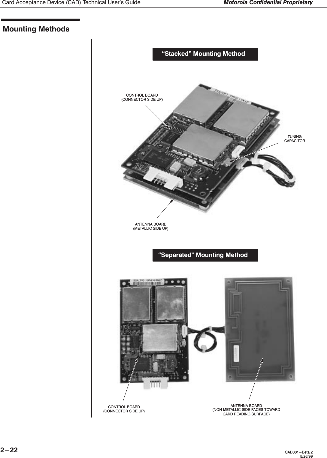
Motorola Solutions 89FT7601 Data Module User Manual
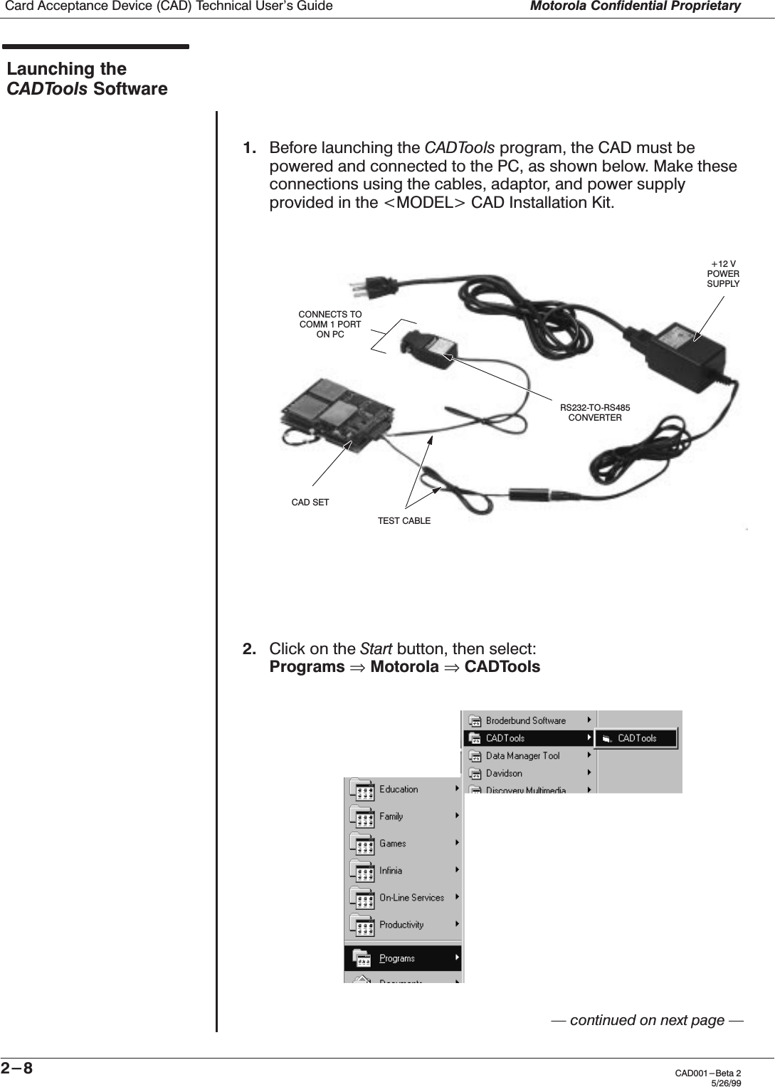
Motorola Solutions, Inc. Data Module
UserManual.wiki
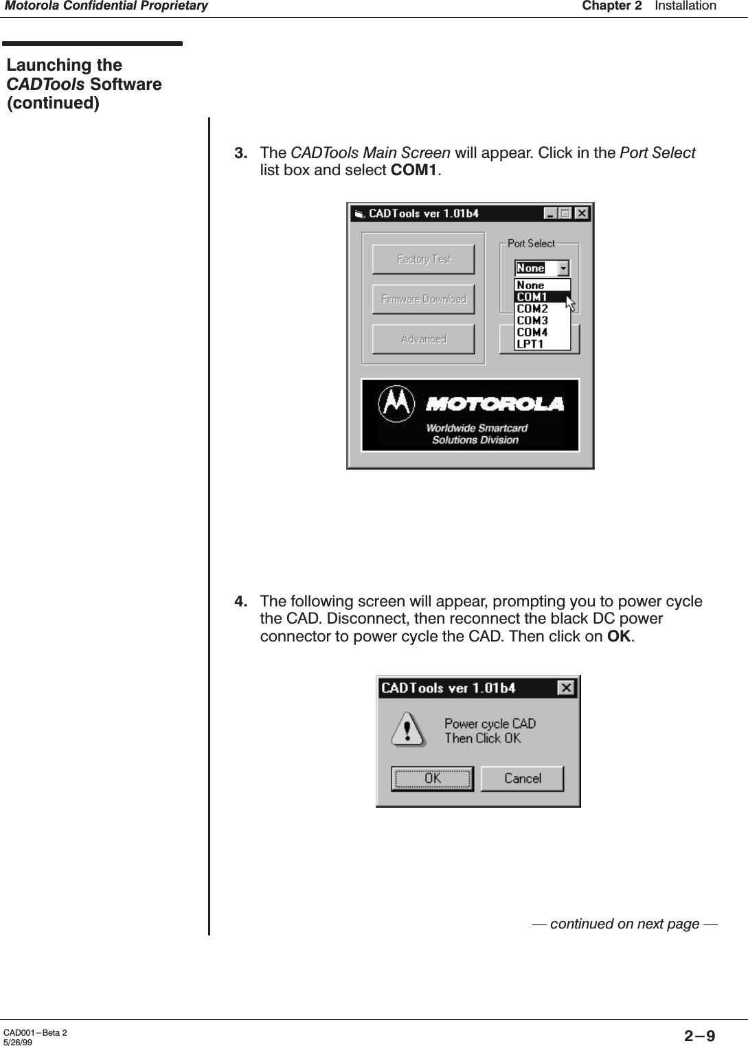
>
Motorola Solutions
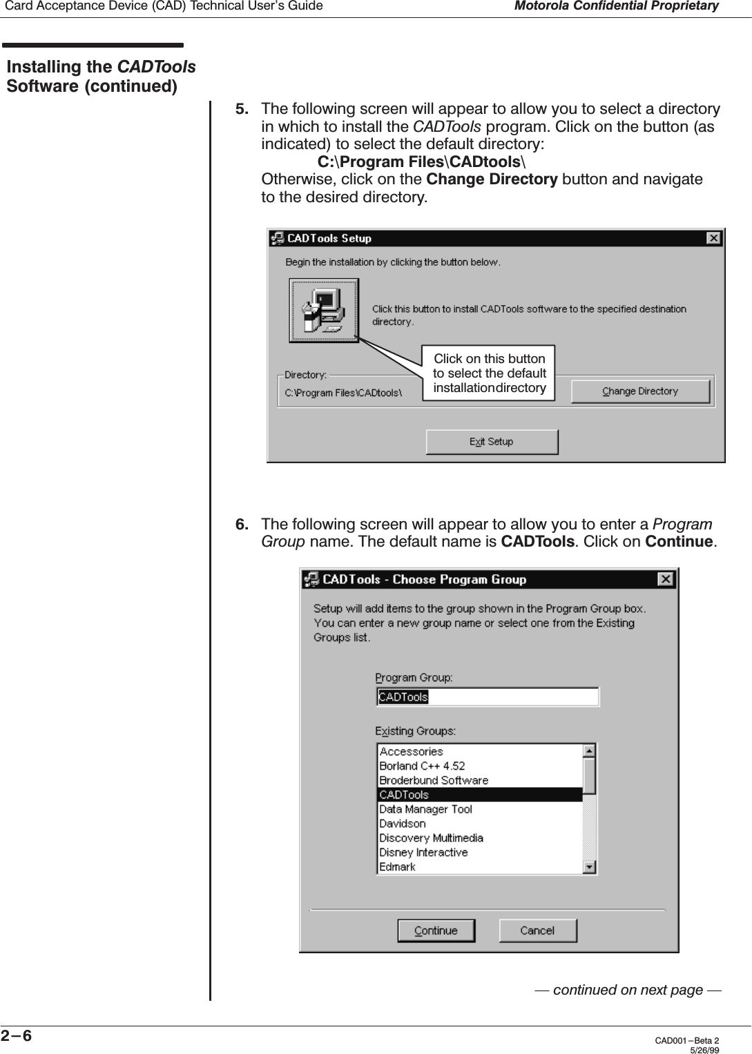
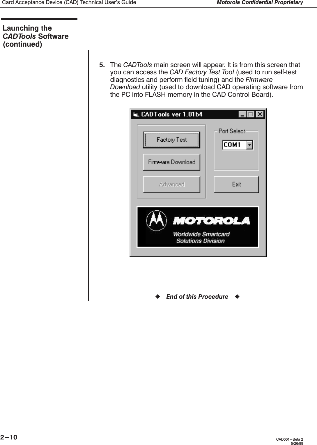
>
89FT7601 User Manual
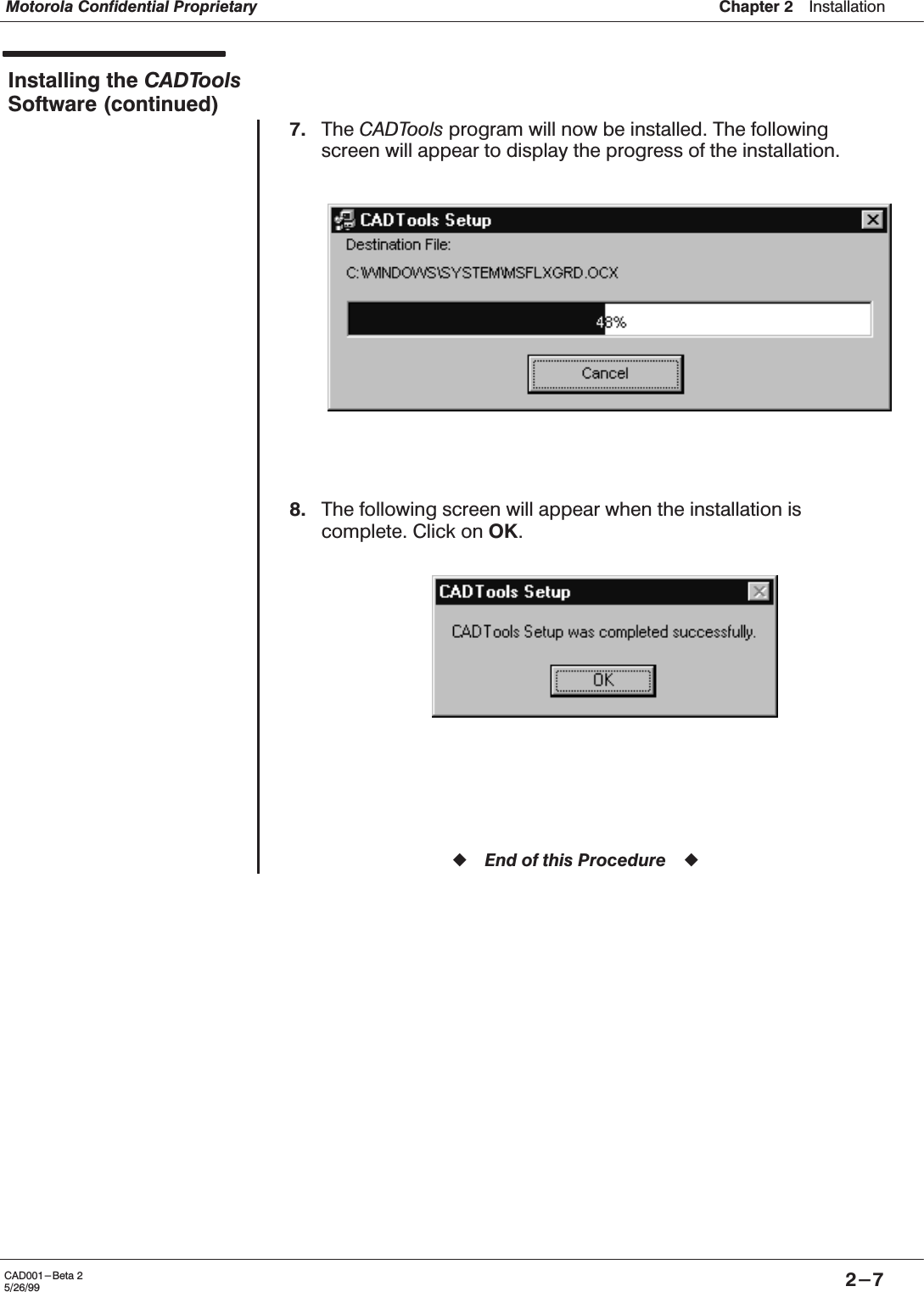
User Manual
Navigation menu
Upload a User Manual
Namespaces
Wiki Guide
HTML
PDF
Info
Views
User Manual
Discussion / Help
Navigation

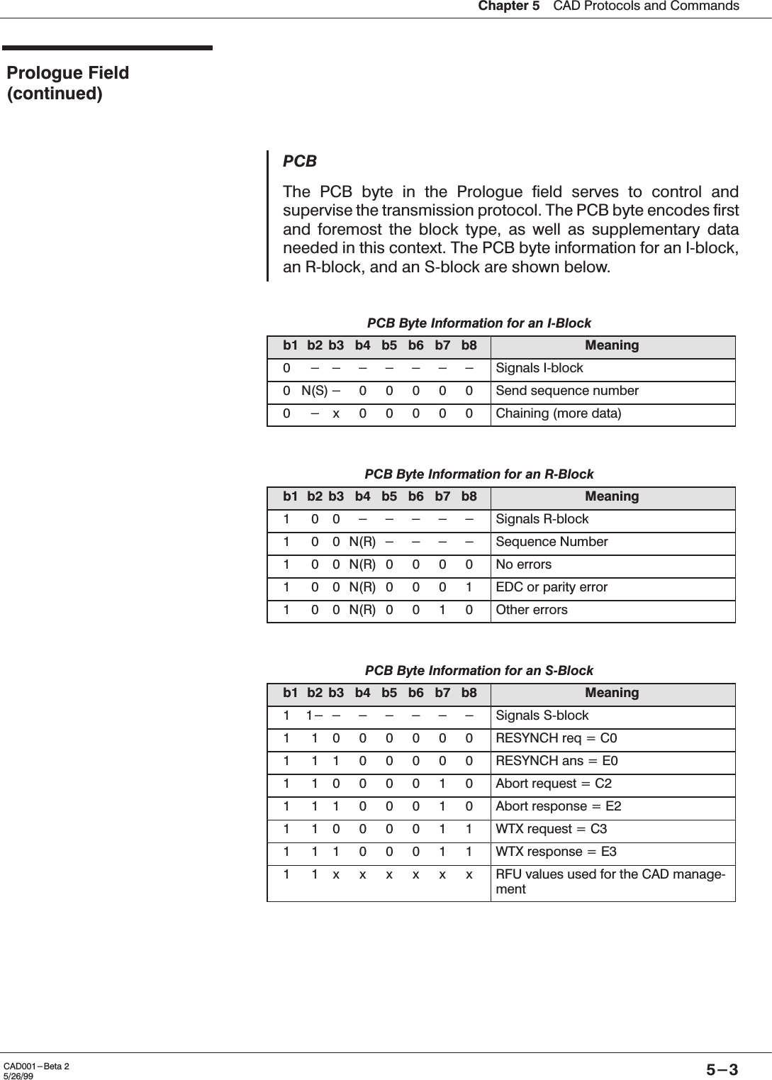
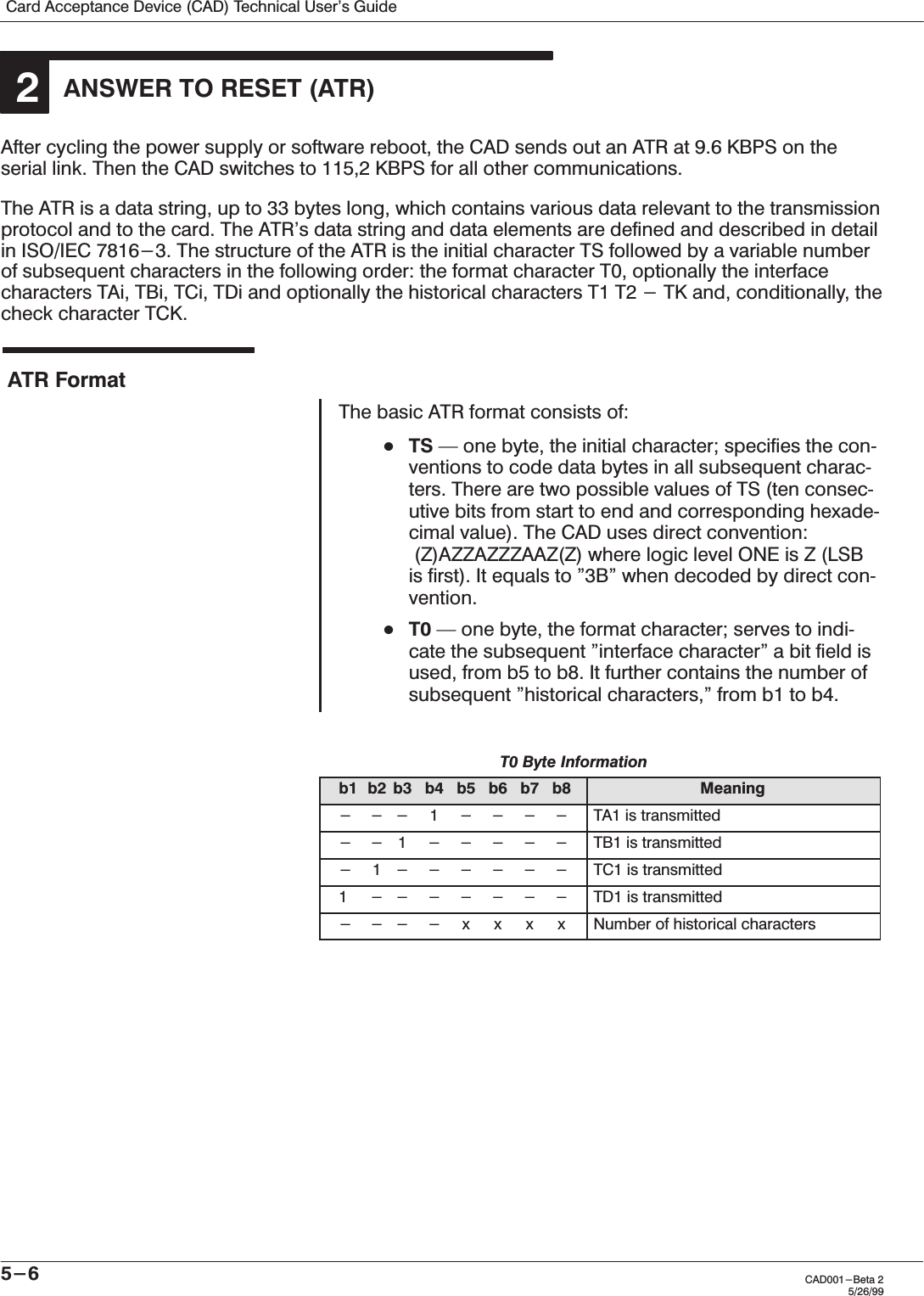
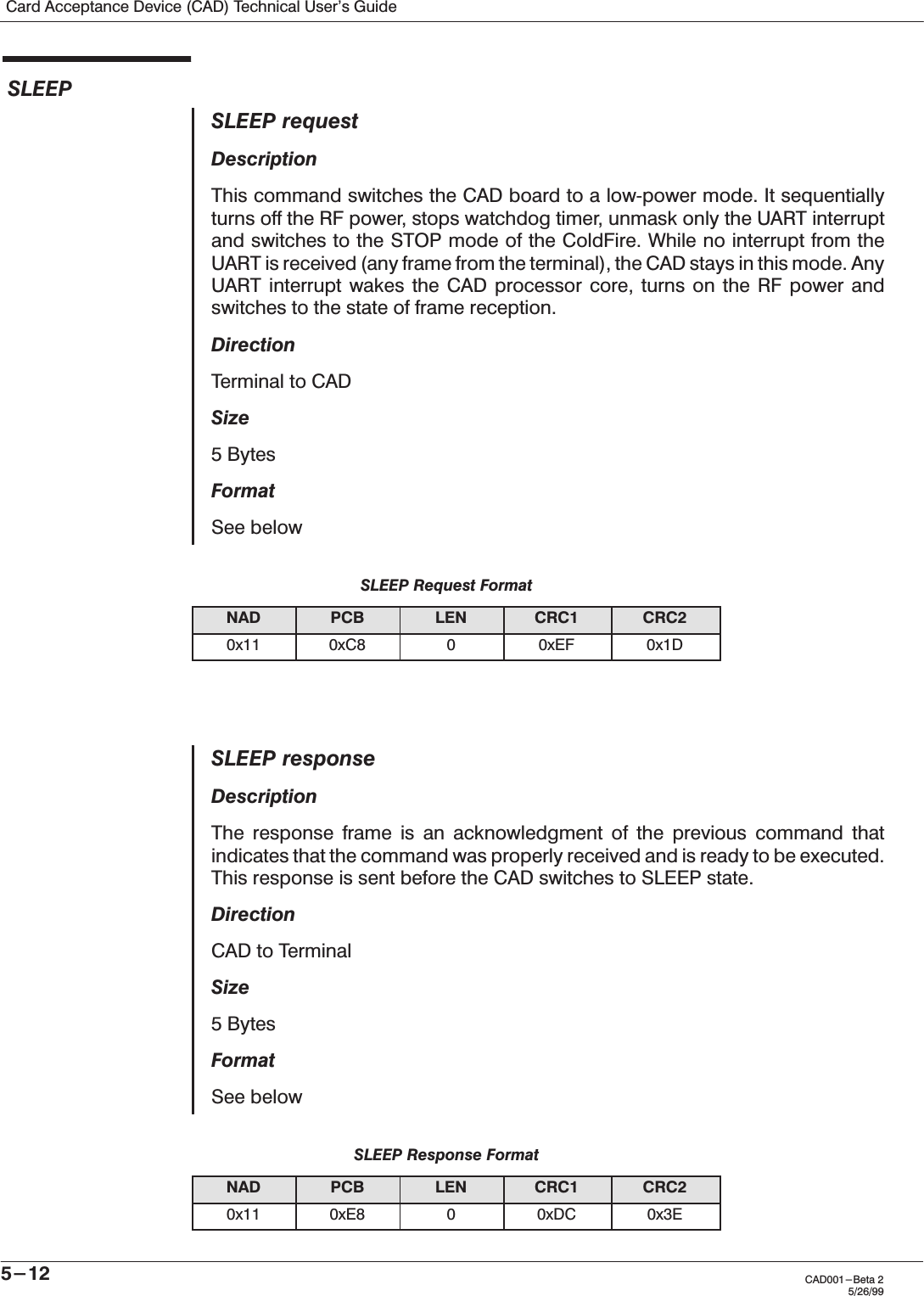
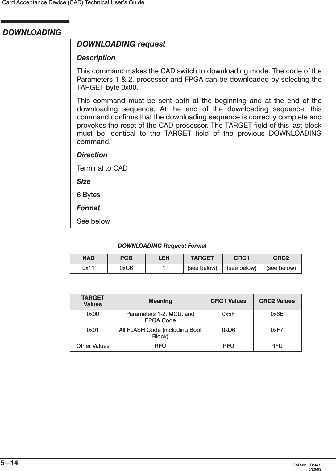
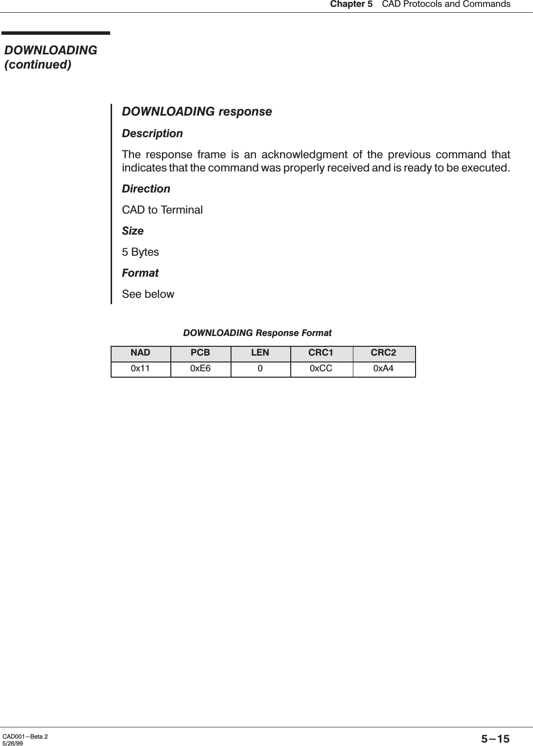
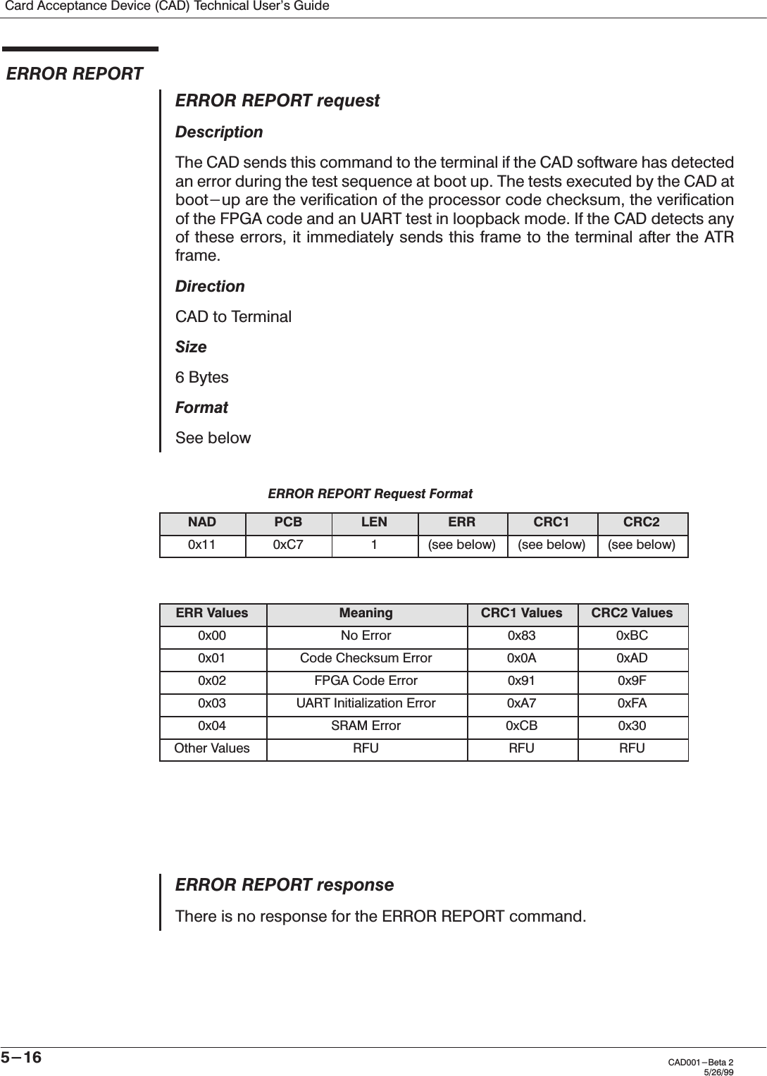
![Chapter 5ąCAD Protocols and Commands5-7CAD001-Beta 25/26/99ATR Format (continued)The four least significant bits of any interface byte TDi indicatesa protocol type T, specifying rules to be used to processtransmission protocols. When TD1 is not transmitted, T=0 isused. TA1 TB1 TC1 and TB2 are the global interface bytes. Theseglobal interface bytes shall be interpreted in order to process anytransmission protocol correctly.The interface characters specify all transmission parameters ofthe current protocol. They are constructed from the bytes TAI,TBI, TCI, and TDi (i =1, 2, 3-). TA, TBi and TCi indicate theprotocol parameters. Their interpretation depends on theprotocol type indicated by T in TDi-1. TDi indicates the protocoltype T, as defined in [1] Section 6.1.4.3, and the presence ofsubsequent interface characters. The ATR transmission of thesebytes is optional and may be omitted if appropriate.TDi Byte Informationb1 b2 b3 b4 b5 b6 b7 b8 Meaning--- 1 ---- TAi+1 is transmitted--1 ----- TBi+1 is transmitted- 1------ TCi+1 is transmitted1 ------- TDi+1 is transmitted----xxxx Protocol type for subsequent transmisĆsionWhen TDi is not transmitted, the default value of TAi+1 TBi+1TCi+1 is null, indicating that no further interface charactersTAi+1 TBi+1 TCi+1 TDi+1 will be transmitted. TA1 to TC3convey information that shall be used during exchangesbetween the terminal and the CAD subsequent to the Answer toReset. They indicate the values of the transmission controlparameters F, D, I, P, and N, and the IFSC, block waiting timeinteger (BWI), and character waiting time integer (CWI)applicable to T=1 as defined in ISO/IEC 7816-3. Theinformation contained in TA1 to TC1 and TC2 shall apply to allsubsequent exchanges.The historical characters, T1 T2 -TK, maximum 15 characters.It designates general information, for example, the CAD firmwareversion.The value of check character TCK shall be such that theexclusive-ORing of all bytes from byte T0 to the last byte beforethe TCK.](https://usermanual.wiki/Motorola-Solutions/89FT7601/User-Guide-45774-Page-59.png)