Motorola Solutions 89FT7601 Data Module User Manual
Motorola Solutions, Inc. Data Module
User Manual
CARD ACCEPTANCE DEVICE (CAD)
Technical User's Guide
CAD001-Beta 2
Motorola Confidential Proprietary
PRELIMINARY

MOTOROLA READER WARRANTY
Warranty: Motorola, Inc. (Motorola") warrants its Motorola manufactured smartcard reader or terminal (ProdĆ
uct") to the original purchaser (Buyer") as stated herein, except to the extent the terms herein may be modified by a
written SmartCard Systems Agreement between Motorola and Buyer. Smartcards are not covered by this warranty.
Motorola warrants the Product against material defects in material and workmanship under normal use and service
for a period of One (1) Year from the date of Product shipment. Motorola, at its option, will at no charge either repair
the Product (with new or reconditioned parts), replace it with the same or equivalent product (using new or recondiĆ
tioned parts), or refund the purchase price of the Product during the warranty period provided Buyer notifies MotoĆ
rola within the warranty period in accordance with the terms of this warranty. Repaired or replaced product is warĆ
ranted for the balance of the original applicable warranty period. All replaced parts of the Product shall become the
property of Motorola.
Warranty Exclusions: This warranty does NOT cover:
1. Defects, damage or malfunctions of the Product resulting from:
(a) Use of the Product in other than its normal and customary manner.
(b) Misuse, accident, neglect, environmental or site conditions not conforming to the Product specifications.
(c) Alteration, modification, adjustment, repair or testing of the Product not approved by Motorola.
(d) Equipment not approved by Motorola for use with the Product.
(e) Excessive power conducted or radiated from equipment not approved by Motorola for use with the ProdĆ
uct.
2. Product which has had the serial number removed or made illegible.
3. Normal and customary wear and tear.
4. Fraud, theft or loss resulting from unauthorized use of the Product.
5. Loss of value or data stored in the Product or in other equipment used with the Product.
6. Disclosure of personal or confidential information or data stored in or accessed by the Product.
7. Loss or damage from Product or system downtime.
8. Scratches or other cosmetic damage to Product surfaces that does not affect the operation of the Product.
9. That the software in the Product will meet the purchaser's requirements or that the operation of the software will
be uninterrupted or error-free.
General Provisions: This express warranty is extended by Motorola to the original Buyer purchasing the Product,
and is not assignable or transferable to any other party. This is the complete warranty for the Product. Motorola
assumes no obligations or liability for additions or modifications to this warranty unless made in writing and signed
by an officer of Motorola. Unless made in a separate written agreement(s) between Motorola and Buyer, Motorola
does not warrant the maintenance or service of the Products other than stated herein.
Motorola cannot be responsible in any way for any ancillary equipment not furnished by Motorola which is attached
to or used in connection with the Product, or for operation of the Product with any ancillary equipment, and all such
equipment is expressly excluded from this warranty. Because each system which may use the Product is unique,
Motorola disclaims liability for read range, transaction time, or operation of the system as a whole under this warranĆ
ty other than stated above.
This warranty sets forth the full extent of Motorola's responsibilities regarding the Product. Replacement or refund
of the purchase price, at Motorola's option, is the exclusive remedy. THIS WARRANTY IS GIVEN IN LIEU OF ALL
OTHER EXPRESS WARRANTIES. MOTOROLA DISCLAIMS ALL OTHER WARRANTIES OR CONDITIONS, EXĆ
PRESS OR IMPLIED, INCLUDING THE IMPLIED WARRANTIES OR CONDITIONS OF MERCHANTABILITY AND
FITNESS FOR A PARTICULAR PURPOSE. IN NO EVENT SHALL MOTOROLA BE LIABLE FOR DAMAGES IN EXĆ
CESS OF THE PURCHASE PRICE OF THE PRODUCT, FOR ANY LOSS OF USE, LOSS OF TIME, INCONVEĆ
NIENCE, COMMERCIAL LOSS, LOST PROFITS OR SAVINGS OR OTHER INCIDENTAL, SPECIAL, INDIRECT OR
CONSEQUENTIAL DAMAGES ARISING OUT OF THE USE OR INABILITY TO USE SUCH PRODUCT, TO THE FULL
EXTENT SUCH MAY BE DISCLAIMED BY LAW.

Patent and Software Provisions: Motorola will defend, at its own expense, any suit brought against the Buyer to
the extent that it is based on a claim that the Product or its parts infringe a United States patent, and Motorola will pay
those costs and damages finally awarded against the Buyer in any such suit which are attributable to any such
claim, but such defense and payments are conditioned on the following:
(a) that Motorola will be notified promptly in writing by Buyer of any notice of such claim;
(b) that Motorola will have sole control of the defense of such suit and all negotiations for its settlement or comproĆ
mise; and
(c) should the Product or its parts become, or in Motorola's opinion be likely to become, the subject of a claim of
infringement of a United States patent, that Buyer will permit Motorola, at its option and expense, either to
procure for Buyer the right to continue using the Product or its parts or to replace or modify the same so that it
becomes non-infringing or to grant Buyer a credit for the Product or its parts as depreciated and accept its
return. The depreciation will be an equal amount per year over the lifetime of the Product or its parts as estabĆ
lished by Motorola.
Motorola will have no liability with respect to any claim of patent infringement which is based upon the combination
of the Product or its parts furnished hereunder with software, apparatus or devices not furnished by Motorola, nor
will Motorola have any liability for the use of ancillary equipment or software not furnished by Motorola which is
attached to or used in connection with the Product. The foregoing states the entire liability of Motorola with respect
to infringement of patents by the Product or any its parts thereof.
Laws in the United States and other countries preserve for Motorola certain exclusive rights for copyrighted MotoroĆ
la software such as the exclusive rights to reproduce in copies and distribute copies of such Motorola software.
Motorola software may be used in only the Product in which the software was originally embodied and such softĆ
ware in such Product may not be replaced, copied, distributed, modified in any way, or used to produce any derivaĆ
tive thereof. No other use including, without limitation, alteration, modification, reproduction, distribution, or reĆ
verse engineering of such Motorola software or exercise of rights in such Motorola software is permitted. No license
is granted by implication, estoppel or otherwise under Motorola patent rights or copyrights.
FCC INTERFERENCE WARNING
This device complies with part 15 of the FCC Rules. Operation is subject to the following two conditions: (1) This
device may not cause harmful interference, and (2) this device must accept any interference received, including
interference that may cause undesired operation.
CAUTION:ąChanges or modifications not expressly approved by Motorola could void the user's authority to operĆ
ate the equipment.


EMotorola, Inc. 1999
All Rights Reserved
Printed in U.S.A.
CAD001-Beta 2
5/26/99
Commercial Government and
Industrial Solutions Sector
1301 E. Algonquin Road, Schaumburg, IL 60196
Commercial Government and
Industrial Solutions Sector CARD ACCEPTANCE DEVICE
(CAD)
Table of Contents
Foreword iii..........................................................................
Performance Specifications iv..........................................................
1
Description
chapter
Product Overview page 2.....................................................................
Simplified Block Diagram Theory page 4.......................................................
2
Installation
chapter
Unpacking and Inspection page 2.............................................................
Verifying Proper Operation page 4............................................................
Tuning Procedure page 14....................................................................
Installing CAD into Terminal page 20..........................................................
Final Checkout Procedure page 22............................................................
3
chapter
Troubleshooting
Fault Isolation Procedures page 2.............................................................
Returning Faulty CADs to Motorola page 3.....................................................
4
chapter
Functional Theory of Operation
Functional Theory of Operation page 2........................................................

Table of Contents Motorola Confidential Proprietary
ii 5/26/99CAD001-Beta 2
5
chapter
CAD Protocols and Commands
TerminalĆtoĆCAD Command Protocol page 2...................................................
Answer to Reset (ATR) page 6................................................................
CAD Management Commands page 8.........................................................
Command Sequences page 28................................................................
Appendix
Appendix A Ċ Performing FLASH Upgrades page A-1....................................
Appendix B Ċ CAD Connector PinĆOuts page B-1.......................................
Appendix C Ċ Dimensions and Clearances page C-1....................................
and MOTOROLA are trademarks of Motorola, Inc.
IBM is a registered trademark of International Business Machines, Inc.

Table of ContentsMotorola Confidential Proprietary
iii
5/26/99 CAD001-Beta 2
FOREWORD
Product Maintenance
Philosophy
Due to the high percentage of surfaceĆmount components and multiĆ
layer circuit board design, the maintenance philosophy for this product
is one of Field Replaceable Unit (FRU) substitution. Each Control
Board and Antenna Board matched set is considered a FRU, and when
determined to be faulty, may be quickly and easily replaced with a
known good set to bring the equipment back to normal operation. The
faulty CAD set must then be shipped to the Motorola System Support
Center for further troubleshooting and repair to the component level.
Service and
Replacement Modules
Motorola System Support Center
1311 E. Algonquin Road
Schaumburg, IL 60196
1-800-221-7144
FAX 847-576-2172
Int'l 847-576-7300
For complete information on ordering FRU replacement modules, or
instructions on how to return faulty modules for repair, contact the
Motorola System Support Center (see sidebar).
The CAD set (Control Board and Antenna Board) is considered a FRU.
If the CAD is determined to be faulty, the entire CAD must be returned
and will be repaired or replaced with a new CAD.
Scope of Manual
This manual is intended for use by experienced technicians familiar
with similar types of equipment. In keeping with the maintenance phiĆ
losophy of Field Replaceable Units (FRU), this manual contains funcĆ
tional information sufficient to give service personnel an operational
understanding of all FRU modules, allowing faulty FRU modules to be
identified and replaced with known good FRU replacements.
The information in this manual is current as of the printing date.
Changes which occur after the printing date are incorporated by InĆ
struction Manual Revisions (SMR). These SMRs are added to the manĆ
uals as the engineering changes are incorporated into the equipment.

Table of Contents Motorola Confidential Proprietary
iv 5/26/99CAD001-Beta 2
PERFORMANCE SPECIFICATIONS
Electrical
Required Supply Voltage 12 V dc +10% / -5%; ripple less than 50 mV PĆP
Required Supply Current 300 mA
Maximum Input Power Requirements 4.0 Watts
CAD PowerĆUp Time Less than 1.7 seconds after power applied
Spurious and Intentional Emissions Compliant with FCC Regulation Part 15.225
Compliant with IĆETS 300 330 clause 7.2.1.3, 7.4.3.2, 7.4.4.2
Environmental
Operating Temperature 0_Cto70_C; Compliant with IEC 68Ć2Ć2 Part 2 Test Bd and IEC 68Ć2Ć1 Part 2
Test Ad, with duration of 16 hours
Storage Temperature -40_Cto85_C; Compliant with IEC 68Ć2Ć2 Part 2 Test Bb and IEC 68Ć2Ć1 Part
2 Test Ab, with duration of 72 hours
Humidity
Operating: 5% to 95% nonĆcondensing
Compliant with IEC 68Ć2Ć3 Part 2 Test Ca, with duration of 4 days; high humidity
test only
Cold and Heat Shock
Compliant with IEC 68Ć2Ć1 Part 2 Test Aa, with temperature -40_Candduration
of 2 hours, and IEC 68Ć2Ć2 Part 2 Test Ba, with temperature 85_C and duration
of 2 hours
Vibration
Compliant with IEC 68Ć2Ć6 with the following parameters:
Frequency Range:ą10 Hz to 500 Hz
Vibration Severity:ą3 gn
Sweep Rate:ą1 octave per minute
Endurance by Sweeping:ą20 sweep cycles for each X, Y, and Z axis
Critical Frequency Duration:ą10 million cycles or 10 hours at the fundamental
resonant frequency
Shock Compliant with IEC 68Ć2Ć27 Part 2 Test Ea; severity 60 gn; duration 11 msec
Bump Compliant with IEC68Ć2Ć29 Part 2 Test Eb; severity 40 gn; duration 6 msec; numĆ
ber of bumps: 4000
Electrostatic Discharge Compliant with IEC 801Ć2, Severity Level 4
Electromagnetic Fields Compliant with ISO 10536Ć1, 4.2.8
Transmitter
Frequency 13.56 MHz .01%
Maximum Output Coil Current 1.00 App
Modulation Rise and Fall Time <2.0 msec
ASK Modulation 8% 14%
Receiver
Carrier Frequency 13.56 MHz
Subcarrier Frequency 847.5 kHz
Subcarrier Data NRZĆL BPSK (ISO Type B)

Table of ContentsMotorola Confidential Proprietary
v
5/26/99 CAD001-Beta 2
Operational
CADĆtoĆTerminal Communication Rates
115,200 bps (default)
57,600 bps
38,400 bps
19,200 bps
9,600 bps
CADĆtoĆCard Communication Rates 105.9375 Kbps
CADĆtoĆCard Operating Radio Frequency 13.56 MHz
ISO Card Type Type B

Table of Contents Motorola Confidential Proprietary
vi 5/26/99CAD001-Beta 2
Notes...

Chapter 1 "Description
Card Acceptance Device (CAD)
Technical User's Guide
CAD001-Beta 2
5/26/99
chapter contents
Product Overview 2
Simplified Block Diagram Theory 4

Card Acceptance Device (CAD) Technical User's Guide
1-2 CAD001-Beta 2
5/26/99
1PRODUCT OVERVIEW
The Motorola Card Acceptance Device (CAD) is an electronic module capable of communicating with
ISO 1443 Type BĆcompatible smart cards via an radio frequency (RF) interface. This section provides
general information about the application and physical properties of the CAD.
Physical Description
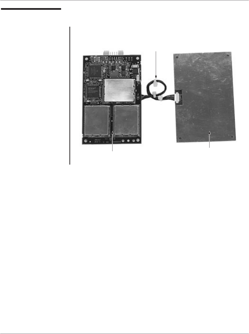
Overview
The CAD, which provides the communications interface between a
terminal and customer smart cards, consists of a Control Board and
an Antenna Board. These two boards are connected together by a
100 mm multiĆconductor interconnect cable. The CAD is connected
to the terminal via a 10Ćpin connector located on the Control Board.
Control Board
The Control Board contains a microprocessor, nonĆvolatile memory,
and radio frequency transmitting and receiving circuitry. This board
communicates with smart cards via an RF link (provided by the
Antenna Board), and to the terminal via RS485 serial protocol.
Antenna Board
The Antenna Board consists of printed circuit board with copper
traces forming the transmit and receive antenna. The board is
attached to a ferrite plate and a metal back plate that serves as a
ground plane.
Typical Application
The CAD described in this manual is specifically designed to
operate in AES Prodata Automated Fare Collection Terminals for the
purpose of allowing customers to electronically pay fares on mass
transit vehicles.
Chapter 1ąDescription
1-3
CAD001-Beta 2
5/26/99
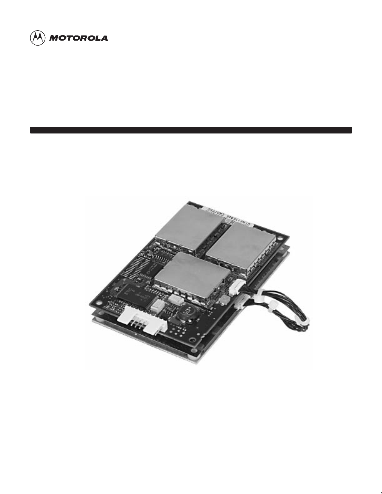
CAD Primary
Components
ANTENNA BOARD
CONTROL BOARD
INTERCONNECT
CABLE
CONNECTS TO
CABLE FROM TERMINAL
(RS485 PROTOCOL)

Card Acceptance Device (CAD) Technical User's Guide
1-4 CAD001-Beta 2
5/26/99
2SIMPLIFIED BLOCK DIAGRAM THEORY
The illustration on the facing page shows a simplified block diagram of the CAD. This section is
intended to provide a basic understanding of the CAD circuitry and how it interacts with the terminal
and smart cards. (Refer to Chapter 4 for a more detailed block diagram and circuit descriptions.)
Overview of CAD
Operation
The CAD serves as the data communications link between
customer smart cards and the terminal in which the CAD is
installed.
For CADĆtoĆCard communications, the Control Board receives data
signals from the terminal. It then transmits these data signals via RF
to a smart card held within reading distance of the CAD's Antenna
Board.
For CardĆtoĆCAD communications, encrypted RF data signals from
the smart card are received by the Control Board (via the Antenna
Board) where they are sent to the terminal via the RS485 connector
located on the board.
Chapter 1ąDescription
1-5
CAD001-Beta 2
5/26/99
CAD Simplified Block
Diagram
CARD ACCEPTANCE DEVICE (CAD)
MICROPROCESSOR
TERMINAL
NONĆVOLATILE
MEMORY
ANALOG
(AFE)
POWER SUPPLY
CIRCUITRY
FRONT END
CONTROL BOARD
ANTENNA BOARD
RS485
DATA CABLE
+5V
+5V_A
100 MM INTERCONNECT CABLE
SMART CARD

Card Acceptance Device (CAD) Technical User's Guide
1-6 CAD001-Beta 2
5/26/99
CAD Detailed
Components
The Control Board contains components on both sides of the circuit
board. The Antenna Board contains no components, but rather
printed circuit traces which form the antenna. Refer to the photos
on the facing page for identification of the components on the two
boards.
Chapter 1ąDescription
1-7
CAD001-Beta 2
5/26/99
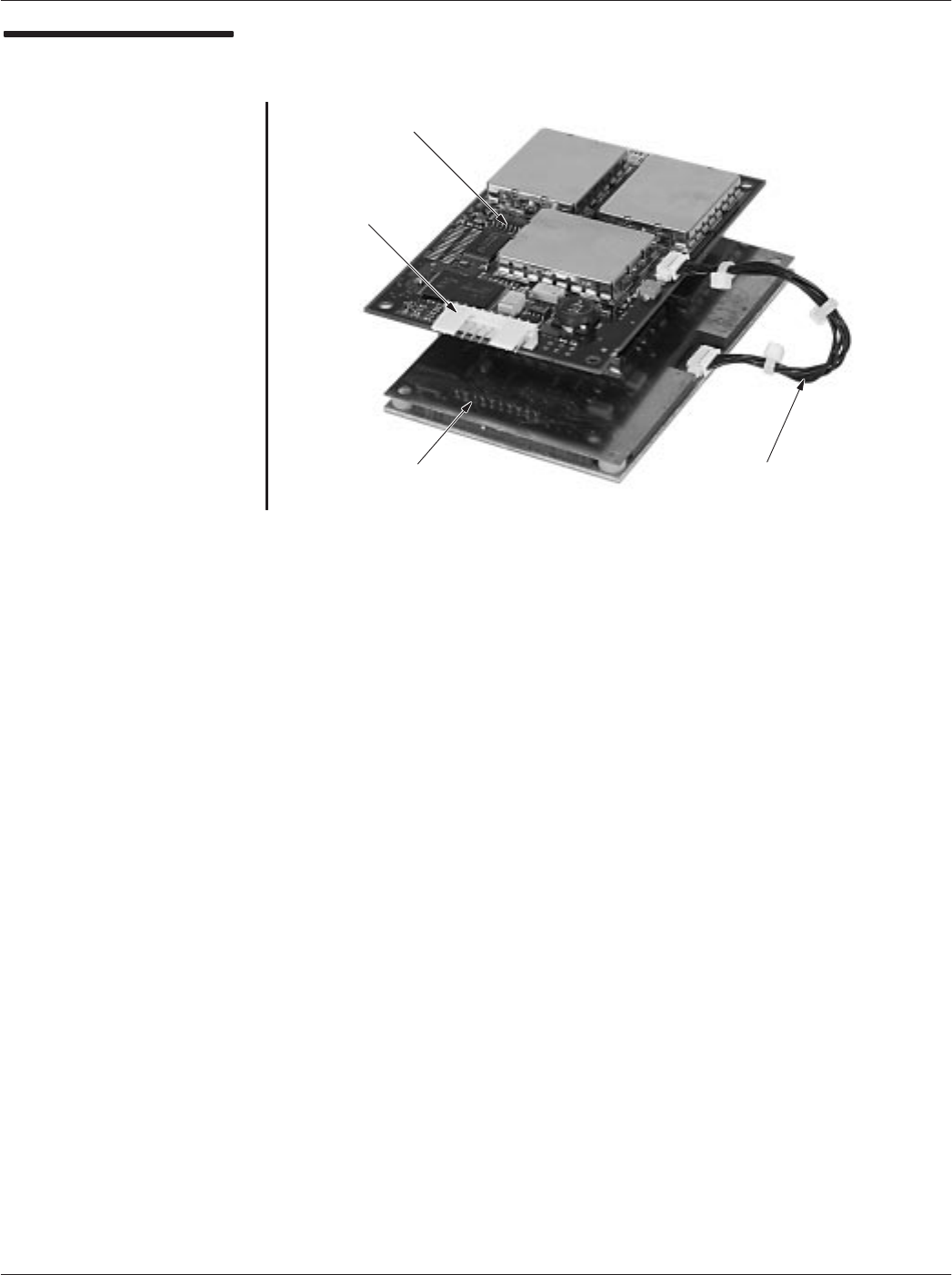
CAD Detailed
Components
SRAM
MEMORY
FLASH
MEMORY
CONTROL BOARD ANTENNA BOARD
RS485
CONNECTOR
TO/FROM
TERMINAL
TUNING
CAPACITOR
MICROPROCESSOR
METAL BACK PLATE
(GROUND PLANE)
CONTROL BOARD ANTENNA BOARD
INTERCONNECT
CABLE
ANTENNA CIRCUIT BOARD
(TRACES FORM ANTENNA)
STATUS
LED
(GREEN)
p/o
ANALOG FRONT END (AFE)
p/o
ANALOG
FRONT END
(AFE)

Card Acceptance Device (CAD) Technical User's Guide
1-8 CAD001-Beta 2
5/26/99
Notes...

Chapter 2 "Installation
Card Acceptance Device (CAD)
Technical User's Guide
CAD001-Beta 2
5/26/99
chapter contents
Unpacking and Inspection 2
Verifying Proper Operation 4
Tuning Procedure 14
Installing CAD Into Terminal 20
Final Checkout Procedure 22

Card Acceptance Device (CAD) Technical User's Guide Motorola Confidential Proprietary
2-2 CAD001-Beta 2
5/26/99
UNPACKING AND INSPECTION
1
This section describes the procedures necessary to unpack and take inventory, run a Self Test utility to
verify proper electrical operation, perform a tuning procedure, mechanically install the CAD set into an
external terminal enclosure, and perform a final checkout procedure.
Important!ąThe CAD Control Board contains CĆMOS and other staticĆsensitive components. When
handling the CAD, be sure to observe all precautions to prevent damage to the components from static
electricity. These include the use of a grounded antiĆstatic wrist strap and antiĆstatic mats and work
surfaces.
Unpacking and
Inspecting the CAD
Sets
Each CAD set (consisting of a Control Board and an Antenna Board) is
tuned and tested at the factory prior to shipment. Each CAD set is
shipped with a 10mm multiĆconductor interconnect cable connected
between the Control Board and the Antenna Board, ensuring that the
matched set remains together.
Remove each CAD set from the foam packing material and inspect for
visual damage. Report the extent of any damage to the transportation
company. Be sure to keep the cable in place to ensure that each
matched CAD sets remains together.
Chapter 2ąInstallationMotorola Confidential Proprietary
2-3
CAD001-Beta 2
5/26/99
CAD Set Connected by
Cable
ANTENNA
BOARD
CONTROL BOARD
MULTIĆCONDUCTOR
INTERCONNECT
CABLE
Card Acceptance Device (CAD) Technical User's Guide Motorola Confidential Proprietary
2-4 CAD001-Beta 2
5/26/99
VERIFYING PROPER OPERATION
2
Although each CAD set is tested at the factory before shipment, it is recommended that the AutoĆTest
utility be run on each CAD set prior to installation into a terminal. This ensures that the CAD set is
electrically functional and was not electrically damaged in transit or during unpacking.
The AutoĆTest utility is part of the CADTools program included with the <KIT NUMBER> CAD Installation
Kit (available from Motorola). The CADTools program is a Microsoft Windows compatible program that
includes a suite of factory test utilities and a firmware download utility for updating the CAD operating
software.
Required Equipment
The following hardware and software is required in order to run the Self
Test Utility on a CAD set.
D<Kit Number> CAD Installation Kit (includes Test Cable with
RS232ĆtoĆRS485 Adaptor, Power Supply, ISO Antenna Board, and
CADTools Software.
DIBM PCorIBMĆcompatible desktop or laptop computer (need
exact specs, OS version, processor type and speed, etc.)
Installing the CADTools
Software
The CADTools software is provided on two 3½" high density diskettes.
Install the software by performing the following procedure.
1. Insert the diskette labeled Disk 1 into the floppy drive of the PC.
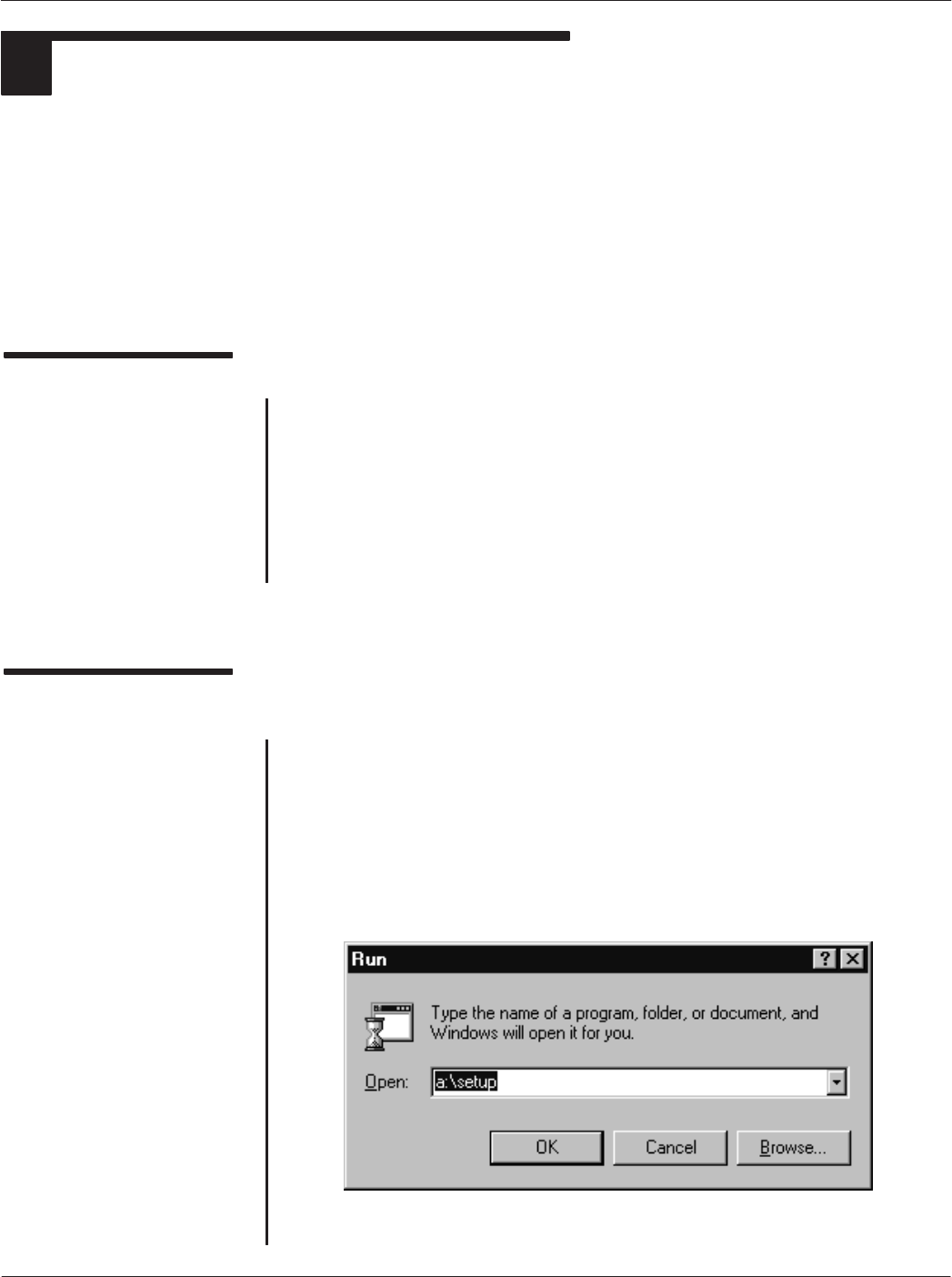
2. Click on the Start button, then Programs ⇒Run. The following
screen will be displayed. In the Open box, type a:setup and click
on OK.
Ċ continued on next page Ċ
Chapter 2ąInstallationMotorola Confidential Proprietary
2-5
CAD001-Beta 2
5/26/99
Installing the CADTools
Software (continued)
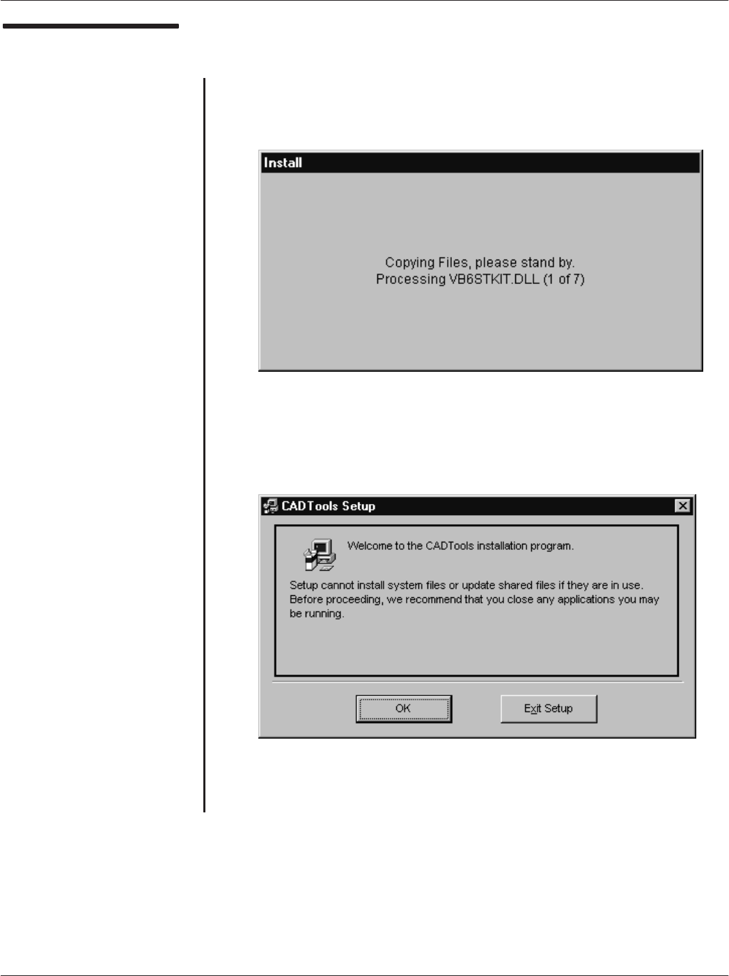
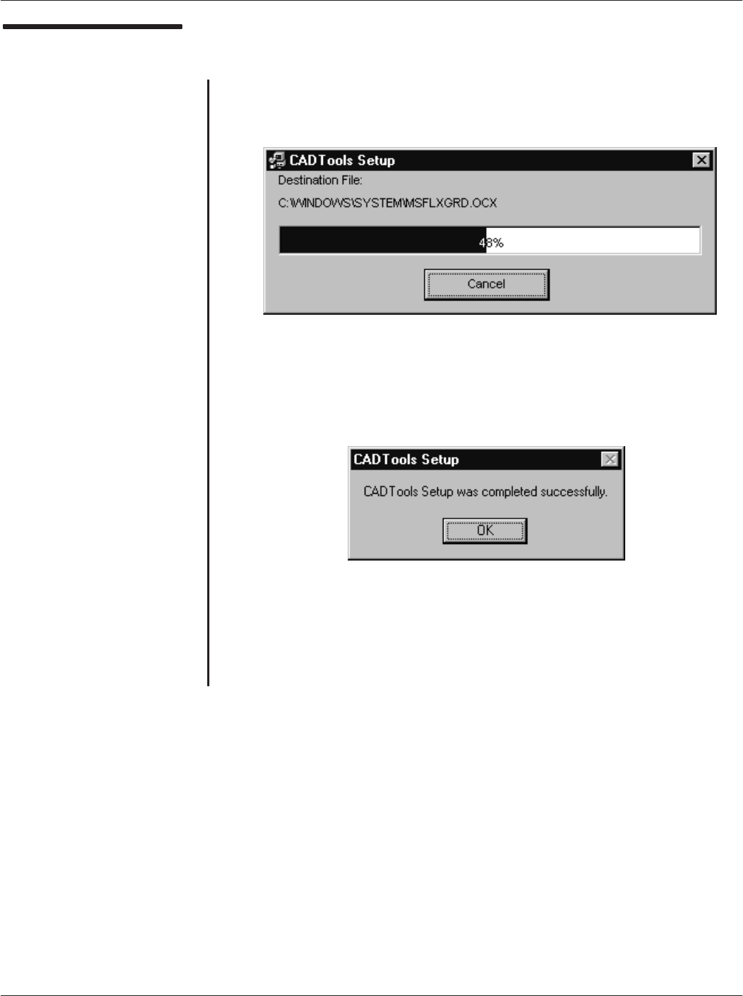
3. The installation program will now install seven system files
required by the CADTools program. The following screen
displays which files are being installed.
4. When the system files have been installed, the following
CADTools Setup screen will appear. Click on OK.
Ċ continued on next page Ċ
Card Acceptance Device (CAD) Technical User's Guide Motorola Confidential Proprietary
2-6 CAD001-Beta 2
5/26/99
Installing the CADTools
Software (continued)
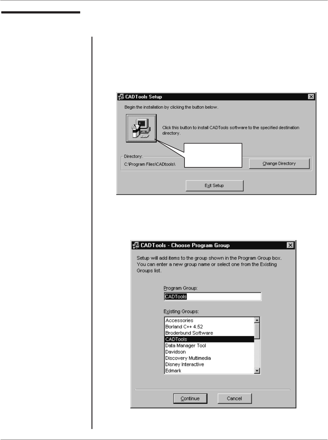
5. The following screen will appear to allow you to select a directory
in which to install the CADTools program. Click on the button (as
indicated) to select the default directory:
C:\Program Files\CADtools\
Otherwise, click on the Change Directory button and navigate
to the desired directory.
6. The following screen will appear to allow you to enter a Program
Group name. The default name is CADTools. Click on Continue.
Ċ continued on next page Ċ
Click on this button
to select the default
installationdirectory
Chapter 2ąInstallationMotorola Confidential Proprietary
2-7
CAD001-Beta 2
5/26/99
Installing the CADTools
Software (continued)
7. The CADTools program will now be installed. The following
screen will appear to display the progress of the installation.
8. The following screen will appear when the installation is
complete. Click on OK.
ząEnd of this Procedureąz
Card Acceptance Device (CAD) Technical User's Guide Motorola Confidential Proprietary
2-8 CAD001-Beta 2
5/26/99
Launching the
CADTools Software
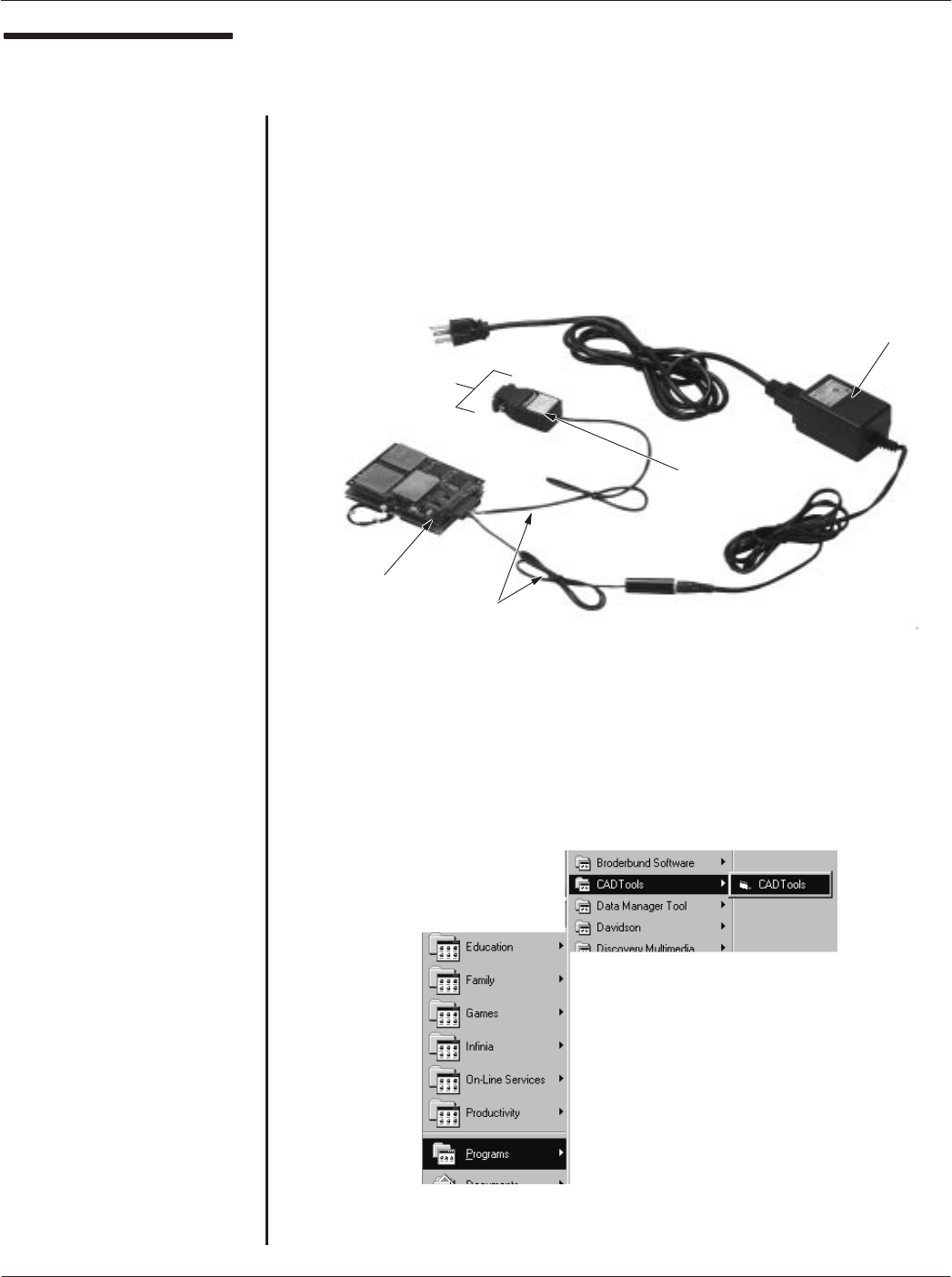
1. Before launching the CADTools program, the CAD must be
powered and connected to the PC, as shown below. Make these
connections using the cables, adaptor, and power supply
provided in the <MODEL> CAD Installation Kit.
2. Click on the Start button, then select:
Programs ⇒Motorola ⇒CADTools
Ċ continued on next page Ċ
+12 V
POWER
SUPPLY
RS232ĆTOĆRS485
CONVERTER
CAD SET
TEST CABLE
CONNECTS TO
COMM 1 PORT
ON PC
Chapter 2ąInstallationMotorola Confidential Proprietary
2-9
CAD001-Beta 2
5/26/99
Launching the
CADTools Software
(continued)
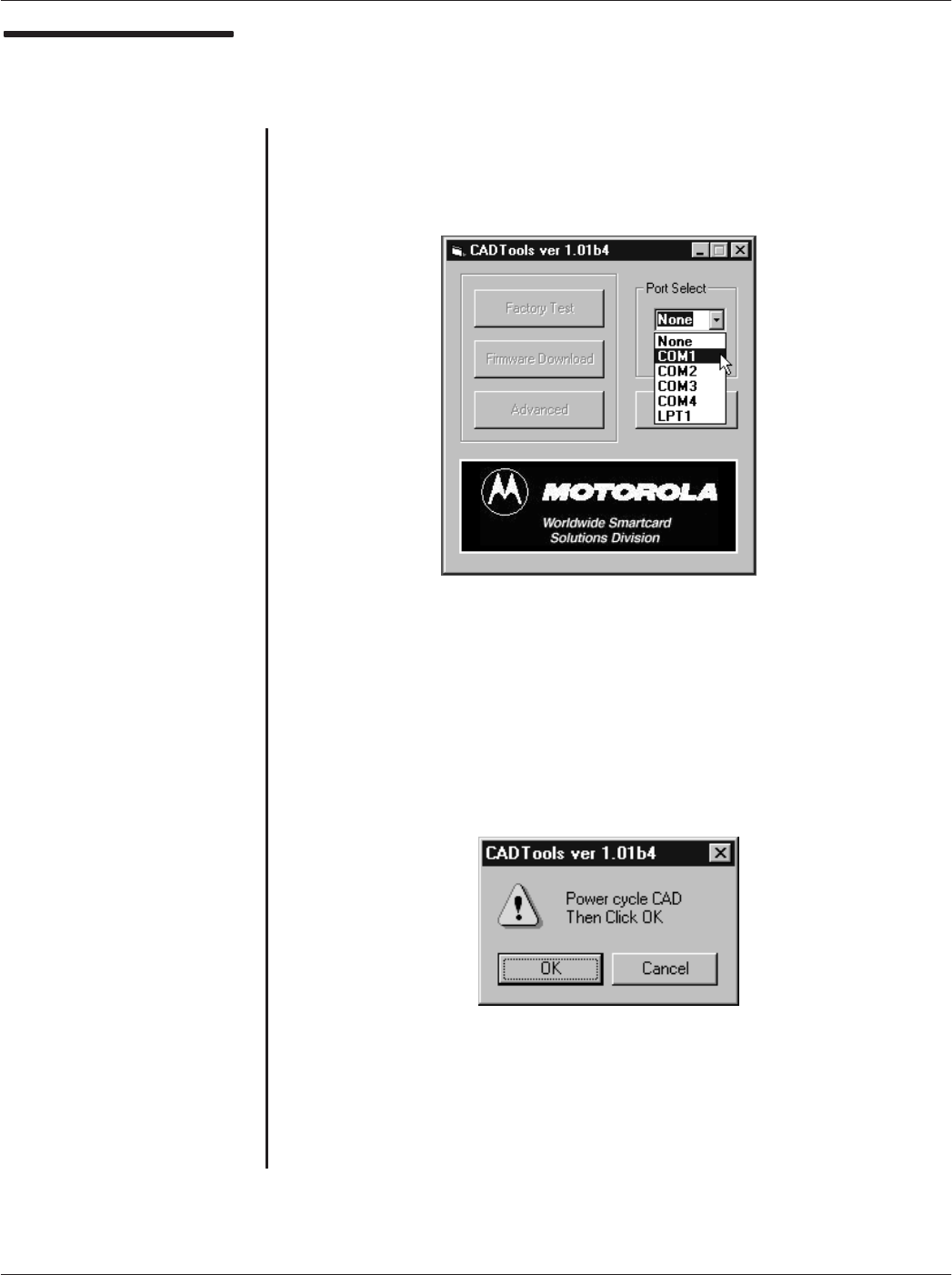
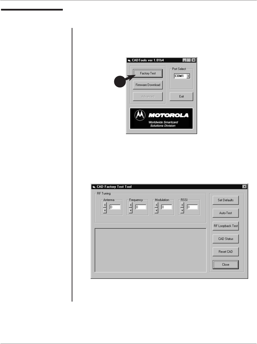
3. The CADTools Main Screen will appear. Click in the Port Select
list box and select COM1.
4. The following screen will appear, prompting you to power cycle
the CAD. Disconnect, then reconnect the black DC power
connector to power cycle the CAD. Then click on OK.
Ċ continued on next page Ċ
Card Acceptance Device (CAD) Technical User's Guide Motorola Confidential Proprietary
2-10 CAD001-Beta 2
5/26/99
Launching the
CADTools Software
(continued)
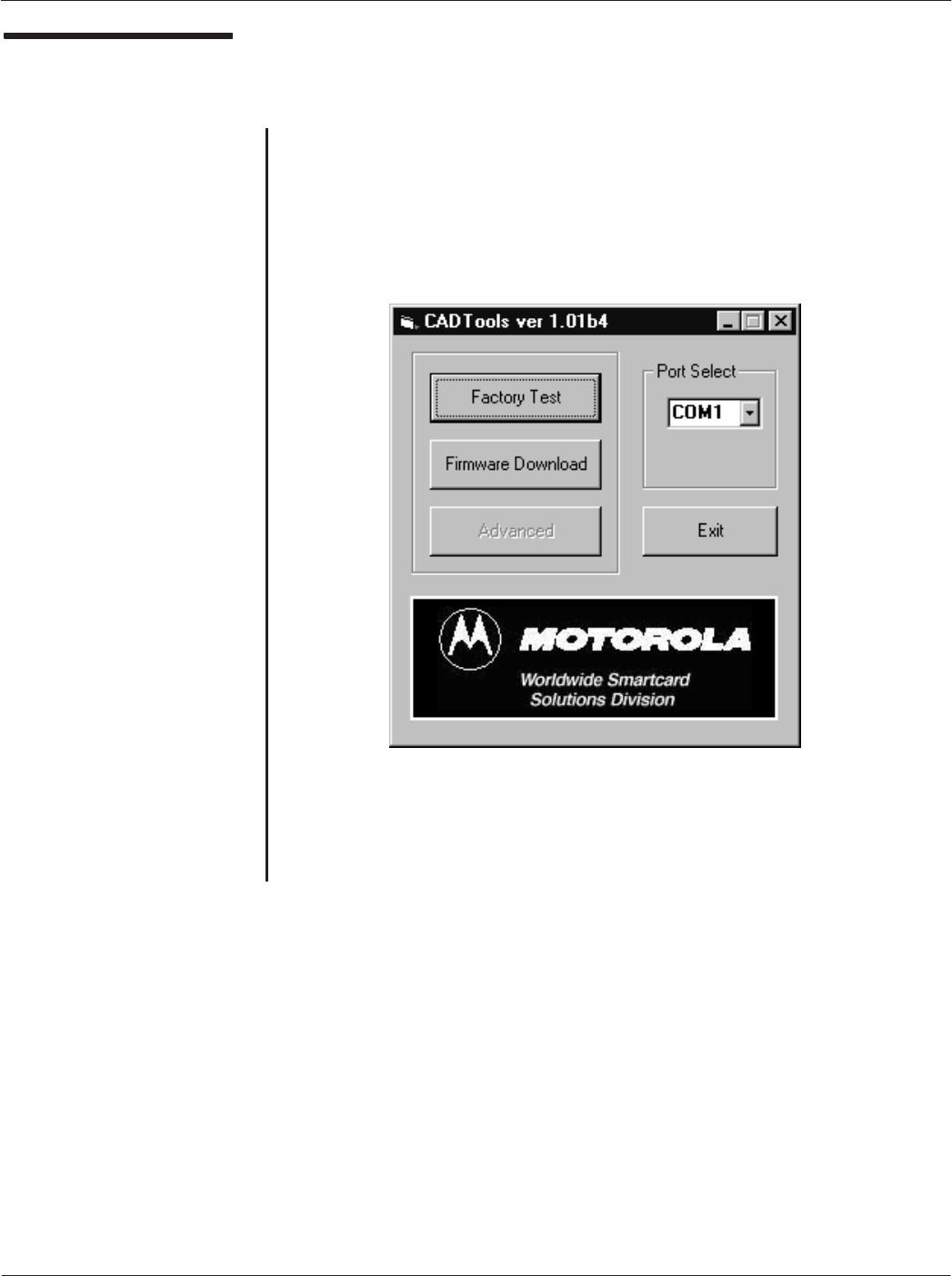
5. The CADTools main screen will appear. It is from this screen that
you can access the CAD Factory Test Tool (used to run selfĆtest
diagnostics and perform field tuning) and the Firmware
Download utility (used to download CAD operating software from
the PC into FLASH memory in the CAD Control Board).
ząEnd of this Procedureąz

Chapter 2ąInstallationMotorola Confidential Proprietary
2-11
CAD001-Beta 2
5/26/99
THIS PAGE INTENTIONALLY LEFT BLANK
Card Acceptance Device (CAD) Technical User's Guide Motorola Confidential Proprietary
2-12 CAD001-Beta 2
5/26/99
Running the SelfĆTest
Utility
1. With the CAD connected to the PC and the CADTools program
running (refer to Launching the CADTools Software on page 2-8),
click on the Factory Test button.
2. The following CAD Factory Test Tool main screen will appear.
continued on next page
1
Chapter 2ąInstallationMotorola Confidential Proprietary
2-13
CAD001-Beta 2
5/26/99
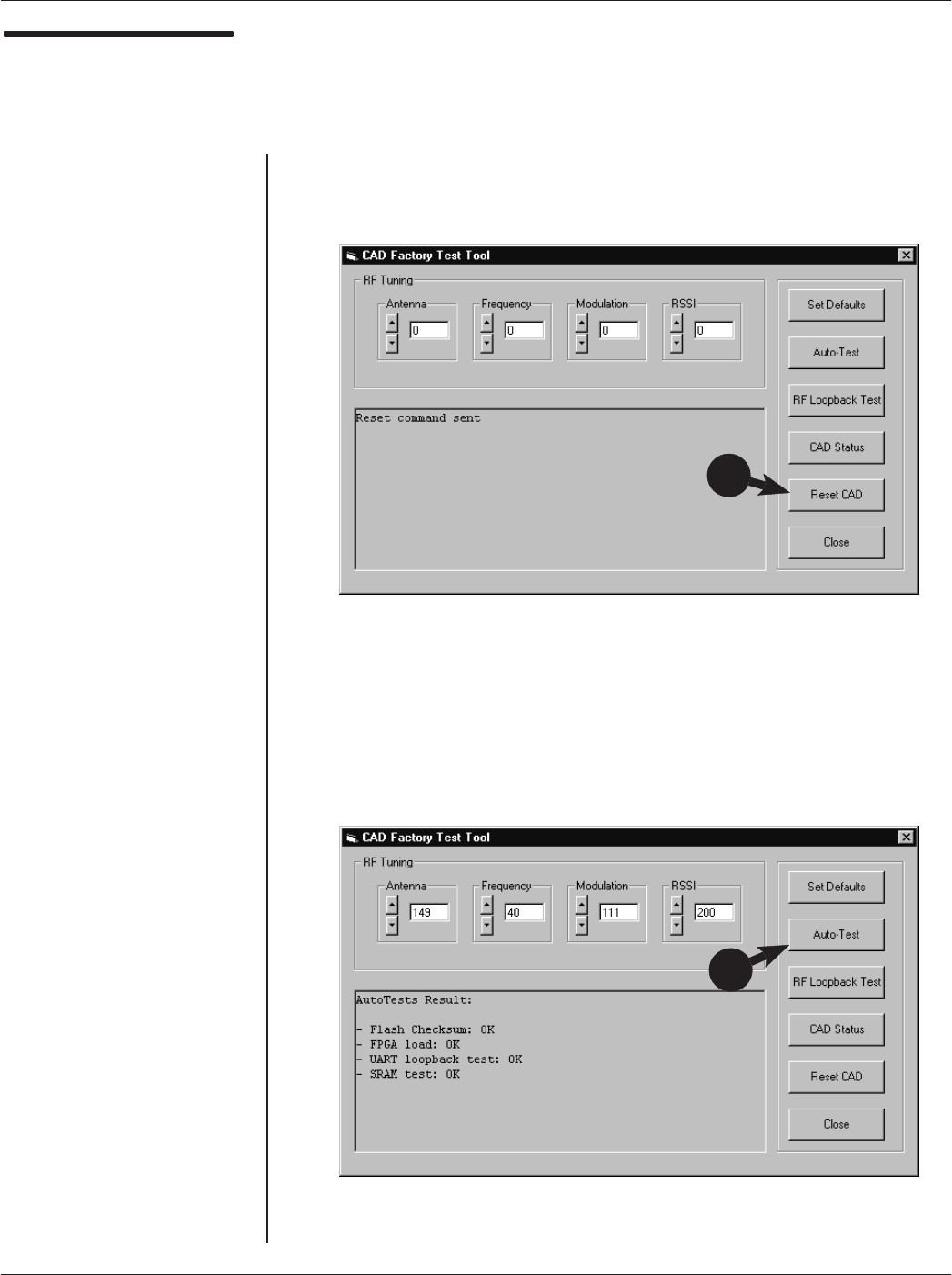
Running the Self Test
Utility
(Continued)
3. Click on the Reset CAD button to cause the CAD set to perform
a reboot process. When complete, Reset command sent will be
displayed.
4. Click on the AutoĆTest button to initiate the selfĆtest routine. The
results will be displayed as shown below. Verify that all test
results are OK.
ząEnd of this Procedureąz
3
4

Card Acceptance Device (CAD) Technical User's Guide Motorola Confidential Proprietary
2-14 CAD001-Beta 2
5/26/99
TUNING PROCEDURE
3
Although each CAD set is tuned at the factory, it is recommended that the tuning procedure be repeated before
installing the CAD into the terminal. This ensures that the CAD's read range and reliability are optimized.
NoteąTo perform the tuning procedure, you will use the CADTools program. This software application
was used previously to perform the SelfĆTest utility to verify that the CAD is electrically functional. Refer
to page 2-4 for instructions on installing this software application on your PC.
Required Equipment
The following hardware and software is required in order to run the Self
Test Utility on a CAD set.
D<Kit Number> CAD Installation Kit (includes Test Cable, Power
Supply, RS232ĆtoĆRS485 Adaptor, ISO Antenna Board, and
CADTools Software.
DIBM PC or IBMĆcompatible desktop or laptop computer (need
exact specs, OS version, processor type and speed, etc.)
DOscilloscope (Tek TDS420A, or equivalent)
DFrequency Counter (HP 53132A, or equivalent)
Chapter 2ąInstallationMotorola Confidential Proprietary
2-15
CAD001-Beta 2
5/26/99
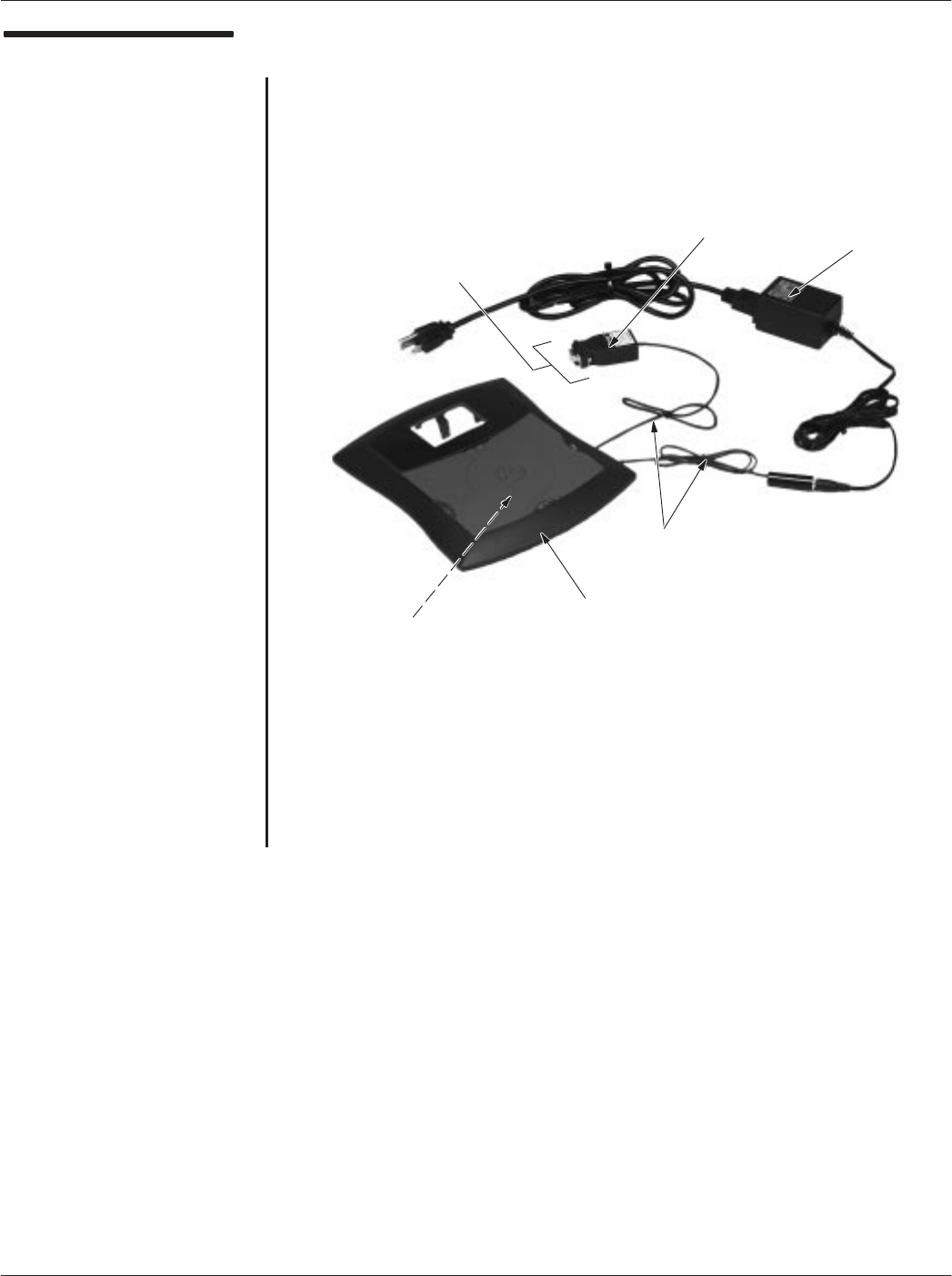
Tuning the CAD
1. Connect the CAD, PC, and power supply as shown below. Note
that the CAD is mounted in the appropriate card reader panel
for the type of terminal in which the CAD will be used.
continued on next page
+12 V
POWER
SUPPLY
RS232ĆTOĆRS485
CONVERTER
CAD SET
(INSTALLED UNDER
PANEL)
TEST CABLE
CONNECTS TO
COMM 1 PORT
ON PC
TYPICAL
READER
PANEL
Card Acceptance Device (CAD) Technical User's Guide Motorola Confidential Proprietary
2-16 CAD001-Beta 2
5/26/99
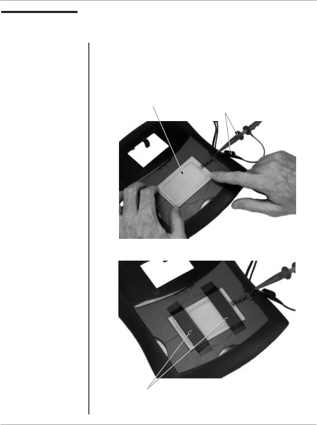
Tuning the CAD
(continued)
2. Attach the scope probe to the ISO antenna wires and position
the antenna on the reader panel (over the CAD set). While
monitoring the waveform on the oscilloscope, move the antenna
around until you achieve the maximum Vpp reading
(approximately 5 to 10 Vpp). Secure the ISO Antenna in place
using electrical tape or equivalent.
Ċ continued on next page Ċ
ISO ANTENNA SCOPE PROBE
CONNECTED TO
OSCILLOSCOPE
SECURE ANTENNA
USING TAPE
Chapter 2ąInstallationMotorola Confidential Proprietary
2-17
CAD001-Beta 2
5/26/99
Tuning the CAD
(continued)
3. Launch the CADTool program (described on page 2-8) and
click on the Factory Test button to access the CAD Factory Test
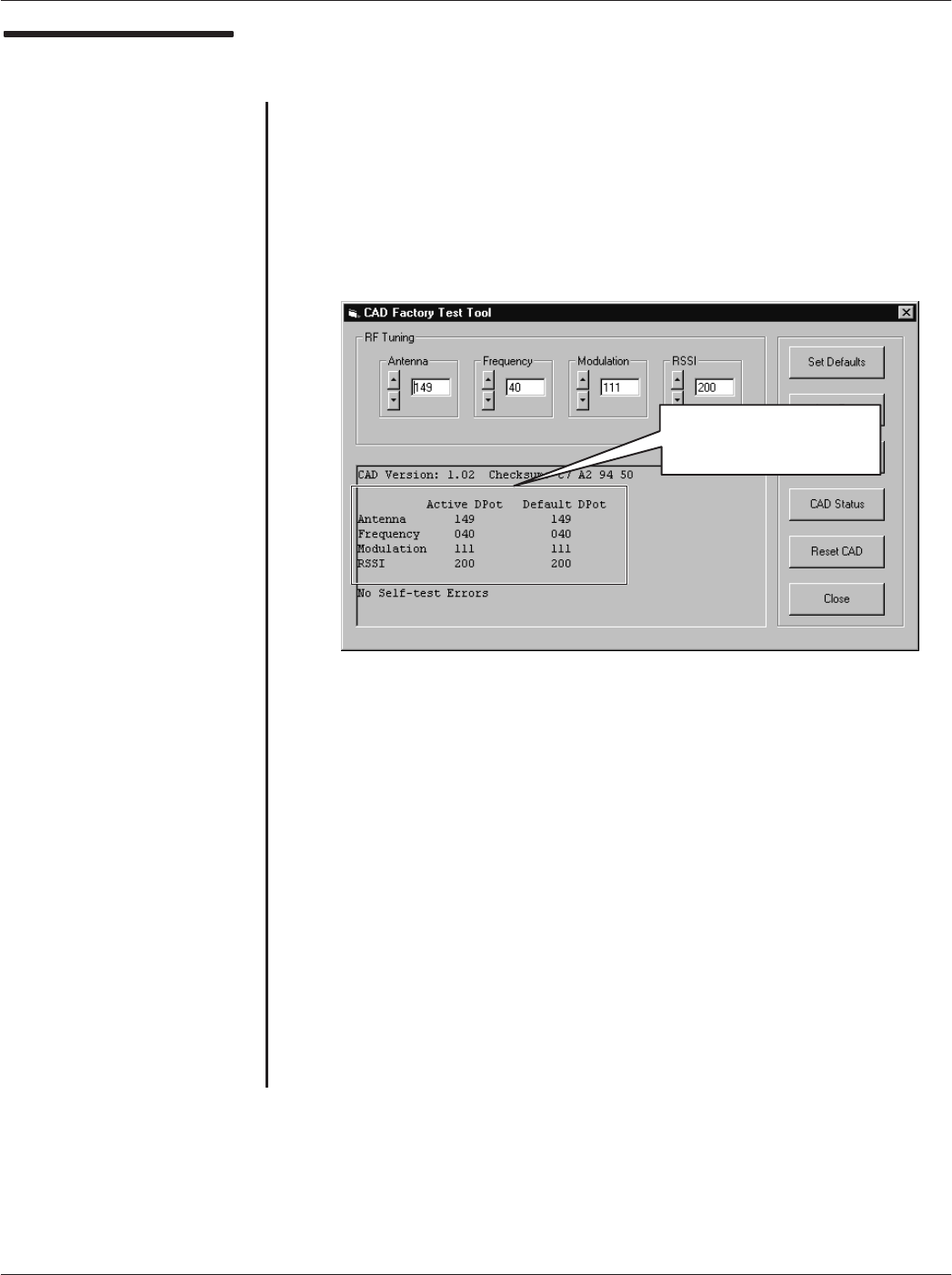
Tool main screen. Click on the CAD Status button to retrieve the
current settings from the CAD, as shown below. Jot down the
values in either the Active DPot or Default DPot column (the
values at this point should be the same).
4. Connect the Frequency Counter probe to the two wires on the
ISO Antenna. Click on the up/down arrows in the Frequency
adjustment box (to increment/decrement the value one step at at
time) and note the frequency reading on the Frequency Counter.
(Each time you click and release, the new value is sent to the
CAD and the frequency reading will change.)
5. Continue to adjust the Frequency value up or down as necessary
to obtain a reading of 13.56 MHz ±0.01%.
6. Connect the Oscilloscope probe to the two wires on the ISO
Antenna.
Ċ continued on next page Ċ
Jot Down Values in
Either of These
Two Columns
Card Acceptance Device (CAD) Technical User's Guide Motorola Confidential Proprietary
2-18 CAD001-Beta 2
5/26/99
Tuning the CAD
(continued)
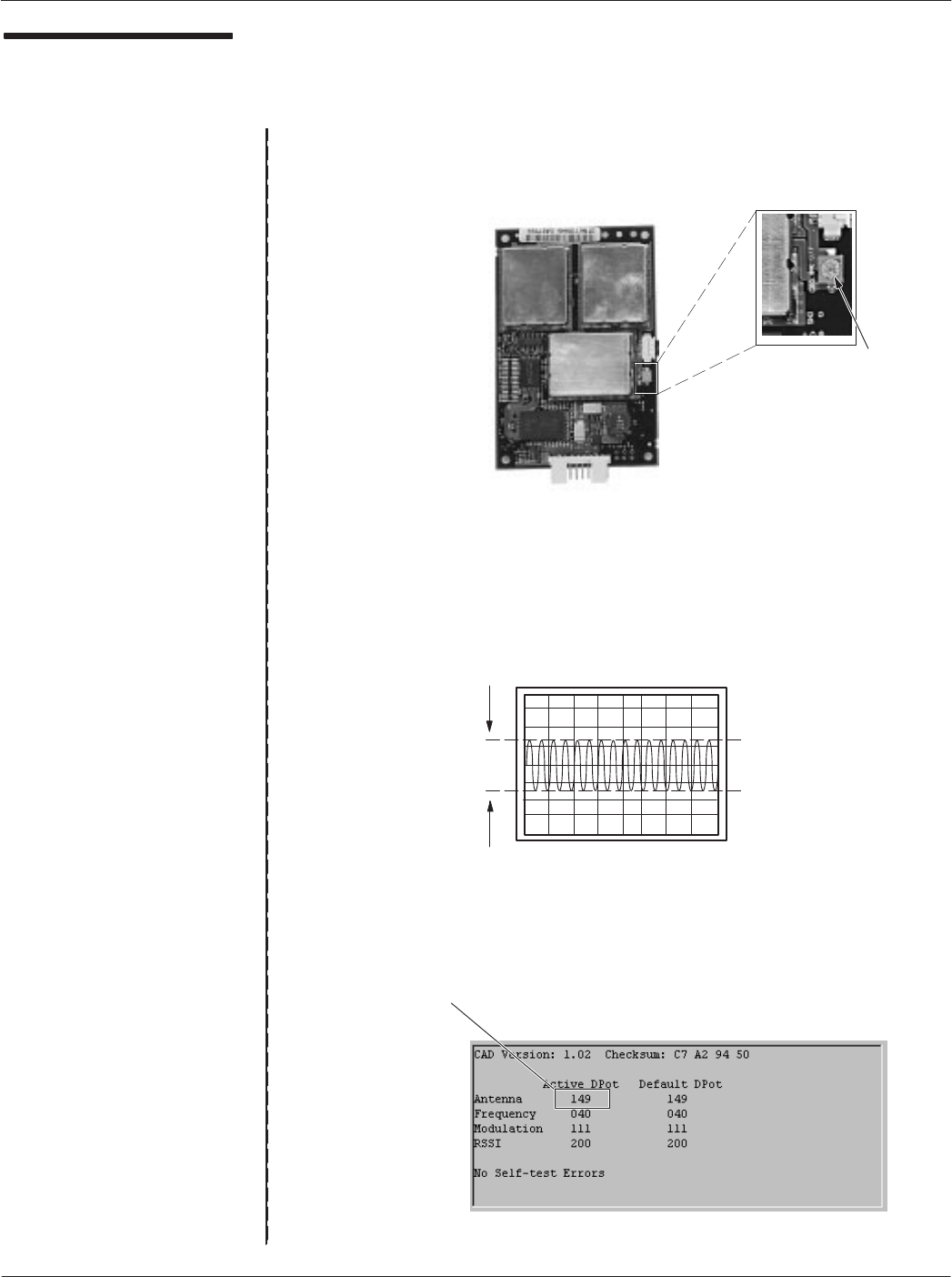
7. Locate the tuning capacitor on the CAD Control Board and
adjust it using a plastic tuning tool to achieve the maximum Vpp
reading on the oscilloscope.
8. Click on the up/down arrows in the Antenna adjustment box (to
increment/decrement the value one step at at time) and note the
waveform on the oscilloscope. Continue to adjust the Antenna
value up or down as necessary to obtain the maximum Vpp
reading (not to exceed 10.9 Vpp).
9. Click on the CAD Status button to obtain a new status report.
Note the value for the Antenna in the Active DPot column.
Maximize
Vpp Reading
Note This Value
Tuning
Capacitor

Chapter 2ąInstallationMotorola Confidential Proprietary
2-19
CAD001-Beta 2
5/26/99
Tuning the CAD
(continued)
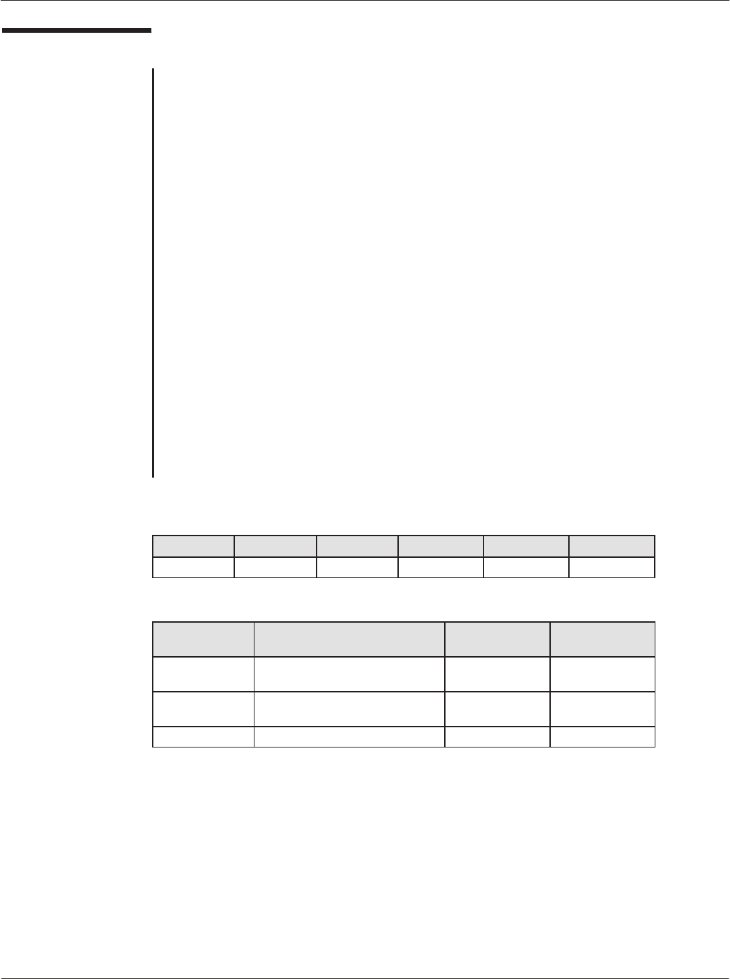
10. Look up the Antenna value in the V max column in the table
below and note the corresponding value in the Vmin (10%)
column.
11. Click on the up/down arrows in the Modulation adjustment box
(to increment/decrement the value one step at at time) to set to
the value noted in Step 3.
12. Note the Vpp waveform on the oscilloscope. Continue to adjust
the Modulation value up or down as necessary to obtain the Vpp
value noted from the table above. If this value cannot be
obtained, continue the process to obtain a value within the 8%
and 12% range (as determined by the table above).
11
10.9
10.8
10.7
10.6
10.5
10.4
10.3
10.2
10.1
10
9.9
9.8
9.7
9.6
9.5
9.4
9.3
9.2
9.1
9
8.9
8.8
8.7
8.6
8.5
8.4
8.3
8.2
8.1
8
9.370
9.285
9.200
9.115
9.030
8.944
8.859
8.774
8.689
8.604
8.519
8.433
8.348
8.263
8.178
8.093
8.007
7.922
7.837
7.752
7.667
7.581
7.496
7.411
7.326
7.241
7.156
7.070
6.985
6.900
6.815
8.820
8.740
8.659
8.579
8.499
8.419
8.339
8.259
8.178
8.098
8.018
7.938
7.858
7.777
7.697
7.617
7.537
7.457
7.377
7.296
7.216
7.136
7.056
6.976
6.895
6.815
6.735
6.655
6.575
6.495
6.414
8.298
8.223
8.147
8.072
7.996
7.921
7.846
7.770
7.695
7.619
7.544
7.468
7.393
7.318
7.242
7.167
7.091
7.016
6.940
6.865
6.789
6.714
6.639
6.563
6.488
6.412
6.337
6.261
6.186
6.111
6.035
V max V min (8%) V min (11%) V min (14%)
Card Acceptance Device (CAD) Technical User's Guide Motorola Confidential Proprietary
2-20 CAD001-Beta 2
5/26/99
Tuning the CAD
(continued)
13. Since the Modulation and Antenna adjustments are
interdependent (i.e., adjusting one affects the other), you must
now repeat Step 8 to verify that the Antenna adjustment
produces the same maximum Vpp voltage reading on the
oscilloscope as it did in Step 8. Alternate between the Antenna
adjustment and the Modulation adjustment until they both meet
the stated requirements.
14. The RSSI setting determines the threshold signal level of the
CAD's receiver circuitry. It is set to its optimal value at the factory
prior to shipment, and it is recommended that the value not be
changed. (Increasing or decreasing the RSSI value increases or
decreases the sensitivity of the receiver circuitry.)
15. Click on the Set Defaults button to store the adjustment
settings in FLASH memory on the CAD Control Board.
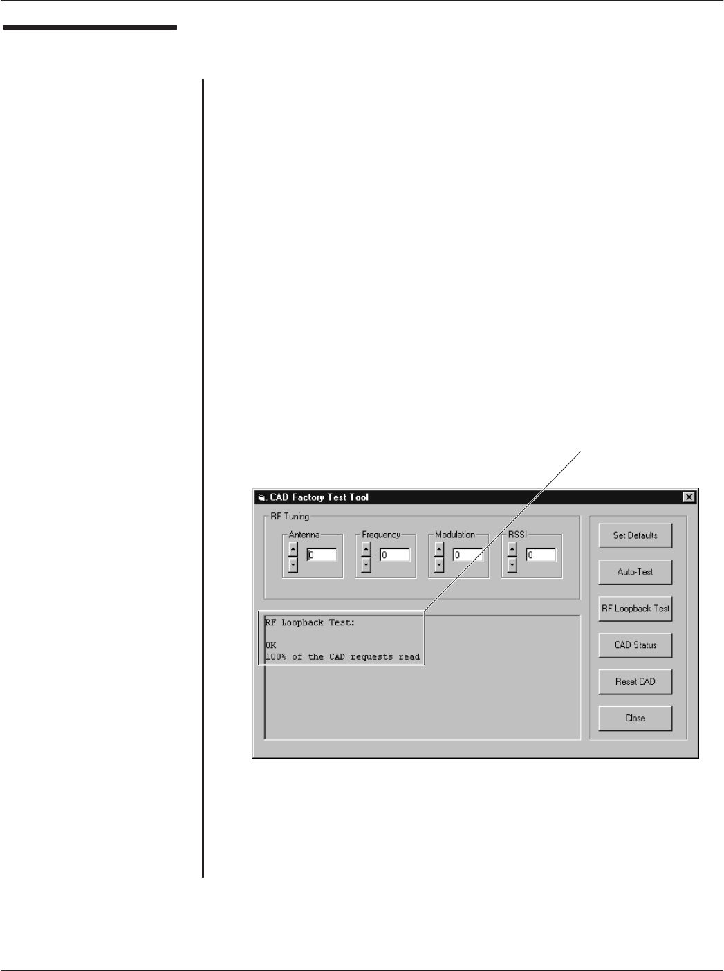
16. As a final test, place an initialized compatible SmartCard within
the reader's range (remove the ISO antenna first) and click on
the RF Loopback Test button. The following confirmation status
should appear, verifying that the CAD and SmartCard
communicated successfully.
ząEnd of this Procedureąz
RF Loopback Test
completedsuccessfully

Chapter 2ąInstallationMotorola Confidential Proprietary
2-21
CAD001-Beta 2
5/26/99
INSTALLING CAD INTO TERMINAL
4
The CAD described in this manual has been designed specifically to be installed into an AES Prodata
Model TP4000 AFC Terminal. The specific details on how to mount the CAD in the terminal and make
electrical connections are provided by AES Prodata. These details include the use of spacers and screws
to secure the CAD in the terminal and which terminal cable to connect to the CAD's RS485 connector.
The information in this section is being provided to assist in adapting the CAD to other types of
compatible enclosures, if desired.
NoteąRefer to Appendix B for pinĆout details of the CAD RS485 connector, and Appendix C for physical
dimensions and clearances.
Mounting Methods
Introduction
The CAD may be mounted in one of two ways:
DStacked (method used in the AES Prodata Model TP4000 AFC
Terminal)
DSeparated
Each of these mounting methods is described below.
Stacked" Mounting Method
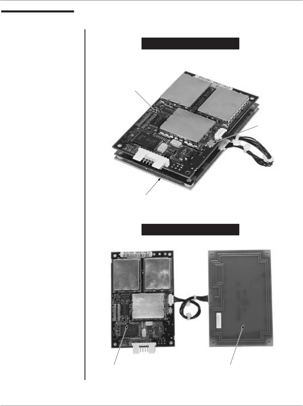
The Control Board and the Antenna Board have been designed so that
they may be stacked as shown on the facing page. The mounting holes
line up with other, and may be used with screws and spacers to secure
the CAD to the terminal chassis.
Note that the two boards may be stacked so that the metal shields on the
Control Board are either touching or not touching the metallic surface of
the Antenna Board.
Separated" Mounting Method
The 100 mm cable allow the Control Board and the Antenna Board to be
separated to accommodate various mounting scenarios, as shown on
the facing page.
Other Things You Should Know
DThe Control Board contains a tuning capacitor which must be
accessible after mounting the CAD in the terminal.
DThe nonĆmetallic side of the Antenna Board must face towards the
card reading surface of the terminal.
Card Acceptance Device (CAD) Technical User's Guide Motorola Confidential Proprietary
2-22 CAD001-Beta 2
5/26/99
Mounting Methods
ANTENNA BOARD
(METALLIC SIDE UP)
CONTROL BOARD
(CONNECTOR SIDE UP)
TUNING
CAPACITOR
CONTROL BOARD
(CONNECTOR SIDE UP)
ANTENNA BOARD
(NONĆMETALLIC SIDE FACES TOWARD
CARD READING SURFACE)
Separated" Mounting Method
Stacked" Mounting Method

Chapter 2ąInstallationMotorola Confidential Proprietary
2-23
CAD001-Beta 2
5/26/99
FINAL CHECKOUT PROCEDURE
5
Once the CAD has been tuned and installed into the terminal, a final checkout procedure must be
performed to ensure that the CAD can communicate with a compatible SmartCard. Once this final
checkout has been performed, the terminal may be placed into service.
Required Equipment
The following hardware and software is required to perform the final
checkout procedure:
DCompatible SmartCard (Model MV4000D)
DPowered terminal with CAD installed
Performing the Final
Checkout Procedure
Place an active SmartCard (one that has been initialized and
personalized for use with the particular terminal application) within
reading distance (typically 10 cm) and verify that the desired results are
achieved. For example, for a transit application, the terminal should
generate a receipt ticket.

Card Acceptance Device (CAD) Technical User's Guide Motorola Confidential Proprietary
2-24 CAD001-Beta 2
5/26/99
THIS PAGE INTENTIONALLY LEFT BLANK

Chapter 3 "Troubleshooting
Card Acceptance Device (CAD)
Technical User's Guide
CAD001-Beta 2
5/26/99
chapter contents
Fault Isolation Procedures 2
Returning Faulty CADs to Motorola 3

Card Acceptance Device (CAD) Technical User's Guide
3-2 CAD001-Beta 2
5/26/99
1FAULT ISOLATION PROCEDURES
There are four basic techniques for isolating the CAD as the source of a faulty terminal:
DVerify dc power from the terminal (+12 V dc)
DObserve LED Indicator on the Control Board
DPerform the Self Test diagnostics checkout procedure
DPerform the Tuning Procedure
Verify DC Power
With the terminal turned on, the CAD should be receiving +12 V
dc on pin 3 of the RS485 connector located on the Control Board
(use pin 2 as ground). Verify that the voltage is present using a
digital voltmeter. If the dc voltage is not present:
DMake sure the cable from the terminal is securely attached
to the 10Ćpin connector on the Control Board.
DTroubleshoot the terminal to determine source of faulty
+12 V dc.
Verify LED Indicator
A green LED is provided on the Control Board to provide a visual
indication that the Control board has received dc power and has
successfully performed its startup routine. If this LED is not lit
after applying power:
DVerify +12 V dc power from the terminal (see above)
DReload the CAD operating software into FLASH memory
(refer to Appendix A in this manual)
Perform the Self Test
Checkout Procedure
Run the Self Test Utility as described in Chapter 2.
Perform the CAD Tuning
Procedure
Perform the CAD tuning procedure as described in Chapter 2.

Chapter 3ąTroubleshooting
3-3
CAD001-Beta 2
5/26/99
2RETURNING FAULTY CADS TO MOTOROLA
If you have performed the troubleshooting procedures on page 2 and have determined that the CAD is
faulty, return the entire CAD (Control Board, Antenna Board, and interconnect cable) to the address
listed below. The faulty CAD will be either repaired or replaced by Motorola service personnel.
Return Faulty CADs to:
WHERE DO WE HAVE DEFECTIVE CADS SENT ????xxx

Card Acceptance Device (CAD) Technical User's Guide
3-4 CAD001-Beta 2
5/26/99
Notes...

Chapter 4 "Functional Theory of Operation
Card Acceptance Device (CAD)
Technical User's Guide
CAD001-Beta 2
5/26/99
chapter contents
Functional Theory of Operation 2

Card Acceptance Device (CAD) Technical User's Guide
4-2 CAD001-Beta 2
5/26/99
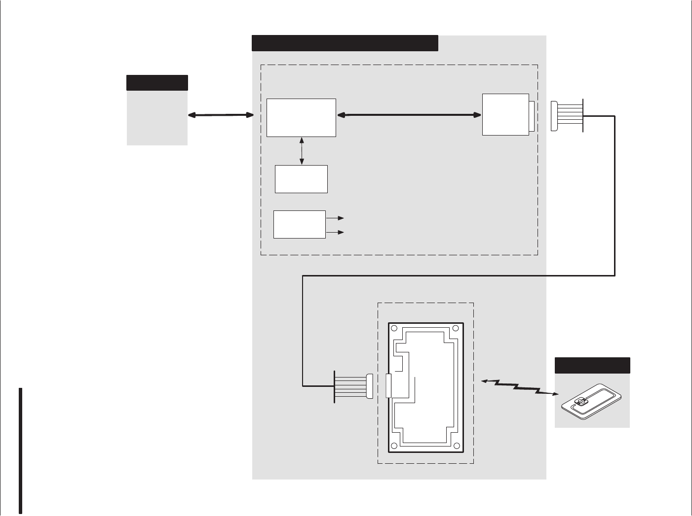
FUNCTIONAL THEORY OF OPERATION
1
The following theory of operation describes the operation of the CAD circuitry at a functional level. The information
is presented to give the service technician a basic understanding of the functions performed by the CAD in order
to facilitate fault isolation. Refer to NO TAG for a block diagram of the CAD.
Microprocessor Circuitry
Overview
The CAD uses a Motorola ColdFire MCF5204 microprocessor (mP)
which serves as the main controller for the CAD. The microprocessor,
running at a clock speed of 18.432 MHz (generated by an external
clock circuit) controls the operation of the CAD as determined by the
CAD software contained in the FLASH memory.
Address and Data Buses
The mP is equipped with a 21Ćline address bus used to access the
memory (FLASH and SRAM) and provide control (via memory mapĆ
ping) for other circuitry in the CAD. A 16Ćline data bus is used to transfer
data to/from the mP, memory, and the AFE.
Terminal Interface
Data from the mP to the terminal (TXD) is sent via an internal UART port
on the mP through an RS485 converter to the 10Ćpin connector P4.
Data from the terminal to the mP (RXD) is sent via the 10Ćpin connector
P4. through a RS485 converter to an internal UART port on the mP.
Reset Circuit
A Low +5V Detect circuit monitors the level of the +5V supply voltage
and generates a reset signal if it falls below a threshold level. The reset
signal is sent to the mP, the I/O Register, the AFE, and FLASH memory.
NonĆVolatile Memory Circuitry
FLASH Memory
The CAD software resides in a 256k x 16 FLASH memory IC. The
FLASH memory is accessed by the mP via the 21Ćline Address Bus and
the 16Ćline Data Bus.
SRAM Memory
To supplement the mP's internal 512 bytes of internal SRAM, a 32k x 8
SRAM IC is provided.

Chapter 4ąFunctional Theory of Operation
4-3
CAD001-Beta 2
5/26/99
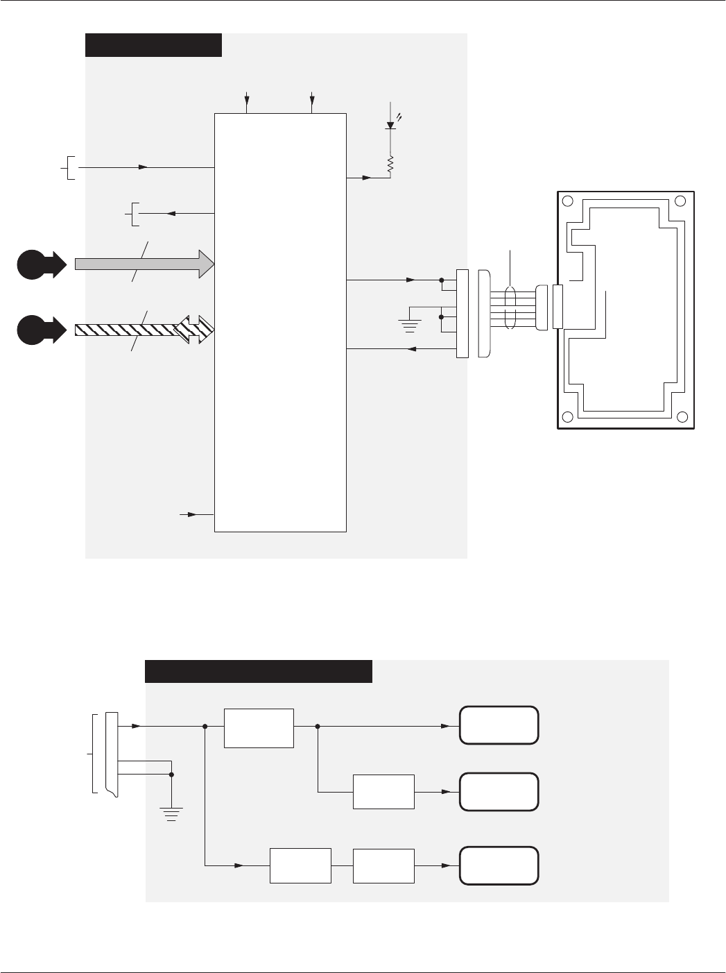
AFE Circuitry
The Analog Front End (AFE) circuitry operates under control of the mP
to provide a number of functions, as follows:
DControls the power output to the antenna
DModulates TX data and sends to card (via Antenna Board)
DReceives (via Antenna Board) RX data from card and provides
demodulation
Supply Voltages Circuitry
The CAD Control Board contains onĆboard regulators and filtering cirĆ
cuitry to generate the various voltages required by the CAD circuitry.
+12 V from the terminal (via connector P4) is used as the source to
generate +5V and +5V_A supply voltages. Also, the variable PA_PWR
supply voltage is generated and fed to the Power Amplifier (p/o AFE)
to control the RF output power of the CAD.
Antenna Board
The Antenna Board consists of a printed circuit board (with traces that
form the antenna), a ferrite plate (which magnetically shields the antenĆ
na from the Control Board), and a metal back plate (which electrically
shields the antenna from the Control Board). The Antenna Board is
connected to the Control Board by a 6Ćwire cable.
Card Acceptance Device (CAD) Technical User's Guide
4-4 CAD001-Beta 2
5/26/99
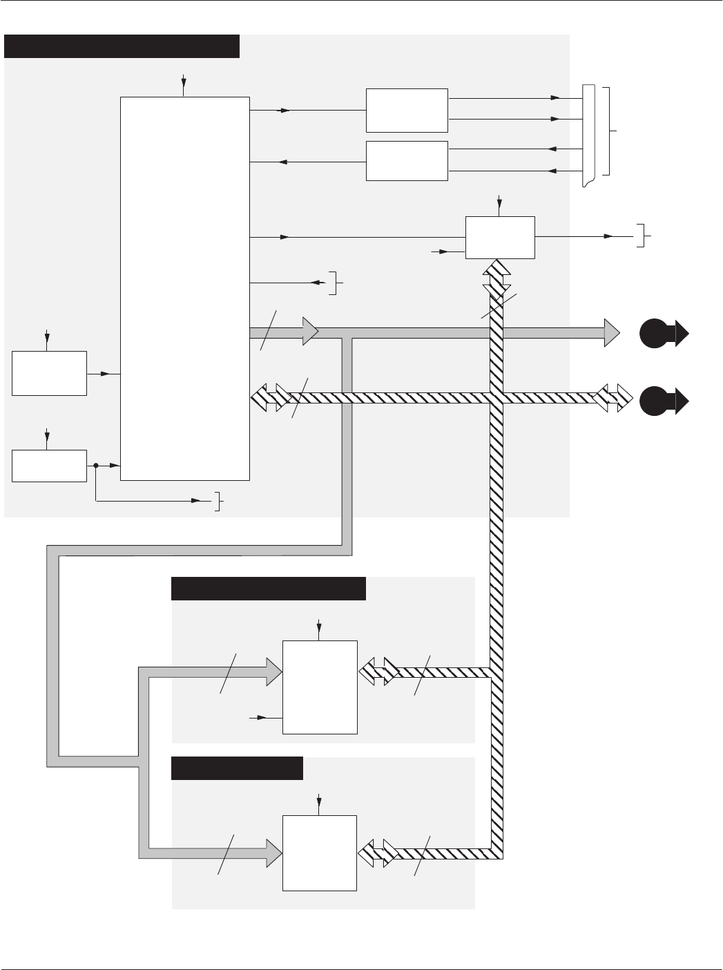
SRAM MEMORY
MICROPROCESSOR
A1-A20
FLASH
256K X 16
SRAM
32KX8
DATA BUS
ADDRESS BUS
NON-VOLATILE MEMORY
MICROPROCESSOR CIRCUITRY
ADDRESS BUS
ADDRESS
DATA
Figure 1. Card Access Device (CAD) Functional Block Diagram (1 of 2)
18.432 MHz
OSCILLATOR
CIRCUITRY CLK
+5V
A0-A14
+5V
D0-D15
D0-D15
A0-A20
TXD
RXD
D8-D15
P/O P4
RS485
CONVERTER
TXA
TXB
RS485
CONVERTER
RXA
RXB
I/O
REGISTER
CS05
7
6
5
4
MATES WITH
CABLE FROM
TERMINAL
+5V
AFE_CONTROLS
LOW +5V
DETECT RESET
+5V
TO OTHER
DEVICES
RESET
+5V
D8-D13
AFE_CONTROL FROM
AFE
RESET
RESET
+5V
A
B
TO
AFE
Chapter 4ąFunctional Theory of Operation
4-5
CAD001-Beta 2
5/26/99
ANTENNA
BOARD
P6
5
6ĆWIRE
CABLE
6
3
4
2
1
ANALOG
FRONT END
(AFE)
D8-D15
A0-A3
+5V_A
AFE_CONTROL
+5V
AFE
STATUS
INDICATOR
AFE CIRCUITRY
SUPPLY VOLTAGES CIRCUITRY
+5V
FILTER
CIRCUITRY
+5V
REGULATOR
3
MATES WITH
CABLE FROM
TERMINAL
P/O P4
+5V_A
2
9
TO
mP
RESET
ADJUSTABLE
REGULATOR PA_PWR
PA_PWR
FILTER
CIRCUITRY
A
B
AFE_CONTROLS
FROM
mP
ANTENNA_COIL
RECEIVE SIGNAL
Figure 1.ąCard Access Device (CAD) Functional Block Diagram (2 of 2)

Card Acceptance Device (CAD) Technical User's Guide
4-6 CAD001-Beta 2
5/26/99
THIS PAGE INTENTIONALLY LEFT BLANK

Chapter 5 "CAD Protocols and Commands
Card Acceptance Device (CAD)
Technical User's Guide
CAD001-Beta 2
5/26/99
chapter contents
TerminalĆtoĆCAD Command Protocol 2
Answer to Reset (ATR) 6
CAD Management Commands 8
Command Sequences 28
Card Acceptance Device (CAD) Technical User's Guide
5-2 CAD001-Beta 2
5/26/99
1TERMINALĆTOĆCAD COMMAND PROTOCOL
This section defines the structure of commands initiated by the terminal for transmission control and
for specific control in asynchronous halfĆduplex transmission protocols. Block protocol type T=1 is
used.
The command structure (shown below) consists of the following blocks:
Dprologue field
Dinformation field
Depilogue field
The prologue and epilogue fields are mandatory, and must be sent in every case. The information field
is optional. The number of bytes of the information field is indicated by length (LEN) byte (part of the
prologue field).
Command Structure
Prologue Field Information Field Epilogue Field
NAD PCB LEN Inf EDC
1 Byte 1 Byte 1 Byte 0 to 254 Bytes 1 or 2 Bytes
Prologue Field
NAD
The NAD byte in the Prologue field contains the block's target
(DAD) and source (SAD) node addresses, as shown below.
NAD Byte Structure
b1 b2 b3 b4 b5 b6 b7 b8 Meaning
x xx x ---- DAD (Destination Node Address)
----xxxx SAD (Source Node Address)
Chapter 5ąCAD Protocols and Commands
5-3
CAD001-Beta 2
5/26/99
Prologue Field
(continued)
PCB
The PCB byte in the Prologue field serves to control and
supervise the transmission protocol. The PCB byte encodes first
and foremost the block type, as well as supplementary data
needed in this context. The PCB byte information for an IĆblock,
an RĆblock, and an SĆblock are shown below.
PCB Byte Information for an IĆBlock
b1 b2 b3 b4 b5 b6 b7 b8 Meaning
0 ------- Signals IĆblock
0 N(S) - 0 0 0 0 0 Send sequence number
0-x00000 Chaining (more data)
PCB Byte Information for an RĆBlock
b1 b2 b3 b4 b5 b6 b7 b8 Meaning
1 00 ----- Signals RĆblock
1 0 0 N(R) - - - - Sequence Number
1 0 0 N(R) 0 0 0 0 No errors
1 0 0 N(R) 0 0 0 1 EDC or parity error
1 0 0 N(R) 0 0 1 0 Other errors
PCB Byte Information for an SĆBlock
b1 b2 b3 b4 b5 b6 b7 b8 Meaning
11------- Signals SĆblock
1 1000000 RESYNCH req = C0
1 1100000 RESYNCH ans = E0
1 1000010 Abort request = C2
1 1100010 Abort response = E2
1 1000011 WTX request = C3
1 1100011 WTX response = E3
11xxxxxx RFU values used for the CAD manageĆ
ment

Card Acceptance Device (CAD) Technical User's Guide
5-4 CAD001-Beta 2
5/26/99
Information Field (INF)
The presence of INF is optional. When present, INF conveys
either application data in IĆblocks for cards, miscellaneous data
for the CAD or nonĆapplication control and status information in
SĆblocks.
In an SĆblock, this field is used for the management of the CAD.
The CAD does not support the exhaustive list of SĆBlocks defined
in ISO 7816-3 T=1. However, the CAD supports Motorola
proprietary definition of SĆBlocks as commands for
management.
RĆblocks do not contain an INF field.
Epilogue Field
This field contains the error detection code (EDC) of the
transmitted block. The protocol definition permits this to be either
an LRC or a CRC. The LRC is calculated as the exclusive OR
(XOR) of all the bytes starting with the NAD through the last byte
of the information field, and is typically referred to simply as the
checksum. For CRC see ISO 3309. The CAD uses the CRC.

Chapter 5ąCAD Protocols and Commands
5-5
CAD001-Beta 2
5/26/99
THIS PAGE INTENTIONALLY LEFT BLANK
Card Acceptance Device (CAD) Technical User's Guide
5-6 CAD001-Beta 2
5/26/99
2ANSWER TO RESET (ATR)
After cycling the power supply or software reboot, the CAD sends out an ATR at 9.6 KBPS on the
serial link. Then the CAD switches to 115,2 KBPS for all other communications.
The ATR is a data string, up to 33 bytes long, which contains various data relevant to the transmission
protocol and to the card. The ATR's data string and data elements are defined and described in detail
in ISO/IEC 7816-3. The structure of the ATR is the initial character TS followed by a variable number
of subsequent characters in the following order: the format character T0, optionally the interface
characters TAi, TBi, TCi, TDi and optionally the historical characters T1 T2 - TK and, conditionally, the
check character TCK.
ATR Format
The basic ATR format consists of:
DTS Ċ one byte, the initial character; specifies the conĆ
ventions to code data bytes in all subsequent characĆ
ters. There are two possible values of TS (ten consecĆ
utive bits from start to end and corresponding hexadeĆ
cimal value). The CAD uses direct convention:
(Z)AZZAZZZAAZ(Z) where logic level ONE is Z (LSB
is first). It equals to "3B" when decoded by direct conĆ
vention.
DT0 Ċ one byte, the format character; serves to indiĆ
cate the subsequent "interface character" a bit field is
used, from b5 to b8. It further contains the number of
subsequent "historical characters," from b1 to b4.
T0 Byte Information
b1 b2 b3 b4 b5 b6 b7 b8 Meaning
--- 1 ---- TA1 is transmitted
--1 ----- TB1 is transmitted
- 1------ TC1 is transmitted
1 ------- TD1 is transmitted
----xxxx Number of historical characters
Chapter 5ąCAD Protocols and Commands
5-7
CAD001-Beta 2
5/26/99
ATR Format (continued)
The four least significant bits of any interface byte TDi indicates
a protocol type T, specifying rules to be used to process
transmission protocols. When TD1 is not transmitted, T=0 is
used. TA1 TB1 TC1 and TB2 are the global interface bytes. These
global interface bytes shall be interpreted in order to process any
transmission protocol correctly.
The interface characters specify all transmission parameters of
the current protocol. They are constructed from the bytes TAI,
TBI, TCI, and TDi (i =1, 2, 3-). TA, TBi and TCi indicate the
protocol parameters. Their interpretation depends on the
protocol type indicated by T in TDi-1. TDi indicates the protocol
type T, as defined in [1] Section 6.1.4.3, and the presence of
subsequent interface characters. The ATR transmission of these
bytes is optional and may be omitted if appropriate.
TDi Byte Information
b1 b2 b3 b4 b5 b6 b7 b8 Meaning
--- 1 ---- TAi+1 is transmitted
--1 ----- TBi+1 is transmitted
- 1------ TCi+1 is transmitted
1 ------- TDi+1 is transmitted
----xxxx Protocol type for subsequent transmisĆ
sion
When TDi is not transmitted, the default value of TAi+1 TBi+1
TCi+1 is null, indicating that no further interface characters
TAi+1 TBi+1 TCi+1 TDi+1 will be transmitted. TA1 to TC3
convey information that shall be used during exchanges
between the terminal and the CAD subsequent to the Answer to
Reset. They indicate the values of the transmission control
parameters F, D, I, P, and N, and the IFSC, block waiting time
integer (BWI), and character waiting time integer (CWI)
applicable to T=1 as defined in ISO/IEC 7816-3. The
information contained in TA1 to TC1 and TC2 shall apply to all
subsequent exchanges.
The historical characters, T1 T2 -TK, maximum 15 characters.
It designates general information, for example, the CAD firmware
version.
The value of check character TCK shall be such that the
exclusive-ORing of all bytes from byte T0 to the last byte before
the TCK.

Card Acceptance Device (CAD) Technical User's Guide
5-8 CAD001-Beta 2
5/26/99
3CAD MANAGEMENT COMMANDS
Commands in proprietary SĆBlocks supported by the CAD are:
DRF POWER CONTROL: control of the RF field parameters
DSLEEP: put the CAD in low power mode
DDOWNLOADING: put the CAD in downloading mode
DERROR REPORT: the CAD indicates an Hardware error
DPOLL: put the CAD in card registration mode
DANSWER TO POLL: the CAD sends the parameters of a card detected
DDETECT CARD: put the CAD in card detection mode
DCARD PRESENCE: the CAD sends to the terminal the result of the DETECT CARD comĆ
mand.
DREBOOT: forces the CAD to reset
Note that not all of these commands follow the request/response pair scheme.

Chapter 5ąCAD Protocols and Commands
5-9
CAD001-Beta 2
5/26/99
THIS PAGE INTENTIONALLY LEFT BLANK
Card Acceptance Device (CAD) Technical User's Guide
5-10 CAD001-Beta 2
5/26/99
RF POWER
CONTROL
RF POWER CONTROL request
Description
This command allows the terminal to control the RF field power. The four options
of the PCON byte can turn on the 13.57MHz carrier, turn off the carrier, increase
the power of the RF field and to decrease the power of the RF field.
Direction
Terminal to CAD
Size
6 Bytes
Format
See below
RF POWER CONTROL Request Format
NAD PCB LEN PCON CRC1 CRC2
0x11 0xC5 1 (see below) (see below) (see below)
PCON Values Meaning CRC1 Values CRC2 Values
0x00 Power On 0x3B 0x09
0x01 Power Off 0xB2 0x18
0x02 Decrease Power 0x29 0x2A
0x03 Increase Power 0xA0 0x3B
Other Values Forbidden Ċ Ċ

Chapter 5ąCAD Protocols and Commands
5-11
CAD001-Beta 2
5/26/99
RF POWER
CONTROL
(continued)
RF POWER CONTROL response
Description
The response frame is an acknowledgement of the previous command,
indicating that the command was properly received and has been executed.
Direction
CAD to Terminal
Size
5 Bytes
Format
See below
RF POWER CONTROL Response Format
NAD PCB LEN CRC1 CRC2
0x11 0xE5 0 0xA4 0x8E
Card Acceptance Device (CAD) Technical User's Guide
5-12 CAD001-Beta 2
5/26/99
SLEEP
SLEEP request
Description
This command switches the CAD board to a lowĆpower mode. It sequentially
turns off the RF power, stops watchdog timer, unmask only the UART interrupt
and switches to the STOP mode of the ColdFire. While no interrupt from the
UART is received (any frame from the terminal), the CAD stays in this mode. Any
UART interrupt wakes the CAD processor core, turns on the RF power and
switches to the state of frame reception.
Direction
Terminal to CAD
Size
5 Bytes
Format
See below
SLEEP Request Format
NAD PCB LEN CRC1 CRC2
0x11 0xC8 0 0xEF 0x1D
SLEEP response
Description
The response frame is an acknowledgment of the previous command that
indicates that the command was properly received and is ready to be executed.
This response is sent before the CAD switches to SLEEP state.
Direction
CAD to Terminal
Size
5 Bytes
Format
See below
SLEEP Response Format
NAD PCB LEN CRC1 CRC2
0x11 0xE8 0 0xDC 0x3E

Chapter 5ąCAD Protocols and Commands
5-13
CAD001-Beta 2
5/26/99
THIS PAGE INTENTIONALLY LEFT BLANK
Card Acceptance Device (CAD) Technical User's Guide
5-14 CAD001-Beta 2
5/26/99
DOWNLOADING
DOWNLOADING request
Description
This command makes the CAD switch to downloading mode. The code of the
Parameters 1 & 2, processor and FPGA can be downloaded by selecting the
TARGET byte 0x00.
This command must be sent both at the beginning and at the end of the
downloading sequence. At the end of the downloading sequence, this
command confirms that the downloading sequence is correctly complete and
provokes the reset of the CAD processor. The TARGET field of this last block
must be identical to the TARGET field of the previous DOWNLOADING
command.
Direction
Terminal to CAD
Size
6 Bytes
Format
See below
DOWNLOADING Request Format
NAD PCB LEN TARGET CRC1 CRC2
0x11 0xC6 1 (see below) (see below) (see below)
TARGET
Values Meaning CRC1 Values CRC2 Values
0x00 Parameters 1Ć2, MCU, and
FPGA Code
0x5F 0x6E
0x01 All FLASH Code (including Boot
Block)
0xD6 0xF7
Other Values RFU RFU RFU
Chapter 5ąCAD Protocols and Commands
5-15
CAD001-Beta 2
5/26/99
DOWNLOADING
(continued)
DOWNLOADING response
Description
The response frame is an acknowledgment of the previous command that
indicates that the command was properly received and is ready to be executed.
Direction
CAD to Terminal
Size
5 Bytes
Format
See below
DOWNLOADING Response Format
NAD PCB LEN CRC1 CRC2
0x11 0xE6 0 0xCC 0xA4
Card Acceptance Device (CAD) Technical User's Guide
5-16 CAD001-Beta 2
5/26/99
ERROR REPORT
ERROR REPORT request
Description
The CAD sends this command to the terminal if the CAD software has detected
an error during the test sequence at boot up. The tests executed by the CAD at
boot-up are the verification of the processor code checksum, the verification
of the FPGA code and an UART test in loopback mode. If the CAD detects any
of these errors, it immediately sends this frame to the terminal after the ATR
frame.
Direction
CAD to Terminal
Size
6 Bytes
Format
See below
ERROR REPORT Request Format
NAD PCB LEN ERR CRC1 CRC2
0x11 0xC7 1 (see below) (see below) (see below)
ERR Values Meaning CRC1 Values CRC2 Values
0x00 No Error 0x83 0xBC
0x01 Code Checksum Error 0x0A 0xAD
0x02 FPGA Code Error 0x91 0x9F
0x03 UART Initialization Error 0xA7 0xFA
0x04 SRAM Error 0xCB 0x30
Other Values RFU RFU RFU
ERROR REPORT response
There is no response for the ERROR REPORT command.

Chapter 5ąCAD Protocols and Commands
5-17
CAD001-Beta 2
5/26/99
THIS PAGE INTENTIONALLY LEFT BLANK
Card Acceptance Device (CAD) Technical User's Guide
5-18 CAD001-Beta 2
5/26/99
POLL
POLL request
Description
This command makes the CAD switch to the card detection/anti-collision
sequence.
The STRAT byte supports two options that order the CAD to detect all cards (Long
Poll) or the first card (Quick Poll) in the RF field.
As the CAD manages the attribution of the NAD for the cards detected in the field,
it reserves NAD values that are already in use and gives free NAD values to a new
card that is detected. But the CAD has no information about the transactions
between the terminal and the card(s). Thus, when the terminal has completed all
the transactions with the card(s) registered, it may indicate to the CAD that the busy
values can be freed or not by setting the appropriate value in the ERASE field.
The TYPE byte of this command indicates to the CAD which type of application
of contactless card in the field must be selected.
Direction
Terminal to CAD
Size
8 Bytes
Format
See below
POLL Request Format
NAD PCB LEN STRAT ERASE TYPE CRC1 CRC2
0x11 0xD0 3 (see
below)
(see
below)
(see
below)
xx xx
STRAT
Values Meaning ERASE
Values Meaning
0x00 Quick Poll 0x00 Do not erase NAD table
0x01 Long Poll 0x01 Erase NAD table
Other Values RFU Other Values Forbidden
TYPE
Values Meaning TYPE
Values Meaning
0x00 All 0x06 Multimedia
0x01 Transport 0x07 Gaming
0x02 Financial 0x08 Data Storage
0x03 Identification 0x09-0x7E RFU
0x04 Telecommunication 0x7F All previous
0x05 Medical 0x80-0xFF Proprietary
Chapter 5ąCAD Protocols and Commands
5-19
CAD001-Beta 2
5/26/99
POLL (continued)
POLL response
Description
The response frame is an acknowledgment of the previous command that
indicates that the command was properly received and is ready to be executed.
Direction
CAD to Terminal
Size
5 Bytes
Format
See below
POLL Response Format
NAD PCB LEN CRC1 CRC2
0x11 0xF0 0 0x8D 0x65
Card Acceptance Device (CAD) Technical User's Guide
5-20 CAD001-Beta 2
5/26/99
ANSWER TO
POLL
ANSWER TO POLL request
Description
When a card is successfully registered in the CAD (the card answered correctly to the
REQUEST SLOT MARKER and ATTRIB frames), the CAD sends this frame to the
terminal to indicate that a new card is to be registered. The ATPoll request frame
transports all necessary information about the card and the card-terminal link.
The NEW NAD byte is the value of the NAD that will be used by the terminal and the
card during the transaction. This NAD is ISO 7816-3 T=1 compliant. The terminal
must use the value received in the ATPoll command to sent data to the card, without
inverting the most significant and the least significant nibble of the byte.
The four-byte PUPI field identifies formally the card. The terminal may use it to
detect non-valid cards.
The HB field may be n bytes long (0-15) and is the exact image of the Historical
Bytes field of the card ATQ frame.
Direction
CAD to Terminal
Size
12+n Bytes
Format
See below
ANSWER TO POLL Request Format
NAD PCB LEN DATA from the ATQ CRC1 CRC2
0x11 0xD1 7 +n* NEW NAD PUPI TC2 TA3 HB xx xx
* n = number of Historical Bytes (HB)
DATA from ATQ
Values Meaning
NEW NAD NAD chosen by the CAD for the new TerminalĆCard link
PUPI 4Ćbyte Card Identifier (Pseudo Unique PICC Identifier)
TC2 POW (Minimum and Maximum Power Level
TA3 LEN (Maximum Block Length)
HB Historical Bytes from the ATQ frame
ANSWER TO POLL response
There is no response for the ANSWER TO POLL command.

Chapter 5ąCAD Protocols and Commands
5-21
CAD001-Beta 2
5/26/99
THIS PAGE INTENTIONALLY LEFT BLANK
Card Acceptance Device (CAD) Technical User's Guide
5-22 CAD001-Beta 2
5/26/99
DETECT CARD
DETECT CARD request
Description
After a Quick Poll command, the DETECT CARD command may be sent by the
terminal to know if there are additional cards in non-application phase into the RF
field. After this command, the CAD sends a REQUEST command parametrized
with 1 slot through the RF field. Consequently, if one or more additional cards
are present in the RF field, it must answer to the REQUEST command. The card
which is communicating with the Terminal will not answer to the REQUEST if it
has not received a DESELECT command (see ISO/IEC 14443-3).
The TYPE byte of this command indicates to the CAD which type of application
of contactless card in the field must be detected.
Whatever is the result of the detection (nothing, a collision or a correct answer),
the CAD uses the CARD PRESENCE command to indicate the result of this
detection sequence.
NoteąSince this command is to be sent after a Quick Poll command, do not try to
send this command under any other circumstances (like immediately after reboot).
Direction
Terminal to CAD
Size
6 Bytes
Format
See below
DETECT CARD Request Format
NAD PCB LEN TYPE CRC1 CRC2
0x11 0xC7 1 (see below) (see below) (see below)
TYPE Values Meaning CRC1 Values CRC2 Values
0x00 All 0x77 0x5A
0x01 Transport 0xFE 0x4B
0x02 Financial 0x65 0x79
0x03 Identification 0xEC 0x68
0x04 Telecommunication 0x53 0x1C
0x05 Medical 0xDA 0x0D
0x06 Multimedia 0x41 0x3F
0x07 Gaming 0xC8 0x2E
0x08 Data Storage 0x3F 0xD6
0x09-0x7E RFU RFU RFU
0x7F All Previous 0x07 0xD1
0x80-0xFF Proprietary Proprietary Proprietary

Chapter 5ąCAD Protocols and Commands
5-23
CAD001-Beta 2
5/26/99
DETECT CARD
(continued)
DETECT CARD response
There is no response for the DETECT CARD command.
Card Acceptance Device (CAD) Technical User's Guide
5-24 CAD001-Beta 2
5/26/99
CARD PRESENCE
CARD PRESENCE request
Description
The CAD sends this frame to the terminal as a result of the card detection
sequence initiated by the DETECT CARD command.
The PRES byte of the command indicates if something new is detected or not.
Direction
CAD to Terminal
Size
6 Bytes
Format
See below
CARD PRESENCE Request Format
NAD PCB LEN PRES CRC1 CRC2
0x11 0xD4 1 (see below) (see below) (see below)
PRES Values Meaning CRC1 Values CRC2 Values
0x00 No Card 0x72 0xD6
0x01 Additional Card(s) Detected 0xFB 0xC7
Other Values Forbidden Ċ Ċ
CARD PRESENCE response
There is no response for the CARD PRESENCE command.
Chapter 5ąCAD Protocols and Commands
5-25
CAD001-Beta 2
5/26/99
REBOOT
REBOOT request
Description
This command makes the CAD processor reset. After this command is executed
the CAD board is reset and any configuration different from the CAD default
configuration is lost.
Direction
Terminal to CAD
Size
5 Bytes
Format
See below
REBOOT Request Format
NAD PCB LEN CRC1 CRC2
0x11 0xD2 0 0x0E 0x75
REBOOT response
Description
The response frame is an acknowledgment of the previous command that
indicates that the command was properly received and is ready to be executed.
Direction
CAD to Terminal
Size
5 Bytes
Format
See below
REBOOT Response Format
NAD PCB LEN CRC1 CRC2
0x11 0xF2 0 0x3D 0x56

Card Acceptance Device (CAD) Technical User's Guide
5-26 CAD001-Beta 2
5/26/99
BREAK
CHARACTER
BREAK CHARACTER request
Description
A break character makes the CAD processor reset. After this character is sent,
the CAD board is reset and any configuration different from the CAD default
configuration is lost.
Direction
Terminal to CAD
Size
1 Bytes
Format
All the bits are set to 0. The Stop Bit is included.
BREAK CHARACTER response
Description
There is no response to the BREAK CHARACTER command.

Chapter 5ąCAD Protocols and Commands
5-27
CAD001-Beta 2
5/26/99
THIS PAGE INTENTIONALLY LEFT BLANK

Card Acceptance Device (CAD) Technical User's Guide
5-28 CAD001-Beta 2
5/26/99
4COMMAND SEQUENCES
The illustrations on the next few pages show the command sequences between the Terminal, CAD,
and Card for the following scenarios:
DBoot Sequence
DDownloading Sequence
DQuick Poll Sequence
DLong Poll Sequence
DDetect Card Sequence
DRF Power Control Sequence
DSleep Sequence
DReboot Sequence
Chapter 5ąCAD Protocols and Commands
5-29
CAD001-Beta 2
5/26/99
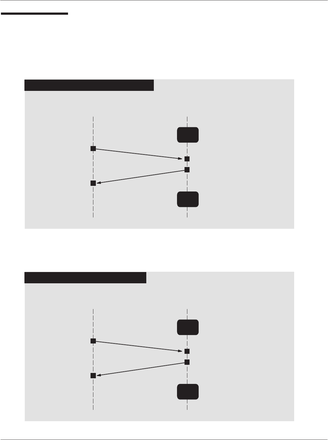
Boot Sequence
TERMINAL CAD
ATR
DąCPU registers configuration
DąRun AutoĆTests
DąFPGA Code Loading
DąConfigure UART at 9600 BPS
DąConfigure UART at 115200 BPS
DąWait for first command from terminal
NORMAL BOOT SEQUENCE
BOOT SEQUENCE WITH HARDWARE ERROR
TERMINAL CAD
ATR
DąCPU registers configuration
DąAutoĆTest Fails
DąConfigure UART at 115200 BPS
Decode
CAD
Parameters Continue
Power Up
Power
Up
Power
Up
Finish
Power
Up
Decode
CAD
Parameters
Error Report
DąSwitch to download process
DąWait for the first I-Block of downloading
Finish
Power
Up
Prepare
Data to
Download
Card Acceptance Device (CAD) Technical User's Guide
5-30 CAD001-Beta 2
5/26/99
Downloading
Sequence
TERMINAL CAD
Downloading
Request
DąWait for a command from the Terminal
SUCCESSFUL DOWNLOADING SEQUENCE
Wait
Mode
Downloading
Response
I (0,1)
R (1)
I (1,1)
R (0)
I (0,0)
R (xx,xx)
Downloading
Request
Downloading
Response
ATR at 9600 BPS
DąSend new code to the CAD
in chained mode DąDecode frame
DąWrite data in FLASH memory
CAD
Resets
DąConfirm end of downloading
Chapter 5ąCAD Protocols and Commands
5-31
CAD001-Beta 2
5/26/99
Downloading
Sequence
(continued)
TERMINAL CAD
Downloading
Request
DąWait for a command from the Terminal
INTERRUPTED DOWNLOADING SEQUENCE
Wait
Mode
Downloading
Response
I (0,1)
R (1)
I (1,1)
R (0)
Reboot
Request
Reboot
Response
ATR at 9600 BPS
DąSend new code to the CAD
in chained mode DąDecode frame
DąWrite data in FLASH memory
CAD
Resets
DąConfirm end of downloading
INTERRUPTION
Card Acceptance Device (CAD) Technical User's Guide
5-32 CAD001-Beta 2
5/26/99
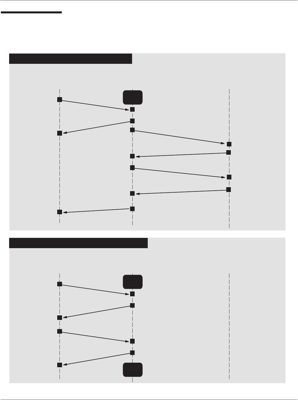
Quick Poll
Sequence
TERMINAL CAD
NORMAL QUICK POLL SEQUENCE
Quick Poll
Request
Quick Poll
Response
DąWait for a command from the Terminal
Wait
Mode
CARD
REQ
ATQ
DąCard in field receives
REQ and returns ATQ
ATTRIB
DąCAD issues ATTRIB to
card containing Slot ID,
etc.
DąCard returns response
ATP (NAD, PUPI, etc.)
DąCard is registered
DąTerminal and card
communicate per
application with CAD
serving as pipeline
TERMINAL CAD
INTERRUPTED QUICK POLL SEQUENCE
Quick Poll
Request
Quick Poll
Response
DąWait for a command from the Terminal
Wait
Mode
CARD
DąWait for first card
registration
Any Frame
Response to
the Frame
DąWait for a command from the Terminal
Wait
Mode
DąREQs sent until ATQ is
returned or any frame is
sent from Terminal
ATTRIB RESP
Chapter 5ąCAD Protocols and Commands
5-33
CAD001-Beta 2
5/26/99
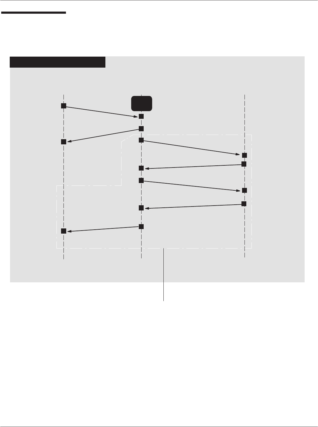
Long Poll
Sequence
TERMINAL CAD
DąProcess antiĆcollision algorithm
DąLog the first detected card
DąSend an ATTRIB command to this card
LONG POLL SEQUENCE
Long Poll
Request
Long Poll
Response
DąWait for a command from the Terminal
Wait
Mode
CARD
DąCard in field receives
REQ and returns ATQ
ATP (NAD, PUPI, etc.)
DąCard is registered
DąTerminal and card
communicate per
application with CAD
serving as pipeline
DąWait for first card
registration
REQ
ATQ
ATTRIB
DąCAD issues ATTRIB to
card containing Slot ID,
etc.
DąCard returns response
DąREQs sent until ATQ is
returned or any frame is
sent from Terminal
ATTRIB RESP
This sequence may be repeated up
to four times (should four cards
be presented at the same time).
Card Acceptance Device (CAD) Technical User's Guide
5-34 CAD001-Beta 2
5/26/99
Detect Card
Sequence
DETECT CARD SEQUENCE
TERMINAL CAD
Detect Card
Request
DąWait for a command from the Terminal
Wait
Mode
CARD
REQ
ATQ
DąCard in field receives
REQ and ruturns ATQ
Card Presence
Request
DąWait for detection
result
DąWait for a command from the Terminal
Wait
Mode
Chapter 5ąCAD Protocols and Commands
5-35
CAD001-Beta 2
5/26/99
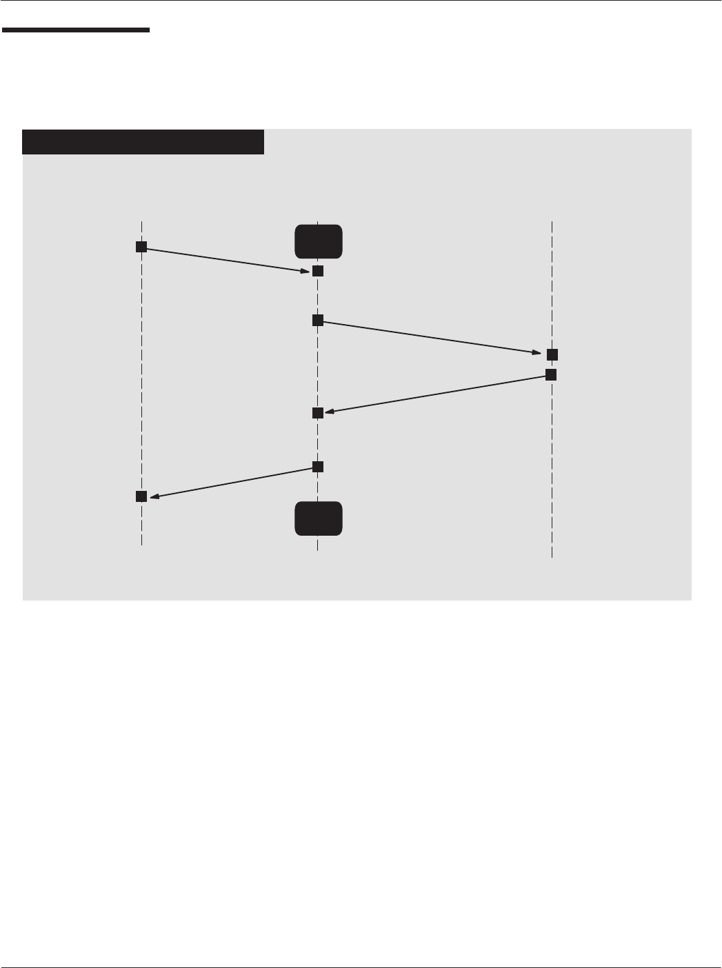
RF Power Control
Sequence
TERMINAL CAD
TURN ON SEQUENCE
Wait
Mode
RF Power
Request
DąWait for a command from the Terminal
RF Power
Response
DąSend RF Power Control
command (parameter 0x00)
Wait
Mode
DąWait for a command from the Terminal
DąTurn on RF power
DąAcknowledge command
TERMINAL CAD
TURN OFF SEQUENCE
Wait
Mode
RF Power
Request
DąWait for a command from the Terminal
RF Power
Response
DąSend RF Power Control
command (parameter 0x01)
Wait
Mode
DąWait for a command from the Terminal
DąTurn off RF power
DąAcknowledge command
Card Acceptance Device (CAD) Technical User's Guide
5-36 CAD001-Beta 2
5/26/99
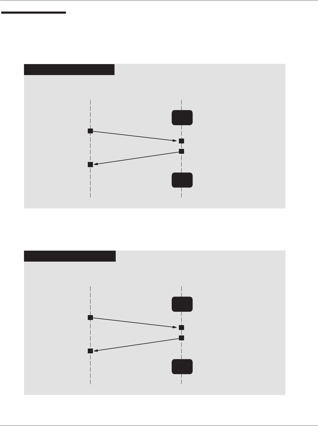
RF Power Control
Sequence
(continued)
TERMINAL CAD
DECREASE POWER SEQUENCE
Wait
Mode
RF Power
Request
DąWait for a command from the Terminal
RF Power
Response
DąSend RF Power Control
command (parameter 0x02)
Wait
Mode
DąWait for a command from the Terminal
DąDecrease RF power
DąAcknowledge command
TERMINAL CAD
INCREASE POWER SEQUENCE
Wait
Mode
RF Power
Request
DąWait for a command from the Terminal
RF Power
Response
DąSend RF Power Control
command (parameter 0x03)
Wait
Mode
DąWait for a command from the Terminal
DąIncrease RF power
DąAcknowledge command
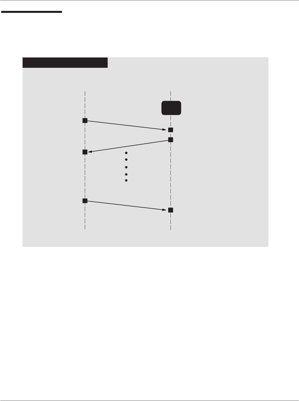
Chapter 5ąCAD Protocols and Commands
5-37
CAD001-Beta 2
5/26/99
Sleep Sequence
TERMINAL CAD
SLEEP SEQUENCE
Wait
Mode
Sleep Request
DąWait for a command from the Terminal
Sleep Response
DąSend Sleep Command
DąAcknowledge command
DąTurn off RF power
DąEnter STOP mode until a frame from
terminal is received
Any Frame
DąExit STOP mode
DąTurn on RF power
DąReceive frame
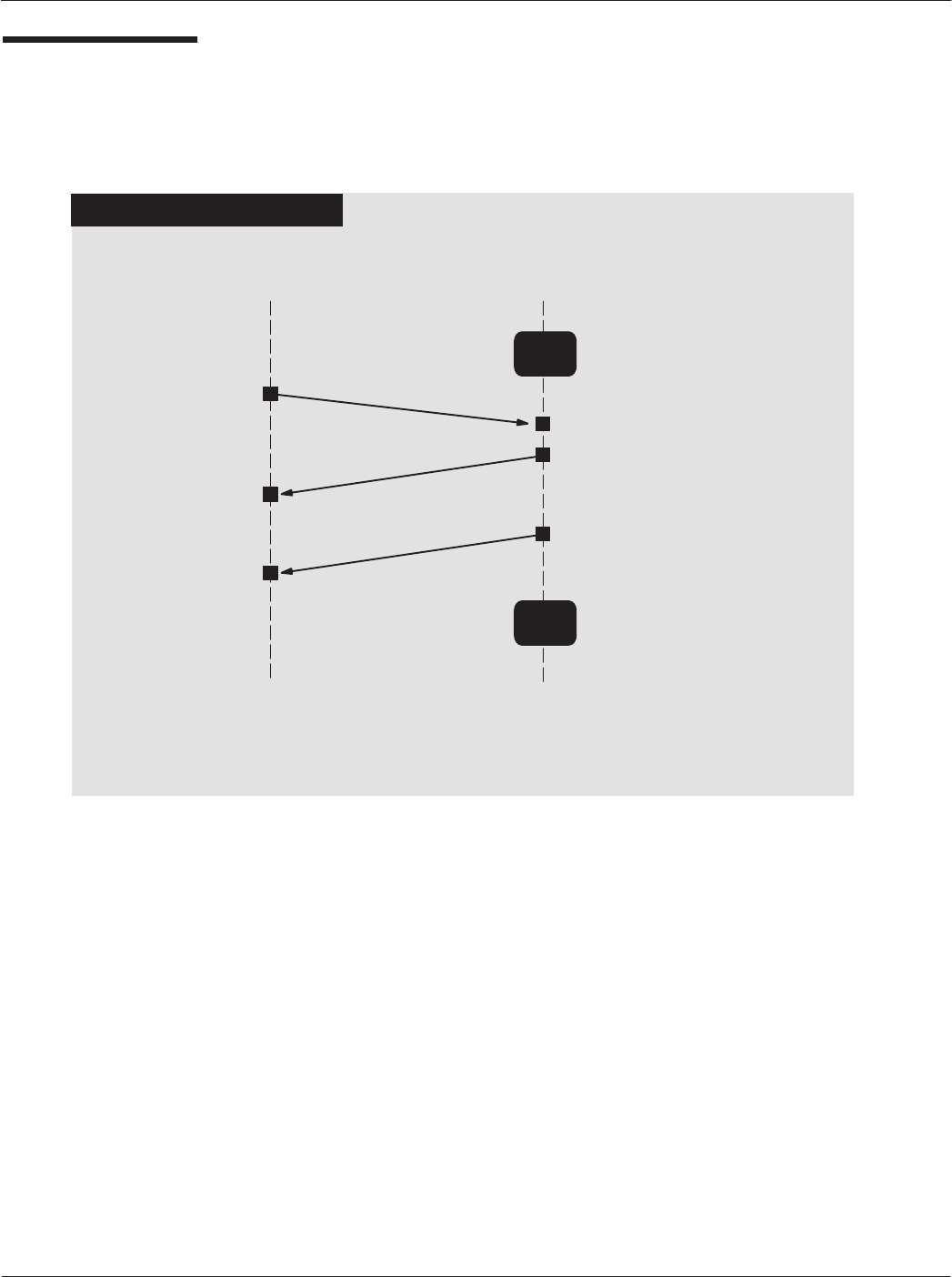
Card Acceptance Device (CAD) Technical User's Guide
5-38 CAD001-Beta 2
5/26/99
Reboot
Sequence
TERMINAL CAD
REBOOT SEQUENCE
Wait
Mode
Reboot Request
DąWait for a command from the Terminal
Reboot Response
DąSend Reboot Command
DąAcknowledge command
DąReset CPU
ATR at 9600 BPS
Wait
Mode
DąWait for a command from the Terminal

Appendix A "Performing FLASH Upgrades
Card Acceptance Device (CAD)
Technical User's Guide
CAD001-Beta 2
5/26/99
chapter contents
FLASH Upgrade Procedure 2

Card Acceptance Device (CAD) Technical User's Guide
A-2 CAD001-Beta 2
5/26/99
1FLASH UPGRADE PROCEDURE
Operating software for the CAD is stored in FLASH memory on the Control Board. The software may
be upgraded (or reinstalled) by using the Firmware Download utility included as part of the CADTools
software program (provided with the <MODEL> CAD Installation Kit).
Preparing for Upgrade
Procedure
Locating CAD Operating Software
The upgrade process installs CAD operating software (stored on
the PC hard disk or floppy diskette) into FLASH memory on the
CAD Control Board. Before you begin the upgrade procedure,
make sure you have available the desired version of CAD software.
It is recommended that you copy this software into the following
location on the PC hard disk:
C:\Program Files\CADTools
(Since the Firmware Upgrade utility automatically looks in this
directory first for CAD operating software, locating the software here
will streamline the process as well as provide one central directory
in which to store all of your CAD operating software versions.)
Setting Up the CAD and PC
Connect the CAD to the PC and launch the CADTools program as
described in Launching the CADTools Software on page 2-8 of this
manual.
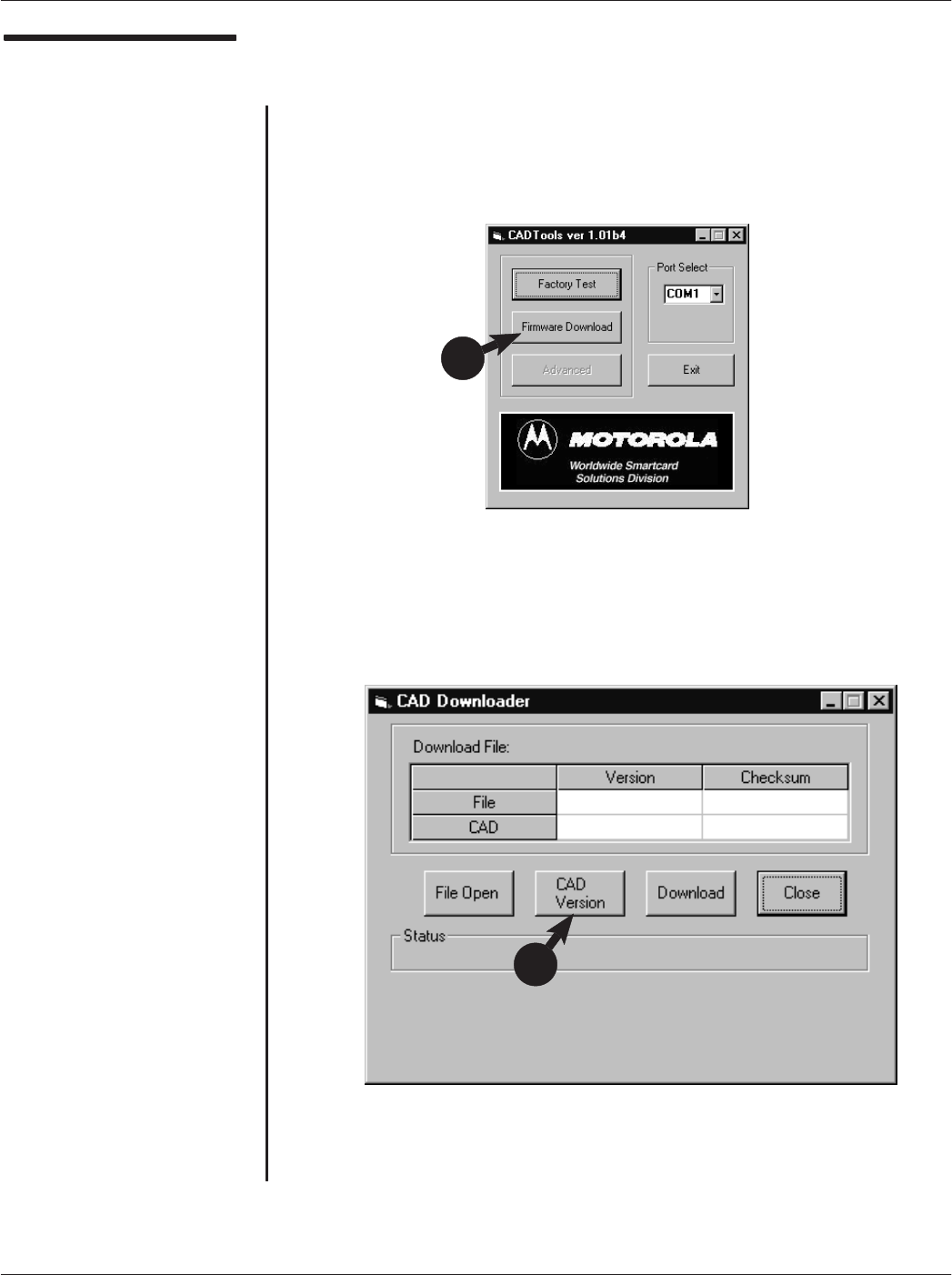
Appendix A Performing FLASH Upgrades
A-3
CAD001-Beta 2
5/26/99
Performing FLASH
Upgrade Procedure
1. With the CAD connected to the PC and the CADTools program
running, click on the Firmware Download button.
2. The following CAD Downloader main screen will appear. Click
on the CAD Version button.
continued on next page
1
2
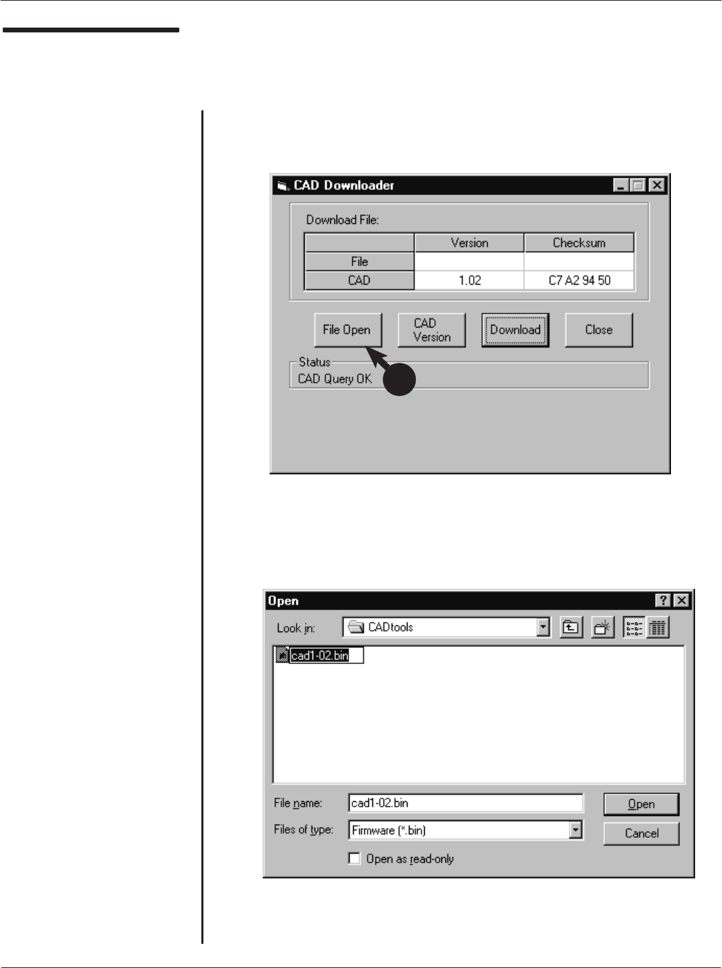
Card Acceptance Device (CAD) Technical User's Guide
A-4 CAD001-Beta 2
5/26/99
Performing FLASH
Upgrade Procedure
(continued)
NoteąYou may have received the
CAD operating software via disĆ
kette, CDĆROM, email, FTP, or other
file transfer means. It is recomĆ
mended that you store all software
files in the default directory (i.e.,
C:\Program Files\CADtools)so
that they will appear in the Open
screen. Otherwise, you will have to
navigate to the file location to select
the desired file.
3. The following screen will appear, displaying the version of CAD
operating software currently in FLASH memory in the CAD. Click
on the File Open button.
4. The following Open screen will appear. You will use this screen to
locate the file containing the CAD operating software you wish to
download to the CAD. Select the desired file and click on Open.
continued on next page
3
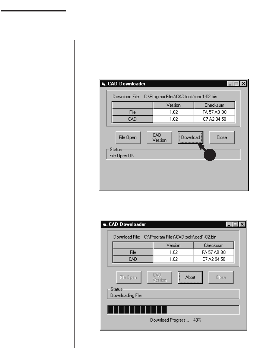
Appendix A Performing FLASH Upgrades
A-5
CAD001-Beta 2
5/26/99
Performing FLASH
Upgrade Procedure
(continued)
5. The following screen will appear, displaying the version of CAD
operating software currently in FLASH memory in the CAD and the
version of the operating software contained in the file you selected
in the previous step. Verify that this is the version you wish to
download to the CAD, then click on the Download button.
6. The following screen will appear, displaying the progress of the
download process.
continued on next page
5
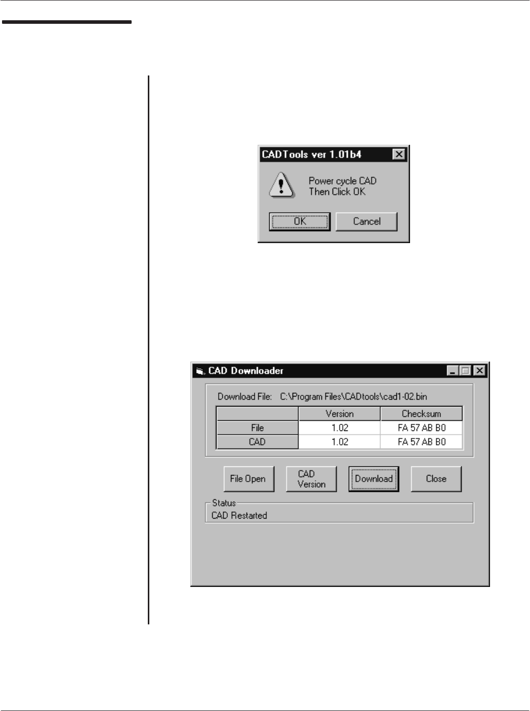
Card Acceptance Device (CAD) Technical User's Guide
A-6 CAD001-Beta 2
5/26/99
Performing FLASH
Upgrade Procedure
(continued)
7. When the download process is complete, the following screen
appears prompting you to power cycle the CAD. Recycle the
CAD power by disconnecting, then reconnecting the black DC
power connector. Then click on OK.
8. The following screen appears. Click on Close. The CAD is now
running the operating software contained in the file you have just
downloaded.
ząEnd of this Procedureąz
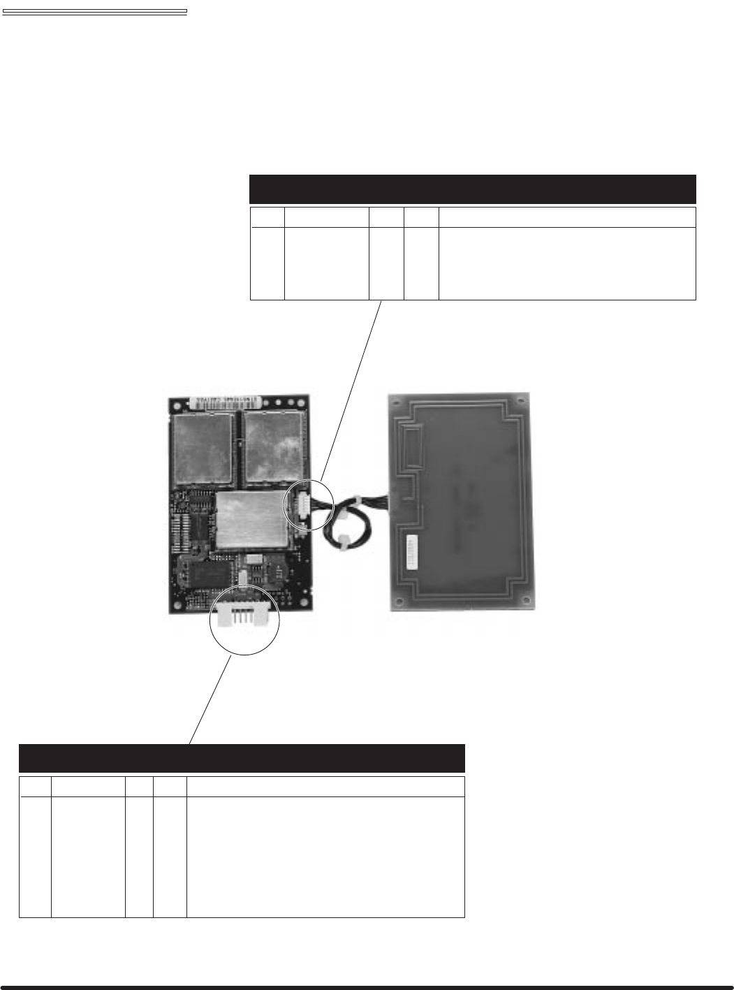
Appendix B "CAD Connector PinĆOuts
Card Acceptance Device (CAD)
Technical User's Guide
CAD001-Beta 2
5/26/99
CONTROL BOARD ANTENNA BOARD
CONNECTOR P4 RS485 TERMINAL CONNECTOR
Pin # Signal Input Output Function
1 NC No Connection
2 GND nGround (Power Supply -VE)
3 +12V nPower Supply VE+ from Terminal
4 RXB nRS485 Serial Data from Terminal to CAD (to be sent to Smart Card)
5 RXA nRS485 Serial Data from Terminal to CAD (to be sent to Smart Card)
6TXB nRS485 Serial Data from CAD to Terminal (received from Smart Card)
7TXA nRS485 Serial Data from CAD to Terminal (received from Smart Card)
8 N/C Future Use
9 GND Ground (Power Supply Negative)
10 N/C Future Use
Pin # Signal Input Output Function
1 ANTENNA_RX Future Use
2 GND nGround
3 GND Ground
4 GND Ground
5 ANTENNA_COIL1 Connects to other end of antenna loop
6 ANTENNA_COIL 1 Connects to other end of antenna loop
CONNECTOR P6 CADĆtoĆANTENNA BOARD
110
6
1

Card Acceptance Device (CAD) Technical User's Guide
B-2 CAD001-Beta 2
5/26/99
Notes...
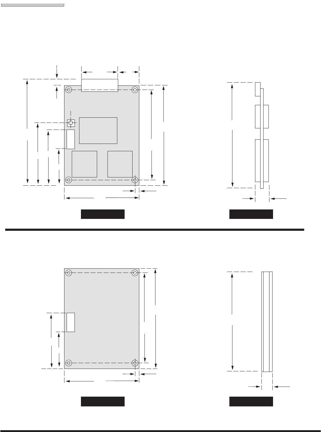
Appendix C "Dimensions and Clearances
Card Acceptance Device (CAD)
Technical User's Guide
CAD001-Beta 2
5/26/99
96
104
4
67
25.15 23
8
112
66
54
TOP VIEW SIDE VIEW
112
13.6
Control Board
96
104
4
67
16.65
TOP VIEW SIDE VIEW
104
4.81
Antenna Board
66
60
All dimensions in millimeters
All dimensions in millimeters
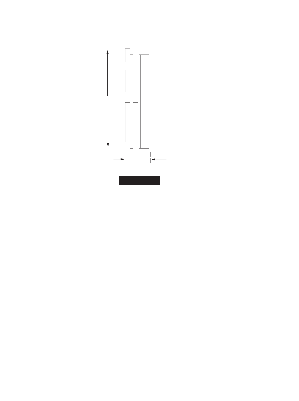
Card Acceptance Device (CAD) Technical User's Guide
C-2 CAD001-Beta 2
5/26/99
SIDE VIEW
Stacked
18.41
112
All dimensions in millimeters

Index
i
CAD001-Beta 2
5/26/99
INDEX
A
ANSWER TO POLL, command, 5-20
Answer to Reset, 5-6
ATR, format, 5-6
B
Boot Sequence, 5-29
BREAK CHARACTER, command, 5-26
C
CAD
major components, 1-2
management commands, 5-8
simplified block diagram, 1-4
typical application, 1-2
CADTools, software
installing, 2-4
launching, 2-8
CARD PRESENCE, command, 5-24
checkout, final, 2-23
command, sequences, 5-28
command protocol, TerminalĆtoĆCAD, 5-2
command sequences, 5-28
commands, CAD management, 5-8
components, CAD
detailed, 1-6
primary, 1-3
D
dc power, verifying, 3-2
DETECT CARD, command, 5-22
Detect Card Sequence, 5-34
download, software, A-3
DOWNLOADING, command, 5-14
Downloading sequence, 5-30
E
epilogue, field, 5-4
equipment, required
for final checkout, 2-23
for Self Test Utility, 2-4
for Tuning, 2-14
ERROR REPORT, command, 5-16
F
fault isolation, procedures, 3-2, 3-3
FLASH, upgrade, procedure, A-3
I
information, field, 5-4
inspecting
CAD, 2-2
CAD sets, 2-2
installing
CAD into terminal, 2-21
CADTools software, 2-4
L
launching, CADTools software, 2-8
LED indicator, verifying, 3-2
Long Poll Sequence, 5-33
M
major components, CAD, 1-2
mounting, into terminal, 2-21
O
operation, verifying proper, 2-4
overview, CAD product, 1-2
P
POLL, command, 5-18

Card Acceptance Device (CAD) Technical User's Guide
ii CAD001-Beta 2
5/26/99
prologue, field, 5-2
Q
Quick Poll Sequence, 5-32
R
REBOOT, command, 5-25
Reboot Sequence, 5-38
RF POWER CONTROL, command, 5-10
RF Power Control Sequence, 5-35
running, Self Test Utility, 2-12
S
Self Test Utility, running, 2-12
SLEEP, command, 5-12
Sleep Sequence, 5-37
T
TerminalĆtoĆCAD, command protocol, 5-2
tuning, procedure, 2-14
typical application, CAD, 1-2
U
unpacking
CAD, 2-2
CAD sets, 2-2