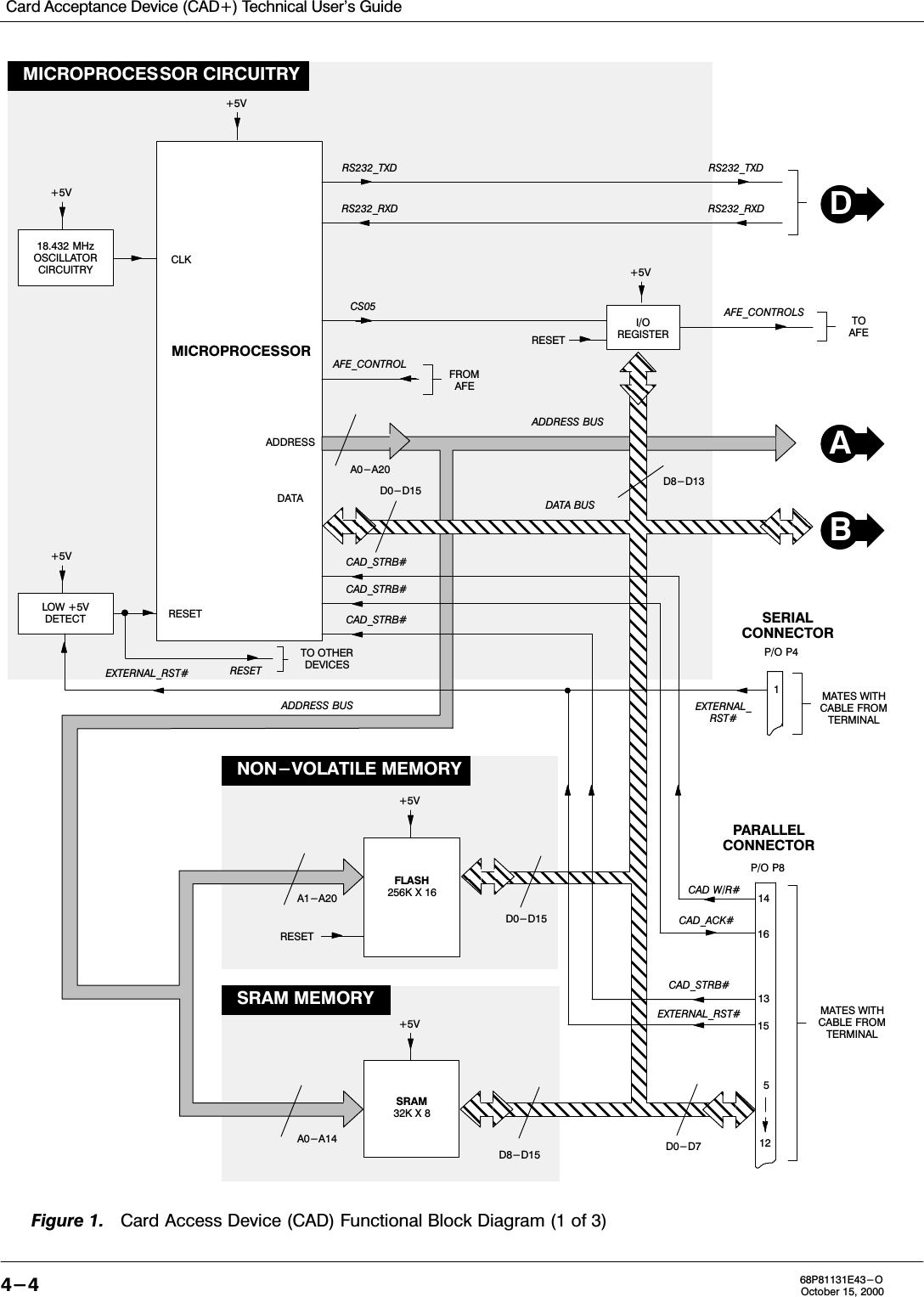
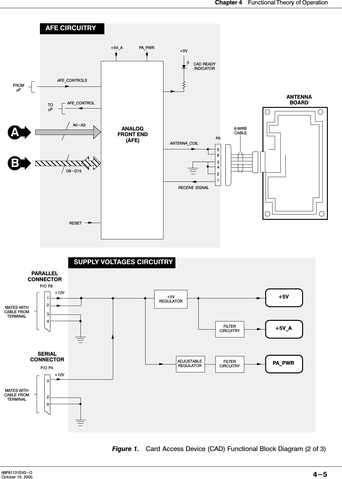
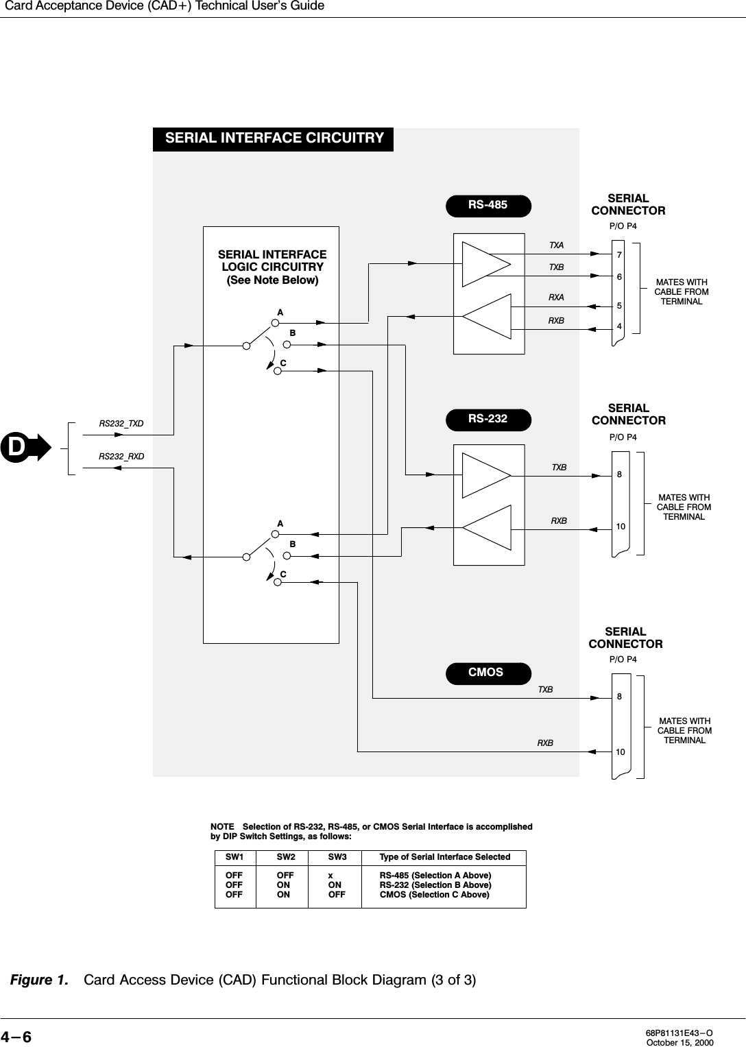
Motorola Solutions MCAD200 Card Acceptance Device User Manual Exhibit 8 Users Manual
Motorola Solutions, Inc. Card Acceptance Device Exhibit 8 Users Manual
UserManual.wiki
>
Motorola Solutions
>
MCAD200 User Manual
User Manual
Navigation menu
Upload a User Manual
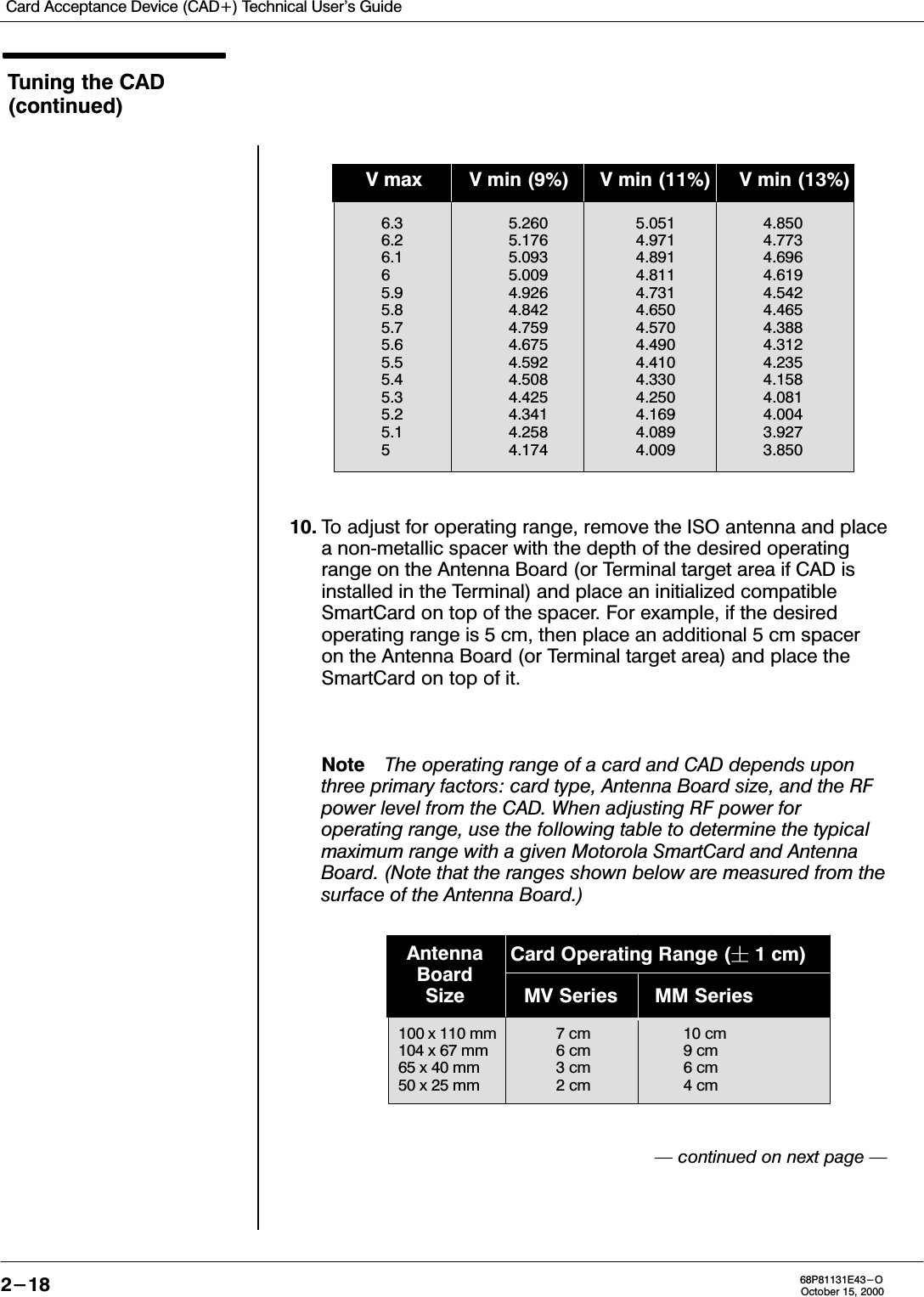
Namespaces
Wiki Guide
HTML
PDF
Info
Views
User Manual
Discussion / Help
Navigation
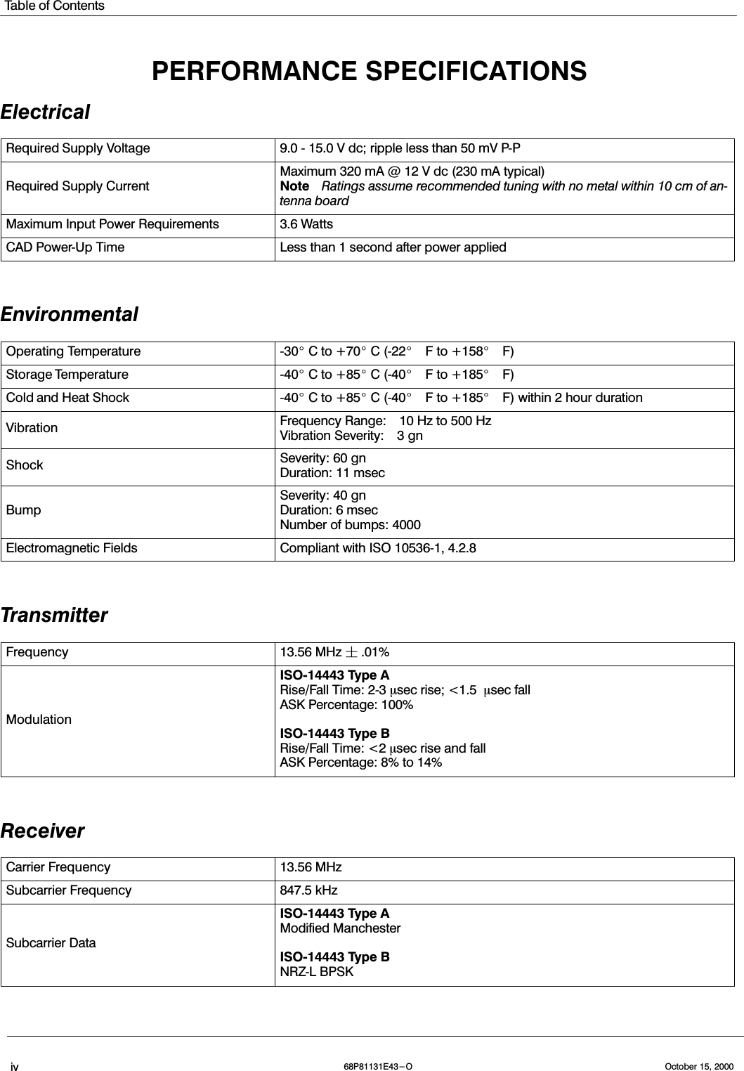
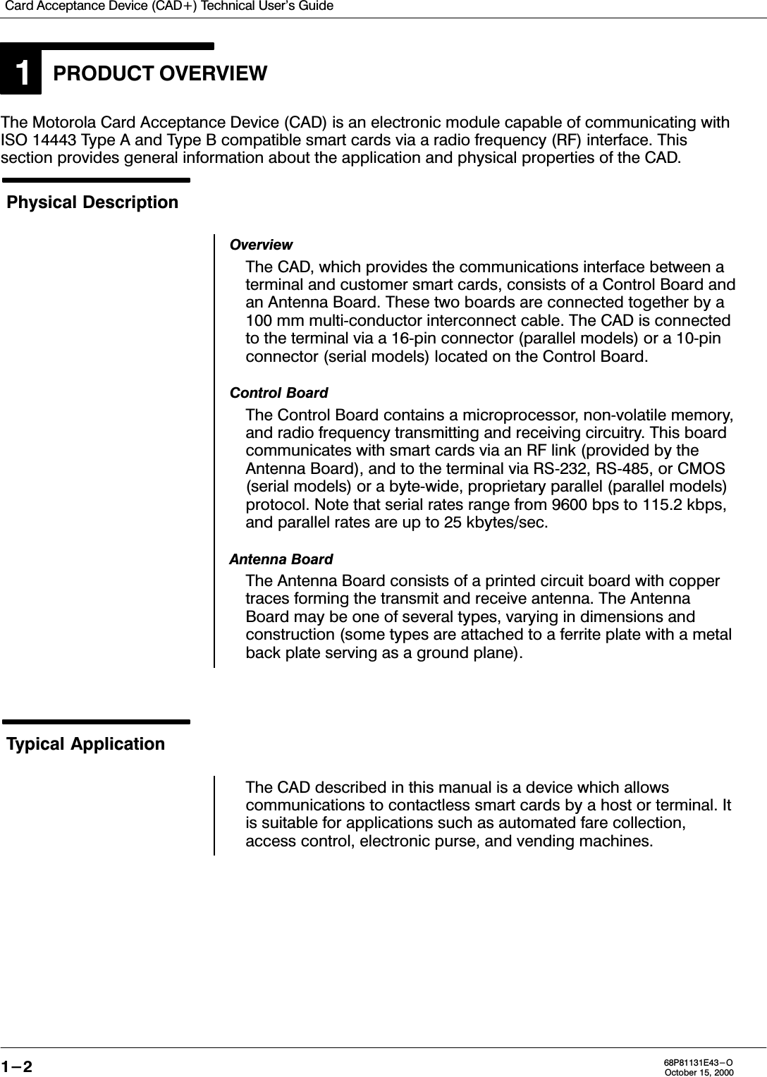

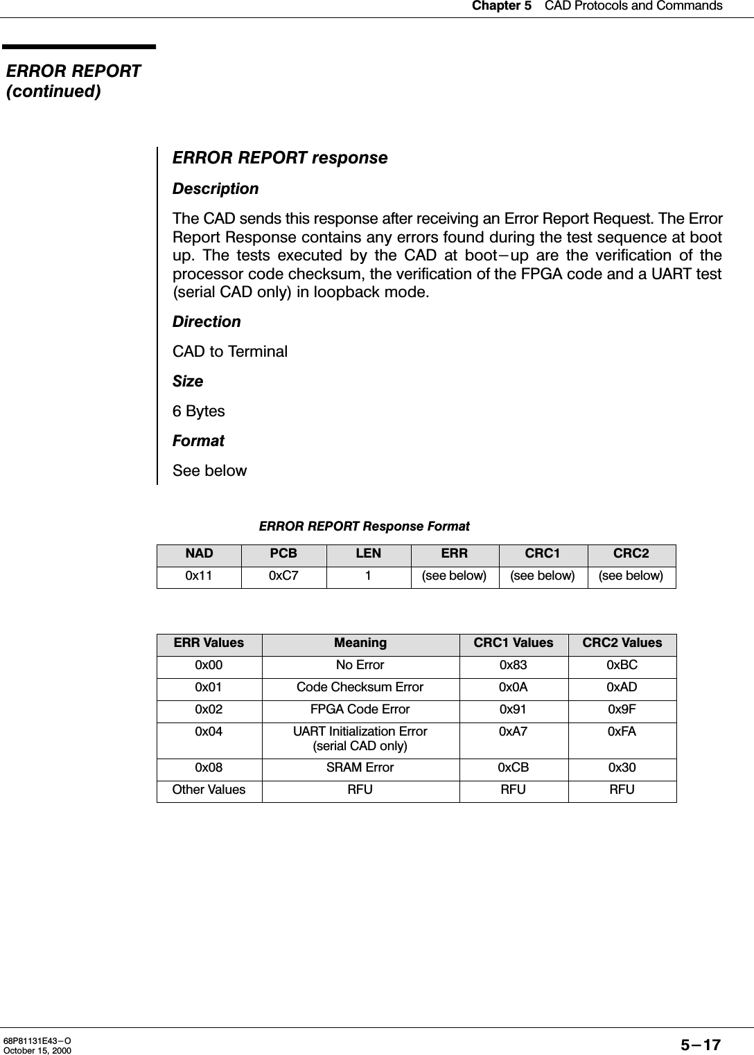
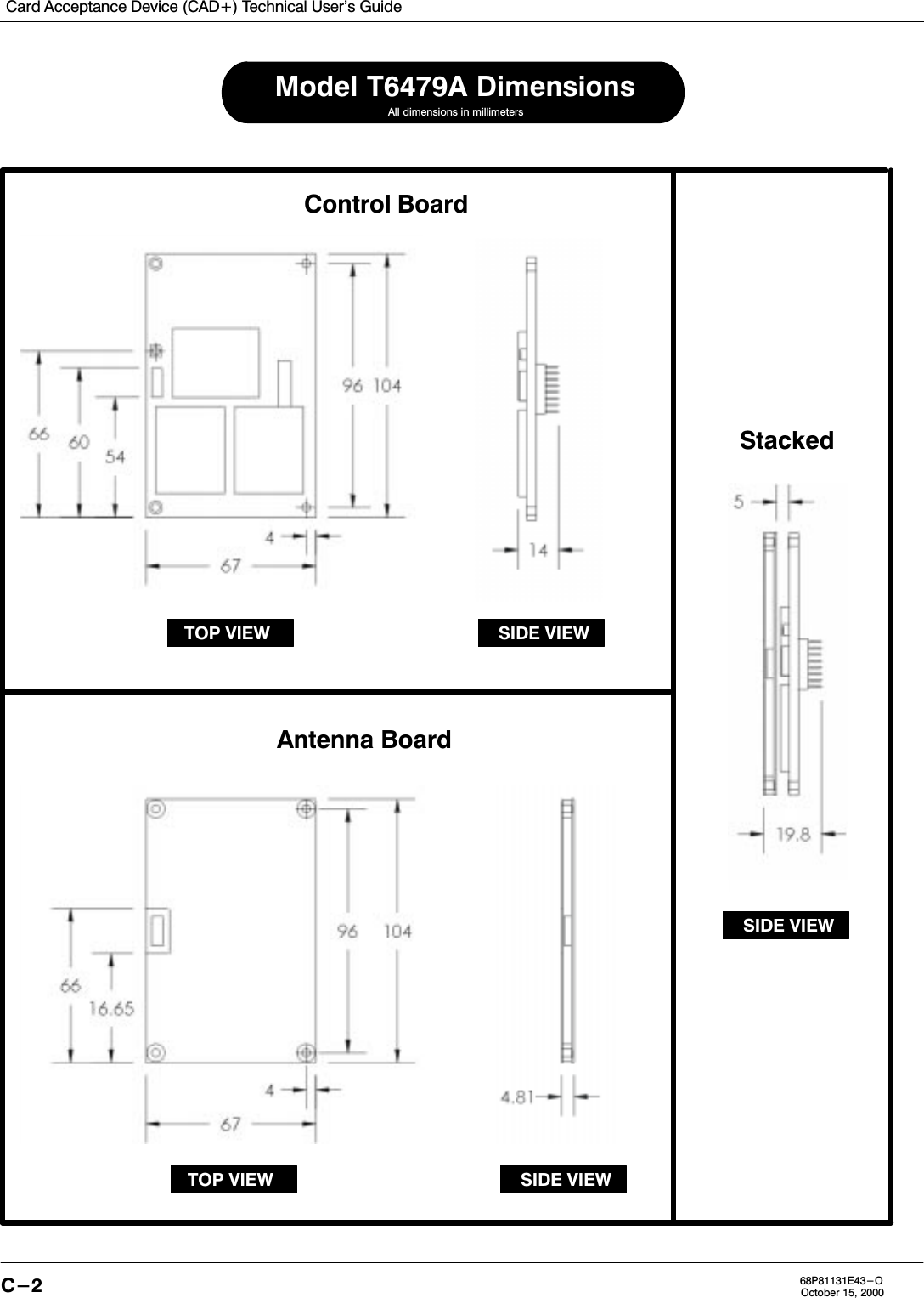
![Chapter 5CAD Protocols and Commands5-768P81131E43-OOctober 15, 2000ATR Format (continued)The four least significant bits of any interface byte TDi indicatesa protocol type T, specifying rules to be used to processtransmission protocols. When TD1 is not transmitted, T=0 isused. TA1 TB1 TC1 and TB2 are the global interface bytes. Theseglobal interface bytes shall be interpreted in order to process anytransmission protocol correctly.The interface characters specify all transmission parameters ofthe current protocol. They are constructed from the bytes TAi,TBi, TCi, and TDi (i =1, 2, 3...). TAi, TBi and TCi indicate theprotocol parameters. Their interpretation depends on theprotocol type indicated by T in TDi-1. TDi indicates the protocoltype T, as defined in [1] Section 6.1.4.3, and the presence ofsubsequent interface characters. The ATR transmission of thesebytes is optional and may be omitted if appropriate.TDi Byte Informationb8 b7 b6 b5 b4 b3 b2 b1 Meaning--- 1 ---- TAi+1 is transmitted--1 ----- TBi+1 is transmitted- 1------ TCi+1 is transmitted1 ------- TDi+1 is transmitted----xxxx Protocol type for subsequent transmissionWhen TDi is not transmitted, the default value of TAi+1 TBi+1TCi+1 is null, indicating that no further interface characters TAi+1TBi+1 TCi+1 TDi+1 will be transmitted. TA1 to TC3 conveyinformation that shall be used during exchanges between theterminal and the CAD subsequent to the Answer to Reset. Theyindicate the values of the transmission control parameters F, D,I, P, and N, and the IFSC, block waiting time integer (BWI), andcharacter waiting time integer (CWI) applicable to T=1 as definedin ISO/IEC 7816-3. The information contained in TA1 to TC1 andTC2 shall apply to all subsequent exchanges.The historical characters, T1 T2 -TK, maximum 15 characters.It designates general information, for example, the CAD firmwareversion.The value of check character TCK shall be such that theexclusive-ORing of all bytes from byte T0 to the last byte beforethe TCK.](https://usermanual.wiki/Motorola-Solutions/MCAD200/User-Guide-122958-Page-62.png)
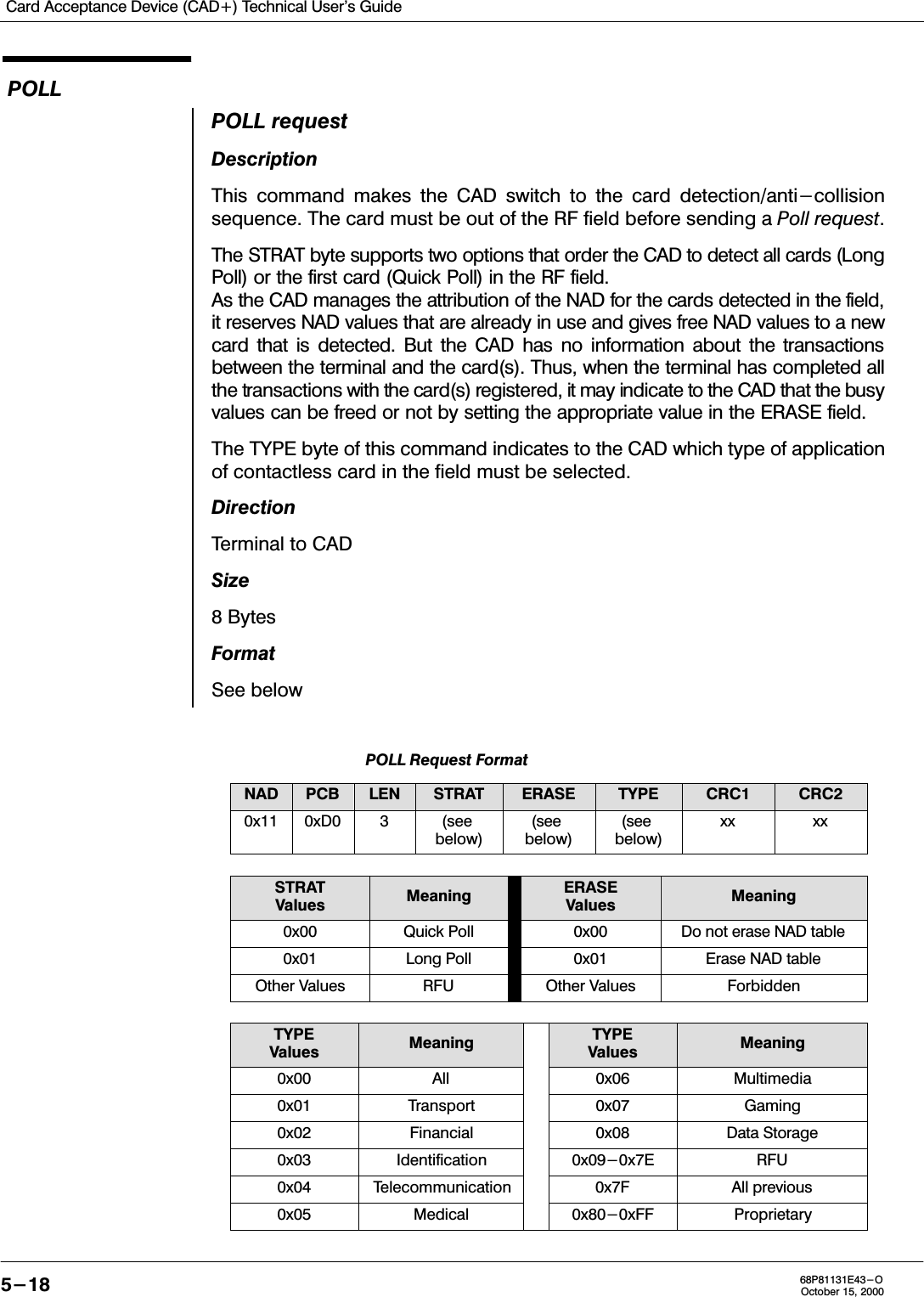
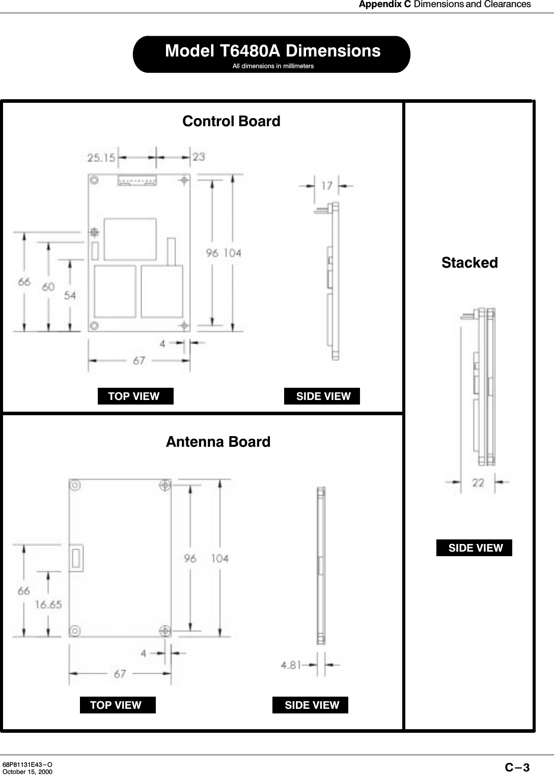
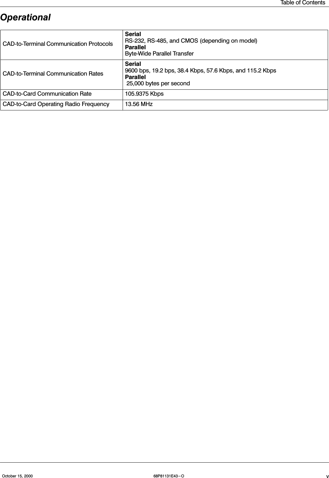
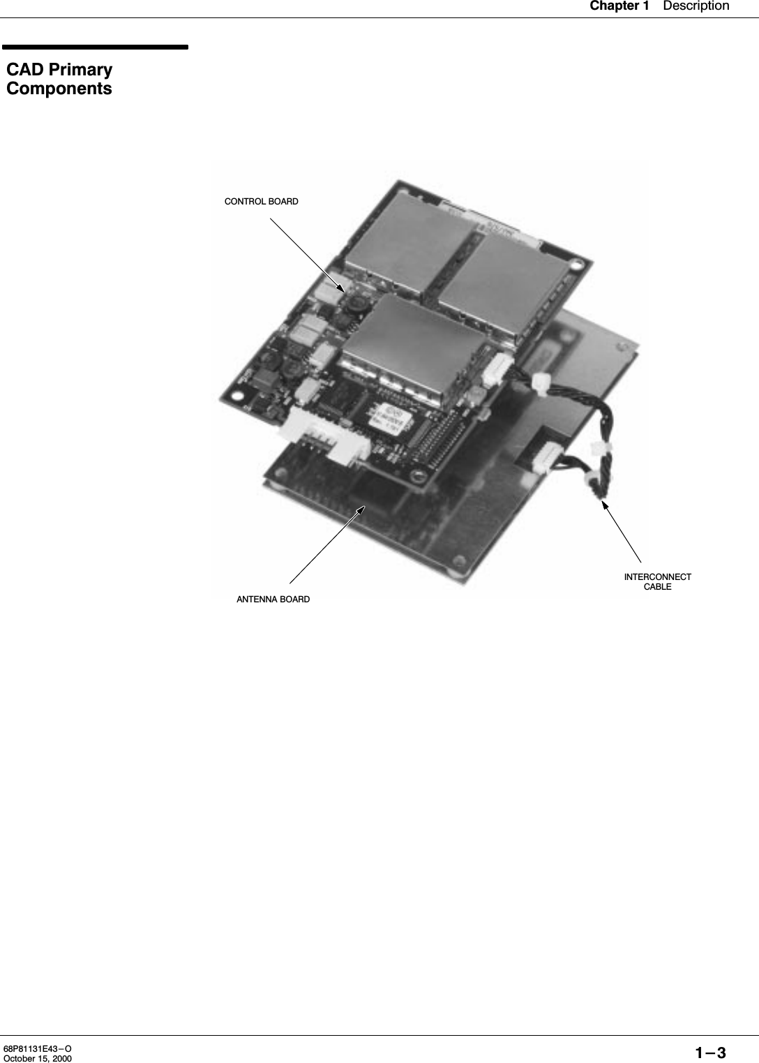
![Card Acceptance Device (CAD+) Technical User's Guide5-8 68P81131E43-OOctober 15, 2000ATR Format (continued)The structure of the ATR is the initial character TS followed by avariable number of subsequent characters in the following order:the format character T0, optionally the interface characters TAi,TBi, TCi, TDi and optionally the historical characters T1 T2 - TKand, conditionally, the check character TCK.ATR Data InformationCharacter Value MeaningTS 3B Indicates direct conventionT0 F3 F = (1111)bin, TA1, TB1, TC1, and TD1 present; 3 indicates the number of historical bytes presentTA171 Most significant half byte (b8 to b5): Default BaudRate (0...7) Least significant half byte (b4 to b1): Di = 1TB100 Vpp is not requiredTC1FF Indicates amount of extra guard time required (FF = no guard time)TD191 9 = (1001)bin, TB2 and TC2 absent; TA2 and TD2present;1 indicates that T=1 is to be usedTA281 specific mode" ; [6]8 = (1000)bin, b8 = 1 mode change not allowed1 indicates that T=1 is to be usedTD271 7 = (0111)bin, TA3, TB3, TC3 present; TD3 absent1 indicates that T=1 is to be usedTA3FF IFSI = FF, which indicates initial value (255 bytes) forinformation field size for the CADTB301 b8-b5 = 0 BWI minimumb4-b1 = 0 CWI minimumTC300 01 = CRC in useT1T2T3XXXX11Version Number of CAD Firmware (MSB)Version Number of CAD Firmware (LSB)NAD used by the CADTCK XX LRC used for Check character](https://usermanual.wiki/Motorola-Solutions/MCAD200/User-Guide-122958-Page-63.png)