MtM Plus Technology M905 M905 User Manual M905 Product Specification v1 0 20161214
MtM Plus Technology Corporation M905 M905 Product Specification v1 0 20161214
Users Manual

All rights are reserved by ASE. No part of this technical document can be reproduced in any form without permission of ASE.
1
Product Specification
of
M905 Bluetooth 4.2 LE SiP Module
Data Sheet-Preliminary Dec 2, 2016 Rev1.0.0
M905 Bluetooth 4.2 LE SiP Module
M905 Product Specification - Preliminary
All rights are reserved by ASE. No part of this technical document can be reproduced in any form without permission of ASE.
2
1 Description
The SiP module M905 is a small size
module with antenna inside. The module
provides full function of Bluetooth 4.2
Low Energy in a tiny module via 52 pins
LGA Foot Print. The M905 module
provides everything required to create
Bluetooth 4.2 Low Energy product with
RF, baseband, MCU, qualified Bluetooth
v4.2 stack and customer application
running on a single IC.
M905 enables ultra-low power
connectivity and basic data transfer for
applications previously limited by the
power consumption, size constraints and
complexity of other wireless standards.
The low power consumption and excellent
radio performance make it the best solution
for OEM /ODM customers who require
embedded Bluetooth 4.2 Low Energy
feature, such as, IP camera, car key, sport
and fitness watch, mouse, led light bulb
etc.
For the software and driver development,
we provide extensive technical document
and reference software code for the system
integration.
Hardware evaluation kit and development
utilities will be released base on listed OS
and processors to OEM customers.
2 Features
l Embedded high performance antenna
l Bluetooth® v4.2 BLE radio technology
l Supports concurrent Bluetooth low
energy/ANT protocol operation
l On-chip NFC tag for Out-of-Band (OOB)
pairing
l Up to +4dBm output power
l -96dBm sensitivity, Bluetooth low energy
l Thread safe and run-time protected
l Event driven API
l 2 data rates (2Mbps/1Mbps)
l PPI - maximum flexibility for power-
efficient applications and code
simplification
l SPI Master/Slave
l Automated power management system
with automatic power management of
each peripheral
l Configurable I/O mapping for analog and
digital I/O
l 3 x Master/Slave SPI
l 2 x Two-wire interface (I²C)
l UART (RTS/CTS)
l 3 x PWM
l AES HW encryption
l Real Time Counter (RTC)
l Digital microphone interface (PDM)
l Antenna On Package (AoP)
l LGA-52 package, 6.5 x 6.5 mm

M905 Product Specification - Preliminary
All rights are reserved by ASE. No part of this technical document can be reproduced in any form without permission of ASE.
3
Revision History
Rev.
Date
Description of change
Approval &
Date
Page
Chap
Change(s)
1.0.0
02/12/’16
All
All
Draft version for Review
Maxim Lin

M905 Product Specification - Preliminary
All rights are reserved by ASE. No part of this technical document can be reproduced in any form without permission of ASE.
4
INDEX
1 Description ..................................................................................................................... 2
2 Feature ........................................................................................................................... 2
3 Block Diagram ............................................................................................................... 5
4 Technical Specification ................................................................................................. 6
4.1 Absolute Maximum Ratings ...................................................................................... 6
4.2 Operation Condition ................................................................................................... 6
4.3 Wireless Specifications .............................................................................................. 6
4.4 Radio Specifications Bluetooth 4.2 Low Energy ....................................................... 6
4.5 AoP Antenna Performance ......................................................................................... 7
4.5.1 Antenna Pattern ....................................................................................................... 8
4.5.2 Antenna Return Loss ............................................................................................... 9
4.5.3 AoP Design Guide ................................................................................. 10.11.12.13
4.6 Power Consumption ................................................................................................. 14
5 Dimensions ............................................................................................................. 15.16
6 Pin Assignments ................................................................................................... 17.18
7 Recommend Footprint ............................................................................................... 19
8 Reference Design Circuit ........................................................................................... 20
9 Recommended Reflow Profile ................................................................................... 21
M905 Product Specification - Preliminary
All rights are reserved by ASE. No part of this technical document can be reproduced in any form without permission of ASE.
6
4 TECHNICAL SPECIFICATION
4.1 Absolute Maximum Ratings
The M905 module has to withstand the operational requirements as listed in the table below
No
Description
Value
Unit
Ratings Over Operating Free-Air Temperature Range
1
Supply voltage
All supply pins
-0.3 to 3.9
V
must have the
same voltage
2
Voltage on any digital pin
-0.3 to 3.9
V
4
Storage temperature range
–40 to 125
°C
5
Bluetooth RF output
4
dBm
4.2 Operation Condition
Power supply for the M905 module will be provided by the host via the power pins
Operating Condition
Min.
Typ.
Max.
VCC
1.7
3.3
3.6
Operating ambient temperature range
-20
°C
70
°C
4.3 Wireless Specifications
The M905 module compliance with the following features and standards
Features
Description
Bluetooth Standards
Bluetooth core v4.2 Low Energy
Antenna Port
Support Single Antenna for Bluetooth
Frequency Band
2.402 – 2.480 GHz
4.4 Radio Specifications Bluetooth 4.2 Low Energy
Features
Description
Frequency Band
2.402– 2.480 GHz (2.4 GHz ISM Band)
Number of selectable Sub channels
40 channels
Modulation
GFSK
Supported rates
<2Mbps
Maximum receive level
-10dBm (with PER <30. 8%)
M905 Product Specification - Preliminary
All rights are reserved by ASE. No part of this technical document can be reproduced in any form without permission of ASE.
7
Parameter
Mode and Conditions
Min.
Typ.
Max.
Unit.
RX sensitivity
-
-92
-
dBm
Maximum input
-
-10
dBm
Frequency range
2402
-
2480
MHz
Output power adjustment
ranger
-20
-
4
dBm
Output power
-
0
-
dBm
Output power variation
-
4
-
dB
4.5 AoP Antenna Performance
Items
Freq. band
Gain
Return Loss
VSWR
Spec.
2.4~2.5GHz
>-5 dBi
<-6dB
3 max
Items
Impedance
Polarization
Directivity
Efficiency
Spec.
50 ohm
Linear
Omni-directional
>30%
M905 Product Specification - Preliminary
All rights are reserved by ASE. No part of this technical document can be reproduced in any form without permission of ASE.
8
4.5.1 Antenna Pattern
Omnidirectional Radiation (Center Edge)
!
a. x-Axias!H-Polarization!&!V-Polarization!
!
b. y-Axias!H-Polarization!&!V-Polarization!
!
c. z-Axias!H-Polarization!&!V-Polarization!
M905 Product Specification - Preliminary
All rights are reserved by ASE. No part of this technical document can be reproduced in any form without permission of ASE.
9
!
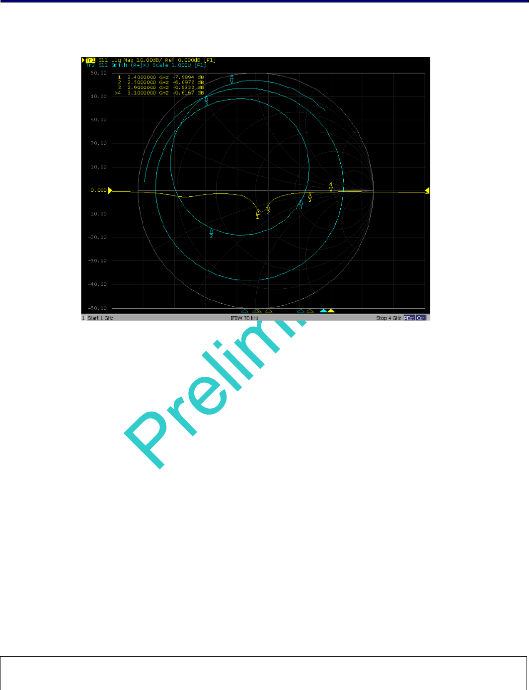
4.5.2 Antenna Return Loss:
!
!
!
!
!
!
!
!
!
!
!
!
!
!
!
!
!
!
!
!
!
!
!
!
!
!
M905 Product Specification - Preliminary
All rights are reserved by ASE. No part of this technical document can be reproduced in any form without permission of ASE.
10
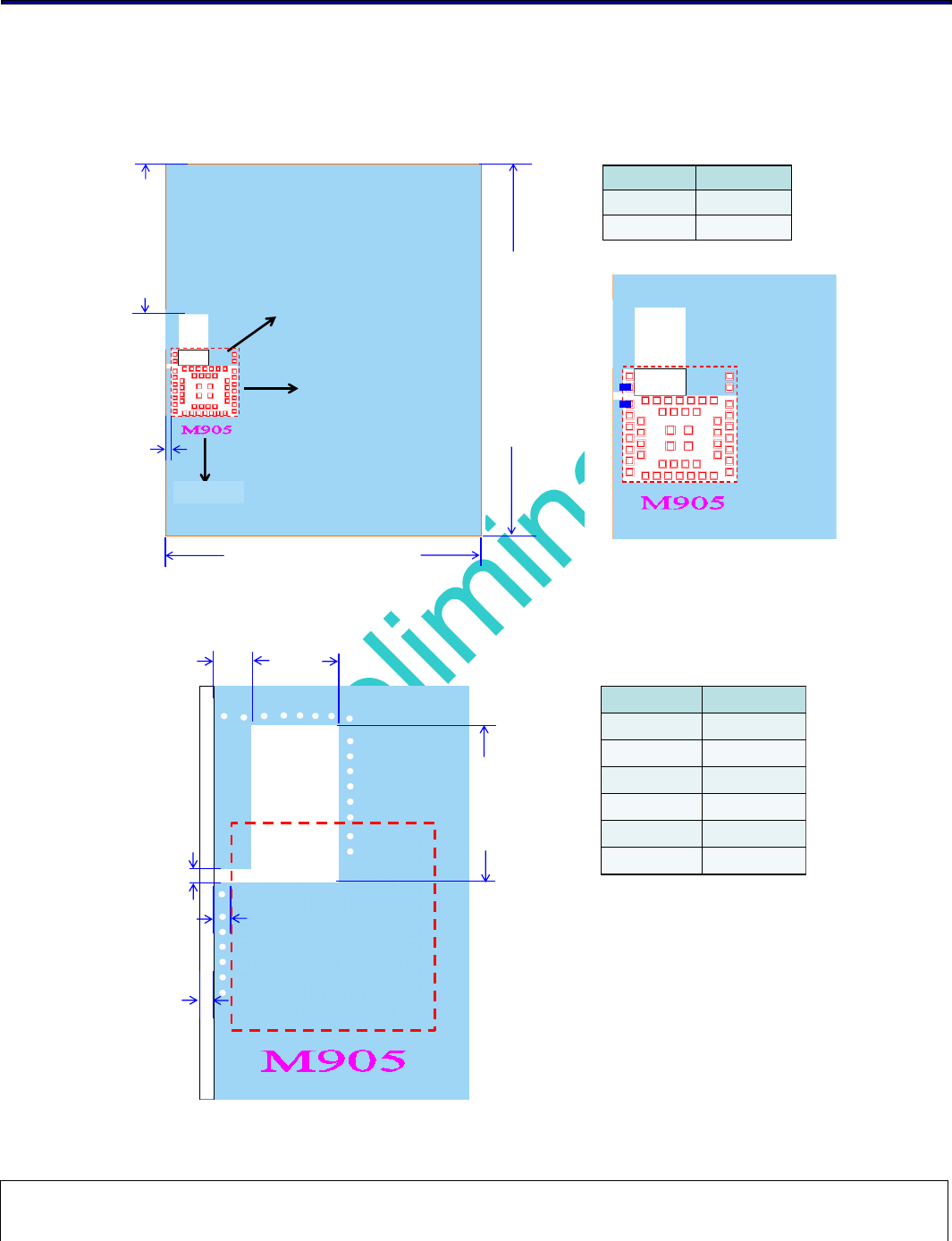
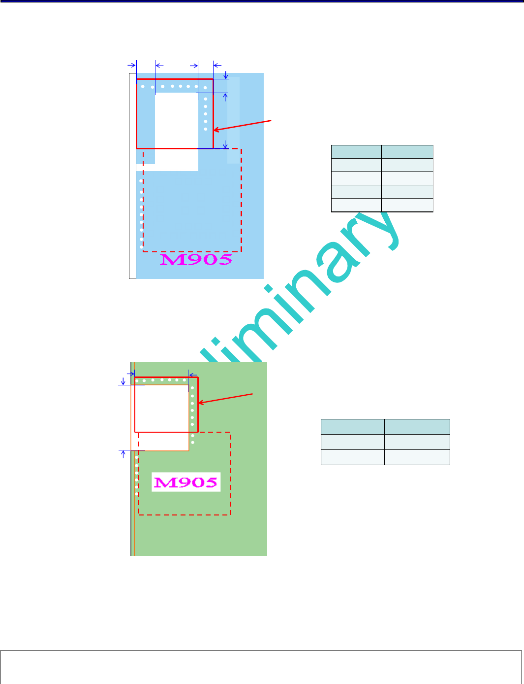
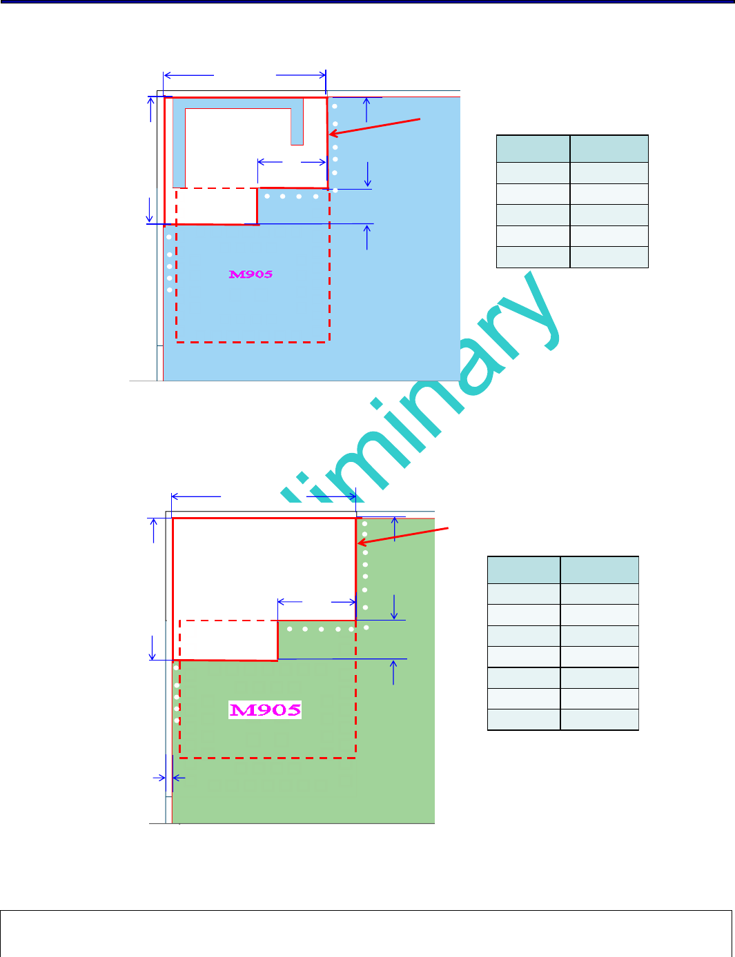
4.5.3 Antenna Design Guide
Center Edge:
a. Keep A≧10.5mm, B≧0.55mm
b. Connect Pin 2 to Upper GND, Pin 3 to lower GND
c. Don’t route signal trace across antenna clearance area
Parameter
Units : mm
A
≧
10.5
B
0.55
A
Trace'route
Trace'route
Trace'route
36mm
31mm
B
Pin2
Pin3
Layer 1
Layer 1
CD
E
Parameter
Units : mm
C
1.25
D
2.9
E
5
F
0.38
G
0.55
H
0.25
Layer 1
F
H
G
M905 Product Specification - Preliminary
All rights are reserved by ASE. No part of this technical document can be reproduced in any form without permission of ASE.
11
Parameter
Units : mm
I
1.25
J
0.5
K
0.5
L
3.5
Layer 1
Antenna Clearance Area
IJ
L
Upper(GND
Lower((GND
K
N
M
Parameter
Units : mm
M
4.15
N
5
Layer 2,3,4
Antenna Clearance Area
M905 Product Specification - Preliminary
All rights are reserved by ASE. No part of this technical document can be reproduced in any form without permission of ASE.
12
Coner :
a. Connect Pin 1 to Ant. trace
b. Don’t route signal trace across antenna clearance area
Layer 1
31mm
36mm
Ant.)Trace
Trace)route
Trace)route
Trace)route
Pin1
Layer 1
G
F
I
K
E
Parameter
Units : mm
A
0.5
B
4.34
C
0.5
D
1
E
1
F
2
G
1.5
H
0.29
I
3.5
J
0.25
K
0.25
Layer 1
H
J
A
BCD
M905 Product Specification - Preliminary
All rights are reserved by ASE. No part of this technical document can be reproduced in any form without permission of ASE.
13
Parameter
Units : mm
L
6.75
M
3.5
N
1.5
O
2.9
P
5
O
L
N
M
P
Layer 1
Antenna Clearance Area
Parameter
Units : mm
J
6.75
K
0.25
L
3.75
M
5
N
4.1
O
5.25
P
0.25
Layer 2,3,4
K
J
P
L
M
M
Antenna Clearance Area

M905 Product Specification - Preliminary
All rights are reserved by ASE. No part of this technical document can be reproduced in any form without permission of ASE.
14
4.6 Power Consumption
Item
Condition
Typ.
Tx mode
3.3V
12.06
1.8V
Rx mode
3.3V
15.32
1.8V
System ON
Constant Latency
Sleep Mode
M905 Product Specification - Preliminary
All rights are reserved by ASE. No part of this technical document can be reproduced in any form without permission of ASE.
15
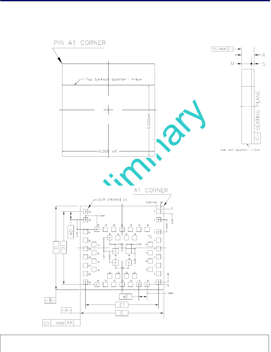
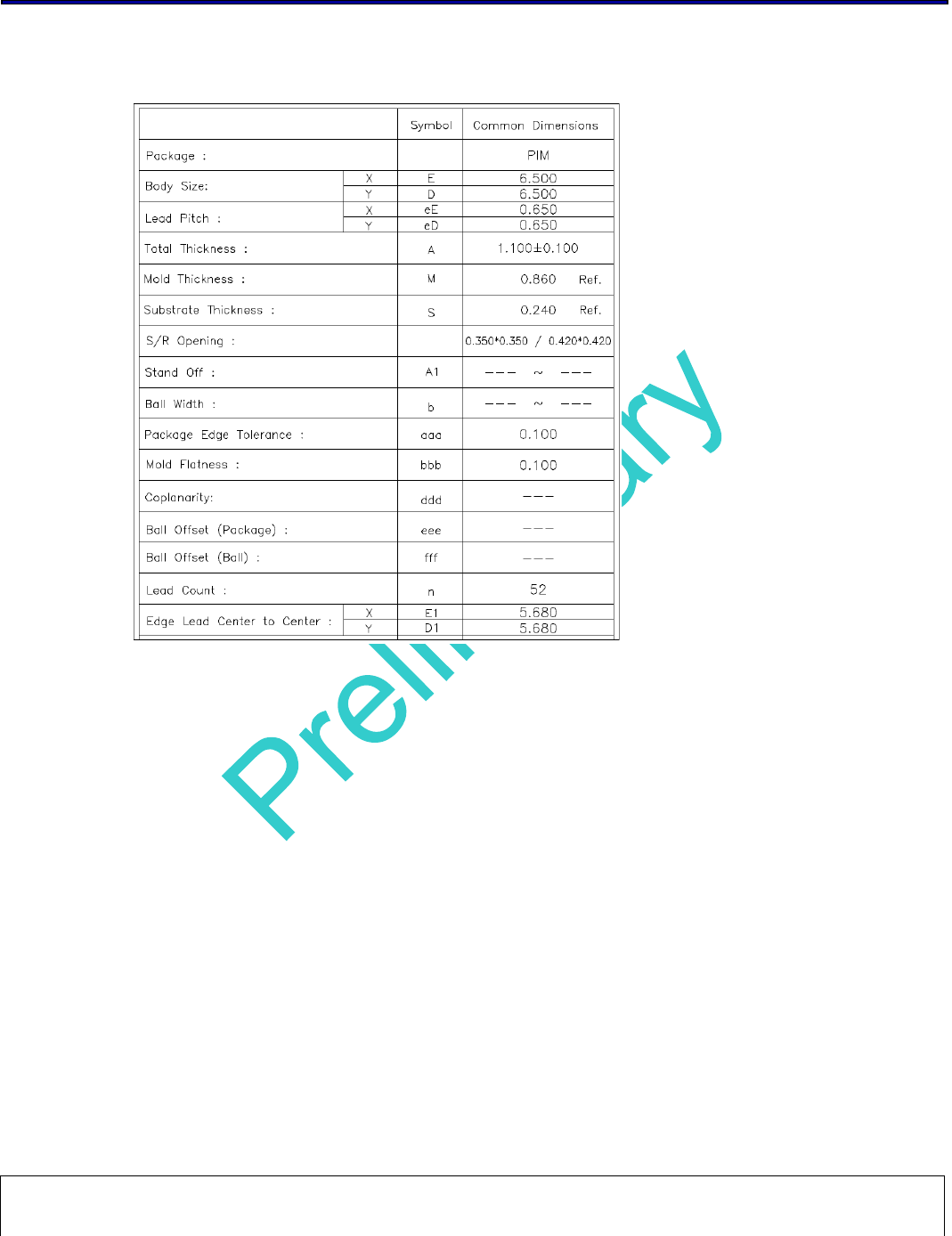
5. Dimensions
The size and thickness of the M905 module 6.5mm (W) x 6.5mm (L) x 1.3mm (H):
Top-View:
Side-View:
Bottom-View:
M905 Product Specification - Preliminary
All rights are reserved by ASE. No part of this technical document can be reproduced in any form without permission of ASE.
16
Dimensions

M905 Product Specification - Preliminary
All rights are reserved by ASE. No part of this technical document can be reproduced in any form without permission of ASE.
17
6. PIN DEFINITION
The foot print dimension and pin definition is defined as below
No
Pin Name
Pin Type
Description
1!
Antenna!Leg!
RF!
Scenario!B!
2!
GNDA1!
RF!
Scenario!A!
3!
GNDA2!
RF!
Scenario!A!
4!
GND!
Power!
Ground!(0V)!
5!
ANT!
RF!
Single-endded!radio!antenna!connection!
6!
RF!
RF!
Single-endded!radio!antenna!connection!
7!
GND!
Power!
Ground!(0V)!
8!
GND!
Power!
Ground!(0V)!
9!
VDD!
Power!
Power!supply!
10!
GND!
Power!
Ground!(0V)!
11!
GND!
Power!
Ground!(0V)!
12!
P0.21/nRESET!
Digital!I/O!
General!purpose!I/O!pin.!Configurable!as!system!
RESET!pin!
13!
P0.14/TRACEDATA[3]!
Digital!I/O!
General!purpose!I/O!pin.!Trace!port!output!
14!
P0.15/TRACEDATA[2]!
Digital!I/O!
General!purpose!I/O!pin.!Trace!port!output!
15!
P0.16/TRACEDATA[1]!
Digital!I/O!
General!purpose!I/O!pin.!Trace!port!output!
16!
P0.18/TRACEDATA[0]!
Digital!I/O!
General!purpose!I/O!pin.!Trace!port!output!
17!
P0.00/XL1!
Digital!I/O!
Analog!input!
General!purpose!I/O!pin.!Connection!for!32.768kHz!
crystal!(LFXO)!
18!
P0.01/XL2!
Digital!I/O!
Analog!input!
General!purpose!I/O!pin.!Connection!for!32.768kHz!
crystal!(LFXO)!
19!
P0.03/AIN1!
Digital!I/O!
Analog!input!
General!purpose!I/O!pin.!SAADC/COMP/LPCOMP!
input!
20!
P0.02/AIN0!
Digital!I/O!
Analog!input!
General!purpose!I/O!pin.!SAADC/COMP/LPCOMP!
input!
21!
P0.09/NFC1!
Digital!I/O!NFC!
input!
General!purpose!I/O!pin.!NFC!antenna!connection!
22!
P0.10/NFC2!
Digital!I/O!NFC!
input!
General!purpose!I/O!pin.!NFC!antenna!connection!
23!
P0.05/AIN3!
Digital!I/O!
Analog!input!
General!purpose!I/O!pin.!SAADC/COMP/LPCOMP!
input!
24!
P0.04/AIN2!
Digital!I/O!
Analog!input!
General!purpose!I/O!pin.!SAADC/COMP/LPCOMP!
input!
25!
P0.31/AIN7!
Digital!I/O!
Analog!input!
General!purpose!I/O!pin.!SAADC/COMP/LPCOMP!
input!
26!
P0.30/AIN6!
Digital!I/O!
Analog!input!
General!purpose!I/O!pin.!SAADC/COMP/LPCOMP!
input!
27!
P0.29/AIN5!
Digital!I/O!
Analog!input!
General!purpose!I/O!pin.!SAADC/COMP/LPCOMP!
input!
28!
P0.28/AIN4!
Digital!I/O!
Analog!input!
General!purpose!I/O!pin.!SAADC/COMP/LPCOMP!
input!
29!
P0.27!
Digital!I/O!
General!purpose!I/O!pin!
30!
P0.25!
Digital!I/O!
General!purpose!I/O!pin!
31!
P0.26!
Digital!I/O!
General!purpose!I/O!pin!

M905 Product Specification - Preliminary
All rights are reserved by ASE. No part of this technical document can be reproduced in any form without permission of ASE.
18
No
Pin Name
Pin Type
Description
32!
GND!
Power!
Ground!(0V)!
33!
GND!
Power!
Ground!(0V)!
34
P0.11
Digital I/O
General purpose I/O pin
35
P0.19
Digital I/O
General purpose I/O pin
36
P0.22
Digital I/O
General purpose I/O pin
37
P0.23
Digital I/O
General purpose I/O pin
38
P0.24
Digital I/O
General purpose I/O pin
39
SWDCLK
Digital input
Serial wire debug clock input for debug and
programming
40
SWDIO
Digital I/O
Serial wire debug I/O for debug and programming
41
GND
Power
Ground (0V)
42
GND
Power
Ground (0V)
43
GND
Power
Ground (0V)
44
GND
Power
Ground (0V)
45
P0.20/TRACECLK
Digital I/O
General purpose I/O pin. Trace port clock output
46
GND
Power
Ground (0V)
47
GND
Power
Ground (0V)
48
GND
Power
Ground (0V)
49
GND
Power
Ground (0V)
50
GND
Power
Ground (0V)
51
GND
Power
Ground (0V)
52
GND
Power
Ground (0V)
M905 Product Specification - Preliminary
All rights are reserved by ASE. No part of this technical document can be reproduced in any form without permission of ASE.
19
7. RECOMMEND FOOTPRINT
SMD Design:
M905 Product Specification - Preliminary
All rights are reserved by ASE. No part of this technical document can be reproduced in any form without permission of ASE.
21
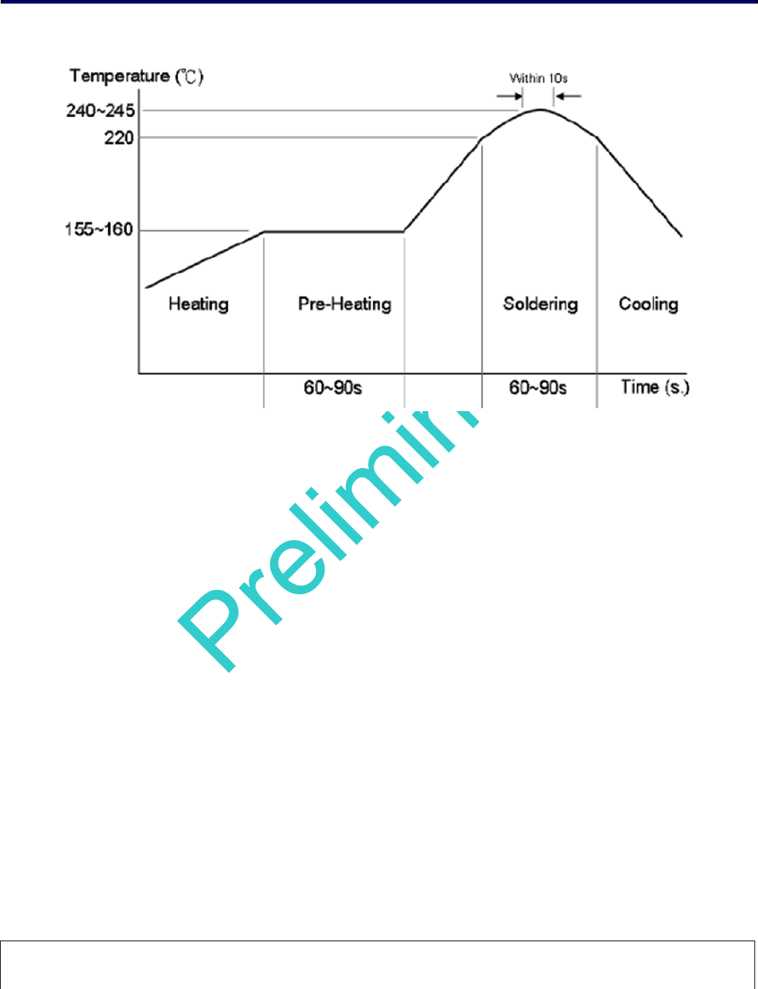
9. RECOMMEND REFLOW PROFILE
Profile Condition
a. Suitable for Lead-Free solder
b. Between 155~160°C: 60~90 sec.
c. Above 220°C: 60~90 sec.
d. Peak Temperature: 240~245 (<10 sec.)
Federal Communication Commission Interference Statement
This equipment has been tested and found to comply with the limits for a Class B
digital device, pursuant to Part 15 of the FCC Rules. These limits are designed to
provide reasonable protection against harmful interference in a residential
installation. This equipment generates, uses and can radiate radio frequency energy
and, if not installed and used in accordance with the instructions, may cause harmful
interference to radio communications. However, there is no guarantee that
interference will not occur in a particular installation. If this equipment does cause
harmful interference to radio or television reception, which can be determined by
turning the equipment off and on, the user is encouraged to try to correct the
interference by one or more of the following measures:
Reorient or relocate the receiving antenna.
Increase the separation between the equipment and receiver.
Connect the equipment into an outlet on a circuit different fromthat to which the
receiver is connected.
Consult the dealer or an experienced radio/TV technician for help.
FCC Caution: Any changes or modifications not expressly approved by the party
responsible for compliance could void the user's authority to operate this
equipment.
This device complies with Part 15 of the FCC Rules. Operation is subject to the
following two conditions: (1) This device may not cause harmful interference, and (2)
this device must accept any interference received, including interference that may
cause undesired operation.
This device and its antenna(s) must not be co-located or operating in conjunction
with any other antenna or transmitter.
IMPORTANT NOTE:
FCC Radiation Exposure Statement:
This equipment complies with FCC radiation exposure limits set forth for an
uncontrolled environment. This equipment should be installed and operated with
minimum distance 20cm between the radiator & your body.
IMPORTANT NOTE:
This module is intended for OEM integrator. The OEM integrator is still responsible
for the FCC compliance requirement of the end product, which integrates this
module.
Appropriate measurements (e.g. 15 B compliance) and if applicable additional
equipment authorizations (e.g. Verification , Doc) of the host device to be addressed
by the integrator/manufacturer.
IMPORTANT NOTE:
This module is intended for OEM integrator. The OEM integrator is still responsible
for the FCC compliance requirement of the end product, which integrates this
module.
20cm minimum distance has to be able to be maintained between the antenna and
the users for the host this module is integrated into. Under such configuration, the
FCC radiation exposure limits set forth for an population/uncontrolled environment
can be satisfied.
Any changes or modifications not expressly approved by the manufacturer could void
the user's authority to operate this equipment.
USERS MANUAL OF THE END PRODUCT:
In the users manual of the end product, the end user has to be informed to keep at
least 20cm separation with the antenna while this end product is installed and
operated. The end user has to be informed that the FCC radio-frequency exposure
guidelines for an uncontrolled environment can be satisfied. The end user has to also
be informed that any changes or modifications not expressly approved by the
manufacturer could void the user's authority to operate this equipment. If the size of
the end product is smaller than the palm of the hand, then additional FCC part 15.19
statement is required to be available in the users manual: This device complies with
Part 15 of FCC rules. Operation is subject to the following two conditions: (1) this
device may not cause harmful interference and (2) this device must accept any
interference received, including interference that may cause undesired operation.
LABEL OF THE END PRODUCT:
The final end product must be labeled in a visible area with the following " Contains
TX FCC ID: 2AJ9P-M905". If the size of the end product is larger than the palm of the
hand, then the following FCC part 15.19 statement has to also be available on the
label: This device complies with Part 15 of FCC rules. Operation is subject to the
following two conditions: (1) this device may not cause harmful interference and (2)
this device must accept any interference received, including interference that may
cause undesired operation.