Multi Tech Systems 92U08D07823 GSM/GPRS Modem User Manual User Guide
Multi Tech Systems Inc GSM/GPRS Modem User Guide
UserManual.wiki
>
Multi Tech Systems
>
92U08D07823 User Manual
User Guide
Navigation menu
Upload a User Manual
Namespaces
Wiki Guide
HTML
PDF
Info
Views
User Manual
Discussion / Help
Navigation

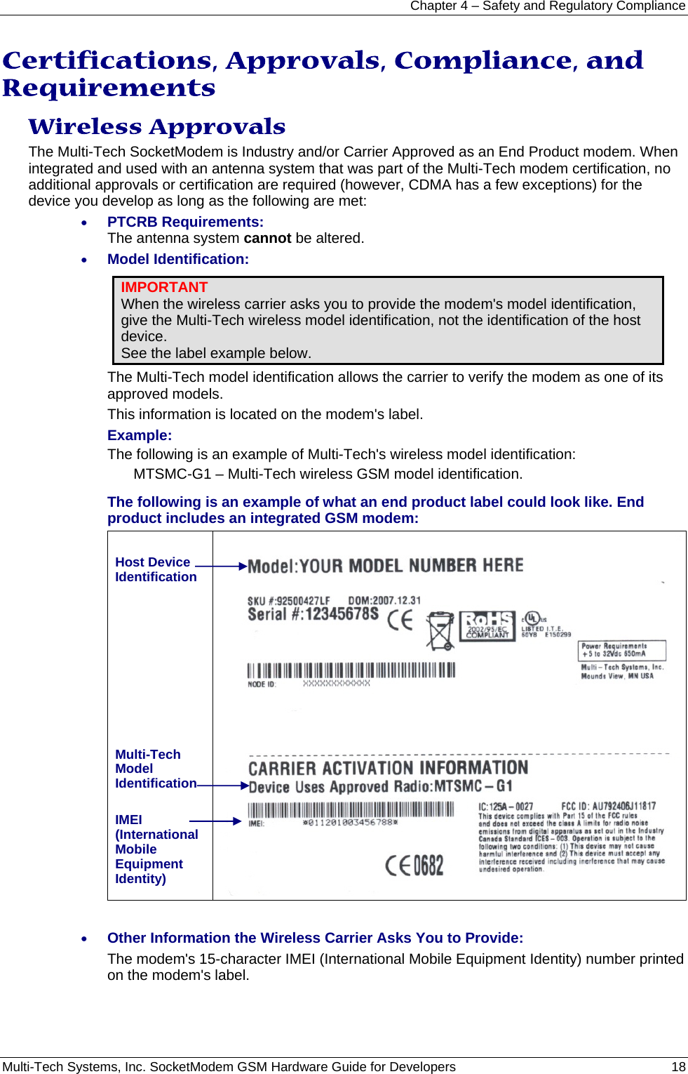
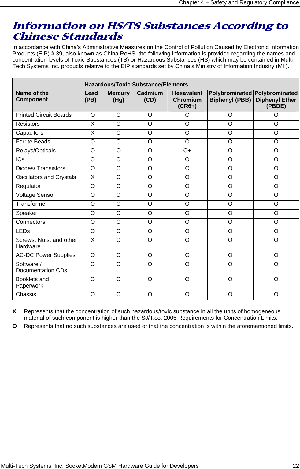
![Chapter 4 – Safety and Regulatory Compliance Multi-Tech Systems, Inc. SocketModem GSM Hardware Guide for Developers 21 Restriction of the Use of Hazardous Substances (RoHS) Multi-Tech Systems, Inc. Certificate of Compliance 2002/95/EC Multi-Tech Systems Inc. confirms that its embedded products now comply with the chemical concentration limitations set forth in the directive 2002/95/EC of the European Parliament (Restriction Of the use of certain Hazardous Substances in electrical and electronic equipment - RoHS) These Multi-Tech Systems, Inc. products do not contain the following banned chemicals: Lead, [Pb] < 1000 PPM Mercury, [Hg] < 1000 PPM Hexavalent Chromium, [Cr+6] < 1000 PPM Cadmium, [Cd] < 100 PPM Polybrominated Biphenyl, [PBB] < 1000 PPM Polybrominated Diphenyl Ether, [PBDE] < 1000 PPM Moisture Sensitivity Level (MSL) =1 Tin Whisker Growth = None detected Maximum Soldering temperature = 260C (wave only) Notes: 1. Lead usage in some components is exempted by the following RoHS annex; therefore, higher lead concentration would be found in some modules (>1000ppm). a. Lead in high melting temperature type solders (i.e., tin-lead solder alloys containing more than 85% lead). b. Lead in electronic ceramic parts (e.g., piezoelectronic devices). 2. Moisture Sensitivity Level (MSL) – Analysis is based on the components/material used on the board. 3. Tin Whisker Study was done per NEMI guidelines (Elevated temperature cycle of 60°C and non-condensing relative humidity of 87% exposed to this environment for 1000 hours).](https://usermanual.wiki/Multi-Tech-Systems/92U08D07823/User-Guide-995828-Page-21.png)