Multi Tech Systems 92U08D07823 GSM/GPRS Modem User Manual User Guide
Multi Tech Systems Inc GSM/GPRS Modem User Guide
User Guide

SocketModem® GSM
MTSMC-G1
Hardware Guide for Developers

Copyright and Technical Support
Multi-Tech Systems, Inc. SocketModem GSM Hardware Guide for Developers 2
Hardware Guide for Developers
SocketModem® GSM – MTSMC-G1
Copyright
This publication may not be reproduced, in whole or in part, without prior expressed written permission from Multi-
Tech Systems, Inc. All rights reserved.
Copyright © 2008 by Multi-Tech Systems, Inc.
Multi-Tech Systems, Inc. makes no representations or warranties with respect to the contents hereof and specifically
disclaim any implied warranties of merchantability or fitness for any particular purpose. Furthermore, Multi-Tech
Systems, Inc. reserves the right to revise this publication and to make changes from time to time in the content hereof
without obligation of Multi-Tech Systems, Inc. to notify any person or organization of such revisions or changes. See
the Multi-Tech Web site for current revisions of documentation.
Trademarks
Trademarks and Registered Trademarks of Multi-Tech Systems, Inc. are SocketModem and the Multi-Tech logo.
Record of Revisions
Revision Date Description
A 03/14/08 Initial release.
B 08/21/08 Updated the FCC statement on page 13.
World Headquarters
Multi-Tech Systems, Inc.
2205 Woodale Drive
Mounds View, Minnesota 55112
Phone: 763-785-3500 or 800-328-9717
Fax: 763-785-9874
Internet Address: http://www.multitech.com
Technical Support
Country By Email By Phone
Europe, Middle East, Africa: support@multitech.co.uk +(44) 118 959 7774
U.S., Canada, all others: support@multitech.com 800-972-2439 or 763-717-5863

Table of Contents
Multi-Tech Systems, Inc. SocketModem GSM Hardware Guide for Developers 3
Table of Contents
Chapter 1 – SocketModem GSM................................................................................................................ 4
Introduction........................................................................................................................................... 4
Product Features.................................................................................................................................. 4
Product Ordering Information............................................................................................................. 4
Technical Specifications...................................................................................................................... 5
Mechanical Dimensions....................................................................................................................... 6
SocketModem Configuration............................................................................................................... 7
Serial Configuration.......................................................................................................................... 7
Electrical Characteristics and Power Consumption......................................................................... 9
Electrical Characteristics.................................................................................................................. 9
Power Consumption......................................................................................................................... 9
LED Indicators .................................................................................................................................... 10
RF Interface......................................................................................................................................... 10
Upgrading Firmware........................................................................................................................... 11
Chapter 2 – The Antenna System............................................................................................................ 12
Antenna System for Embedded GSM Modems ............................................................................... 12
RF Specifications................................................................................................................................ 12
Chapter 3 – Design Considerations ........................................................................................................ 14
Noise Suppression Design Considerations..................................................................................... 14
PC Board Layout Guidelines............................................................................................................. 14
Electromagnetic Interference (EMI) Considerations....................................................................... 15
Electrostatic Discharge Control........................................................................................................ 15
Chapter 4 – Safety and Regulatory Compliance....................................................................................16
Safety Notices and Warnings............................................................................................................ 16
Telecom Safety Warning................................................................................................................ 16
Wireless Safety .............................................................................................................................. 16
Certifications, Approvals, Compliance, and Requirements........................................................... 18
Wireless Approvals ........................................................................................................................ 18
Regulatory Compliance Statements .............................................................................................. 19
Waste Electrical and Electronic Equipment Statement.................................................................. 20
Restriction of the Use of Hazardous Substances (RoHS) ............................................................. 21
Information on HS/TS Substances According to Chinese Standards............................................ 22
Information on HS/TS Substances According to Chinese Standards (in Chinese) ....................... 23
Chapter 5 – The SocketModem Developer Board.................................................................................. 24
SocketModem Developer Board Block Diagram ........................................................................... 24
The Developer Board Components ..................................................................................................25
Board Components ........................................................................................................................ 26
Pins and Corresponding Signals.................................................................................................... 26
Table of Switch Blocks................................................................................................................... 27
Developer Board Schematics ........................................................................................................ 28
Chapter 6 – Multi-Tech Warranty Statement .......................................................................................... 32
The Multi-Tech Systems, Inc. Warranty Policy................................................................................ 32
Index........................................................................................................................................................... 34
Chapter 1 – SocketModem GSM
Multi-Tech Systems, Inc. SocketModem GSM Hardware Guide for Developers 4
Chapter 1 – SocketModem GSM
Introduction
The SocketModem® GSM wireless modem is a complete, ready-to-integrate communications device that
offers standards-based multi-band GSM/GPRS Class 10 performance. It is based on industry-standard
open interfaces and utilizes Multi-Tech’s universal socket design. This SocketModem includes an
embedded TCP/IP protocol stack to bring embedded Internet connectivity to any device.
Product Features
• Embedded TCP/IP stack with UDP and PING support
• Short Message Services (SMS) Features:
• Text and PDU, Point-to-Point, Cell broadcast
• AT command compatible
• Advanced management features include phone book management, fixed dialing number, real
time clock, and alarm management
• Large Memory SIM support to store/recall more than 127 text messages (SMS)
• Large Memory SIM support to store/recall more than 127 entries per phonebook
• Symstream multi-dimensional symbolic communication protocol
• Link Status (LS) LED and Signal Strength Indicator (SSI) LED on-board
Product Ordering Information
Product Description Region
MTSMC-G1 Quad-band GSM/GPRS SocketModem (850/1900 MHz Default) Global
MTSMC-G1-ED Quad-band GSM/GPRS SocketModem (900/1800 MHz Default) Global
MTSMC-G1-SS Quad-band GSM/GPRS SocketModem - Symstream Enabled
(850/1900 MHz Default) Global
MTSMC-G1-ED-SS Quad-band GSM/GPRS SocketModem - Symstream Enabled
(900/1800 MHz Default) Global
MTSMC-G1-XP-SS Quad-band GSM/GPRS SocketModem - Symstream Enabled -
External Power (850/1900 MHz Default) Global
MTSMC-G1-XP-ED-SS Quad-band GSM/GPRS SocketModem - Symstream Enabled -
External Power (900/1800 MHz Default) Global
How to Read the Table Above
Build Description
-G1 GSM/GPRS
-ED Euro Default, 900/1800 MHz
-SS Symstream Enabled
-XP External Power Source

Chapter 1 – SocketModem GSM
Multi-Tech Systems, Inc. SocketModem GSM Hardware Guide for Developers 5
Technical Specifications
The SocketModem GSM meets the following specifications:
Category Description
Standards GPRS Class 10
Bandwidth Quad-band 850/1900 or 900/1800 MHz GSM/GPRS
Serial/Data Speed Serial interface supports DTE speeds to 921600 baud
Packet data up to 85.6K bps
Circuit-switched data (GPRS) up to 14.4K bps transparent and non-transparent
Data Format Asynchronous, transparent and non-transparent
Data Error Correction MNP2
Data Compression V.42bis
Fax Compatibility GSM
Fax Class Class 1 and Class 2 Group 3
Dimensions 2.541” L × 1.045” W × 0.542” H (6.45cm x 2.65cm x 1.38cm) with SIM retracted
2.974” L × 1.045” W × 0.542” H (7.55cm x 2.65cm x 1.38cm) with SIM ejected
Weight To be determined
Operating
Temperature -30° to +70° C (FCC certified operating temperature range is -30° to +50° C )
Storage Temperature -40° to +85° C
Humidity 20% to 90% (non-condensing)
Operating Voltage 5VDC
Power Requirements 5V: Typical: To be determined (minimum 400mA)
Maximum Peak Current 2.0A
(Note: The VCC supply does not have to provide a constant high current
but must accommodate the short current spikes of about 1154µs every
4.651ms.)
Connectors Antenna: UFL button-type with maximum cable length of TBD” (TBD cm)
SIM: Standard 1.8V and 3V SIM receptacle
VCC/GND: Extra connector for retrofit situations in case VCC pin is not provided
with enough current (must be same 5V source as VCC pin) and cable length must
not cause more than TBD volts drop.
IP Protocols
Supported FTP client, ICMP, POP3 (receive mail), HTTP, SMTP (send mail), TCP/UDP
socket: To be determined at a later date.
Approvals Safety Certifications
UL 60950
cUL 60950
EN 60950
AS/NZS 60950:2000
EMC Approvals
FCC Part 22, 24
ETSI EN 301 489-7
Network
PTCRB
Warranty Two years
Chapter 1 – SocketModem GSM
Multi-Tech Systems, Inc. SocketModem GSM Hardware Guide for Developers 6
Mechanical Dimensions
SocketModem GSM Mechanical Drawing
Chapter 1 – SocketModem GSM
Multi-Tech Systems, Inc. SocketModem GSM Hardware Guide for Developers 7
SocketModem Configuration
Serial Configuration
Note: The bolded, shaded pins are the SocketModem GSM active pins.
Top View
SocketModem Pinout
Chapter 1 – SocketModem GSM
Multi-Tech Systems, Inc. SocketModem GSM Hardware Guide for Developers 8
Pinout Descriptions
Pin Signal In/Out Description
24 -Reset I Device Reset (with pull-up). The active low -RESET input resets the device logic
and returns the configuration of the device to the original factory default values or
"stored values" in the NVRAM. -RESET is tied to VCC through a time-constant
circuit for "Power-on-Reset" functionality. The module is ready to accept commands
after about 6 seconds after power-on or reset.
This signal is used to force a reset procedure by providing low level during reset of
at least 500µs. The signal is considered an emergency reset only. A reset
procedure is already driven by internal hardware during the power-up sequence. If
no external reset is necessary, this input can be left open. If used (emergency
reset), it has to be driven by an open collector or an open drain.
26 GND I
Logic Ground.
33 -RTS I Request to Sent (Active Low). -RTS signal is used for hardware flow control. -RTS
input ON (low) indicates that the DTE is ready to send data to the modem. In the
command state, the modem ignores -RTS.
Note: When the -RTS pin is not in use, it should be tied low.
34 -RXD O Received Data. The module uses the RXD line to send data to the DTE and to
send module responses to the DTE. In command mode, -RXD data presents the
module responses to the DTE. Module responses take priority over incoming data
when the two signals are in competition for -RXD. When no data is transmitted, the
signal is held in mark condition.
35 -TXD I Transmitted Data. The DTE uses the -TXD line to send data to the module for
transmission or to transmit commands to the module. The DTE holds this circuit in
mark state when no data is being transmitted or during intervals between
characters.
36 -RI O RING (Active Low). Incoming ring signal from phone.
Ring Indicate. -RI output ON (low) indicates the presence of an ON segment of a
ring signal on the telephone line. The modem will not go off-hook when -RI is active;
the modem waits for -RI to go inactive before going off-hook.
37 -DSR O Data Set Ready (Active Low). -DSR indicates module status to the DTE. -DSR
OFF (high) indicates that the DTE is to disregard all signals appearing on the
interchange circuits except Ring Indicator (-RI). It reflects the status of the local data
set and does not indicate an actual link with any remote data equipment.
38 -CTS O Clear to Send (Active Low). -CTS is controlled by the module to indicate whether
or not the module is ready to transmit data. -CTS ON indicates to the DTE that
signals on TXD will be transmitted. -CTS OFF indicates to the DTE that it should not
transfer data on TXD.
39 -DCD O Data Carrier Detect (Active Low). -DCD output is ON (low) when a data
connection is established and the module is ready to send/receive data.
40 -DTR I Data Terminal Ready (Active Low). The -DTR input is turned ON (low) when the
DTE is ready to communicate. -DTR ON prepares the modem to be connected, and,
once connected, maintains the connection. -DTR OFF places the modem in the
disconnect state under control of the &Dn and &Qn commands.
Note: When the -DTR pin is not in use, it should be tied low.
41 GND I
Logic Ground.
61 VCC I DC Input Power. 5V DC power.
63 GND I Analog Ground. Analog ground is tied common with DGND on the SocketModem.
To minimize potential ground noise issues, connect audio circuit return to AGND.
Chapter 1 – SocketModem GSM
Multi-Tech Systems, Inc. SocketModem GSM Hardware Guide for Developers 9
Electrical Characteristics and Power
Consumption
Note: These are preliminary measurements.
Electrical Characteristics
5V DC Characteristics (VDD = 5V ± 0.25V) VDDMAX = 5.25V
Digital Inputs
–DTR (40), –TXD (35), –RTS (33) Input High
Min 2.0V Input Low
Max 0.8V
–RESET Input High
Min 2.0V Input Low
Max 0.5V
Digital Outputs
–DCD (39), –CTS (38), –DSR (37), –RI (36), –RXD (34) Output High
Min 4V Output Low
Max 0.4V Current
Drive: 2mA
Digital Input Capacitance 5 pF
Power Consumption
Power Consumption in EGSM900 and GSM850 @ 25 degrees C
Conditions INOM IMAX
+5V During TX bursts @ 2W 1.2 A 1.3 A
+5V Average @ 2W 250mA 320mA
+5V Average @ 0.5W 180mA 200mA
+5V Average idle mode 15mA 25mA
Power Consumption in GSM1800 & 1900 MHz @ 25 degrees C
Conditions INOM IMAX
+5V During TX bursts @1W 1.1 A 1.2 A
+5V Average @1W 210mA 235mA
+5V Average @ 0.25W 165mA 185mA
+5V Average idle mode 15mA 25mA
Power Consumption in EGSM/GPRS 900 MHz and GSM/GRPS 850 MHz Mode Class 10
Conditions INOM IMAX
+5V During TX bursts @ 2W 1.2 A 1.3 A
+5V Average @ 2W 420mA 470mA
+5V Average @ 0.5W 280mA 320mA
+5V Average idle mode 15mA 25mA
Power Consumption in GSM/GRPS 1800 MHz and GSM/GRPS 1900 MHz Class 10
Conditions INOM IMAX
+5V During TX bursts @ 1W 1.1 A peak 1.2 A peak
+5V Average @ 1W 350mA 400mA
+5V Average @ 0.25W 180mA 210mA
+5V Average idle mode 15mA 25mA
Chapter 1 – SocketModem GSM
Multi-Tech Systems, Inc. SocketModem GSM Hardware Guide for Developers 10
LED Indicators
The LEDs are used to indicate the working mode of the SocketModem. The LS LED indicates
Network Link Status and Network Strength
Network – defined by WMP100
Signal What Is Indicated
Off Processor Off
On Processor On – Not registered on the network
Slow Flash (on 200ms, off 2s) Registered on network
Quick flash (on 200ms, off 600ms) Registered on the network – Communication in
progress
Very quick flash (on 100ms, off 200ms) Bad software; software is bad or not compatible
Signal Strength
Signal What Is Indicated
Off Processor off or modem not registered on network
On Good GSM signal (RSSI >= 12)
Quick flash (on 200ms, off 600ms) Weak GSM signal (7 <= RSSI < 12)
Very quick flash (on 100ms, off 200ms) Very weak or no GSM signal (RSSI < 7)
RF Interface
Radio Characteristics
GSM 850 EGSM 900 GSM 1800 GSM 1900
Frequency RX 869 to 894 MHz 925 to 960 MHz 1805 to 1880 MHz 1930 to 1990 MHz
Frequency TX 824 to 849 MHz 880 to 915 MHz 1710 to 1785 MHz 1850 to 1910 MHz
RF Power
Stand 2W at 12.5% duty
cycle 2W at 12.5% duty
cycle 1W at 12.5% duty
cycle 1W at 12.5% duty
cycle
Impedance 50 ohms
VSWR <2
Typical Radiated Gain 0 dBi on azimuth plane
RF Performances
RF performances are compliant with the ETSI recommendation 05.05 and 11.10.
The main parameters are:
Receiver Features
• EGSM Sensitivity : < -104 dBm
• GSM 1800/GSM 1900 Sensitivity : < -102 dBm
• Selectivity @ 200 kHz : > +9 dBc
• Selectivity @ 400 kHz : > +41 dBc
• Dynamic range : 62 dB
• Intermodulation : > -43 dBm
• Co-channel rejection : + 9 dBc
Transmitter Features
• Maximum output power (EGSM) : 33 dBm ± 2 dB
• Maximum output power (DCS/PCS) : 30 dBm ± 2 dB
• Minimum output power (EGSM): 5 dBm ± 5 dB
• Minimum output power (DCS/PCS): 0 dBm ± 5 dB
• H2 level : < -30 dBm
• H3 level : < -30 dBm
• Noise in 925 - 935 MHz : < -67 dBm
• Noise in 935 - 960 MHz : < -79 dBm
• Noise in 1805 - 1880 MHz : < -71 dBm
• Phase error at peak power : < 5 ° RMS
• Frequency error : ± 0.1 ppm max
RF Connection
The RF connector on the SocketModem GSM is a UFL standard type. An antenna can be directly
connected through a mating UFL to SMA adapter.

Chapter 1 – SocketModem GSM
Multi-Tech Systems, Inc. SocketModem GSM Hardware Guide for Developers 11
Upgrading Firmware
Upgrading the Firmware will be addressed in a later revision of this document.
Chapter 2 – The Antenna System
Multi-Tech Systems, Inc. SocketModem GSM Hardware Guide for Developers 12
Chapter 2 – The Antenna System
Antenna System for Embedded GSM Modems
The antenna system for use with the GSM modem includes a coax cable to interface between the UFL
connection on the modem and the antenna.
RF Specifications
GSM/EGSM RF Specifications
GSM 850 EGSM 900 GSM 1800 GSM 1900
Frequency RX 869 to 894 MHz 925 to 960 MHz 1805 to 1880 MHz 1930 to 1990 MHz
Frequency TX 824 to 849 MHz 880 to 915 MHz 1710 to 1785 MHz 1850 to 1910 MHz
RF Power
Stand 2W at 12.5% duty
cycle 2W at 12.5% duty
cycle 1W at 12.5% duty
cycle 1W at 12.5% duty
cycle
Coax Cable
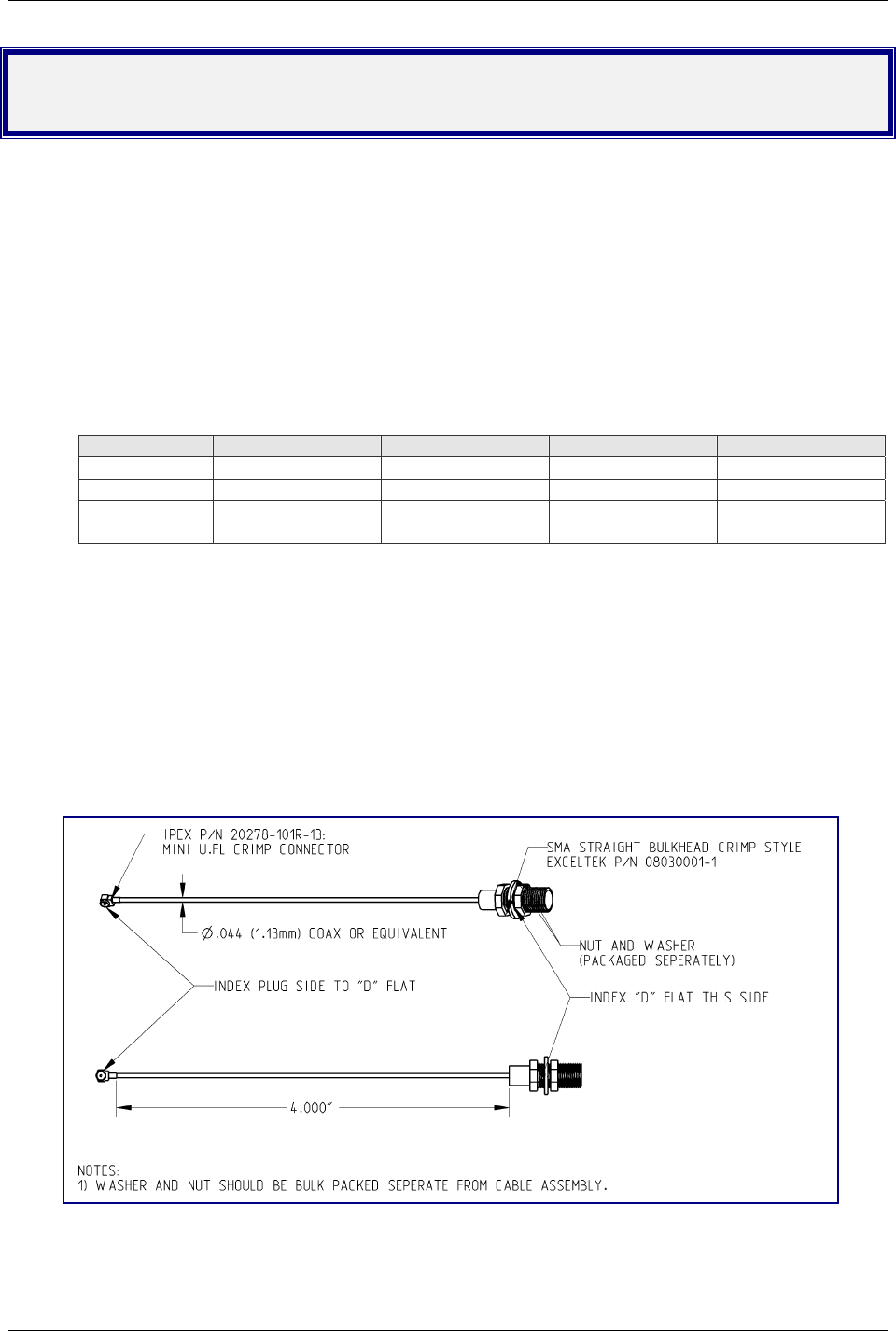
An optional 6” antenna cable (SMA Jack to UFL Plug) can be ordered from Multi-Tech Systems,
Inc.
Part Number Description
CASMA-UFL-1 SMA to UFL COAX RF 6 inch cable (Single Pack)
CASMA-UFL-10 SMA to UFL COAX RF 6 inch cable (Ten Pack)
Cable Specifications
Cable Type: Dia. 1.13mm Coaxial Cable
Attenuation: <1.0db
Connector Impedance: 50 ohm

Chapter 2 – The Antenna System
Multi-Tech Systems, Inc. SocketModem GSM Hardware Guide for Developers 13
Antenna
GSM Antenna Requirements/Specifications
Frequency Range: 824 – 960 MHz / 1710 – 1990 MHz
Impedance: 50 ohm
VSWR: <2.0:1
Typical Radiated Gain: 0 dBi on azimuth plane
Radiation: Omni
Polarization: Vertical
Wave: Half Wave Dipole
Antennas Available from Multi-Tech:
Quad Band Description Qty Part Number
Hinged Right Angle 800/900/1800/1900 MHz Cellular Modem Antenna 1 ANQB-1HRA
Hinged Right Angle 800/900/1800/1900 MHz Cellular Modem Antenna 10 ANQB-10HRA
Hinged Right Angle 800/900/1800/1900 MHz Cellular Modem Antenna 50 ANQB-50HRA
PTCRB Requirements Note:
There cannot be any alteration to the authorized antenna system. The antenna system must be
the same type with similar in-band and out-of-band radiation patterns and maintain the same
specifications.
FCC Requirements Note:
The antenna gain, including cable loss, must not exceed 3.1 dBi at 1900 MHz / 0.9 dBi at 850
MHz for mobile operating configurations and 7.1 dBi at 1900 MHz / 0.9 dBi at 850 MHz for fixed
mounted operations, as defined in 2.1091 and 1.1307 of the rules for satisfying RF exposure
compliance.

Chapter 3 – Design Considerations
Multi-Tech Systems, Inc. SocketModem GSM Hardware Guide for Developers 14
Chapter 3 – Design Considerations
Noise Suppression Design Considerations
Engineering noise-suppression practices must be adhered to when designing a printed circuit board
(PCB) containing the SocketModem module. Suppression of noise is essential to the proper operation
and performance of the modem itself and for surrounding equipment.
Two aspects of noise in an OEM board design containing the SocketModem must be considered: on-
board/off-board generated noise that can affect digital signal processing. Both on-board and off-board
generated noise that is coupled on-board can affect interface signal levels and quality. Of particular
concern is noise in frequency ranges affecting modem performance.
On-board generated electromagnetic interference (EMI) noise that can be radiated or conducted off-
board is a separate, but equally important, concern. This type of noise can affect the operation of
surrounding equipment. Most local government agencies have stringent certification requirements
that must be met for use in specific environments.
Proper PC board layout (component placement, signal routing, trace thickness and geometry, etc.)
component selection (composition, value, and tolerance), interface connections, and shielding are
required for the board design to achieve desired modem performance and to attain EMI certification.
Other aspects of proper noise-suppression engineering practices are beyond the scope of this
designer guide. The designer should consult noise suppression techniques described in technical
publications and journals, electronics and electrical engineering text books, and component supplier
application notes.
PC Board Layout Guidelines
In a 4-layer design, provide adequate ground plane covering the entire board. In 4-layer designs,
power and ground are typically on the inner layers. All power and ground traces should be 0.05
inches wide.
The recommended hole size for the SocketModem pins is 0.036 in. +/-0.003 in. in diameter. Spacers
can be used to hold the SocketModem vertically in place during the wave solder process. A spacer
should be placed on pin 32 and pin 64 of the SocketModem. A suggested part number for the spacer
is BIVAR 938-0.130 for P1 (0.310in) option SocketModems. The spacers can be left on permanently
and will not effect operation.
All creepages and clearances for the SocketModem have been designed to meet requirements of
safety standards EN60950 or EN60601. The requirements are based on a working voltage of 125V or
250V. When the recommended DAA* circuit interface is implemented in a third party design, all
creepage and clearance requirements must be strictly followed in order to meet safety standards. The
third party safety design must be evaluated by the appropriate national agency per the required
specification.
User accessible areas: Based on where the third party design is to be marketed, sold, or used, it may
be necessary to provide an insulating cover over all TNV exposed areas. Consult with the recognized
safety agency to determine the requirements.
Note: Even if the recommended design considerations are followed, there are no guarantees that a
particular system will comply with all the necessary regulatory requirements. It is imperative that
specific designs be completely evaluated by a qualified/recognized agency.
*DAA stands for Data Access Arrangement. DAA is the telephone line interface of the module.

Chapter 3 – Design Considerations
Multi-Tech Systems, Inc. SocketModem GSM Hardware Guide for Developers 15
Electromagnetic Interference (EMI)
Considerations
The following guidelines are offered specifically to help minimize EMI generation. Some of these
guidelines are the same as, or similar to, the general guidelines but are mentioned again to reinforce
their importance. In order to minimize the contribution of the SocketModem-based design to EMI, the
designer must understand the major sources of EMI and how to reduce them to acceptable levels.
1. Keep traces carrying high frequency signals as short as possible.
2. Provide a good ground plane or grid. In some cases, a multilayer board may be required with
full layers for ground and power distribution.
3. Decouple power from ground with decoupling capacitors as close to the SocketModem
module power pins as possible.
4. Eliminate ground loops, which are unexpected current return paths to the power source and
ground.
5. Decouple the telephone line cables at the telephone line jacks. Typically, use a combination
of series inductors, common mode chokes, and shunt capacitors. Methods to decouple
telephone lines are similar to decoupling power lines; however, telephone line decoupling
may be more difficult and deserves additional attention. A commonly used design aid is to
place footprints for these components and populate as necessary during performance/EMI
testing and certification.
6. Decouple the power cord at the power cord interface with decoupling capacitors. Methods to
decouple power lines are similar to decoupling telephone lines.
7. Locate high frequency circuits in a separate area to minimize capacitive coupling to other
circuits.
8. Locate cables and connectors so as to avoid coupling from high frequency circuits.
9. Lay out the highest frequency signal traces next to the ground grid.
10. If a multilayer board design is used, make no cuts in the ground or power planes and be sure
the ground plane covers all traces.
11. Minimize the number of through-hole connections on traces carrying high frequency signals.
12. Avoid right angle turns on high frequency traces. Forty-five degree corners are good;
however, radius turns are better.
13. On 2-layer boards with no ground grid, provide a shadow ground trace on the opposite side
of the board to traces carrying high frequency signals. This will be effective as a high
frequency ground return if it is three times the width of the signal traces.
14. Distribute high frequency signals continuously on a single trace rather than several traces
radiating from one point.
Electrostatic Discharge Control
All electronic devices should be handled with certain precautions to avoid damage due to the
accumulation of static charge.
See the ANSI/ESD Association Standard (ANSI/ESD S20.20-1999) – a document “for the
Development of an Electrostatic Discharge Control for Protection of Electrical and Electronic Parts,
Assemblies and Equipment.” This document covers ESD Control Program Administrative
Requirements, ESD Training, ESD Control Program Plan Technical Requirements
(grounding/bonding systems, personnel grooming, protected areas, packaging, marking, equipment,
and handling), and Sensitivity Testing.
Multi-Tech Systems, Inc. strives to follow all of these recommendations. Input protection circuitry has
been incorporated into the Multi-Tech devices to minimize the effect of this static buildup, proper
precautions should be taken to avoid exposure to electrostatic discharge during handling.
Multi-Tech uses and recommends that others use anti-static boxes that create a faraday cage
(packaging designed to exclude electromagnetic fields). Multi-Tech recommends that you use our
packaging when returning a product and when you ship your products to your customers.

Chapter 4 – Safety and Regulatory Compliance
Multi-Tech Systems, Inc. SocketModem GSM Hardware Guide for Developers 16
Chapter 4 – Safety and Regulatory
Compliance
Safety Notices and Warnings
Note to OEMs: The following safety statements may be used in the documentation of
your final product applications.
Telecom Safety Warning
1. Never install telephone wiring during a lightning storm.
2. Never install a telephone jack in wet locations unless the jack is specifically designed for wet
locations.
3. This product is to be used with UL and cUL listed computers.
4. Never touch uninsulated telephone wires or terminals unless the telephone line has been
disconnected at the network interface.
5. Use caution when installing or modifying telephone lines.
6. Avoid using a telephone during an electrical storm. There may be a remote risk of electrical
shock from lightning.
7. Do not use a telephone in the vicinity of a gas leak.
8. To reduce the risk of fire, use only 26 AWG or larger telecommunication line cord.
9. This product must be disconnected from its power source and telephone network interface
when servicing.
Wireless Safety
General Safety
The modem is designed for and intended to be used in fixed and mobile applications.
“Fixed” means that the device is physically secured at one location and is not able to be
easily moved to another location. “Mobile” means that the device is designed to be used
in other than fixed locations.
Caution: Maintain a separation distance of at least 20 cm (8 inches) is
normally maintained between the transmitter’s antenna and the body of
the user or nearby persons. The Modem is not designed for or intended
to be used in portable applications within 20 cm. (8 inches) of the body of
the user.
RF Interference Issues
It is important to follow any special regulations regarding the use of radio equipment due
in particular to the possibility of radio frequency, RF, interference. Please follow the
safety advice given below carefully.
• Switch OFF your wireless modem when in an aircraft. The use of cellular telephones in
an aircraft may endanger the operation of the aircraft, disrupt the cellular network and
is illegal. Failure to observe this instruction may lead to suspension or denial of cellular
telephone services to the offender, or legal action or both.
• Switch OFF your wireless modem when around gasoline or diesel-fuel pumps and
before filling your vehicle with fuel.
• Switch OFF your wireless modem in hospitals and any other place where medical
equipment may be in use.
• Respect restrictions on the use of radio equipment in fuel depots, chemical plants or
where blasting operations are in progress.

Chapter 4 – Safety and Regulatory Compliance
Multi-Tech Systems, Inc. SocketModem GSM Hardware Guide for Developers 17
• There may be a hazard associated with the operation of your wireless modem close to
inadequately protected personal medical devices such as hearing aids and
pacemakers. Consult the manufacturers of the medical device to determine if it is
adequately protected.
• Operation of your wireless modem close to other electronic equipment may also cause
interference if the equipment is inadequately protected. Observe any warning signs and
manufacturers’ recommendations.
Vehicle Safety
• Do not use your wireless modem while driving.
• Respect national regulations on the use of cellular telephones in vehicles. Road safety
always comes first.
• If incorrectly installed in a vehicle, the operation of wireless modem telephone could
interfere with the correct functioning of vehicle electronics. To avoid such problems, be
sure that qualified personnel have performed the installation. Verification of the
protection of vehicle electronics should be part of the installation.
• The use of an alert device to operate a vehicle’s lights or horn on public roads is not
permitted.
Maintenance of Your Modem
Your wireless modem is the product of advanced engineering, design, and craftsmanship
and should be treated with care. The suggestions below will help you to enjoy this
product for many years.
• Do not expose the wireless modem to any extreme environment where the temperature
is above 50ºC or humidity is above 90% noncondensing.
• Do not attempt to disassemble the wireless modem. There are no user serviceable
parts inside.
• Do not expose the wireless modem to water, rain, or spilled beverages. It is not
waterproof.
• Do not place the wireless modem alongside computer discs, credit or travel cards, or
other magnetic media. The phone may affect the information contained on discs or
cards.
• The use of accessories not authorized by Multi-Tech or not compliant with Multi-Tech's
accessory specifications may invalidate the warranty of the wireless modem.
• In the unlikely event of a fault in the wireless modem, contact Multi-Tech Tech Support.
Your Responsibility
This wireless modem is your responsibility. Please treat it with care respecting all local
regulations. It is not a toy. Therefore, keep it in a safe place at all times and out of the
reach of children.
Try to remember your Unlock and PIN codes. Become familiar with and use the security
features to block unauthorized use and theft.
Chapter 4 – Safety and Regulatory Compliance
Multi-Tech Systems, Inc. SocketModem GSM Hardware Guide for Developers 18
Certifications, Approvals, Compliance, and
Requirements
Wireless Approvals
The Multi-Tech SocketModem is Industry and/or Carrier Approved as an End Product modem. When
integrated and used with an antenna system that was part of the Multi-Tech modem certification, no
additional approvals or certification are required (however, CDMA has a few exceptions) for the
device you develop as long as the following are met:
• PTCRB Requirements:
The antenna system cannot be altered.
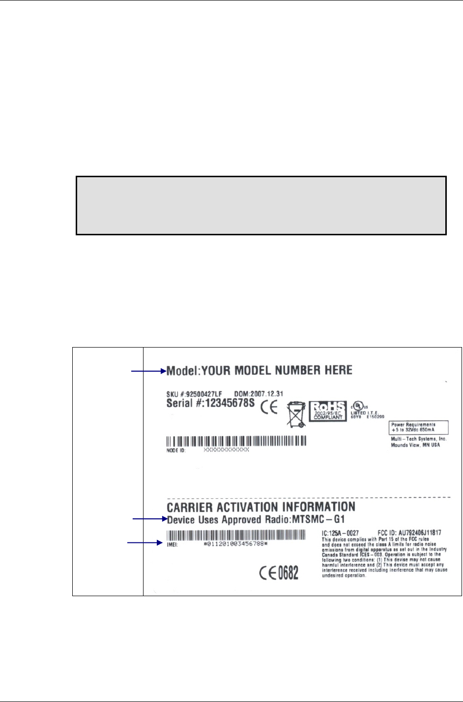
• Model Identification:
IMPORTANT
When the wireless carrier asks you to provide the modem's model identification,
give the Multi-Tech wireless model identification, not the identification of the host
device.
See the label example below.
The Multi-Tech model identification allows the carrier to verify the modem as one of its
approved models.
This information is located on the modem's label.
Example:
The following is an example of Multi-Tech's wireless model identification:
MTSMC-G1 – Multi-Tech wireless GSM model identification.
The following is an example of what an end product label could look like. End
product includes an integrated GSM modem:
Host Device
Identification
Multi-Tech
Model
Identification
IMEI
(International
Mobile
Equipment
Identity)
• Other Information the Wireless Carrier Asks You to Provide:
The modem's 15-character IMEI (International Mobile Equipment Identity) number printed
on the modem's label.

Chapter 4 – Safety and Regulatory Compliance
Multi-Tech Systems, Inc. SocketModem GSM Hardware Guide for Developers 19
Regulatory Compliance Statements
EMC, Safety, and R&TTE Directive Compliance
The CE mark is affixed to this product to confirm compliance with the following European Community
Directives:
Council Directive 89/336/EEC of 3 May 1989 on the approximation of the laws of Member States
relating to electromagnetic compatibility;
and
Council Directive 73/23/EEC of 19 February 1973 on the harmonization of the laws of Member
States relating to electrical equipment designed for use within certain voltage limits;
and
Council Directive 1999/5/EC of 9 March on radio equipment and telecommunications terminal
equipment and the mutual recognition of their conformity.
International Modem Restrictions
Some dialing and answering defaults and restrictions may vary for international modems. Changing
settings may cause a modem to become non-compliant with national telecom requirements in specific
countries. Also note that some software packages may have features or lack restrictions that may cause
the modem to become non-compliant.
EMC Requirements for the United States
FCC Part 15 Regulation
This equipment has been tested and found to comply with the limits for a Class B digital device,
pursuant to Part 15 of the FCC rules. These limits are designed to provide reasonable protection
against harmful interference in a residential installation. This equipment generates, uses, and can
radiate radio frequency energy, and if not installed and used in accordance with the instructions, may
cause harmful interference to radio communications. However, there is no guarantee that interference
will not occur in a particular installation. If this equipment does cause harmful interference to radio or
television reception, which can be determined by turning the equipment off and on, the user is
encouraged to try to correct the interference by one or more of the following measures:
Reorient or relocate the receiving antenna.
Increase the separation between the equipment and receiver.
Plug the equipment into an outlet on a circuit that is different from the one used by the receiver.
Consult the dealer or an experienced radio/TV technician for help.
This device complies with Part 15 of the FCC rules. Operation of this device is subject to the following
conditions: (1) This device may not cause harmful interference, and (2) this device must accept any
interference that may cause undesired operation.
WARNING – Changes or modifications to this unit not expressly approved by the party responsible for
compliance could void the user’s authority to operate the equipment.
EMC Requirements for Industry Canada
This Class B digital apparatus meets all requirements of the Canadian Interference-Causing Equipment
Regulations.
Cet appareil numérique de la classe B respecte toutes les exigences du Reglement Canadien sur le
matériel brouilleur.
Chapter 4 – Safety and Regulatory Compliance
Multi-Tech Systems, Inc. SocketModem GSM Hardware Guide for Developers 20
Waste Electrical and Electronic Equipment
Statement
Note to OEMs: The statement is included for your information and may be used in
the documentation of your final product applications.
WEEE Directive
The WEEE directive places an obligation on EU-based manufacturers, distributors, retailers, and importers
to take-back electronics products at the end of their useful life. A sister Directive, ROHS (Restriction of
Hazardous Substances) complements the WEEE Directive by banning the presence of specific hazardous
substances in the products at the design phase. The WEEE Directive covers all Multi-Tech products
imported into the EU as of August 13, 2005. EU-based manufacturers, distributors, retailers and importers
are obliged to finance the costs of recovery from municipal collection points, reuse, and recycling of
specified percentages per the WEEE requirements.
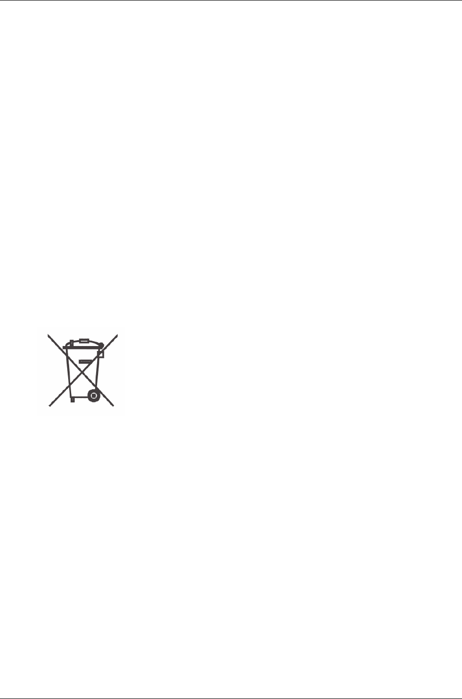
Instructions for Disposal of WEEE by Users in the European Union
The symbol shown below is on the product or on its packaging, which indicates that this product must not be
disposed of with other waste. Instead, it is the user’s responsibility to dispose of their waste equipment by
handing it over to a designated collection point for the recycling of waste electrical and electronic equipment.
The separate collection and recycling of your waste equipment at the time of disposal will help to conserve
natural resources and ensure that it is recycled in a manner that protects human health and the
environment. For more information about where you can drop off your waste equipment for recycling, please
contact your local city office, your household waste disposal service or where you purchased the product.
July, 2005

Chapter 4 – Safety and Regulatory Compliance
Multi-Tech Systems, Inc. SocketModem GSM Hardware Guide for Developers 21
Restriction of the Use of Hazardous Substances
(RoHS)
Multi-Tech Systems, Inc.
Certificate of Compliance
2002/95/EC
Multi-Tech Systems Inc. confirms that its embedded products now comply with the chemical concentration
limitations set forth in the directive 2002/95/EC of the European Parliament (Restriction Of the use of certain
Hazardous Substances in electrical and electronic equipment - RoHS)
These Multi-Tech Systems, Inc. products do not contain the following banned chemicals:
Lead, [Pb] < 1000 PPM
Mercury, [Hg] < 1000 PPM
Hexavalent Chromium, [Cr+6] < 1000 PPM
Cadmium, [Cd] < 100 PPM
Polybrominated Biphenyl, [PBB] < 1000 PPM
Polybrominated Diphenyl Ether, [PBDE] < 1000 PPM
Moisture Sensitivity Level (MSL) =1
Tin Whisker Growth = None detected
Maximum Soldering temperature = 260C (wave only)
Notes:
1. Lead usage in some components is exempted by the following RoHS annex; therefore, higher lead
concentration would be found in some modules (>1000ppm).
a. Lead in high melting temperature type solders (i.e., tin-lead solder alloys containing more
than 85% lead).
b. Lead in electronic ceramic parts (e.g., piezoelectronic devices).
2. Moisture Sensitivity Level (MSL) – Analysis is based on the components/material used on the
board.
3. Tin Whisker Study was done per NEMI guidelines (Elevated temperature cycle of 60°C and non-
condensing relative humidity of 87% exposed to this environment for 1000 hours).
Chapter 4 – Safety and Regulatory Compliance
Multi-Tech Systems, Inc. SocketModem GSM Hardware Guide for Developers 22
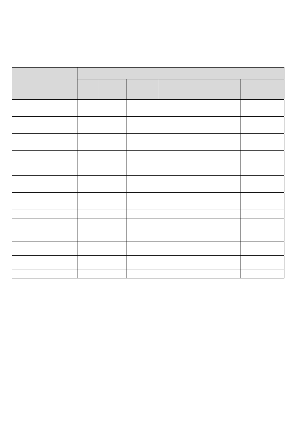
Information on HS/TS Substances According to
Chinese Standards
In accordance with China’s Administrative Measures on the Control of Pollution Caused by Electronic Information
Products (EIP) # 39, also known as China RoHS, the following information is provided regarding the names and
concentration levels of Toxic Substances (TS) or Hazardous Substances (HS) which may be contained in Multi-
Tech Systems Inc. products relative to the EIP standards set by China’s Ministry of Information Industry (MII).
Hazardous/Toxic Substance/Elements
Name of the
Component Lead
(PB) Mercury
(Hg) Cadmium
(CD) Hexavalent
Chromium
(CR6+)
Polybrominated
Biphenyl (PBB) Polybrominated
Diphenyl Ether
(PBDE)
Printed Circuit Boards O O O O O O
Resistors X O O O O O
Capacitors X O O O O O
Ferrite Beads O O O O O O
Relays/Opticals O O O O+ O O
ICs O O O O O O
Diodes/ Transistors O O O O O O
Oscillators and Crystals X O O O O O
Regulator O O O O O O
Voltage Sensor O O O O O O
Transformer O O O O O O
Speaker O O O O O O
Connectors O O O O O O
LEDs O O O O O O
Screws, Nuts, and other
Hardware X O O O O O
AC-DC Power Supplies O O O O O O
Software /
Documentation CDs O O O O O O
Booklets and
Paperwork O O O O O O
Chassis O O O O O O
X Represents that the concentration of such hazardous/toxic substance in all the units of homogeneous
material of such component is higher than the SJ/Txxx-2006 Requirements for Concentration Limits.
O Represents that no such substances are used or that the concentration is within the aforementioned limits.
Chapter 4 – Safety and Regulatory Compliance
Multi-Tech Systems, Inc. SocketModem GSM Hardware Guide for Developers 23
Information on HS/TS Substances According to
Chinese Standards (in Chinese)
依照中国标准的有毒有害物质信息
根据中华人民共和国信息产业部 (MII) 制定的电子信息产品 (EIP)
标准-中华人民共和国《电子信息产品污染控制管理办法》(第 39 号),也称作中国
RoHS,下表列出了 Multi-Tech Systems, Inc. 产品中可能含有的有毒物质 (TS) 或有害物质
(HS) 的名称及含量水平方面的信息。
有害/有毒物质/元素
成分名称 铅
(PB)
汞
(Hg)
镉
(CD)
六价铬
(CR6+)
多溴联苯
(PBB)
多溴二苯醚
(PBDE)
印刷电路板 O O O O O O
电阻器 X O O O O O
电容器 X O O O O O
铁氧体磁环 O O O O O O
继电器/光学部件 O O O O O O
IC O O O O O O
二极管/晶体管 O O O O O O
振荡器和晶振 X O O O O O
调节器 O O O O O O
电压传感器 O O O O O O
变压器 O O O O O O
扬声器 O O O O O O
连接器 O O O O O O
LED O O O O O O
螺丝、螺母以及其
它五金件
X O O O O O
交流-直流电源 O O O O O O
软件/文档 CD O O O O O O
手册和纸页 O O O O O O
底盘 O O O O O O
X 表示所有使用类似材料的设备中有害/有毒物质的含量水平高于 SJ/Txxx-2006 限量要求。
O 表示不含该物质或者该物质的含量水平在上述限量要求之内。
Chapter 5 – The SocketModem Developer Board
Multi-Tech Systems, Inc. SocketModem GSM Hardware Guide for Developers 24
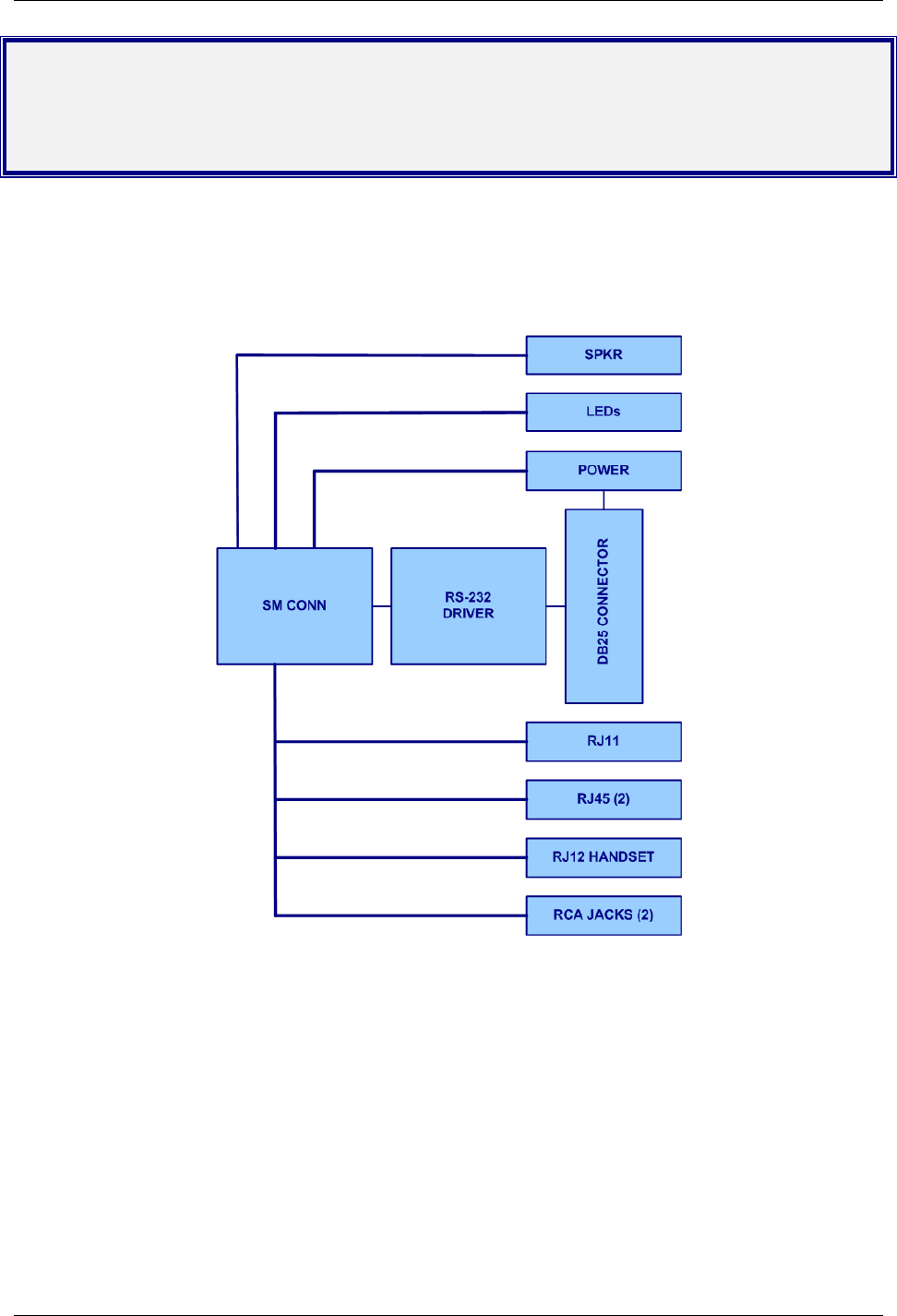
Chapter 5 – The SocketModem
Developer Board
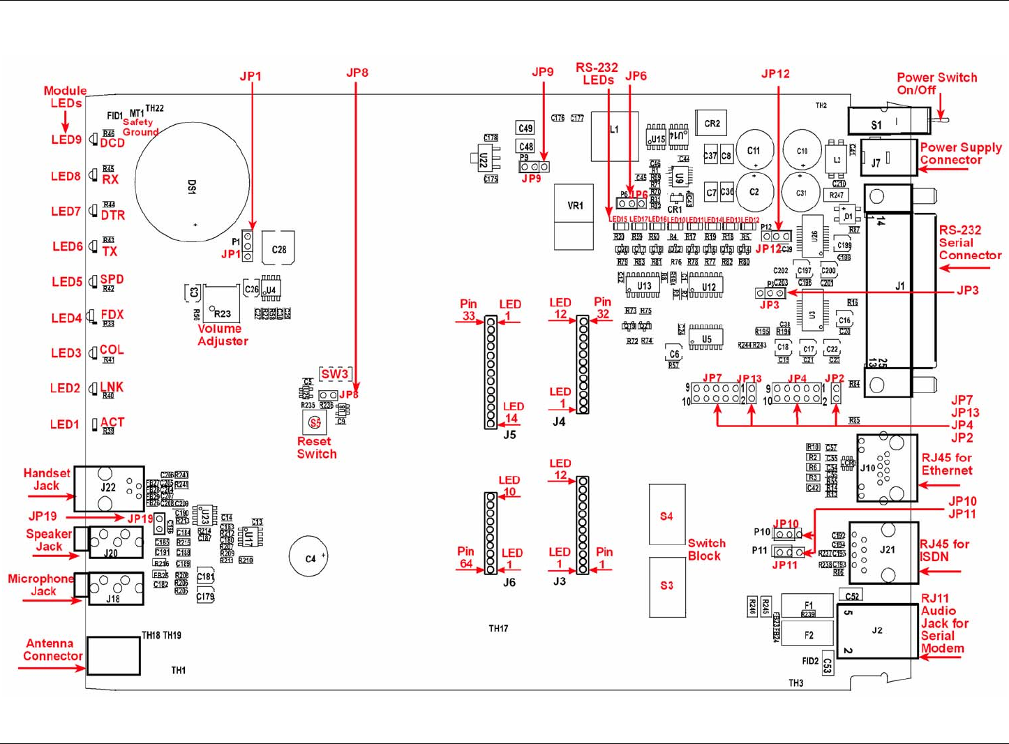
SocketModem Developer Board Block Diagram
Chapter 5 – The SocketModem Developer Board
Multi-Tech Systems, Inc. SocketModem GSM Hardware Guide for Developers 25
The Developer Board Components
See the next page for a description of the Board Components.
Chapter 5 – The SocketModem Developer Board
Multi-Tech Systems, Inc. SocketModem GSM Hardware Guide for Developers 26
Board Components
Jumper Description
JP1 Mutes the speaker. Default positions are 1 and 2 (speaker is not muted).
JP2 & 4 Testing interface (debugging) for the RS-232 signals.
JP3 Changes the speed of the driver. For Multi-Tech use only. Default positions are 1
and 2 (transceiver operates normally).
JP6 & JP9 JP6 & JP9 are the 5V / 3.3V regulators. The operating voltage factory default
setting is 3.3V.
JP1 jumper must be set to 3.3V.
Warning – Be sure to that 5V / 3.3V jumper is set to match the requirements of
your SocketModem. If this jumper is set incorrectly, damage to the
SocketModem and/or the Test/Demo card could result.
Caution – Use only the provided Multi-Tech Systems, Inc. transformer with the
Test/Demo board. Use of any other power source will void the warranty and will
likely damage the Test/Demo board and the SocketModem. The transformer
connector is keyed to prevent improper connection to the Test/Demo board.
JP7 & JP13 Testing interface (debugging) for the serial TTL signals.
JP8 Enables/disables the Watchdog interface.
JP10 & JP11 100 OHM terminator for ISDN. Default positions are 1 and 2 (off).
JP12 Ties the TX and RX clock lines together. Default positions are 1 and 2 (transmit
and receiver clock act independently.
JP19 Allows a stereo jack feed. Default is ON. If ON, then left and right stereo
channels are combined and form a mono channel.
Switch 3 Sets the alternate ISDN clock. Default position is OFF (the alternate ISDN clock
is off).
Switch Block Set the switch to the product being used.
Pins and Corresponding Signals
J4 and J7
10 PWR
8 CTS
6 DSR
4 DTR
2 RXD
9 RI
7 RTS
5 GND
3 TXD
1 DCD
J2 and J13
2 RXC 1 TXC
Chapter 5 – The SocketModem Developer Board
Multi-Tech Systems, Inc. SocketModem GSM Hardware Guide for Developers 27
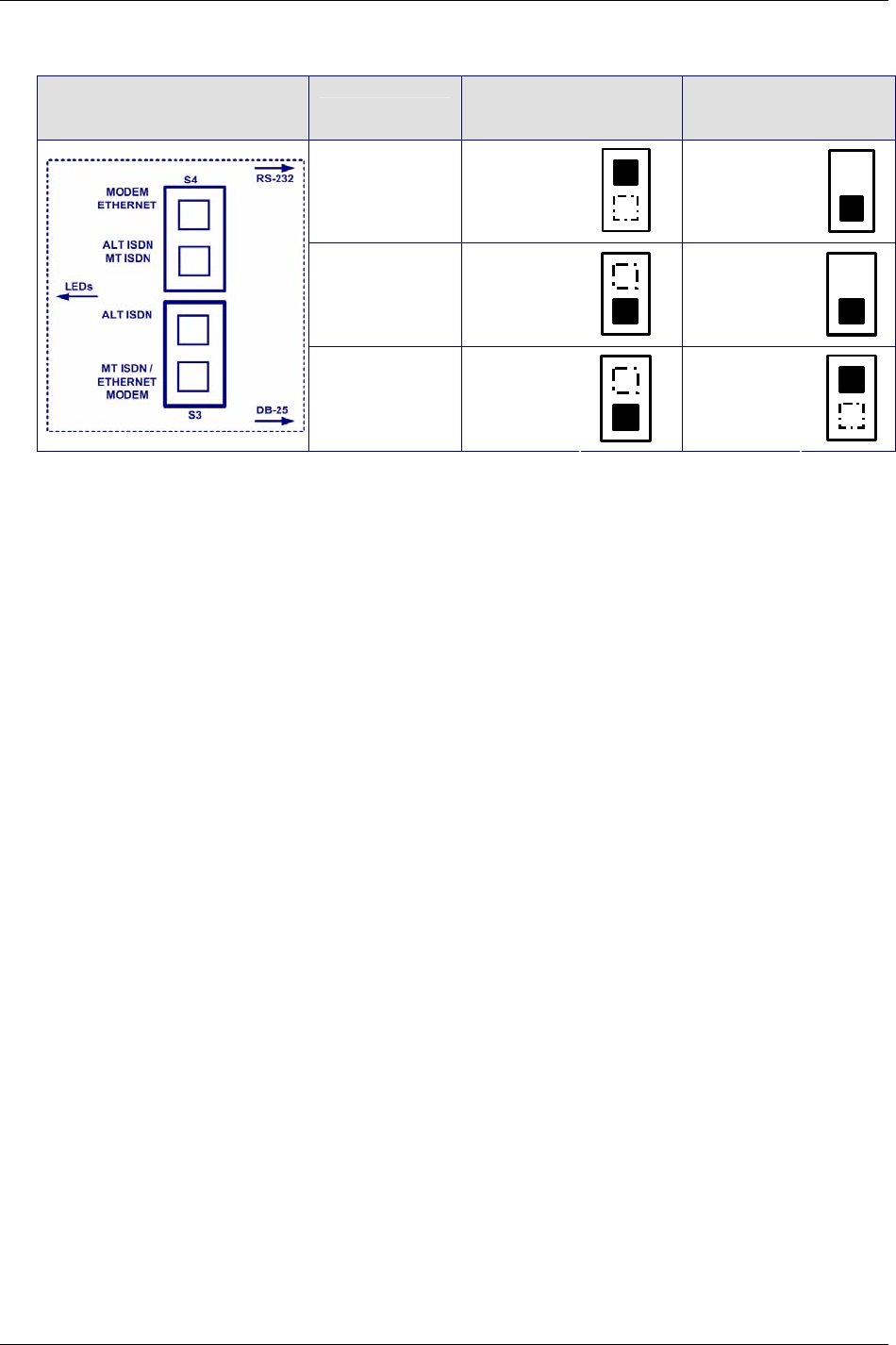
Table of Switch Blocks
Switch Blocks and Board
Orientation
Module Style Board Labels & Block
Settings – S4 Board Labels & Block
Settings – S3
Non-ISDN
SocketModems
and
SocketEthernet IP
“MODEM
ETHERNET”
“MT ISDN /
ETHERNET
MODEM”
Standard ISDN
“ALT ISDN
MT ISDN”
“MT ISDN /
ETHERNET
MODEM”
Alternate ISDN
“ALT ISDN
MT ISDN”
“ALT ISDN”
Note: ALT stands for alternate ISDN
Chapter 5 – The SocketModem Developer Board
Multi-Tech Systems, Inc. SocketModem GSM Hardware Guide for Developers 28
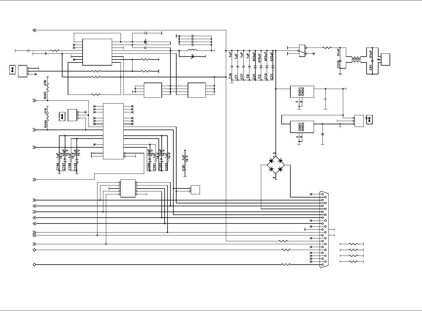
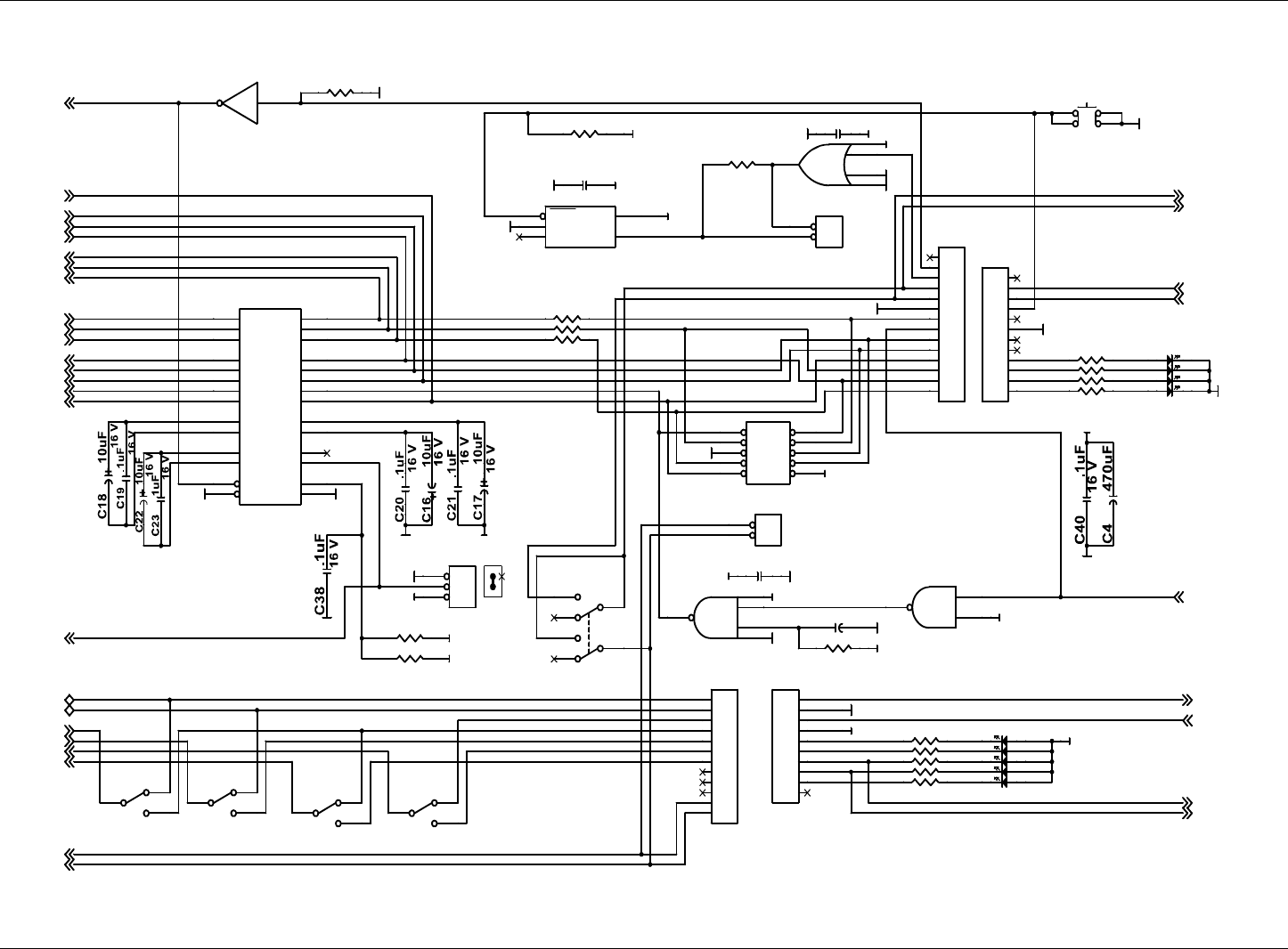
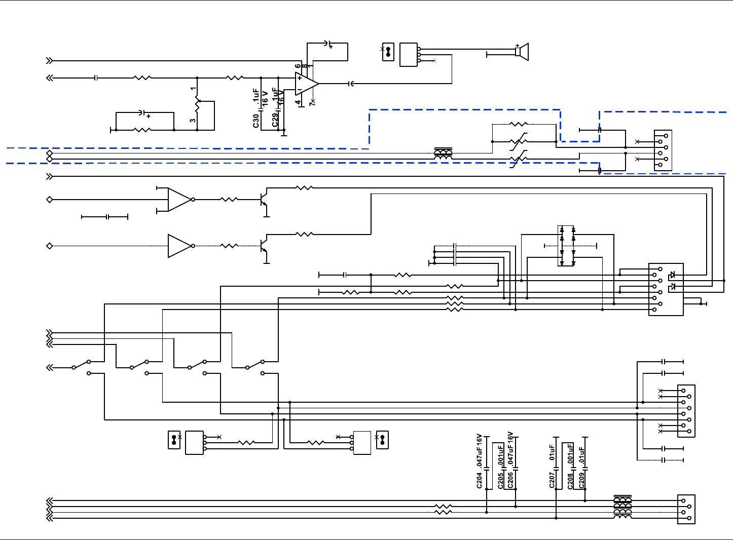
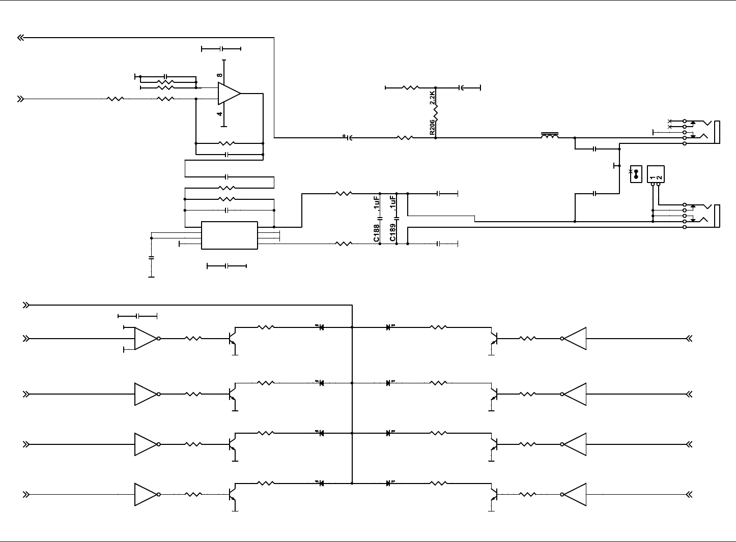
Developer Board Schematics
SHUNT ON:
1&2=TDCLK
2&3=SYNC
VIN
VIN4,5
DSR3
TXD3
DTR3
RXD3
RI3
RTS3
CTS3
DCD3
RXCLK3
MBAUD3
SLP3
TIP3,4
RING3,4
TXCLK3
GND
GND
GND
GND
GND
GND
GND
CGND
CGND
CGND
CGND
CGND
CGND
GND
GND
GND GND
GND
GND
GND
GND
GND
GND
GND
GND
GND
GND
VCC5
GND
GND GND
GND GND
GND
GND
GND
VDD3_3
VCC
VCC
VCC
VCC
VCC
VCC
VCC
VCC
VCC
U14
Si4840DY
6
8
2
37
4
1
5
D2
D4
S2
S3 D3
G1
S1
D1
R247 1
CR1 MMBD301LT1
R32 24.3K
U9
LTC1778
8
5
7
6
1
2
4
3
9
10
11
12
13
14
15
16
VFB
ITH
ION
SGND
RUN/SS
PGOOD
FCB
VRNG
EXTVCC
VIN
INTVCC
BG
PGND
SW
TG
BOOST
JP4
HEADER-5x2
12
34
56
78
910
U22 TC1262
13
VIN VOUT
C178
1uF
16 V
R246 0
R85 0
C177 .1uF 16 V
JP12
HEADER-3
1
2
3
P9
SHUNT
R69 22K
P12
SHUNT
C45 470pF L1 15uH
R1 100K R31 15.8K
+
R86 0
CR2 40V/3A
+
J7
ZDX-POWER-CON
1
2
3
R70 49.9K
C176 .01uF
C175
1uF
16 V
S1
SW-SPDT
23
15
4
JP9
HEADER-3
1
2
3
VR1 LD29300
1 3
VIN VOUT
+
C43 10uF
10 V
J1
25-POS/D-SUB
13
25
12
24
11
23
10
22
9
21
8
20
7
19
6
18
5
17
4
16
3
15
2
14
1
26
27
R87 0
C48 100uF 6.3 V
L2
ZJYS-2
1
2 3
4
C46 .1uF
16 V
+
C49 100uF 6.3 V
U15
Si4840DY
6
8
2
37
4
1
5
D2
D4
S2
S3 D3
G1
S1
D1
JP2
HEADER-2
1
2
D1
MB4S
1 2
+
R71 2.2M
C44 .22uF 16 V
R16 330
R245 0
JP6
HEADER-3
1
2
3
U26
ICL3237E
21 8
20
18
24
23
22
19
17
27
4
26
2
9
11
5
6
7
10
12
28
25
1
3
13
14
15
16
R10UT R1IN
R2OUT
R3OUT
T1IN
T2IN
T3IN
T4IN
T5IN
V+
V-
VCC
GND
R2IN
R3IN
T1OUT
T2OUT
T3OUT
T4OUT
T5OUT
C1+
C1-
C2+
C2-
EN
SHDN
MBAUD
R1OUTB
R84 0
P6
SHUNT
Chapter 5 – The SocketModem Developer Board
Multi-Tech Systems, Inc. SocketModem GSM Hardware Guide for Developers 29
Developer Board Schematics
Place close to
the Module.
RESET
TXIND
DTRTTL
RTSTTL
RXIND
DCIND
DTRIND
TXDTTL
ACT
SPD
COL
LINK
FDX
RING
TIP
RXDTTL
DSRTTL
CTSTTL
RITTL
DSRTTL
RITTL
CTSTTL
RXDTTL
DTR2TXD2RTS2
RXD2CTS2DSR2DCD2RI2
DTRTTL5
RTSTTL5TXDTTL5
CTSTTL5RXDTTL
5
DSRTTL5
RITTL5
ACT 4
RX+4
TX-4RX-
4
SPKR 4,5TIP2,4
TX+
4
RING2,4
LINK 4
DCDTTL 5
MIC 5
SPK_P 4
SPK_N 4
MIC_N 4
MIC_P 4
RXCLK
2
MBAUD2
SLP2
TXCLK2
GND
GND
GND
GND
GND
GND
GND
VCC5
GND
GND
GND
GND
GND
GND
GND
GND
GND
GND
GND
GND
GND
GND
VCC
VCC
VCC VCC
VCC
VCC
VCC
VCC
VCC
VCC
VCC
VCC
VCC
VCC
VCC
VCC
+
C6 10uF
16 V
J3
12-PIN-SOC
1
2
3
4
5
6
7
8
9
10
11
12
S3-1
SW-4PDT
23
1
R44 150
JP7
HEADER-5x2
1 2
3 4
5 6
7 8
R41 200
R39 200
+
U25
ADM6318
1
4
3
5
2RESET
WDIRESET
VCC
GND
S3-2
SW-4PDT
11 10
12
R57 10K
S5
SW-SPST
13
2 4
R45 150
SW3
SW-DPDT
2
1
3
5
4
6
R194 47K
C24 .01uF
R7 0
LED5 RED
U3
ICL3237E
21
820
18
24
23
22
19
17
27
4
26
2
9
11
5
6
7
10
12
28
25
1
3
13
14
15
16
R10UTR1IN R2OUT
R3OUT
T1IN
T2IN
T3IN
T4IN
T5IN
V+
V-
VCC
GND
R2IN
R3IN
T1OUT
T2OUT
T3OUT
T4OUT
T5OUT
C1+
C1-
C2+
C2-
EN
SHDN
MBAUD
R1OUTB
LED3 RED
C5 .01uF
LED1 RED
U12F
74LCX04
12 13
LED9 RED
R236 0
S3-3
SW-4PDT
87
9
J4
12-PIN-SOC
1
2
3
4
5
6
7
8
9
10
11
12 LED6 RED
R46 150
R195 0
U5B
74VHC00
4
5
6
R8 0
J6
10-PIN-SOC
1
2
3
4
5
6
7
8
9
10
JP3
HEADER-3
1
2
3
C9 .01uF
R40 200
U5A
74VHC00
1
2
3
14
7
JP13
HEADER-2
1
2
U8
7S32
1
2
45
3
R38 200
J5
14-PIN-SOC
1
2
3
4
5
6
7
8
9
10
11
12
13
14
R196 0
R43 150
S3-4
SW-4PDT
56
4
LED8 RED
R9 0
JP8
HEADER-2
1
2
P3
SHUNT
R235 4.7K
LED2 RED
LED7 RED
LED4 RED
R42 200
9 10
Chapter 5 – The SocketModem Developer Board
Multi-Tech Systems, Inc. SocketModem GSM Hardware Guide for Developers 30
Developer Board Schematics
TX TERM.
SHUNT ON:
1&2=OPEN
2&3=100
OHM
SHUNT ON:
1&2=OPEN
2&3=100
OHM
HANDSET
RX TERM.
I_RX-
I_RX+
E_TX-
E_TX+
E_RX-
E_RX+
I_TX+
I_TX-
RING2,3 TIP2,3
SPKR3,5
ACT
3
LINK
3
VIN2,5
VIN2,5
SPK_N3SPK_P3MIC_N3
MIC_P3
TX+3RX-3RX+3
TX-3
GND
GND
GND
GND
GND
GND
GND
GND
GND
GND
GND
GND
CGND
CGND
CGND
CGND
CGND
CGND
CGND
VCC
VCC
VCC
GND
GND
GND
GND
R75 47K
C192 .01uF
JP10
HEADER-3
1
2
3
R55 0
S4-3
SW-4PDT
87
9
C26 10uF
16 V
C54 15pF
R241 9.09
U4
LM386
2
35
FB27
C53 220pF
5KV
R73 47K
J2
6X4-MODJACK
5
4
3
2
R22 4.7K
R23
10K 2
R13 75
J21
8X8-MODJACK
5
4
3
2
6
1
7
8
C55 15pF
C194 .01uF
S4-4
SW-4PDT
56
4
R239 0
Q21
2N3904
JP1
HEADER-3
1
2
3
CR3
DALC208SC6
5
3
16
2
4
FB28
BLM18AG102SN1
R56 1K
R74 2.7K
U13B
74LCX04
3 4
R58 4.7K
J22
4X4-MODJACK
1
2
3
4
R14 75
C56 15pF
DS1
SPEAKER
1
2
R237 100
S4-1
SW-4PDT
23
1
FB29
C3 10uF
16 V
C195 .01uF
FB23 600-OHM
P1
SHUNT
C57 15pF
R238 100
C193 .01uF
C27 .1uF
16 V
P11
SHUNT
JP11
HEADER-3
1
2
3
C42 .001uF
2KV
S4-2
SW-4PDT
11 10
12
Q19
2N3904
F1 145mA
FB24 600-OHM
C52 220pF
5KV
R240 9.09
U13A
74LCX04
14
7
1 2
FB26
C12 .01uF
R72 2.7K
+
C28 100uF
16 V
J10
8X8-MODJACK-2LEDS
5
4
3
2
6
1
7
89
10
11
12
13
14
F2 145mA
P10
SHUNT
R6 0
R3 0
R2 0
R10 0
Safety Isolation Barrier
NOTE:
C192, C193, C194, C195
are not installed on
the board by default.
Chapter 5 – The SocketModem Developer Board
Multi-Tech Systems, Inc. SocketModem GSM Hardware Guide for Developers 31
Developer Board Schematics
DCDTTL 3
DTRTTL
3
RXDTTL 3
DSRTTL
3
CTSTTL
3TXDTTL 3
RTSTTL
3RITTL 3
VIN
2,4
MIC
3
SPKR
3,4
GND
GND
GND
GND
GND
GND
GND
GND
GND
GND
GND
GND
GND
GND
GND
GND
GND
GND
GND
GND
GND
GND
VCC
VCC
VCC
VCC
VCC
VCC
VCC
VCC
R78 47K
U13C
74LCX04
5
6
C187 4.7pF
Q14
2N3904
C191 .01uF
R80 47K
R214 2.7K
FB25
MLB20
R205 10K
C13 .01uF
R77 47K
R207 47K
C186 .001uF
100 V
R82 47K
R209 47K
+
C179 10uF
16V
C180 .01uF
Q18
2N3904
R211 10K
C183 .001uF
C14 .01uF
R210 0
R18 2.7K
C181 1uF
U12C
74LCX04
5 6
R212 47K
U12A
74LCX04
14
7
1 2
C182 .001uF
100 V
R81 47K
+
-
U17A
V+
V-
TL082
1
3
2
Q17
2N3904
U12E
74LCX04
10 11
R213 10K
U23
LM4861
1
2
4
35
8
6
7
SHUTDOWN
BYPASS
IN-
IN+ VO1
VO2
VDD
GND
Q20
2N3904
U12B
74LCX04
3 4
U13D
74LCX04
8 9
R216 0
Q15
2N3904
Q13
2N3904
P19
SHUNT
U12D
74LCX04
89
R76 47K
C1 .01uF
C185 .01uF
U13E
74LCX04
10 11
J19
HEADER-2
R79 47K
LED13 RED
J20
5-PIN-STEREO-JACK
4
3
5
2
1
Q12
2N3904
C184 .47uF
25 V
R208 301K
J18
5-PIN-STEREO-JACK
4
3
5
2
1
Q16
2N3904
16 V
C190
.1uF
R5 2.7K LED12 RED
R17 2.7K LED11 RED
R4 2.7K LED10 RED
R215 0
LED17 RED R59 2.7K
LED16 RED R60 2.7K
LED15 RED R20 2.7K
LED14 RED R19 2.7K
R83 47K

Chapter 6 – The Multi-Tech Warranty Statement
Multi-Tech Systems, Inc. SocketModem GSM Hardware Guide for Developers 32
Chapter 6 – Multi-Tech Warranty
Statement
The Multi-Tech Systems, Inc. Warranty Policy
Multi-Tech Systems, Inc., (hereafter “MTS”) warrants that its products will be free from defects in material or
workmanship for a period of two, five, or ten years (depending on model) from date of purchase, or if proof of
purchase is not provided, two, five, or ten years (depending on model) from date of shipment.
MTS MAKES NO OTHER WARRANTY, EXPRESS OR IMPLIED, AND ALL IMPLIED WARRANTIES OF
MERCHANTABILITY AND FITNESS FOR A PARTICULAR PURPOSE ARE HEREBY DISCLAIMED.
This warranty does not apply to any products which have been damaged by lightning storms, water, or power surges
or which have been neglected, altered, abused, used for a purpose other than the one for which they were
manufactured, repaired by Customer or any party without MTS’s written authorization, or used in any manner
inconsistent with MTS’s instructions.
MTS’s entire obligation under this warranty shall be limited (at MTS’s option) to repair or replacement of any products
which prove to be defective within the warranty period or, at MTS’s option, issuance of a refund of the purchase price.
Defective products must be returned by Customer to MTS’s factory — transportation prepaid.
MTS WILL NOT BE LIABLE FOR CONSEQUENTIAL DAMAGES, AND UNDER NO CIRCUMSTANCES WILL ITS
LIABILITY EXCEED THE PRICE FOR DEFECTIVE PRODUCTS.
Repair Procedures for U.S. and Canadian Customers
In the event that service is required, products may be shipped, freight prepaid, to our Mounds View,
Minnesota factory:
Multi-Tech Systems, Inc.
2205 Woodale Drive
Mounds View, MN 55112 U.S.A.
Attn: Repairs, Serial # ____________
A Returned Materials Authorization (RMA) is not required. Return shipping charges (surface) will be paid by
MTS to destinations in U.S. and Canada.
Please include, inside the shipping box, a description of the problem, a return shipping address (must have
street address, not P.O. Box), your telephone number, and if the product is out of warranty, a payment in
advance is required. Acceptable means of payment include credit card, wire transfer or a check in U.S.
dollars drawn on a U.S. Bank.
For out of warranty repair charges, go to COMPANY/Policies/warranty/
Extended two-year overnight replacement service agreements are available for selected products. Please
call MTS customer service at (888) 288-5470 or visit our web site at
/PARTNERS/Programs/overnight_replacement/ for details on rates and coverages.
Please direct your questions regarding technical matters, product configuration, verification that the product
is defective, etc., to our Technical Support department at (800) 972-2439 or email support@multitech.com.
Please direct your questions regarding repair expediting, receiving, shipping, billing, etc., to our Repair
Accounting department at (800) 328-9717 or (763) 717-5631, or email mtsrepair@multitech.com.
Repairs for damages caused by lightning storms, water, power surges, incorrect installation, physical abuse,
or user-caused damages are billed on a time-plus-materials basis.
Repair Procedures for International Customers
(Outside U.S.A. and Canada)
Your original point-of-purchase Reseller may offer the quickest and most economical repair option for your
Multi-Tech product. You may also contact any Multi-Tech sales office for information about the nearest
distributor or other repair service for your Multi-Tech product. The Multi-Tech sales office directory is
available at www.multitech.com/PARTNERS/Channels/offices/
In the event that factory service is required, products may be shipped, freight prepaid to our Mounds View,
Minnesota factory. Recommended international shipment methods are via Federal Express, UPS or DHL
courier services, or by airmail parcel post; shipments made by any other method will be refused. Please
include, inside the shipping box, a description of the problem, a return shipping address (must have street
address, not P.O. Box), your telephone number, and if the product is out of warranty, a payment in advance
is required. Acceptable means of payment include credit card, wire transfer or a check in U.S. dollars drawn

Chapter 6 – The Multi-Tech Warranty Statement
Multi-Tech Systems, Inc. SocketModem GSM Hardware Guide for Developers 33
on a U.S. Bank. Repaired units shall be shipped freight collect, unless other arrangements are made in
advance.
Please direct your questions regarding technical matters, product configuration, verification that the product
is defective, etc., to our Technical Support department nearest you or email support@multitech.com. When
calling the U.S., please direct your questions regarding repair expediting, receiving, shipping, billing, etc., to
our Repair Accounting department at +(763) 717-5631 in the U.S.A., or email mtsrepair@multitech.com.
Repairs for damages caused by lightning storms, water, power surges, incorrect installation, physical abuse,
or user-caused damages are billed on a time-plus-materials basis.
Repair Procedures for International Distributors
International distributors should contact their MTS International sales representative for information about
the repair of Multi-Tech product(s).
Please direct your questions regarding technical matters, product configuration, verification that the product
is defective, etc., to our International Technical Support department at +(763)717-5863. When calling the
U.S., please direct your questions regarding repair expediting, receiving, shipping, billing, etc., to our Repair
Accounting department at +(763) 717-5631 in the U.S.A. or email mtsrepair@multitech.com.
Repairs for damages caused by lightning storms, water, power surges, incorrect installation, physical abuse,
or user-caused damages are billed on a time-plus-materials basis.
Multi-Tech Systems, Inc., (hereafter “MTS”) warrants that its products documented in the Developer Guide
will be free from defects in material or workmanship for a period of two years from date of purchase; or, if
proof of purchase is not provided, two years from date of shipment.
MTS MAKES NO OTHER WARRANTY, EXPRESS OR IMPLIED, AND ALL IMPLIED WARRANTIES OF
MERCHANTABILITY AND FITNESS FOR A PARTICULAR PURPOSE ARE HEREBY DISCLAIMED.
This warranty does not apply to any products which have been damaged by lightning storms, water, or
power surges or which have been neglected, altered, abused, used for a purpose other than the one for
which they were manufactured, repaired by Customer or any party without MTS’s written authorization, or
used in any manner inconsistent with MTS’s instructions.
MTS’s entire obligation under this warranty shall be limited (at MTS’s option) to repair or replacement of any
products which prove to be defective within the warranty period or, at MTS’s option, issuance of a refund of
the purchase price. Defective products must be returned by Customer to MTS’s factory — transportation
prepaid.
MTS WILL NOT BE LIABLE FOR CONSEQUENTIAL DAMAGES, AND UNDER NO CIRCUMSTANCES
WILL ITS LIABILITY EXCEED THE PRICE FOR DEFECTIVE PRODUCTS.

Index
Multi-Tech Systems, Inc. SocketModem GSM Hardware Guide for Developers 34
Index
A
Antenna system for wireless products .............12
B
Block Diagram..................................................24
Board Components ..........................................26
C
China’s Administrative Measures on the Control
of Pollution ..............................................22, 23
D
Design Considerations.....................................14
Developer Board ..............................................25
Developer Board Schematics ..............28, 29, 31
E
Electrical Characteristics
SocketModem GPRS......................................9
Electromagnetic Interference Considerations..15
Electrostatic Discharge Control........................15
EMC Requirements for Industry Canada.........19
EMC, Safety, and R&TTE Directive Compliance
......................................................................19
F
FCC Regulations..............................................19
H
Handling Precautions related to electrostatic
discharge control...........................................15
I
International Modem Restrictions ....................19
J
Jumper – 5V / 3.3V ..........................................26
M
Maintenance of Your Modem...........................17
Mechanical Dimensions
SocketModem GPRS .....................................6
P
PC Board Layout Guidelines ...........................14
Pin Configurations..............................................7
R
RF Interface
SocketModem GPRS ...................................10
RoHS Compliance ...........................................21
S
Safety Warning Telecom .................................16
Stereo jack feed jumper...................................26
Switch Block.....................................................26
T
Technical Specifications ....................................5
Testing RS-232 jumper....................................26
W
Warranty ..........................................................33
WEEE Directive ...............................................20
Wireless Approvals ..........................................18
Wireless Safety................................................16