Multi Tech Systems 92U12616852 MultiConnect Embedded PCIe Cellular Modem User Manual developer guide
Multi Tech Systems Inc MultiConnect Embedded PCIe Cellular Modem developer guide
developer guide
MultiConnectTM PCIe
MTPCIE-H5/MTPCIE-BW Developer Guide

MULTICONNECT PCIE DEVELOPER GUIDE
MultiConnect PCIe Developer Guide
Models: MTPCIE-H5-xx, MTPCIE-BW
Part Number: S000538, Version 1.2 USA and Canada Edition
Copyright
This publication may not be reproduced, in whole or in part, without the specific and express prior written permission signed by an executive officer of
Multi-Tech Systems, Inc. All rights reserved. Copyright © 2013 by Multi-Tech Systems, Inc.
Multi-Tech Systems, Inc. makes no representations or warranties, whether express, implied or by estoppels, with respect to the content, information,
material and recommendations herein and specifically disclaims any implied warranties of merchantability, fitness for any particular purpose and non-
infringement.
Multi-Tech Systems, Inc. reserves the right to revise this publication and to make changes from time to time in the content hereof without obligation of
Multi-Tech Systems, Inc. to notify any person or organization of such revisions or changes.
Trademarks
Multi-Tech, SocketModem, and the Multi-Tech logo are registered trademarks of Multi-Tech Systems, Inc. MultiConnect is a trademark of Multi-Tech
System. All other brand and product names are trademarks or registered trademarks of their respective companies.
Legal Notices
The Multi-Tech products are not designed, manufactured or intended for use, and should not be used, or sold or re-sold for use, in connection with
applications requiring fail-safe performance or in applications where the failure of the products would reasonably be expected to result in personal injury or
death, significant property damage, or serious physical or environmental damage. Examples of such use include life support machines or other life
preserving medical devices or systems, air traffic control or aircraft navigation or communications systems, control equipment for nuclear facilities, or
missile, nuclear, biological or chemical weapons or other military applications (“Restricted Applications”). Use of the products in such Restricted
Applications is at the user’s sole risk and liability.
MULTI-TECH DOES NOT WARRANT THAT THE TRANSMISSION OF DATA BY A PRODUCT OVER A CELLULAR COMMUNICATIONS NETWORK WILL BE
UNINTERRUPTED, TIMELY, SECURE OR ERROR FREE, NOR DOES MULTI-TECH WARRANT ANY CONNECTION OR ACCESSIBILITY TO ANY CELLULAR
COMMUNICATIONS NETWORK. MULTI-TECH WILL HAVE NO LIABILITY FOR ANY LOSSES, DAMAGES, OBLIGATIONS, PENALTIES, DEFICIENCIES, LIABILITIES,
COSTS OR EXPENSES (INCLUDING WITHOUT LIMITATION REASONABLE ATTORNEYS FEES) RELATED TO TEMPORARY INABILITY TO ACCESS A CELLULAR
COMMUNICATIONS NETWORK USING THE PRODUCTS.
The Multi-Tech products and the final application of the Multi-Tech products should be thoroughly tested to ensure the functionality of the Multi-Tech
products as used in the final application. The designer, manufacturer and reseller has the sole responsibility of ensuring that any end user product into
which the Multi-Tech product is integrated operates as intended and meets its requirements or the requirements of its direct or indirect customers. Multi-
Tech has no responsibility whatsoever for the integration, configuration, testing, validation, verification, installation, upgrade, support or maintenance of
such end user product, or for any liabilities, damages, costs or expenses associated therewith, except to the extent agreed upon in a signed written
document. To the extent Multi-Tech provides any comments or suggested changes related to the application of its products, such comments or suggested
changes is performed only as a courtesy and without any representation or warranty whatsoever.
Contacting Multi-Tech
Knowledge Base
The Knowledge Base provides immediate access to support information and resolutions for all Multi-Tech products. Visit http://www.multitech.com/kb.go.
Support Portal
To create an account and submit a support case directly to our technical support team, visit: https://support.multitech.com.
Support
Business Hours: M-F, 9am to 5pm CT
Country By Email By Phone
Europe, Middle East, Africa: support@multitech.co.uk +(44) 118 959 7774
U.S., Canada, all others: support@multitech.com (800) 972-2439 or (763) 717-5863
Warranty
To read the warranty statement for your product, visit www.multitech.com/warranty.go. For other warranty options, visit www.multitech.com/es.go.
World Headquarters
Multi-Tech Systems, Inc.
2205 Woodale Drive, Mounds View, MN 55112
Phone: (800) 328-9717 or (763) 785-3500
Fax (763) 785-9874
2 MultiConnectTM PCIe MTPCIE-H5/MTPCIE-BW Developer Guide

CONTENTS
Contents
Product Overview .................................................................................................................................................... 6
About MultiConnect PCIe.............................................................................................................................................. 6
Documentation ........................................................................................................................................................... 6
Product Build Options ................................................................................................................................................... 6
Developer Kit Contents ................................................................................................................................................ 6
Attaching Power Supply Blades .................................................................................................................................... 7
Power Supply and Blades............................................................................................................................................ 7
Attaching the Blades ................................................................................................................................................... 7
Pinout...................................................................................................................................................................... 8
Multi-Tech Mini PCIe Pinout ......................................................................................................................................... 8
Standard Mini-PCI Express Pinout ............................................................................................................................ 11
Pinout for Cellular USB Only ....................................................................................................................................... 13
Design Considerations............................................................................................................................................ 14
Design Consideration .................................................................................................................................................. 14
Noise Suppression Design........................................................................................................................................... 14
PC Board Layout Guideline ......................................................................................................................................... 14
Electromagnetic Interference .................................................................................................................................... 14
Electrostatic Discharge Control................................................................................................................................... 15
USB Design ................................................................................................................................................................. 15
Developer Board and Schematics........................................................................................................................... 16
Developer Board ......................................................................................................................................................... 16
Assembly Diagram....................................................................................................................................................... 18
Top ............................................................................................................................................................................ 18
Bottom ...................................................................................................................................................................... 19
Developer Board Block Diagram ................................................................................................................................. 20
Developer Board Schematics ...................................................................................................................................... 21
Board Components ..................................................................................................................................................... 30
Installing a Communications Device onto the Board.................................................................................................. 31
Installing a SIM Card .................................................................................................................................................. 31
Safety Notices and Warnings ................................................................................................................................. 32
Radio Frequency (RF) Safety ....................................................................................................................................... 32
Sécurité des fréquences radio ................................................................................................................................. 32
Vehicle Safety.............................................................................................................................................................. 32
User Responsibility...................................................................................................................................................... 33
Device Maintenance ................................................................................................................................................... 33
Notice regarding Compliance with FCC and Industry Canada Requirements for RF Exposure .................................. 33
MultiConnectTM PCIe MTPCIE-H5/MTPCIE-BW Developer Guide 3

CONTENTS
Labeling Requirements .......................................................................................................................................... 34
Approvals and Certification......................................................................................................................................... 34
Example HSPA+ H5 Labels......................................................................................................................................... 34
Host Labeling............................................................................................................................................................. 35
Regulatory Statements .......................................................................................................................................... 36
R&TTE Directive Compliance ...................................................................................................................................... 36
Restriction of the Use of Hazardous Substances (RoHS) ............................................................................................ 37
International Modem Restrictions.............................................................................................................................. 37
Industry Canada and FCC ............................................................................................................................................ 37
Requirements for Cellular Antennas with regard to FCC/IC Compliance ................................................................. 38
Industry Canada and FCC Identification Numbers ................................................................................................... 38
Environmental Notices........................................................................................................................................... 39
Waste Electrical and Electronic Equipment Statement .............................................................................................. 39
WEEE Directive.......................................................................................................................................................... 39
Instructions for Disposal of WEEE by Users in the European Union ........................................................................ 39
Information on HS/TS Substances According to Chinese Standards ......................................................................... 40
Information on HS/TS Substances According to Chinese Standards (in Chinese) ...................................................... 41
Antennas, Cables, GPS ........................................................................................................................................... 42
Antenna System Cellular Devices................................................................................................................................ 42
FCC and IC Antenna Requirements Toward License Exempt Radio Transmitters (Bluetooth/Wlan)....................... 42
Notice regarding Compliance with FCC and Industry Canada Requirements for RF Exposure ................................ 42
Cellular Antenna Information ................................................................................................................................... 42
Antenna Cable Information ...................................................................................................................................... 43
GPS Antennas............................................................................................................................................................ 44
Bluetooth and Wi-Fi Antenna Specifications ............................................................................................................ 44
OEM Integration ....................................................................................................................................................... 45
Device Overview .................................................................................................................................................... 47
Description .................................................................................................................................................................. 47
Product Build Options ................................................................................................................................................. 47
Account Activation for Cellular Devices ..................................................................................................................... 47
Bluetooth/Wi-Fi .......................................................................................................................................................... 47
Mechanical Drawing .............................................................................................................................................. 49
MTPCIE-H5-xx.............................................................................................................................................................. 49
MTPCIE-BW ................................................................................................................................................................. 50
Specifications......................................................................................................................................................... 51
MTPCIE-H5 Specifications ........................................................................................................................................... 51
MTPCIE-H5 DC Electrical Characteristics..................................................................................................................... 53
Absolute Maximum Rating........................................................................................................................................ 53
PCIE Connector Leads ................................................................................................................................................. 53
Typical Power Flow .................................................................................................................................................... 59
4 MultiConnectTM PCIe MTPCIE-H5/MTPCIE-BW Developer Guide

CONTENTS
Power Measurements................................................................................................................................................. 60
MTPCIE-H5 ................................................................................................................................................................ 60
MTPCIE-H5-V-BW...................................................................................................................................................... 60
MTPCIE-BW ............................................................................................................................................................... 60
Application Notes .................................................................................................................................................. 61
RF Performances ......................................................................................................................................................... 61
Receiver Features for Cellular Devices ..................................................................................................................... 61
Frequency Bands......................................................................................................................................................... 62
Installing Drivers for Non-UIP HSPA+ Devices......................................................................................................... 63
HSPA+ Device Driver Installation ................................................................................................................................ 63
Installing on Linux ..................................................................................................................................................... 63
Windows Release Notes .......................................................................................................................................... 64
Downloading the Windows USB Driver ................................................................................................................... 64
Windows Notes ........................................................................................................................................................ 64
Installing on Windows 8, 7 or Vista ......................................................................................................................... 65
Installing on Windows XP ......................................................................................................................................... 66
Uninstalling Windows Drivers................................................................................................................................... 67
Remove Microsoft Installed Drivers.......................................................................................................................... 67
Developer Note......................................................................................................................................................... 68
Using Linux with H5 Devices .................................................................................................................................. 69
Shell Commands.......................................................................................................................................................... 69
Testing Serial Ports.................................................................................................................................................... 69
Create a PPP Connection ............................................................................................................................................ 69
Example..................................................................................................................................................................... 69
C Programming............................................................................................................................................................ 70
open()........................................................................................................................................................................ 70
read()......................................................................................................................................................................... 71
write()........................................................................................................................................................................ 72
close()........................................................................................................................................................................ 72
Test Program() .......................................................................................................................................................... 73
Index...................................................................................................................................................................... 75
MultiConnectTM PCIe MTPCIE-H5/MTPCIE-BW Developer Guide 5
PRODUCT OVERVIEW
Product Overview
About MultiConnect PCIe
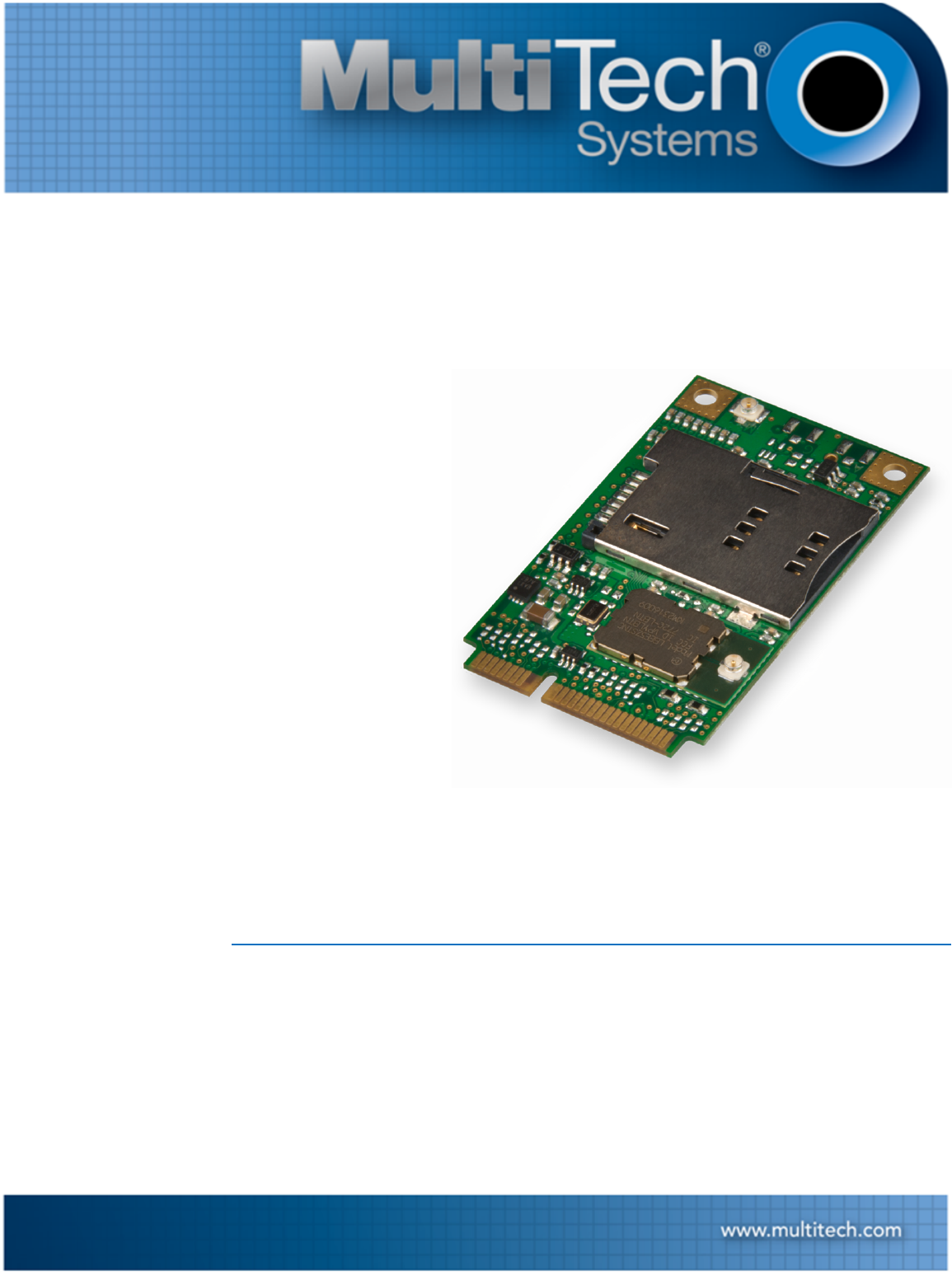
The MultiConnect™ PCIe embedded cellular modem is a complete, ready-to-integrate communications device that
offers standard-based penta-band HSPA+ 21, dual-band EV-DO Rev A, or CDMA performance. This quick-to-market
communications device allows developers to add wireless communication and GPS tracking to products with a
minimum of development time and expense. The MultiConnect PCIe embedded cellular modem is based on
industry-standard open interfaces and utilizes a PCI Express Mini Card form factor.
Documentation
The following documentation is available by email to oemsales@multitech.com or by using the Developer Guide
Request Form at www.multitech.com.
■MultiConnect PCIe Developer Guide – This document. Provides an overview, safety and regulatory
information, design considerations, schematics, and device information for developers.
■AT Command Guide – Device specific AT command reference guide.
Product Build Options
Product Description
MTPCIE-H5 HSPA+ Embedded Cellular Modem
MTPCIE-H5-V HSPA+ Embedded Cellular Modem with digital voice and GPS.
MTPCIE-H5-V-BW HSPA+ Embedded Cellular Modem with digital voice, GPS, Wi-Fi, and Bluetooth
MTPCIE-BW Wi-Fi and Bluetooth
Developer Kit
MTPCIE-DK Developer Kit
Note:
■These units ship without network activation.
■To connect them to the cellular network, you need a cellular account. For more information, refer to
Account Activation.
■GP devices have a dedicated GPS receiver.
■The complete product code may end in .Rx. For example, MTPCIE-H5.Rx, where R is revision and x is
the revision number.
■All builds can be ordered individually or in 50-packs.
Developer Kit Contents
Your Developer Kit (MTPCIE-DK1) includes the following:
Developer Board 1 - MTPCIE-DK Developer Board
Power Supply 1 - 100-240V 9V-1.7A power supply with removable blades, 1 - US blade/plug, 1 - EURO
blade/plug, 1 - UK blade/plug
6 MultiConnectTM PCIe MTPCIE-H5/MTPCIE-BW Developer Guide
PRODUCT OVERVIEW
Cables 1 - RS-232 DB9F-DB9M serial cable, 1 - RJ-45 Ethernet cable, 2 -USB cable 2 - SMA-to-UFL
antenna cables (1 - for cellular, 1 - for GPS) 1 - RSMA-to-UFL antenna cable for
Bluetooth/Wi-Fi
Antennas 1 - 3.3V magnetic GPS antenna , 1 - HEPTA band SMA antenna, 1 - 2.4GHz, dipole Wi-Fi
antenna
Customer Notices Modem activation notice
Additional One promotional screwdriver
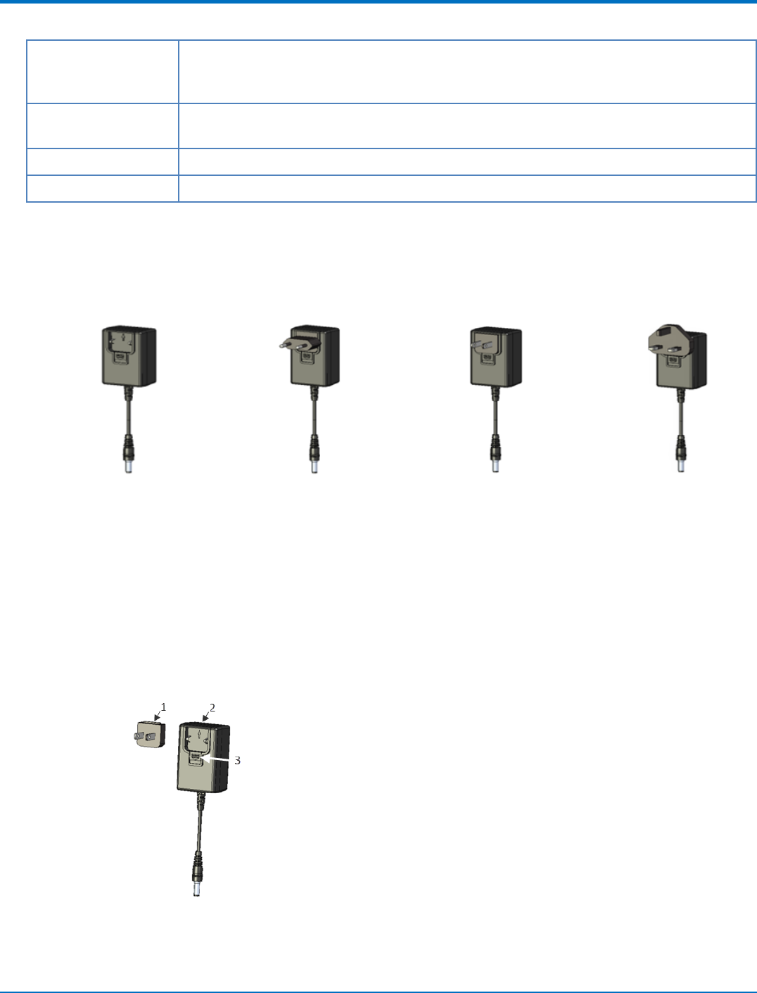
Attaching Power Supply Blades
Power Supply and Blades
If your device shipped with a power cord, attach the blades for your region.
Power Supply no Power Supply with Power Supply with Power Supply with
blades EU blade NAM blade UK blade
Attaching the Blades
To attach a power supply blade:
1. Remove the power supply cover (not shown). To do this, slide the lock down and hold it while you lift off
the cover.
2. Insert the latch on the blade into the notch on the power supply.
3. Slide the lock down and hold it while you press the blade in place. Then, release it.
1 - Latch
2 - Notch
3 - Sliding lock
MultiConnectTM PCIe MTPCIE-H5/MTPCIE-BW Developer Guide 7
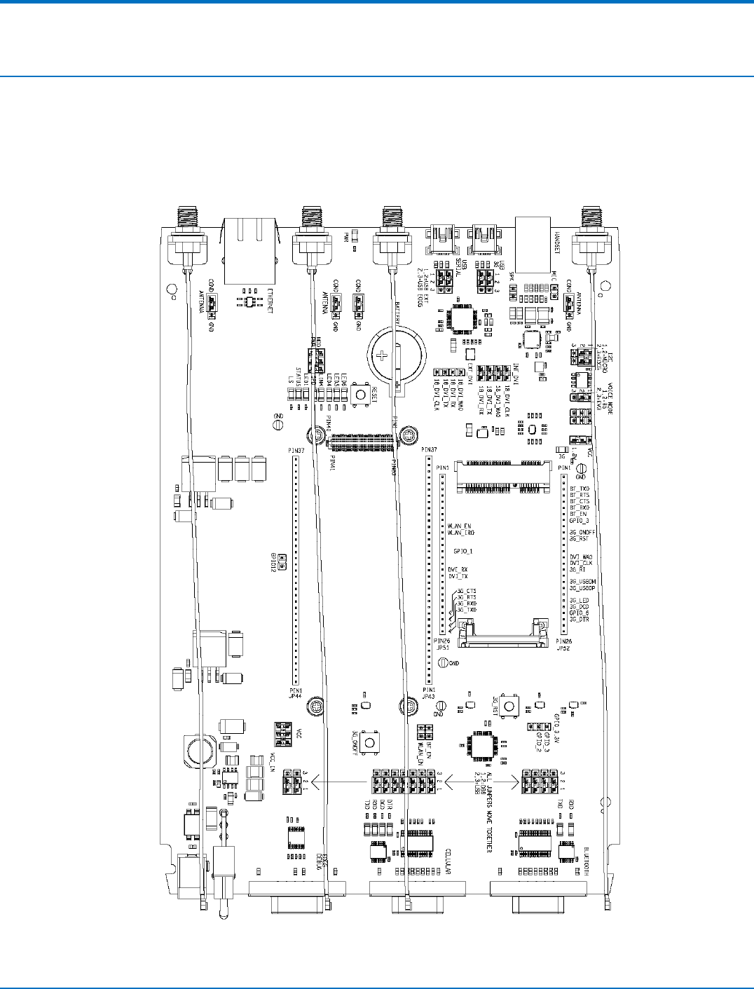
PINOUT
Pinout
Multi-Tech Mini PCIe Pinout
Note:
Some modems do not include all the pins shown above. Refer to your model’s Device Guide for model
specific pinout information.
SDIO can operate up to 25Mhz. Treat the SDIO traces to Host like a bus and keep the bus length as short as
possible. Multi-Tech recommends adding series termination resistors on all the SDIO traces.
Pin # Name I/O Function MTPCIE-H5 MTPCIE-H5-V-BW MTPCIE-
BW
1 SDIO_D0 I/O Wi-Fi SDIO_D0 X X
2 3.3Vaux I 3.3Vaux X X X
3 SDIO_D1 I/O Wi-Fi SDIO_D1 X X
4 GND Ground X X X
5 SDIO_D2 I/O Wi-Fi SDIO_D2 X X
6 BT_TXD I Bluetooth Transmit X X
data
7 SDIO_D3 I/O Wi-Fi SDIO_D3 X X
8 BT_RTS I Bluetooth RTS X X
9 GND Ground X X X
10 BT_CTS O Bluetooth CTS X X
11 SDIO_CMD I/O Wi-Fi SDIO_CMD X X
12 BT_RXD O Bluetooth Receive data X X
13 SDIO_CLK I Wi-Fi SDIO_CLK X X
14 BT_EN I Bluetooth enable (low X X
disable)
15 GND Ground X X X
16 GPIO_2 I/O 3G Cellular General X
purpose I/O
17 WLAN_EN I Wi-Fi enable (low X X
disable)
18 GND Ground X X X
19 WLAN_IRQ O Wi-Fi interrupt (low X X
active)
20 3G_ONOFF I 3G Cellular On/Off (low X X
active)
8 MultiConnectTM PCIe MTPCIE-H5/MTPCIE-BW Developer Guide

PINOUT
Pin # Name I/O Function MTPCIE-H5 MTPCIE-H5-V-BW MTPCIE-
BW
21 GND Ground X X X
22 3G_RST I 3G Cellular Reset line X X
(low active)
23 1.8V O 1.8V output X X
24 3.3Vaux I 3.3Vaux X X X
25 GPIO_1 I/O Bluetooth General X X
purpose I/O
26 GND Ground X X X
27 GND Ground X X X
28 3G_DVI_WA0 I/O 3G Cellular digital voice X
control line
29 GND Ground X X X
30 3G_DVI_CLK I/O 3G Cellular digital voice X
clock
31 3G_DVI_RX I 3G Cellular digital voice X
receive
32 RI O 3G Cellular UART RI X
33 3G_DVI_TX O 3G Cellular digital voice X
transmit
34 GND Ground X X X
35 GND Ground X X X
36 USB_D- I/O 3G USB Negative Data X X
37 GND Ground X X X
38 USB_D+ I/O 3G USB Positive Data X X
39 3.3Vaux I 3.3Vaux X X X
40 GND Ground X X X
41 3.3Vaux I 3.3Vaux X X X
42 LED_WWAN# O 3G Cellular STAT LED X X
Output
43 GND Ground X X X
44 DCD O 3G Cellular UART DCD X
45 CTS O 3G Cellular UART CTS X
46 GPIO_3 I/O 3G Celllular General X
purpose I/O
47 RTS I 3G Cellular UART RTS X
MultiConnectTM PCIe MTPCIE-H5/MTPCIE-BW Developer Guide 9

PINOUT
Pin # Name I/O Function MTPCIE-H5 MTPCIE-H5-V-BW MTPCIE-
BW
48 DTR I 3G Cellular UART DTR X
49 RXD O 3G Cellular UART X
Receive data
50 GND Ground X X X
51 TXD I 3G Cellular UART X
transmit data
52 3.3Vaux I 3.3Vaux X X X
10 MultiConnectTM PCIe MTPCIE-H5/MTPCIE-BW Developer Guide

PINOUT
Standard Mini-PCI Express Pinout
Pin # Function I/O Description
1 WAKE# O WAKE
2 3.3Vaux I 3.3Vaux
3 COEX1 I Co-existence pin, not defined
4 GND GND
5 COEX2 I Co-existence pin, not defined
6 1.5V I 1.5V
7 CLKREQ# O CLKREQ#
8 UIM_PWR I UIM_PWR
9 GND GND
10 UIM_DATA I/O UIM_DATA
11 REFCLK+ I PCI Express reference clock
12 UIM_CLK I UIM_CLK
13 REFCLK- I PCI Express reference clock
14 UIM_RESET I UIM_RESET
15 GND GND
16 UIM_VPP 0 UIM_VPP
17 Reserved Reserved
18 GND GND
19 Reserved Reserved
20 W_DISABLE# I W_DISABLE#
21 GND GND
22 PERST# I PERST#
23 PERn0 O PCI Express receiver differential pair signal
24 3.3Vaux I 3.3Vaux
25 PERp0 O PCI Express receiver differential pair signal
26 GND GND
27 GND GND
28 1.5V I 1.5V
29 GND GND
30 SMB_CLK I SMB_CLK
31 PETn0 I PCI Express transmitter differential pair signal
32 SMB_DATA I/O SMB_DATA
MultiConnectTM PCIe MTPCIE-H5/MTPCIE-BW Developer Guide 11

PINOUT
Pin # Function I/O Description
33 PETp0 I PCI Express transmitter differential pair signal
34 GND GND
35 GND GND
36 USB_D- I/O USB Negative Data
37 GND GND
38 USB_D+ I/O USB Positive Data
39 3.3Vaux I 3.3Vaux
40 GND GND
41 3.3Vaux I 3.3Vaux
42 LED_WWAN# O LED Output
43 GND GND
44 LED_WLAN# O LED Output
45 Reserved Reserved
46 LED_WPAN# O LED Output
47 Reserved Reserved
48 1.5V I 1.5V
49 Reserved Reserved
50 GND GND
51 Reserved Reserved
52 3.3Vaux I 3.3Vaux
12 MultiConnectTM PCIe MTPCIE-H5/MTPCIE-BW Developer Guide

PINOUT
Pinout for Cellular USB Only
Pin # Name I/O Description
2 3.3 Vaux I 3.3 Vaux
4 GND Ground
9 GND Ground
15 GND Ground
18 GND Ground
20 3G_ONOFF I 3G cellular on/off
21 GND Ground
22 3G_RST I 3G cellular reset line
24 3.3 Vaux I 3.3 Vaux
26 GND Ground
27 GND Ground
29 GND Ground
35 GND Ground
36 USB_D- I/O 3G USB Negative Data
37 GND Ground
38 USB_D+ I/O 3G USB Positive Data
39 3.3 Vaux I 3.3 Vaux
40 GND Ground
41 3.3 Vaux I 3.3 Vaux
42 LED_WWAN O 3G Cellular STAT LED Output
43 GND Ground
50 GND Ground
52 3.3 Vaux I 3.3 Vaux
MultiConnectTM PCIe MTPCIE-H5/MTPCIE-BW Developer Guide 13

DESIGN CONSIDERATIONS
Design Considerations
Design Consideration
When using the Multi-Tech MiniPCIe form factor:
■Consult your modem’s device guide for device dimensions. With the modem, the Multi-Tech Mini PCIe form
factor exceeds the standard Mini PCIe maximum component height for top and bottom.
■If you need to install components under the module, use taller connectors to avoid conflict. Multi-Tech
recommends not installing components under the module.
■Check the Pinout table for pins that differ from the MiniPCIe spec.
Noise Suppression Design
Adhere to engineering noise-suppression practices when designing a printed circuit board (PCB) containing the
MultiConnect PCIe. Noise suppression is essential to the proper operation and performance of the modem and
surrounding equipment.
Any OEM board design that contains the MultiConnect PCIe must consider both on-board and off-board generated
noise that can affect digital signal processing. Both on-board and off-board generated noise that is coupled on-
board can affect interface signal levels and quality. Noise in frequency ranges that affect modem performance is of
particular concern.
On-board generated electromagnetic interference (EMI) noise that can be radiated or conducted off-board is
equally important. This type of noise can affect the operation of surrounding equipment. Most local government
agencies have certification requirements that must be met for use in specific environments.
Proper PC board layout (component placement, signal routing, trace thickness and geometry, and so on)
component selection (composition, value, and tolerance), interface connections, and shielding are required for the
board design to achieve desired modem performance and to attain EMI certification.
Other aspects of proper noise-suppression engineering practices are beyond the scope of this guide. Consult noise
suppression techniques described in technical publications and journals, electronics and electrical engineering text
books, and component supplier application notes.
PC Board Layout Guideline
In a 4-layer design, provide adequate ground plane covering the entire board. In 4-layer designs, power and ground
are typically on the inner layers. Ensure that all power and ground traces are 0.05 inches wide.
Electromagnetic Interference
The following guidelines are offered specifically to help minimize EMI generation. Some of these guidelines are the
same as, or similar to, the general guidelines. To minimize the contribution of device-based design to EMI, you
must understand the major sources of EMI and how to reduce them to acceptable levels.
■Keep traces carrying high frequency signals as short as possible.
■Provide a good ground plane or grid. In some cases, a multilayer board may be required with full layers for
ground and power distribution.
■Decouple power from ground with decoupling capacitors as close to the device's power pins as possible.
14 MultiConnectTM PCIe MTPCIE-H5/MTPCIE-BW Developer Guide

DESIGN CONSIDERATIONS
■Eliminate ground loops, which are unexpected current return paths to the power source and ground.
■Decouple the power cord at the power cord interface with decoupling capacitors. Methods to decouple
power lines are similar to decoupling telephone lines.
■Locate high frequency circuits in a separate area to minimize capacitive coupling to other circuits.
■Locate cables and connectors to avoid coupling from high frequency circuits.
■Lay out the highest frequency signal traces next to the ground grid.
■If using a multilayer board design, make no cuts in the ground or power planes and be sure the ground
plane covers all traces.
■Minimize the number of through-hole connections on traces carrying high frequency signals.
■Avoid right angle turns on high frequency traces. Forty-five degree corners are good; however, radius turns
are better.
■On 2-layer boards with no ground grid, provide a shadow ground trace on the opposite side of the board to
traces carrying high frequency signals. This will be effective as a high frequency ground return if it is three
times the width of the signal traces.
■Distribute high frequency signals continuously on a single trace rather than several traces radiating from
one point.
Electrostatic Discharge Control
Handle all electronic devices with precautions to avoid damage due to the static charge accumulation.
See the ANSI/ESD Association Standard (ANSI/ESD S20.20-1999) – a document “for the Development of an
Electrostatic Discharge Control for Protection of Electrical and Electronic Parts, Assemblies and Equipment.” This
document covers ESD Control Program Administrative Requirements, ESD Training, ESD Control Program Plan
Technical Requirements (grounding/bonding systems, personnel grooming, protected areas, packaging, marking,
equipment, and handling), and Sensitivity Testing.
Multi-Tech strives to follow these recommendations. Input protection circuitry is incorporated in Multi-Tech
devices to minimize the effect of static buildup. Take precautions to avoid exposure to electrostatic discharge
during handling.
Multi-Tech uses and recommends that others use anti-static boxes that create a faraday cage (packaging designed
to exclude electromagnetic fields). Multi-Tech recommends that you use our packaging when returning a product
and when you ship your products to your customers.
USB Design
Multi-Tech recommends that you review Intel's High Speed USB Platform Design Guidelines for information about
USB signal routing, impedance, and layer stacking. Also:
■Shield USB cables with twisted pairs (especially those containing D+/D-).
■Use a single 5V power supply for USB devices. See the Power Draw section in your model’s Device Guide for
current (ampere) requirements.
■Route D+/D- together in parallel with the trace spacing needed to achieve 90 ohms differential impedance
for the USB pair and to maintain a 20 mil space from the USB pair and all other signals.
■If power is provided externally, use a common ground between the carrier board and the device.
MultiConnectTM PCIe MTPCIE-H5/MTPCIE-BW Developer Guide 15
DEVELOPER BOARD AND SCHEMATICS
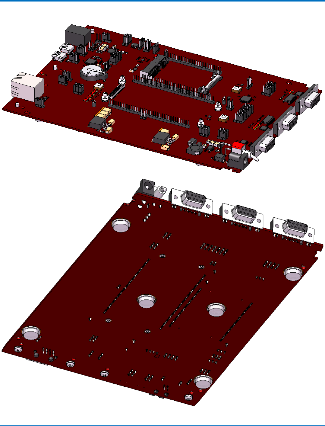
Developer Board and Schematics
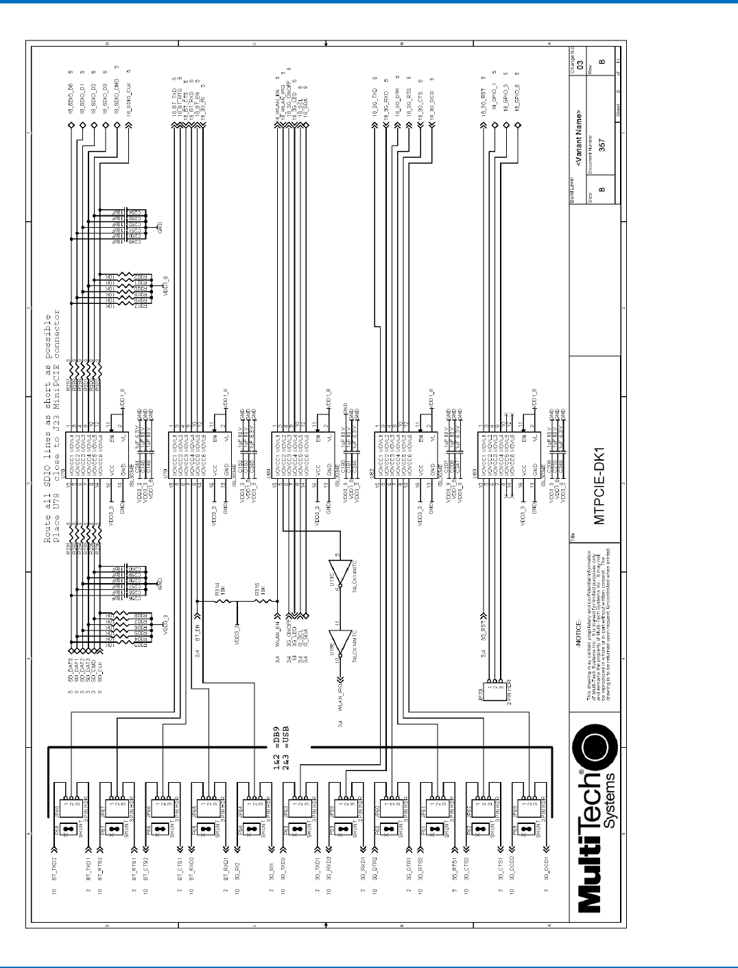
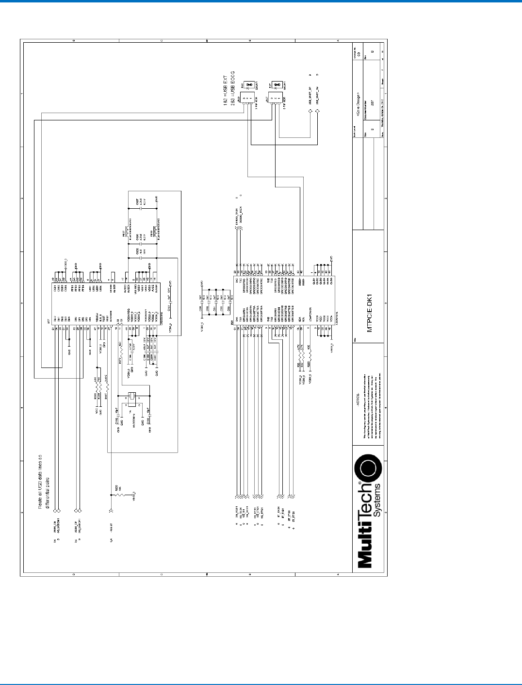
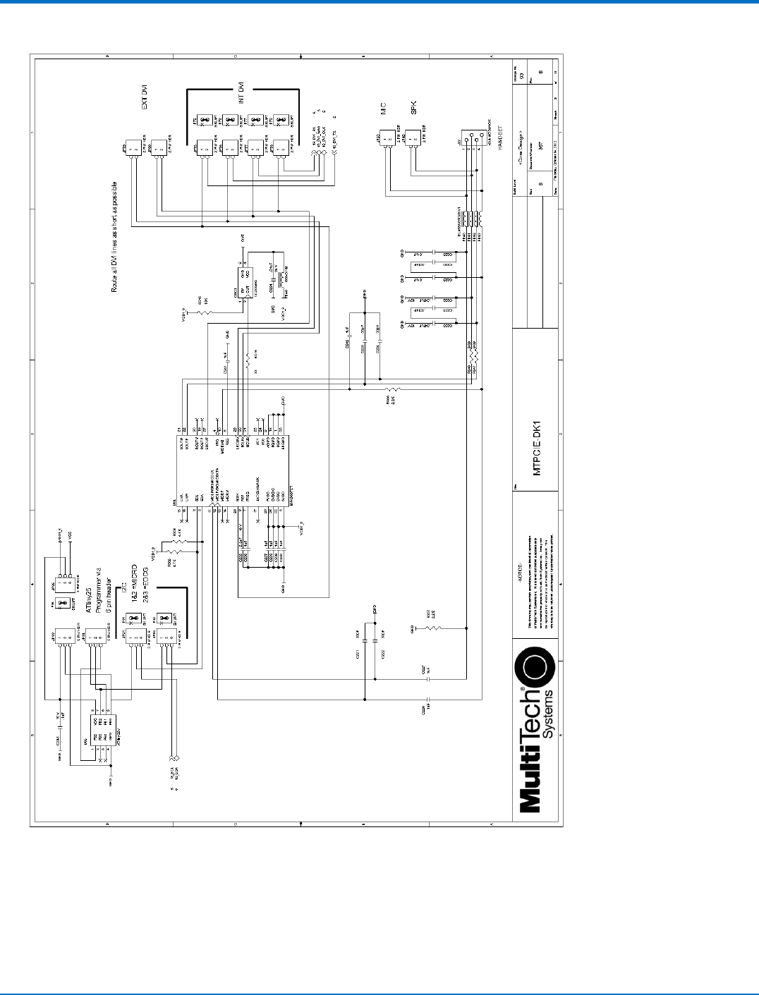
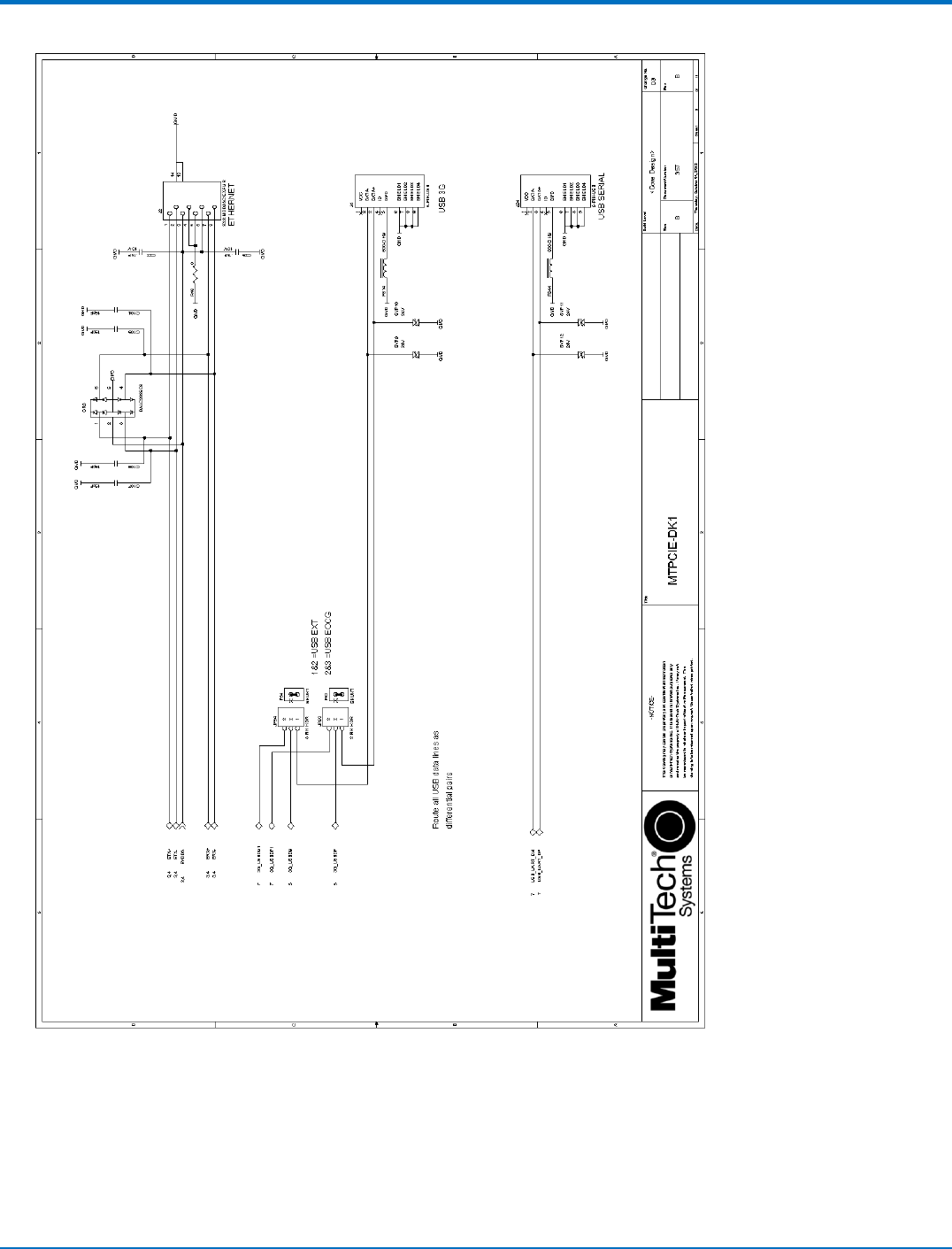
Note: Third-party components shown in the following drawings are included as examples only.
Developer Board
This developer board drawing shows the major board components.
16 MultiConnectTM PCIe MTPCIE-H5/MTPCIE-BW Developer Guide
DEVELOPER BOARD AND SCHEMATICS
MultiConnectTM PCIe MTPCIE-H5/MTPCIE-BW Developer Guide 17
DEVELOPER BOARD AND SCHEMATICS
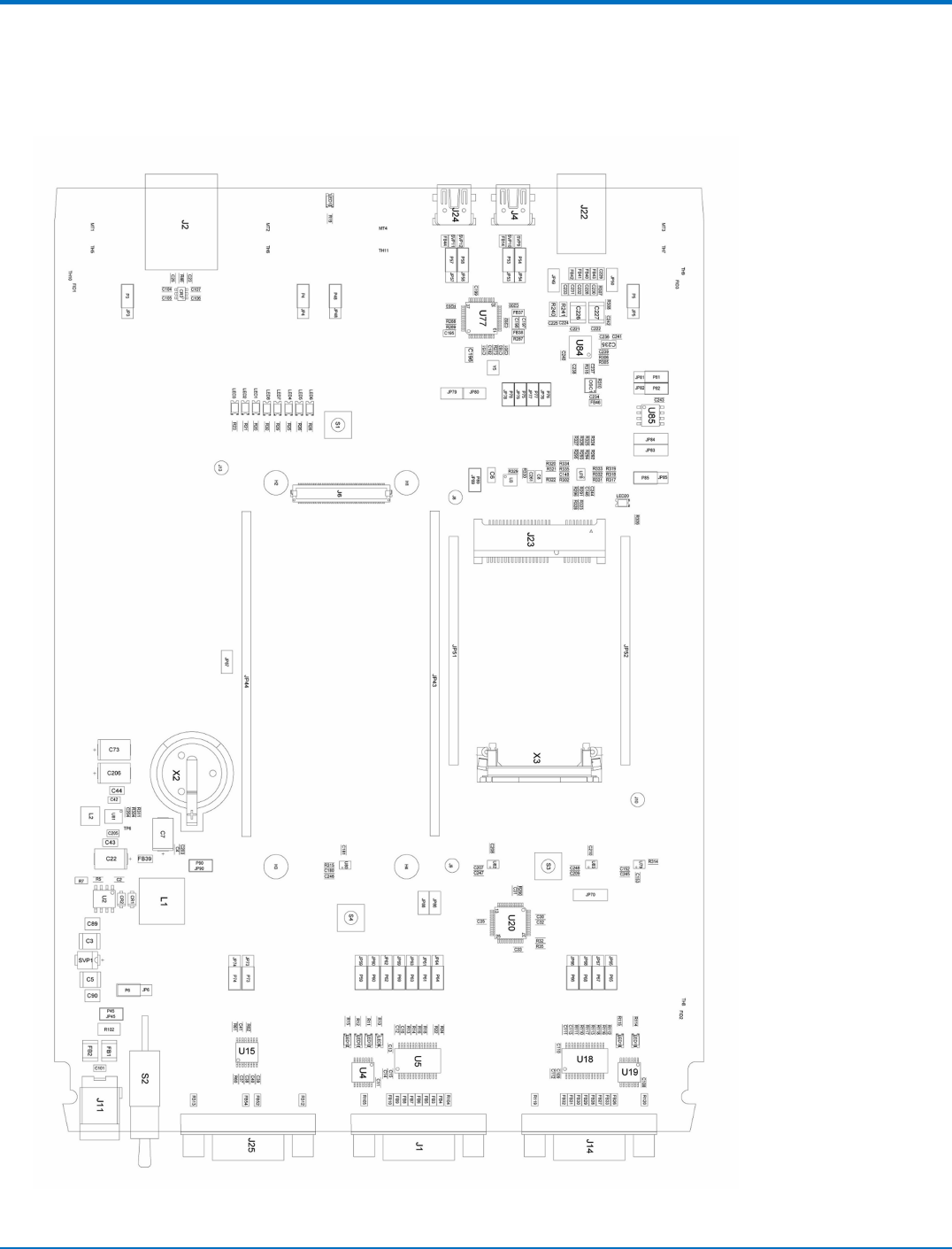
Assembly Diagram
Top
18 MultiConnectTM PCIe MTPCIE-H5/MTPCIE-BW Developer Guide

DEVELOPER BOARD AND SCHEMATICS
Bottom
MultiConnectTM PCIe MTPCIE-H5/MTPCIE-BW Developer Guide 19
DEVELOPER BOARD AND SCHEMATICS
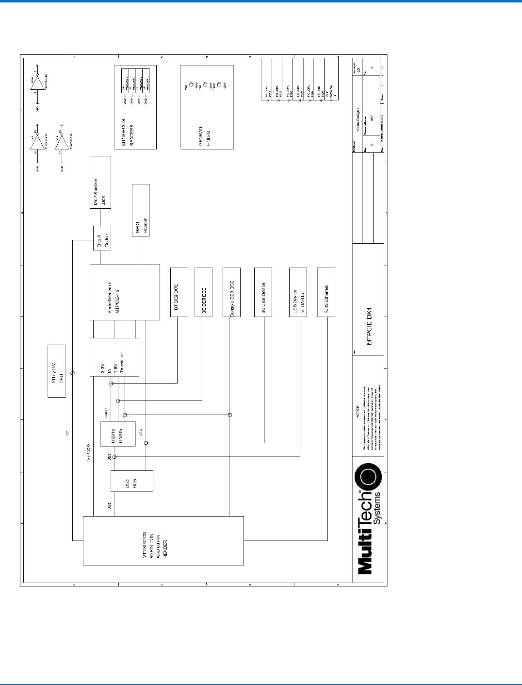
Developer Board Block Diagram
20 MultiConnectTM PCIe MTPCIE-H5/MTPCIE-BW Developer Guide
DEVELOPER BOARD AND SCHEMATICS
Developer Board Schematics
MultiConnectTM PCIe MTPCIE-H5/MTPCIE-BW Developer Guide 21
DEVELOPER BOARD AND SCHEMATICS
22 MultiConnectTM PCIe MTPCIE-H5/MTPCIE-BW Developer Guide
DEVELOPER BOARD AND SCHEMATICS
MultiConnectTM PCIe MTPCIE-H5/MTPCIE-BW Developer Guide 23
DEVELOPER BOARD AND SCHEMATICS
24 MultiConnectTM PCIe MTPCIE-H5/MTPCIE-BW Developer Guide
DEVELOPER BOARD AND SCHEMATICS
MultiConnectTM PCIe MTPCIE-H5/MTPCIE-BW Developer Guide 25
DEVELOPER BOARD AND SCHEMATICS
26 MultiConnectTM PCIe MTPCIE-H5/MTPCIE-BW Developer Guide
DEVELOPER BOARD AND SCHEMATICS
MultiConnectTM PCIe MTPCIE-H5/MTPCIE-BW Developer Guide 27
DEVELOPER BOARD AND SCHEMATICS
28 MultiConnectTM PCIe MTPCIE-H5/MTPCIE-BW Developer Guide
DEVELOPER BOARD AND SCHEMATICS
MultiConnectTM PCIe MTPCIE-H5/MTPCIE-BW Developer Guide 29

DEVELOPER BOARD AND SCHEMATICS
Board Components
Jumper Description
JP3, JP4, JP5, JP48 Selects CGND or GND for antenna holder grounding. Default is CGND.
JP6 JP6 allows you to select either the internal 5V regulator (INT PWR) or to choose EXT
5V (EXT PWR). For the EXT PWR, you can use your own external 5V power source
and plug it into J11.
JP43, JP44 Not used by PCIe devices.
JP45 Board Power. Default is installed.
JP49 Probes for connecting speaker.
JP50 Probes for connecting microphone.
JP51, JP52 Debugging probes for PCIE connector J23.
JP53, JP54 Selects USB host connected to PCIe device. Pins 1 & 2 jumpered selects external USB
host connected to J4.
JP57, JP58 Selects USB host connected to quad serial UART U20. Pins 1 & 2 jumpered selects
external USB host connected to J24.
JP59, JP60, JP61,JP63,JP64, Selects serial connection for PCIe device. Pins 1 & 2 jumpered selects DB9 connector
JP69 J1 connected to PCIe device. Pins 2 & 3 jumpered selects quad UART U20 connected
to PCIe device. All jumpers must be moved to the same position.
JP65, JP66, JP67, JP68 Selects serial connection for PCIe Bluetooth device. Pins 1 & 2 jumpered selects DB9
connector J14 connected to PCIe Bluetooth device. Pins 2 & 3 jumpered selects quad
UART U20 connected to PCIe Bluetooth device. All jumpers must be moved to the
same position.
JP70 Probes for PCIe GPIO2 & GPIO3. The pin next to the text "GPIO_3.3V" is GPIO3. The
center pin is GPIO2.
JP73, JP74 Not used by PCIe devices.
JP75, JP76, JP77, JP78 When these jumpers are installed, DVI interface of audio codec U84 is connected to
DVI interface of PCIe device. By removing these jumpers when connecting an
external DVI device.
JP79, JP80 Use these jumper pins to connect an external DVI device.
JP81, J82 Selects source for programming audio codec U84. Pins 1 & 2 jumpered selects
MICRO U84 as source. Default is MICRO.
JP83, JP84 These pins can be used for programming MICRO U84.
JP85 Selects power source for MICRO U85. Default is 1.8v
JP86 May be used to manually reset PCIe Bluetooth device by briefly installing and then
removing a jumper. Default is no jumper installed.
JP87 Not applicable for this device.
JP88 May be used to manually reset PCIe Wi-Fi device by briefly installing and then
removing a jumper. Default is no jumper installed.
JP89 This jumper, when installed, connects power to PCIe device.
30 MultiConnectTM PCIe MTPCIE-H5/MTPCIE-BW Developer Guide
DEVELOPER BOARD AND SCHEMATICS
Jumper Description
JP90 Not used by PCIe device.This jumper, when installed, connects power to OCG-E
device. (When using Developer Kit with OCG-E devices).
J6 Not used by PCIe device.
J23 Socket for installing PCIe device.
J8, J9, J10, J13 Oscilloscope probe ground connections
S1 Not used by PCIe device.
S3 Reset button for PCIe device.
S4 Button for on/off of PCIe.
Installing a Communications Device onto the Board
To install a device on the board:
1. Align the device pin with Pin 1 of the socket connector on the board and press firmly.
2. Use the optional antenna lead to connect to the device's antenna connector.
Installing a SIM Card
To install a SIM card:
■Install the SIM card into the SIM card holder on the radio.
MultiConnectTM PCIe MTPCIE-H5/MTPCIE-BW Developer Guide 31

SAFETY NOTICES AND WARNINGS
Safety Notices and Warnings
The following safety statements may be relevant and required in the host product literature.
Radio Frequency (RF) Safety
Due to the possibility of radio frequency (RF) interference, it is important that you follow any special regulations
regarding the use of radio equipment. Follow the safety advice given below.
■Operating your device close to other electronic equipment may cause interference if the equipment is
inadequately protected. Observe any warning signs and manufacturers’ recommendations.
■Different industries and businesses restrict the use of cellular devices. Respect restrictions on the use of
radio equipment in fuel depots, chemical plants, or where blasting operations are in process. Follow
restrictions for any environment where you operate the device.
■Do not place the antenna outdoors.
■Switch OFF your wireless device when in an aircraft. Using portable electronic devices in an aircraft may
endanger aircraft operation, disrupt the cellular network, and is illegal. Failing to observe this restriction
may lead to suspension or denial of cellular services to the offender, legal action, or both.
■Switch OFF your wireless device when around gasoline or diesel-fuel pumps and before filling your vehicle
with fuel.
■Switch OFF your wireless device in hospitals and any other place where medical equipment may be in use.
Sécurité des fréquences radio
En raison de la possibilité d'interférences de radiofréquence (RF), il est important que vous suiviez une quelconque
réglementation concernant l'utilisation du matériel radio. Suivez les conseils de sécurité ci-dessous.
■Fonctionnement de votre appareil à proximité d'autres appareils électroniques peuvent causer des
interférences si l'équipement est insuffisamment protégé. Respectez les panneaux d'avertissement et les
recommandations du fabricant.
■Différentes industries et les entreprises limitent l'utilisation des appareils cellulaires. Respectez les
règlements sur l'utilisation des équipements radio dans les dépôts de carburant, les usines chimiques, ou
lorsque des opérations de dynamitage sont en cours. Suivez restrictions pour n'importe quel environnement
où vous utilisez l'appareil.
■Ne pas placer l'antenne à l'extérieur.
■Éteignez votre appareil sans fil dans un avion. Utilisant des dispositifs électroniques portables dans un avion
peut mettre en danger le fonctionnement de l'avion, peut perturber le réseau cellulaire, et est illégal. Le
non-respect de cette restriction peut entraîner la suspension ou le refus des services cellulaires au
contrevenant, une action en justice, ou les deux.
■Éteignez votre appareil sans fil lorsque autour de l'essence ou pompes diesel-carburant et avant de remplir
votre véhicule avec du carburant.
■Éteignez votre appareil sans fil dans les hôpitaux et tout autre endroit où l'équipement médical peut être
utilisé.
Vehicle Safety
When using your device in a vehicle:
32 MultiConnectTM PCIe MTPCIE-H5/MTPCIE-BW Developer Guide

SAFETY NOTICES AND WARNINGS
■Do not use this device while driving.
■Respect national regulations on the use of cellular devices in vehicles.
■If incorrectly installed in a vehicle, operating the wireless device could interfere with the vehicle’s
electronics. To avoid such problems, use qualified personnel to install the device. The installer should verify
the vehicle electronics are protected from interference.
■Using an alert device to operate a vehicle’s lights or horn is not permitted on public roads.
■UL evaluated this device for use in ordinary locations only. UL did NOT evaluate this device for installation in
a vehicle or other outdoor locations. UL Certification does not apply or extend to use vehicles or outdoor
applications or in ambient temperatures above 40° C.
User Responsibility
Respect all local regulations for operating your wireless device. Use the security features to block unauthorized use
and theft.
Device Maintenance
When maintaining your device:
■Do not attempt to disassemble the device. There are no user serviceable parts inside.
■Do not expose your device to any extreme environment where the temperature or humidity is high.
■Do not expose the device to water, rain, or spilled beverages. It is not waterproof.
■Do not place the device alongside computer discs, credit or travel cards, or other magnetic media. The
information contained on discs or cards may be affected by the device.
■Using accessories, such as antennas, that Multi-Tech has not authorized or that are not compliant with
Multi-Tech's accessory specifications may invalidate the warranty.
If the device is not working properly, contact Multi-Tech Technical Support.
Notice regarding Compliance with FCC and Industry Canada
Requirements for RF Exposure
The antenna intended for use with this unit meets the requirements for mobile operating configurations and for
fixed mounted operations, as defined in 2.1091 of the FCC rules for satisfying RF exposure compliance. If an
alternate antenna is used, consult user documentation for required antenna specifications.
Compliance of the device with the FCC and IC rules regarding RF Exposure was established and is given with the
maximum antenna gain as specified above for a minimum distance of 20 cm between the devices radiating
structures (the antenna) and the body of users. Qualification for distances closer than 20 cm (portable operation)
would require re-certification.
MultiConnectTM PCIe MTPCIE-H5/MTPCIE-BW Developer Guide 33
LABELING REQUIREMENTS
Labeling Requirements
Approvals and Certification
Your Multi-Tech device is an industry and/or carrier approved modem.
■PTCRB Requirements (GPRS and HSPA/HSDPA only).
The antenna system cannot be altered. If altered, additional PTCRB testing may be required.
■For HSPA+, HSPA, HSDPA and GPRS Devices
The modem's 15-character IMEI (International Mobile Equipment Identity) number is printed on the
modem's label.
Example HSPA+ H5 Labels
Note: Actual labels will vary depending on the regulatory approval markings and content.
This device complies with part 15 of the FCC Rules. Operation is subject to the following two conditions: (1) This
device may not cause harmful interference, and (2) this device must accept any interference received, including
interference that may cause undesired operation.
The label shown is larger than actual size.
1 - Multi-Tech Model Identification.
2 - Multi-Tech Ordering Part Number.
3 - IMEI (International Mobile Equipment
Identity).
34 MultiConnectTM PCIe MTPCIE-H5/MTPCIE-BW Developer Guide
LABELING REQUIREMENTS
Labels are positioned on the device as follows:
Host Labeling
The following statements are required to be on the host label:
■This device contains FCC ID: {Add the FCC ID of the specific device}
■This device contains equipment certified under IC ID: {Add the IC ID of the specific device}
MultiConnectTM PCIe MTPCIE-H5/MTPCIE-BW Developer Guide 35
REGULATORY STATEMENTS
Regulatory Statements
R&TTE Directive Compliance
The CE mark is affixed to this product to confirm compliance with the following European Community Directives:
Council Directive 2004/108/EC of 15 December 2004 on the approximation of the laws of Member States
relating to electromagnetic compatibility;
and
Council Directive 2006/95/EC of 12 December 2006 on the harmonization of the laws of Member States
relating to electrical equipment designed for use within certain voltage limits;
and
Council Directive 1999/5/EC of 9 March 1999 on radio equipment and telecommunications terminal
equipment and the mutual recognition of their conformity.
RF spectrum use (R&TTE art. 3.2) EN 301 511 V9.0.2
EN 300 440-2 V1.4.1
EMC (R&TTE art. 3.1b) EN 301 489-1 V1.9.2
EN 301 489-3 V1.4.1
EN 301 489-7 V1.3.1
Health & Safety (R&TTE art. 3.1a) EN 60950-1:2006 + A11:2009 + A1:2010 + A12:2011 + AC:2011
EN 62311:2008
36 MultiConnectTM PCIe MTPCIE-H5/MTPCIE-BW Developer Guide

REGULATORY STATEMENTS
Restriction of the Use of Hazardous Substances (RoHS)
Multi-Tech Systems, Inc
Certificate of Compliance
2011/65/EU
Multi-Tech Systems confirms that its embedded products comply with the chemical concentration limitations set
forth in the directive 2011/65/EU of the European Parliament (Restriction of the use of certain Hazardous
Substances in electrical and electronic equipment - RoHS).
These Multi-Tech products do not contain the following banned chemicals1:
■Lead, [Pb] < 1000 PPM
■Mercury, [Hg] < 1000 PPM
■Hexavalent Chromium, [Cr+6] < 1000 PPM
■Cadmium, [Cd] < 100 PPM
■Polybrominated Biphenyl, [PBB] < 1000 PPM
■Polybrominated Diphenyl Ether, [PBDE] < 1000 PPM
Environmental considerations:
■Moisture Sensitivity Level (MSL) =1
■Maximum Soldering temperature = 260C (in SMT reflow oven)
1Lead usage in some components is exempted by the following RoHS annex, therefore higher lead concentration
would be found in some modules (>1000 PPM);
- Resistors containing lead in a glass or ceramic matrix compound.
International Modem Restrictions
Some dialing and answering defaults and restrictions may vary for international modems. Changing settings may
cause a modem to become non-compliant with national regulatory requirements in specific countries. Also note
that some software packages may have features or lack restrictions that may cause the modem to become non-
compliant.
Industry Canada and FCC
This device complies with Industry Canada licence-exempt RSS standard(s) and part 15 of the FCC rules. Operation
is subject to the following two conditions:
(1) this device may not cause interference, and
(2) this device must accept any interference, including interference that may cause undesired operation of the
device.
Cet appareil est conforme avec Industrie Canada RSS exemptes de licence standard (s) et la partie 15 des règles de
la FCC. Son fonctionnement est soumis aux deux conditions suivantes:
MultiConnectTM PCIe MTPCIE-H5/MTPCIE-BW Developer Guide 37
REGULATORY STATEMENTS
1. l'appareil ne doit pas produire de brouillage, et
2. l'utilisateur de l'appareil doit accepter tout brouillage radioélectrique subi, même si le brouillage est susceptible
d'en compromettre le fonctionnement.
Warning: Changes or modifications to this radio device not expressly approved by the party responsible for
compliance could void the user’s authority to operate the equipment.
Note: In Wi-Fi operation, the modem cannot operate on Channels 12, 13, or 14 due to FCC regulations.
Requirements for Cellular Antennas with regard to FCC/IC Compliance
Alterations to the antenna system may require additional testing at a certified lab. The antenna system must
maintain the same specifications. The antenna must be the same type, with similar in-band and out-of-band
radiation patterns.
This device has been designed to operate with the antennas listed below and having a maximum gain for 850 Mhz
of <= 6.4 dBi , for 1700 Mhz of <= 6.5 dBi, and for 1900 Mhz of <= 3 dBi. Antennas not included in this list or that
have a gain greater than specified are strictly prohibited for use with this device. The required antenna impedance
is 50 ohms.
Industry Canada and FCC Identification Numbers
Additional device information is available on the Industry Canada and FCC websites.
Model Canada ID FCC ID
MTPCIE-H5 125A-0047 AU792U12616852
MTPCIE-H5-V 125A-0047 AU792U12616852
MTPCIE-H5-V-BW 125A-0048 AU792U12616836
38 MultiConnectTM PCIe MTPCIE-H5/MTPCIE-BW Developer Guide
ENVIRONMENTAL NOTICES
Environmental Notices
Waste Electrical and Electronic Equipment Statement
Note: This statement may be used in documentation for your final product applications.
WEEE Directive
The WEEE Directive places an obligation on EU-based manufacturers, distributors, retailers, and importers to take-
back electronics products at the end of their useful life. A sister directive, ROHS (Restriction of Hazardous
Substances) complements the WEEE Directive by banning the presence of specific hazardous substances in the
products at the design phase. The WEEE Directive covers all Multi-Tech products imported into the EU as of August
13, 2005. EU-based manufacturers, distributors, retailers and importers are obliged to finance the costs of recovery
from municipal collection points, reuse, and recycling of specified percentages per the WEEE requirements.
Instructions for Disposal of WEEE by Users in the European Union
The symbol shown below is on the product or on its packaging, which indicates that this product must not be
disposed of with other waste. Instead, it is the user's responsibility to dispose of their waste equipment by handing
it over to a designated collection point for the recycling of waste electrical and electronic equipment. The separate
collection and recycling of your waste equipment at the time of disposal will help to conserve natural resources
and ensure that it is recycled in a manner that protects human health and the environment. For more information
about where you can drop off your waste equipment for recycling, please contact your local city office, your
household waste disposal service or where you purchased the product.
July, 2005
MultiConnectTM PCIe MTPCIE-H5/MTPCIE-BW Developer Guide 39
ENVIRONMENTAL NOTICES
Information on HS/TS Substances According to Chinese Standards
In accordance with China's Administrative Measures on the Control of Pollution Caused by Electronic Information
Products (EIP) # 39, also known as China RoHS, the following information is provided regarding the names and
concentration levels of Toxic Substances (TS) or Hazardous Substances (HS) which may be contained in Multi-Tech
Systems Inc. products relative to the EIP standards set by China's Ministry of Information Industry (MII).
Hazardous/Toxic Substance/Elements
Name of the Component Lead Mercury Cadmium Hexavalent Polybromi Polybrominat
(PB) (Hg) (CD) Chromium nated ed Diphenyl
(CR6+) Biphenyl Ether (PBDE)
(PBB)
Printed Circuit Boards O O O O O O
Resistors X O O O O O
Capacitors X O O O O O
Ferrite Beads O O O O O O
Relays/Opticals O O O O O O
ICs O O O O O O
Diodes/ Transistors O O O O O O
Oscillators and Crystals X O O O O O
Regulator O O O O O O
Voltage Sensor O O O O O O
Transformer O O O O O O
Speaker O O O O O O
Connectors O O O O O O
LEDs O O O O O O
Screws, Nuts, and other X O O O O O
Hardware
AC-DC Power Supplies O O O O O O
Software /Documentation CDs O O O O O O
Booklets and Paperwork O O O O O O
Chassis O O O O O O
XRepresents that the concentration of such hazardous/toxic substance in all the units of homogeneous
material of such component is higher than the SJ/Txxx-2006 Requirements for Concentration Limits.
ORepresents that no such substances are used or that the concentration is within the aforementioned limits.
40 MultiConnectTM PCIe MTPCIE-H5/MTPCIE-BW Developer Guide
ENVIRONMENTAL NOTICES
Information on HS/TS Substances According to Chinese Standards (in
Chinese)
依依照照中中国国标标准准的的有有毒毒有有害害物物质质信信息息
根据中华人民共和国信息产业部 (MII) 制定的电子信息产品 (EIP) 标准-中华人民共和国《电子信息产品污染
控制管理办法》(第 39 号),也称作中国 RoHS, 下表列出了 Multi-Tech Systems, Inc. 产品中可能含有的有毒
物质 (TS) 或有害物质 (HS) 的名称及含量水平方面的信息。
有有害害//有有毒毒物物质质//元元素素
成成分分名名称称 铅铅 (PB) 汞汞 (Hg) 镉镉 (CD) 六六价价铬铬 (CR6+) 多多溴溴联联苯苯 多多溴溴二二苯苯醚醚
(PBB) (PBDE)
印刷电路板 O O O O O O
电阻器 X O O O O O
电容器 X O O O O O
铁氧体磁环 O O O O O O
继电器/光学部件 O O O O O OO
ICs O O O O O O
二极管/晶体管 O O O O O O
振荡器和晶振 X O O O O O
调节器 O O O O O O
电压传感器 O O O O O O
变压器 O O O O O O
扬声器 O O O O O O
连接器 O O O O O O
LEDs O O O O O O
螺丝、螺母以及其它五金件 X O O O O O
交流-直流电源 O O O O O O
软件/文档 CD O O O O O O
手册和纸页 O O O O O O
底盘 O O O O O O
X表示所有使用类似材料的设备中有害/有毒物质的含量水平高于 SJ/Txxx-2006 限量要求。
O表示不含该物质或者该物质的含量水平在上述限量要求之内。
MultiConnectTM PCIe MTPCIE-H5/MTPCIE-BW Developer Guide 41

ANTENNAS, CABLES, GPS
Antennas, Cables, GPS
Antenna System Cellular Devices
The cellular/wireless performance depends on the implementation and antenna design. The integration of the
antenna system into the product is a critical part of the design process; therefore, it is essential to consider it early
so the performance is not compromised. If changes are made to the device's certified antenna system, then
recertification will be required by specific network carriers.
FCC and IC Antenna Requirements Toward License Exempt Radio Transmitters
(Bluetooth/Wlan)
The license-exempt Blutooth/WLAN radio transmitter contained in this equipment may only be operated with an
antenna of a type, a maximum gain and the required antenna impedance as approved and specified below. To
reduce potential radio interference to other users, choose the antenna type and it's gain so that the equivalent
isotropically radiated power (EIRP) is not more than that necessary for successful communication.
Notice regarding Compliance with FCC and Industry Canada Requirements for RF
Exposure
The antenna intended for use with this unit meets the requirements for mobile operating configurations and for
fixed mounted operations, as defined in 2.1091 of the FCC rules for satisfying RF exposure compliance. If an
alternate antenna is used, consult user documentation for required antenna specifications.
Compliance of the device with the FCC and IC rules regarding RF Exposure was established and is given with the
maximum antenna gain as specified above for a minimum distance of 20 cm between the devices radiating
structures (the antenna) and the body of users. Qualification for distances closer than 20 cm (portable operation)
would require re-certification.
Cellular Antenna Information
3G Authorized Antennas
The cellular radio portion was approved with the following antenna:
Manufacturer: Laird Technologies.
Description: HEPTA-SM
Model Number: MAF94300
Multi-Tech ordering information:
Model Quantity
ANHB-1HRA 1
ANHB-10HRA 10
ANHB-50HRA 50
42 MultiConnectTM PCIe MTPCIE-H5/MTPCIE-BW Developer Guide
ANTENNAS, CABLES, GPS
3G Antenna Requirements/Specifications
Category Description
Frequency Range 824 – 960 MHz / 1710 – 1990 MHz / 1920 – 2170 MHz
Impedance 50 Ohms
VSWR VSWR should not exceed 2.0:1 at any point across the bands of operation
Typical Radiated Gain 850 MHz 3.17 dBi
950 MHz 3.51 dBi
1800 MHz 3.55 dBi
1900 MHz 3.0 dBi
2100 MHz 3.93 dBi
Radiation Omni-directional
Polarization Linear Vertical
Antenna Cable Information
Use the following UFL to SMA RF cable to connect the device to the antenna.
Description: Coax SMA to UFL 8.5inch (216mm)
Multi-Tech Part Number: 45009575L
Multi-Tech ordering information:
Model Quantity
CASMA-UFL-1 1
CASMA-UFL-10 10
CASMA-UFL-50 50
Average Cable Loss
The table shows the average cable loss for each cell band.
Band Loss
800 0.37
MultiConnectTM PCIe MTPCIE-H5/MTPCIE-BW Developer Guide 43
ANTENNAS, CABLES, GPS
Band Loss
900 0.40
1800 0.70
1900 0.63
2100 0.70
GPS Antennas
GPS Antenna Specifications
Category Description
Frequency Range 1575.24 MHz
Impedance 50 Ohms
VSWR 2.0:1 max
Gain 10-30 dBi
LNA Current Consumption 40 mA max
Noise Figure < 2dB
Polarization RHCP
Input voltage 3.0V ± 0.2V
Bluetooth and Wi-Fi Antenna Specifications
Manufacturer: Taoglas Antenna Solutions
Manufacturer's Model Number: GW.11.A153
Category Description
Frequency Range 2.4000 to 2.4835 GHz
Impedance 50 Ohms
VSWR VSWR should not exceed 2.0:1 at any point across the bands of operation
Peak Radiated Gain 2.3 dBi on azimuth plane
Radiation Omni-directional
Polarization Linear Vertical
Connector RP-SMA(M)
Multi-Tech Ordering Information
Model Number Quantity
ANWF-1HRA 1
ANWF-10HRA 10
ANWF-50HRA 50
44 MultiConnectTM PCIe MTPCIE-H5/MTPCIE-BW Developer Guide
ANTENNAS, CABLES, GPS
Bluetooth and Wi-Fi Antenna Cable Information
Use the following UFL to R-SMA RF cable to connect the device to the antenna.
Description: Coax R-SMA to UFL 6 inch (152.4mm)
Multi-Tech Part Number: 45009628L
Multi-Tech ordering information:
Model Quantity
CARSMA-UFL-1 1
CARSMA-UFL-10 10
CARSMA-UFL-50 50
Average Cable Loss
The table shows the average cable loss for each cell band.
Band Loss
2.4MHz 0.63
OEM Integration
Note: This device is for OEM integration only.
FCC and Industry Canada Information to End-users
FCC & IC Information to End-users The user manual for the end-users must contain the statements required by the
following FCC and IC regulations: 47 C.F.R. 15.19(a)(3), 15.21, 15.105 and RSS-Gen Issue 3, Dec 2010; 7.1.2 and
7.1.3
MultiConnectTM PCIe MTPCIE-H5/MTPCIE-BW Developer Guide 45

ANTENNAS, CABLES, GPS
FCC Grant Notes
The OEM should follow all the grant notes listed below. Otherwise, further testing and device approvals may be
necessary.
Installing in Portable Equipment
The available scientific evidence does not show that any health problems are associated with using low power
wireless devices. There is no proof, however, that these low power wireless devices are absolutely safe. Low power
wireless devices emit low levels of radio frequency energy (RF) in the microwave range while being used. Whereas
high levels of RF can produce health effects (by heating tissue), exposure of low-level RF that does not produce
heating effects causes no known adverse health effects. Many studies of low-level RF exposures have not found
any biological effects. Some studies have suggested that some biological effects might occur, but such findings
have not been confirmed by additional research. MTPCIE-H5 has been tested and found to comply with FCC
radiation exposure limits set forth for an uncontrolled environment and meets the FCC radio frequency (RF)
Exposure Guidelines in Supplement C to OET65.
FCC Definitions
Portable: (§2.1093) — A portable device is defined as a transmitting device designed to be used so that the
radiating structure(s) of the device is/are within 20 centimeters of the body of the user.
Mobile: (§2.1091) — A mobile device is defined as a transmitting device designed to be used in other than fixed
locations and to generally be used in such a way that a separation distance of at least 20 centimeters is normally
maintained between the transmitter’s radiating structure(s) and the body of the user or nearby persons.
Grant Limitations
This device is a mobile device with respect to RF exposure compliance. The antenna(s) used for this transmitter
must be installed to provide a separation distance of at least 20 cm from all persons, and must not be collocated or
operate in conjunction with any other antenna or transmitter except in accordance with FCC multi-transmitter
product guidelines. Installers and end-users must be provided with specific information required to satisfy RF
exposure compliance for installations and final host devices. (See note under Grant Limitations.) Compliance of this
device in all final host configurations is the responsibility of the Grantee.
Note: Host design configurations constituting a device for portable use (<20 cm from human body) require
separate FCC/IC approval.
Note: Host devices incorporating unlicensed radio transmitters must be provided with the related antenna fixed
mounted or, if coming with an external antenna connector, this connector must be of a non-standard type. In
any case must an antenna be provided with the unlicensed transmitter.
Note: Only use antennas approved respectively as listed for the unlicensed radios (Bluetooth/Wi-Fi)
46 MultiConnectTM PCIe MTPCIE-H5/MTPCIE-BW Developer Guide
DEVICE OVERVIEW
Device Overview
Description
The MultiConnect PCIe embedded cellular modem is a complete, ready-to-integrate communications device that
offers standards-based penta-band HSPA+ 21 performance. This quick-to-market communications device allows
developers to add wireless communication and GPS tracking to products with a minimum of development time and
expense. The MultiConnect PCIe embedded cellular modem is based on industry-standard open interfaces and
uses a PCI Express Mini Card form factor.
Product Build Options
Product Description
MTPCIE-H5 HSPA+ Embedded Cellular Modem
MTPCIE-H5-V HSPA+ Embedded Cellular Modem with digital voice and GPS.
MTPCIE-H5-V-BW HSPA+ Embedded Cellular Modem with digital voice, GPS, Wi-Fi, and Bluetooth
MTPCIE-BW Wi-Fi and Bluetooth
Developer Kit
MTPCIE-DK Developer Kit
Note:
■These units ship without network activation.
■To connect them to the cellular network, you need a cellular account. For more information, refer to
Account Activation.
■GP devices have a dedicated GPS receiver.
■The complete product code may end in .Rx. For example, MTPCIE-H5.Rx, where R is revision and x is
the revision number.
■All builds can be ordered individually or in 50-packs.
Account Activation for Cellular Devices
Some Multi-Tech cellular modems are pre-configured to operate on a specific cellular network, such as Sprint or
Verizon Wireless. Before you can use the modem, you must set up a cellular data account with your service
provider. Each service provider has its own process for adding devices to their network. Refer to Multi-Tech's
Cellular Activation site http://www.multitech.com/activation.go for step-by-step instructions on activating your
cellular modem with your service provider.
Bluetooth/Wi-Fi
All Wi-Fi and Bluetooth drivers and stacks are based on Linux open source.
■For Wi-Fi, use the Linux calibrator tool. The WiFi drivers are compat-wireless drivers for TI WL12XX build
under Linux kernel 2.6.39.4. For more information see
http://linuxwireless.org/en/users/Drivers/wl12xx/calibrator.
■For BlueTooth, use the Linux hcitool.
MultiConnectTM PCIe MTPCIE-H5/MTPCIE-BW Developer Guide 47

DEVICE OVERVIEW
Both tools are currently available inside our embedded Linux systems. These tools do not run on PCs. To invoke the
tools, secure shell into the device using putty or another tool from your Windows computer. Once you secure shell
and login, you can invoke the tools and test. You will need Ethernet connectivity to the development board for the
secure shell and login.
48 MultiConnectTM PCIe MTPCIE-H5/MTPCIE-BW Developer Guide
MECHANICAL DRAWING
Mechanical Drawing
MTPCIE-H5-xx
MultiConnectTM PCIe MTPCIE-H5/MTPCIE-BW Developer Guide 49
MECHANICAL DRAWING
MTPCIE-BW
50 MultiConnectTM PCIe MTPCIE-H5/MTPCIE-BW Developer Guide
SPECIFICATIONS
Specifications
MTPCIE-H5 Specifications
Category Description
General
Standards Penta-band HSPA+ 21
Quad-band GSM/GPRS/EDGE
SMS is based on CS/Packet-Switched (PS) domain of GSM and WCDMA
USB Interface is CDC-ACM compliant
Frequency Bands Penta-band HSPA: 850/900/1700/1900/2100 MHz
Quad-band GSM/GPRS/EDGE: 850/900/1800/1900 MHz
Speed
Data Speed HSDPA data service of up to 21.0 Mbps downlink/5.76 Mbps uplink
Interface
USB Interface USB 2.0 high speed compatible
UART Interface 0-1.8V
Physical Description
Weight 0.4 oz. (10 g)
Dimensions 1.892" x 1.181" (48.057 mm x 29.997 mm)
Note: With the form factor, dimensions exceed the standard MiniPCIe maximum
component height for top and bottom.
Connectors
Antenna Connector 1 surface mount UFL connector for cellular
1 surface mount UFL connector for GPS
Bluetooth and Wi-Fi: share 1 UFL connector
SIM 1.8V and 3V SIM holder for mini-SIM card
Environment
Operating Temperature -35° C to +85° C
Storage Temperature -35° C to +85° C
Humidity 20%-90% RH, non-condensing
Power Requirements
Operating Voltage 3.1 V to 3.5 V, normal is 3.3 V
Input Power 3.3VDC
SMS, Wi-Fi, Bluetooth
MultiConnectTM PCIe MTPCIE-H5/MTPCIE-BW Developer Guide 51

SPECIFICATIONS
Category Description
SMS Point-to-Point messaging
Mobile-Terminated SMS
Mobile-Originated SMS
Wi-Fi IEEE 802.11 b,g, n, compliant
SDIO host interface (0-1.8V)
Bluetooth Serial Port Protocol (SPP)
UART Interface 1.8V
GPS High-sensitivity of indoor reception, better than -165
Cold start autonomous -147 dBm
Hot start autonomous -161 dBm
Tracking mode -166 dBm
Accuracy 3 m
TTF from cold start 42 s
TTF from warm start 30 s
TTF from hot start 1.8 s
Multi-channel GPS
L1 1575.42 MHz
GPS NMEA 0183 output format
Datum WGS-84
Certifications and Compliance
EMC Compliance FCC Part 15 Class B
EN55022 Class B
EN55024
Radio Compliance FCC Part 22
FCC Part 24
FCC Part 15C (BT & Wi-FI intentional radiators)
RSS 132
RSS 133
Part 27 resp. RSS-139
EN 301 511 complete by EN301908-1 & -2
EN 301 489-1
EN 301 489-7
EN 301 489-24 and by EN301489-3
52 MultiConnectTM PCIe MTPCIE-H5/MTPCIE-BW Developer Guide
SPECIFICATIONS
Category Description
Safety Compliance UL 60950-1
cUL 60950-16t
EN 60950-1
Network Compliance GCF Certified Module
MTPCIE-H5 DC Electrical Characteristics
Units: Volts
Parameter Minimum Maximum
3.3 Volt Powered 3.0 3.6
Input Low Level 0 0.35
Input High Level 1.5 1.9
Output Low Level 0 0.2
Output High Level 1.6 1.9
Absolute Maximum Rating
Voltage at any signal pin: 0.0V to +1.9V
PCIE Connector Leads
PIN # Name I/O Function Type Notes MTPCIE-H5- MTPCIE- MTPCIE-
V-BW H5 H5-V
1 SDIO_D0 I/O Wi-Fi SDIO_D0 1.8V SDIO can operate no no
up to 25Mhz. The function function
SDIO traces to Host
must be treated
like a bus and the
bus length shall be
as short as
possible.
Recommend
adding series
termination
resistors on all the
SDIO traces.
2 3.3Vaux I 3.3Vaux
3 SDIO_D1 I/O Wi-Fi SDIO_D1 1.8V no no
function function
4 GND Ground
MultiConnectTM PCIe MTPCIE-H5/MTPCIE-BW Developer Guide 53

SPECIFICATIONS
PIN # Name I/O Function Type Notes MTPCIE-H5- MTPCIE- MTPCIE-
V-BW H5 H5-V
5 SDIO_D2 I/O Wi-Fi SDIO_D2 1.8V no no
function function
6 BT_TXD I Bluetooth 1.8V no no
Transmit data function function
7 SDIO_D3 I/O Wi-Fi SDIO_D3 1.8V no no
function function
8 BT_RTS I Bluetooth RTS 1.8V no no
function function
9 GND Ground
10 BT_CTS O Bluetooth CTS 1.8V no no
function function
11 SDIO_CMD I/O Wi-Fi SDIO_CMD 1.8V no no
function function
12 BT_RXD O Bluetooth 1.8V no no
Receive data function function
13 SDIO_CLK I Wi-Fi SDIO_CLK 1.8V Upto 25mhz no no
function function
14 BT_EN I Bluetooth enable 1.8V low disable no no
(low disable) function function
15 GND Ground
16 GPIO_2 I/O 3G Cellular 1.8V AT#GPIO=2,x,x no
General purpose function
I/O
17 WLAN_EN I Wi-Fi enable 1.8V Low disable no no
(low disable) function function
18 GND Ground
19 WLAN_IRQ O Wi-Fi interrupt 1.8V Low active no no
(low active) function function
54 MultiConnectTM PCIe MTPCIE-H5/MTPCIE-BW Developer Guide

SPECIFICATIONS
PIN # Name I/O Function Type Notes MTPCIE-H5- MTPCIE- MTPCIE-
V-BW H5 H5-V
20 3G_ONOFF I 3G Cellular 1.8V Active Low:
On/Off (low Properly turn off
active) and detach from
the carrier
network. Initial
power on needs at
least 5.5 seconds
before AT
command are
issued. Low for at
least 1 second
turns off the 3G
radio. It can take at
least 8 seconds to
turn off 3G radio.
High turns on the
3G radio and it
needs at least 13
seconds before AT
commanda are
issued.. No connect
if not used.
21 GND Ground
22 3G_RST I 3G Cellular Reset 1.8V Active Low:
line (low active) Emergency reset
without proper
shutdown and
without detach
from the network.
Low for at least 50
ms resets the 3G
radio. It takes at
least 2.5 seconds
to reset and turn
the 3G radio off.
High turns on the
3G radio and needs
at least 7.5 seconds
before AT
command are
issued. No connect
if not used
23 1.8V O 1.8V output 100mA no no
output function function
current
at 1.8V
MultiConnectTM PCIe MTPCIE-H5/MTPCIE-BW Developer Guide 55

SPECIFICATIONS
PIN # Name I/O Function Type Notes MTPCIE-H5- MTPCIE- MTPCIE-
V-BW H5 H5-V
24 3.3Vaux I 3.3Vaux
25 GPIO_1 I/O Bluetooth 1.8V No connect no no
General purpose function function
I/O
26 GND Ground
27 GND Ground
28 3G_DVI_W I/O 3G Cellular 1.8V no
A0 digital voice function
control line
29 GND Ground
30 3G_DVI_CL I/O 3G Cellular 1.8V no
K digital voice function
clock
31 3G_DVI_RX I 3G Cellular 1.8V no
digital voice function
receive
32 RI O 3G Cellular UART 1.8V no
RI function
33 3G_DVI_TX O 3G Cellular 1.8V no
digital voice function
transmit
34 GND Ground
35 GND Ground
36 USB_D- I/O 3G USB Negative 3.3V
Data
37 GND Ground
38 USB_D+ I/O 3G USB Positive 3.3V
Data
39 3.3Vaux I 3.3Vaux
40 GND Ground
41 3.3Vaux I 3.3Vaux
56 MultiConnectTM PCIe MTPCIE-H5/MTPCIE-BW Developer Guide
SPECIFICATIONS
PIN # Name I/O Function Type Notes MTPCIE-H5- MTPCIE- MTPCIE-
V-BW H5 H5-V
42 LED_WWA O 3G Cellular STAT 1.8V Command to
N# LED Output enable LED
function,
AT#GPIO=1,0,2.
This pin needs an
external transistor
to drive an external
LED. Therefore,
status indicated is
reversed with
respect to the pin
status:
Permanently off =
Device off
Fast blinking
(Period 1s, Ton
0.5s) = Net search /
Not registered /
turning off
Slow blinking
(Period 3s, Ton
0.3s) = Registered
full service
Permanently on = a
voice call is active
43 GND Ground
44 DCD O 3G Cellular UART 1.8V no
DCD function
45 CTS O 3G Cellular UART 1.8V no
CTS function
46 GPIO_3 I/O 3G Celllular 1.8V AT#GPIO=3,x,x no
General purpose function
I/O
47 RTS I 3G Cellular UART 1.8V Avoid having any no
RTS HIGH logic level function
signal applied to
any 3G input digital
pins when the 3G
module is powered
off or during an
ON/OFF transition.
MultiConnectTM PCIe MTPCIE-H5/MTPCIE-BW Developer Guide 57

SPECIFICATIONS
PIN # Name I/O Function Type Notes MTPCIE-H5- MTPCIE- MTPCIE-
V-BW H5 H5-V
48 DTR I 3G Cellular UART 1.8V Avoid having any no
DTR HIGH logic level function
signal applied to
any 3G input digital
pins when the 3G
module is powered
off or during an
ON/OFF transition.
49 RXD O 3G Cellular UART 1.8V no
Receive data function
50 GND Ground
51 TXD I 3G Cellular UART 1.8V Avoid having any no
transmit data HIGH logic level function
signal applied to
any 3G input digital
pins when the 3G
module is powered
off or during an
ON/OFF transition.
52 3.3Vaux I 3.3Vaux
58 MultiConnectTM PCIe MTPCIE-H5/MTPCIE-BW Developer Guide
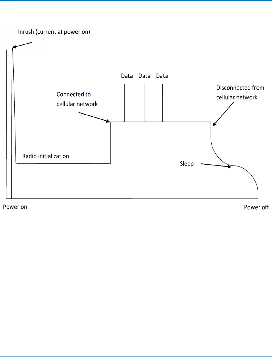
SPECIFICATIONS
Typical Power Flow
■Peak inrush current is a fast rising pulse at power start up on board supplies or modem cap charging. It is
influenced by the design and limits of the power supply providing power to the device.
■Radio initialization is a lower value steady current phase that occurs while the radio gets initialized and
ready to talk to the cell network.
■Once connected to the network, there is a steady idle current state.
■When data is transmitted to the network, power peaks from this idle state. Peak data values are influenced
by the distance from the towers and decided by the carrier network.
■Power starts dropping when the device is disconnected.
■After it is disconnected, power draw lowers if the device is told to enter sleep mode. Sleep mode keeps the
receiver active and the device periodically wakes up long enough to tell the network it is still available.
MultiConnectTM PCIe MTPCIE-H5/MTPCIE-BW Developer Guide 59
SPECIFICATIONS
Power Measurements
Multi-Tech Systems, Inc. recommends that you incorporate a 10% buffer into your power source when determining
product load.
MTPCIE-H5
Radio Cellular Call Box Average Measured Current TX Pulse (Avg) Total Inrush Charge
Protocol Connection No (Amps) at Maximum Power Amplitude Current Measured in
Data (Amps) (Amps) for GSM850 or Millicoulomb
Peak Current for HSDPA
3.3 Volts
GSM850 0.056 0.629 2.5 5.27
HSDPA 0.057 0.727 0.804 5.27
Note: Inrush Current:The input current during power up, or a reset.
MTPCIE-H5-V-BW
Radio Cellular Call Box Average Measured Current TX Pulse (Avg) Total Inrush Charge
Protocol Connection No (Amps) at Maximum Power Amplitude Current Measured in
Data (Amps) (Amps) for GSM850 or Millicoulomb
Peak Current for HSDPA
3.3 Volts
GSM850 0.062 1.058 2.9 2.51
HSDPA 0.062 0.970 1.052 2.51
Note: Inrush Current:The input current during power up, or a reset.
MTPCIE-BW
Voltage Inrush Current Idle Mode after MT100EOCG Max Power with Bluetooth and Wi-
(Amps) Boots Up (Amps) Fi in Broadcast Mode (Amps)
3.3 Volts 0.056 0.0064 0.326
Note: Inrush Current:The input current during power up, or a reset.
60 MultiConnectTM PCIe MTPCIE-H5/MTPCIE-BW Developer Guide
APPLICATION NOTES
Application Notes
RF Performances
RF performances are compliant with the ETSI recommendation 05.05 and 11.10. The module’s radio transceiver
meets the requirements of 3GPP Release 5 & 6. All values indicated are conducted.
Receiver Features for Cellular Devices
Category Description
GSM 850 Sensitivity < -109 dBm
E-GSM 900 Sensitivity < -106 dBm
DCS 1800 Sensitivity < -105 dBm
PCS 1900 Sensitivity < -105 dBm
UMTS Band I 2100 Sensitivity < -109 dBm
UMTS Band II 1900 Sensitivity < -108 dBm
UMTS Band V 850 Sensitivity < -110 dBm
UMTS Band VI 800 Sensitivity < -110 dBm
MultiConnectTM PCIe MTPCIE-H5/MTPCIE-BW Developer Guide 61

APPLICATION NOTES
Frequency Bands
Mode Freq. TX (MHz) Freq. RX (MHz) Channels TX-RX offset
GSM850 824.2- 848.8 869.2 - 893.8 128 - 251 45 MHz
EGSM900 890.0 - 914.8 935.0 - 959.8 0 - 124 45 MHz
880.2 - 889.8 925.2 - 934.8 975 - 1023 45 MHz
DCS1800 1710.2 - 1784.8 1805.2 - 1879.8 512 - 885 95 MHz
PCS1900 1850.2 - 1909.8 1930.2 - 1989.8 512 - 810 80 MHz
WCDMA850 (band V) 826.4 - 846.6 871.4 - 891.6 Tx: 4132 - 45 MHz
4233 Rx: 4357
- 4458
WCDMA900 (band 882.4 - 912.6 927.4 - 957.6 Tx: 2712 - 45 MHz
VIII) 2863 Rx: 2937
- 3088
WCDMA1700 (band 1710.4 - 1755.6 2112.4 - 2167.6 Tx: 1312 - 400MHz
IV) 1513 Rx: 9662
- 9938
WCDMA1900 (band II) 1852.4 - 1907.6 1932.4 - 1987.6 Tx: 9262 - 80MHz
9538 Rx: 9662
- 9938
WCDMA2100 (band I) 1922.4 - 1977.6 2112.4 - 2167.6 Tx: 9612 - 190MHz
9888 Rx:
10562 - 10838
62 MultiConnectTM PCIe MTPCIE-H5/MTPCIE-BW Developer Guide

INSTALLING DRIVERS FOR NON-UIP HSPA+ DEVICES
Installing Drivers for Non-UIP HSPA+ Devices
HSPA+ Device Driver Installation
Installing on Linux
The Linux OS includes a generic USB driver for modems supporting CDC/ACM.
Multi-Tech tested the following Linux operating systems and all used port ttyACM0. If your system has another
device using this port, your port numbers may be different.
■Ubuntu
■Debian
■Centos
■Ubuntu 13.04
■Debian 6.0.6
■Fedora 15
■openSUSE 11.4
■CentOS 6.0
To install the device on any Linux Kernel with CDC/ACM support, connect USB cable from the device to a USB port
on your computer. For most recent Linux distributions, there are no drivers to install.
If the operating system recognizes the modem, seven devices are created (assuming no other ACM values have
been assigned):
■/dev/ttyACM0
■/dev/ttyACM1
■/dev/ttyACM2
■/dev/ttyACM3
■/dev/ttyACM4
■/dev/ttyACM5
■/dev/ttyACM6
Only the following devices can be used for AT commands:
■/dev/ttyACM0 (data port for PPP connections and AT commands)
■/dev/ttyACM3 (generic port for AT commands)
Troubleshooting Linux
If Linux does not create devices, check for the kernel module:
# lsmod | grep cdc_acm
If entries aren't found, load the kernel module with root privileges:
# modprobe cdc-acm
MultiConnectTM PCIe MTPCIE-H5/MTPCIE-BW Developer Guide 63

INSTALLING DRIVERS FOR NON-UIP HSPA+ DEVICES
If this returns an error response, such as # FATAL: Module cdc-acm not found, the kernel module is not on your
system. You will need to build the driver.
Building a Linux Driver
If your system is missing the Linux driver:
1. Retrieve the appropriate kernel source code version for your system. This should be in your OS
distribution package. Unpack it.
2. In its root directory type: # make menuconfig
3. Configure the kernel according to your system configuration,
4. Browse to menu Device Driver > USB Support and select USB Modem (CDC ACM) support.
5. To start the build once configured, type # make
The kernel module cdc-acm.ko is in the directory drivers/usb/class. If the kernel was built previously, compile the
module by typing:
# make M=drivers/usb/class
To load the module use modprobe or insmod.
Windows Release Notes
We tested h5-u-windriver_8.00.04.zip ev3-u_windriver_8.00.04.zip driver on the following Windows operating
systems.
■Windows 8 x86 and x64, Windows 7 x86 and x64, Vista x86 and x64, XP x86 and x64, Windows Server
2012, Windows Server 2008 x86 and x64, and Windows Server 2003 x86
■Drivers install correctly, but may require .NET Framework version 3.5 or older.
■After installing the driver for this device, the device may not be available when Windows comes out of a
sleep/hibernate state. To correct this issue, unplug the device from the USB port and then plug it back in
to the same port.
■Windows Server 2003 x64
■Not supported with version 8.00.04.
Downloading the Windows USB Driver
If you haven't downloaded the driver:
1. Go to the Multi-Tech Support page, www.multitech.com/support.go and select your product from the
Product Families drop down list.
2. Click Drivers.
3. Select h5-u_windriver_8.00.04.zip and Save the driver to your computer.
4. Extract the files to your computer.
Windows Notes
Installing on USB Host Powered Devices
When you connect a USB host powered device to a computer through a USB cable, the Windows Add New
Hardware Wizard may display Cannot Install this Hardware. If this occurs, click Finish. Windows detects additional
devices and prompts you to install them.
64 MultiConnectTM PCIe MTPCIE-H5/MTPCIE-BW Developer Guide

INSTALLING DRIVERS FOR NON-UIP HSPA+ DEVICES
Installing on Non-USB Powered Devices
Turn on the device and wait 15 seconds before connecting the USB cable. If you connect the USB cable before
supplying power to the device, the Windows Add New Hardware Wizard may appear and show Cannot Install this
Hardware. If this occurs, click Finish. Windows detects additional devices and prompts you to install the additional
devices. If Windows does not detect new device, unplug the USB cable, turn the device off and on, wait 15
seconds, insert the USB cable, and install devices when prompted.
Installing on Windows 8, 7 or Vista
This process installs multiple drivers and ports.
Note: If you previously installed USB drivers for this device, uninstall them before installing or re-installing this
driver. Uninstall all existing drivers for this device. Refer to Uninstall Windows Drivers for details.
Before you connect the device (disconnect the device if you connected it):
CAUTION: If you connected the device before installing the drivers, Windows may install drivers automatically.
Your device may not operate correctly with these drivers. Uninstall the drivers before proceeding. See Remove
Microsoft Installed Drivers for details.
1. Go to the location where you extracted the driver and open the H5-USB\Driver folder.
2. Right-click on TelitUSBInstaller_In_U8.00.04.exe and select Run as Administrator.
3. Click Yes or Allow to allow the installer to make changes to your computer.
4. Click Next and follow the instructions in the installation wizard.
5. Click the Install option when prompted, for example, Install this driver software anyway.
6. Click Finish.
7. Connect USB cable from the device to a USB port on your computer. Windows indicates when the device
is ready to use.
8. Signal strength LEDs require a device reboot after installing software. Disconnect the device from the
computer's USB port for a few seconds and reconnect the device to the same USB port.
MultiConnectTM PCIe MTPCIE-H5/MTPCIE-BW Developer Guide 65
INSTALLING DRIVERS FOR NON-UIP HSPA+ DEVICES
Installing on Windows XP
This process installs four drivers.
Note: If you previously installed USB drivers for this device, uninstall them before installing or re-installing this
driver. Uninstall all existing drivers for this device. Refer to Uninstall Windows Drivers for details.
Before you connect the device (disconnect the device if you connected it):
1. Go to the location where you extracted the driver and open the H5-USB\Driver folder.
2. Right-click on TelitUSBInstaller_In_U8.00.04.exe and select Run.
3. Click Next and follow the instructions in the installation wizard.
4. Click Continue Anyway each time this screen appears.
5. Click Finish.
6. Connect USB cable from the device to a USB port on your computer. After it detects the hardware,
Windows opens the New Hardware Wizard.
7. Select No, not this time and click Next.
8. Select Install the software automatically (Recommended) and click Next.
9. Select Finish.
10. Repeat Steps 7-9 for each additional New Hardware Wizard. Windows indicates when the device is ready
to use.
11. Signal strength LEDs require a device reboot after installing software. Disconnect the device from the
computer's USB port for a few seconds and reconnect the device to the same USB port.
66 MultiConnectTM PCIe MTPCIE-H5/MTPCIE-BW Developer Guide

INSTALLING DRIVERS FOR NON-UIP HSPA+ DEVICES
Uninstalling Windows Drivers
Note: Disconnect the device before uninstalling drivers.
Windows 8
To uninstall drivers from Windows 8:
1. Open Windows Programs and Features.
2. Uninstall Windows Driver Package – Intel Mobile Communications (flashusb) USB.
3. Uninstall all Telit modems, ports, and USB drivers.
Windows 7 or Vista
To uninstall drivers from Windows 7 or Vista:
1. Open Programs and Features from the Windows Control Panel.
2. Uninstall the Windows Driver Package – Telit Wireless Solutions (telitusbser) Modem.
3. Uninstall all Telit modems, ports, and USB.
Windows XP
To uninstall drivers from Windows XP:
1. Open the Control Panel and go to Add or Remove Programs.
2. Uninstall Windows Driver Package – Telit Wireless Solutions (telitusbser) Modem.
3. Uninstall all other Telit modems, Ports and USB.
Remove Microsoft Installed Drivers
If using Windows 7 and connect the device before installing drivers, Windows Update automatically installs drivers.
Your device may not operate correctly with these drivers. To remove these drivers:
1. With the device plugged in, open the Device Manager.
MultiConnectTM PCIe MTPCIE-H5/MTPCIE-BW Developer Guide 67
INSTALLING DRIVERS FOR NON-UIP HSPA+ DEVICES
2. Right-click on the Telit Mobile Modem and select Uninstall.
3. Select Delete the driver software for this device and click OK.
4. Repeat the removal steps to uninstall each Telit port and the Telit Universal Serial Bus Control.
Developer Note
By default each time an H5 device with a different IMEI value is connected using this USB driver, the operating
system will not require searching for the drivers again and uses the same ports created in a previous installation.
To prevent this, use the utility included with the driver download to manage port creation as follows.
To enable USB IMEI identification, where the operating system creates a new set of ports with different COM
enumeration for each H5 device with a different IMEI value:
1. Uninstall the driver if already installed.
2. Double-click H5_enable_USB_IMEI_indentification.reg in the folder where you extracted the driver files.
3. Install the driver as normal.
To disable USB IMEI identification (driver default setting):
1. Uninstall the driver if already installed.
2. Double-click H5_disable_USB_IMEI_indentification.reg in the folder where you extracted the driver files.
3. Install the driver as normal.
68 MultiConnectTM PCIe MTPCIE-H5/MTPCIE-BW Developer Guide

USING LINUX WITH H5 DEVICES
Using Linux with H5 Devices
Shell Commands
Testing Serial Ports
To test the serial ports created by the driver, type in a shell:
# cat /dev/ttyACM0 &
# echo –en "ATE0\r" > /dev/ttyACM03
# echo –en "AT\r" > /dev/ttyACM0
Note: Sending ATE0 is required, to avoid issues in the terminal output. It prevents the sending/receiving
spurious characters to/from the modem when used with the Linux commands “echo” and “cat”
You can perform the same test using the other interface (ttyACM1 ttyACM3).
Create a PPP Connection
Most recent Linux distributions have GUI tools for creating PPP connections; the following instructions are for
creating a PPP connection through command line interface.
PPP support must be compiled into the kernel; pppd and chat programs are also required.
pppd needs two scripts: the first script performs the environment setting and calls the second script, which is used
by the chat program. For creating a PPP connection type:
# pppd file /etc/pppd_script &
Example
# Debug info from pppd
debug
#kdebug 4
# Most phones don't reply to LCP echos
lcp-echo-failure 3
lcp-echo-interval 3
# Keep pppd attached to the terminal
# Comment this to get daemon mode pppd
nodetach
# The chat script (be sure to edit that file, too!)
connect "/usr/sbin/chat -v -f /etc/chatscripts/hsdpa_connect"
# Serial Device to which the modem is connected
/dev/ttyACM3
# Serial port line speed
115200
dump
# The phone is not required to authenticate
#noauth
user <insert here the correct username for authentication>
name <insert here the name of the connection>
password <insert here the correct password for authentication>
MultiConnectTM PCIe MTPCIE-H5/MTPCIE-BW Developer Guide 69

USING LINUX WITH H5 DEVICES
# If you want to use the HSDPA link as your gateway
defaultroute
# pppd must not propose any IP address to the peer
#noipdefault
ipcp-accept-local
ipcp-accept-remote
# Keep modem up even if connection fails
#persist
# Hardware flow control
crtscts
# Ask the peer for up to 2 DNS server addresses
usepeerdns
# No ppp compression
novj
nobsdcomp
novjccomp
nopcomp
noaccomp
# For sanity, keep a lock on the serial line
lock
# Show password in debug messages
show-password
This script calls the option connect using the script hsdpa_connect, for example: #!/bin/sh
# Connection to the network
'' AT+CGDCONT=1,"IP","<insert here the correct APN provided by
your network operator>"
# Dial the number.
OK ATD*99***1#
# The modem is waiting for the following answer
CONNECT ''
After launching a PPP connection is possible to use ftp protocol or other utilities that allow the access to the
Internet.
C Programming
The following topics show all the functions that can be used from C source code to perform read/write operations
on the serial devices.
open()
The open() function shall establish the connection between a file and a file descriptor. The file descriptor is used by
other I/O functions to refer to that file.
Header File
fcntl.h
Prototype:
int open(const char *pathname, int flags)
Parameters:
70 MultiConnectTM PCIe MTPCIE-H5/MTPCIE-BW Developer Guide

USING LINUX WITH H5 DEVICES
pathname – file name with its own path.
flags – is an int specifying file opening mode: is one of O_RDONLY, O_WRONLY or O_RDWR which request opening
the file read-only, write-only or read/write, respectively.
Returns:
The new file descriptor fildes if successful, -1 otherwise.
Example
Open the /dev/ttyACM0.
int fd; // file descriptor for the /dev/ttyACM0 entry
if((fd = open("/dev/ttyACM0", O_RDONLY) < 0)
{
/* Error Management Routine */
} else {
/* ttyACM0 Device Opened */
}
read()
The read() function reads nbyte bytes from the file associated with the open file descriptor, fildes, and copies them
in the buffer that is pointed to by buf.
Header File
unistd.h
Prototype:
ssize_t read(int fildes, void *buf, size_t nbyte)
Parameters:
fildes - file descriptor
buf - destination buffer pointer
nbyte - number of bytes that read() attempts to read
Returns:
The number of bytes actually read if the operation is completed successfully, otherwise it is -1.
Example
Read sizeof(read_buff) bytes from the file associated with fd and stores them into read_buff.
char read_buff[BUFF_LEN];
if(read(fd, read_buff, sizeof(read_buff)) < 0)
{
/* Error Management Routine */
} else {
/* Value Read */
}
MultiConnectTM PCIe MTPCIE-H5/MTPCIE-BW Developer Guide 71

USING LINUX WITH H5 DEVICES
write()
The write() function writes nbyte bytes from the buffer that are pointed by buf to the file associated with the open
file descriptor. fildes.
Header File
unistd.h
Prototype:
ssize_t write(int fildes, const void *buf, size_t nbyte)
Parameters:
fildes – file descriptor
buf – destination buffer pointer
nbyte – number of bytes that write() attempts to write
Returns:
The number of bytes actually written if the operation is completed successfully, otherwise it is -1.
Example
Write strlen(value_to_be_written) bytes from the buffer pointed by value_to_be_written to the file
associated with the open file descriptor, fd.
char value_to_be_written[] = “dummy_write”;
if (write(fd, value_to_be_written, strlen(value_to_be_written)) < 0)
{
/* Error Management Routine */
} else {
/* Value Written */
}
close()
The close() function shall deallocate the file descriptor indicated by fildes. To deallocate means to make the file
descriptor available for return by subsequent calls to open() or other functions that allocate file descriptors.
Header File
unistd.h
Prototype:
int close(int fildes);
Parameters:
fildes - file descriptor
Returns:
0 if successful, otherwise it is -1.
72 MultiConnectTM PCIe MTPCIE-H5/MTPCIE-BW Developer Guide

USING LINUX WITH H5 DEVICES
Example
Close the ttyACMx file.
if(close(fd) < 0)
{
/* Error Management Routine */
} else {
/* File Closed */
}
Test Program()
The following simple C program is useful to test the modem issuing an AT command. The program opens the
/dev/ttyACM0 interface and calls the write() and the read() function to send an AT command and receive the
subsequent output.
#include <stdio.h> /* Standard input/output definitions */
#include <string.h> /* String function definitions */
#include <unistd.h> /* UNIX standard function definitions */
#include <fcntl.h> /* File control definitions */
#include <errno.h> /* Error number definitions */
#include <termios.h> /* POSIX terminal control definitions */
#define USB "/dev/ttyACM0"
#define BUFSIZE 1000
#define BAUDRATE B115200
int open_port(char *port)
{
struct termios options;
int fd;
fd = open(port, O_RDWR | O_NOCTTY | O_NDELAY);
if (fd == -1)
{
printf("open_port: Unable to open the port - ");
}
else
{
printf ( "Port %s with file descriptor=%i",port, fd);
fcntl(fd, F_SETFL, FNDELAY);
tcgetattr( fd, &options );
cfsetispeed( &options, BAUDRATE );
cfsetospeed( &options, BAUDRATE );
options.c_cflag |= ( CLOCAL | CREAD);
options.c_cflag &= ~(CSIZE | PARENB | CSTOPB | CSIZE);
options.c_cflag |= CS8;
options.c_cflag &= ~CRTSCTS;
options.c_lflag &= ~(ICANON | ECHO | ECHOE | ISIG);
options.c_iflag &= ~(IXON | IXOFF | IXANY | ICRNL | INLCR |
IGNCR);
options.c_oflag &= ~OPOST;
if ( tcsetattr( fd, TCSANOW, &options ) == -1 )
printf ("Error with tcsetattr = %s\n", strerror ( errno )
);
MultiConnectTM PCIe MTPCIE-H5/MTPCIE-BW Developer Guide 73

USING LINUX WITH H5 DEVICES
else
printf ( "%s\n", "succeed" );
}
return (fd);
}
int main()
{
int serialFD = open_port(USB);
char buf[BUFSIZE];
memset(buf,0,BUFSIZE);
write(serialFD, "AT\r" , strlen("AT\r"));
sleep(1);
read( serialFD, buf, BUFSIZE );
printf("The string is: %s\n", buf);
close(serialFD);
return 0;
}
The sleep instruction is required because the modem response after issuing the AT command is not immediate, so
you need to wait a bit before reading. There are more efficient ways to do this, for example, you can put the read
call in a while loop and exit when the read buffer contains a certain string.
74 MultiConnectTM PCIe MTPCIE-H5/MTPCIE-BW Developer Guide

INDEX
Index
AESD ................................................................................15
European Community Directives ..................................36
account activation.........................................................47
activation
cellular devices.........................................................47 F
antenna .........................................................................42 FCC
cable....................................................................43 45 grant notes...............................................................45
cellular devices.........................................................42 frequency bands ...........................................................62
GPS...........................................................................44
Wi-Fi RF....................................................................44
assembly diagram .........................................................18 G
GPS
Bantenna....................................................................44
ground plane.................................................................14
Bluetooth ......................................................................47
build options ..............................................................6 47
H
Chandling precautions due to ESD..................................15
hazardous substances ...................................................37
cable.........................................................................43 45 host labeling..................................................................45
CAD drawing.............................................................49 50 HSPA+............................................................................34
CE mark .........................................................................36 HSPA+21........................................................................47
Chinese hazardous substances
Chinese version........................................................41
English version .........................................................40 I
C programming IMEI ...............................................................................34
close .........................................................................72 install
open .........................................................................70 SIM card ...................................................................31
read..........................................................................71 installing
test program ............................................................73 device on board .......................................................31
write.........................................................................72
J
D
jumpers .........................................................................30
developer board............................................................16
device
maintenance ............................................................33 L
dialing restrictions.........................................................37
drawing ....................................................................49 50 labeling
host ..........................................................................45
labels .............................................................................34
ELinux
building driver..........................................................64
electrical C programming ........................................................70
characteristics..........................................................53 driver........................................................................47
electromagnetic interference .......................................14 install........................................................................63
electrostatic discharge..................................................15 PPP connection ........................................................69
EMI ................................................................................14
MultiConnectTM PCIe MTPCIE-H5/MTPCIE-BW Developer Guide 75

INDEX
shell commands .......................................................69 T
troubleshoot driver..................................................63 transmitter features......................................................61
MU
maintenance .................................................................33 uninstall.........................................................................67
mechanical drawing .................................................49 50 USB...........................................................................13 67
design consideration................................................15
driver download.......................................................64
N
notes ........................................................................64
noise suppression..........................................................14 USB driver
install..............................................................63 65 66
uninstall ...................................................................67
Puser responsibility.........................................................33
PC board layout.............................................................14
pinout............................................................................53
V
USB...........................................................................13
pinout table.....................................................................8 vehicle safety ................................................................32
standard...................................................................11 Vista .........................................................................65 67
power draw...................................................................60
PTCRB ............................................................................34
W
Wi-Fi ..............................................................................47
R
Wi-Fi RF specifications ..................................................44
radio frequency interference........................................32 Windows
receiver features...........................................................61 release notes............................................................64
RoHS..............................................................................37 USB driver download ...............................................64
USB driver release notes..........................................64
Windows 7 ...............................................................65 67
SWindows 8 ....................................................................65
safety uninstall ...................................................................67
RF interference ........................................................32 Windows XP .............................................................66 67
vehicle......................................................................32
safety standards............................................................14
X
SIM card ........................................................................31
specifications.................................................................51 XP ..................................................................................66
76 MultiConnectTM PCIe MTPCIE-H5/MTPCIE-BW Developer Guide