Multitone Electronics PLC RPE673 Multitone RPE673 Radio Paging Transcoder User Manual Prelim
Multitone Electronics PLC Multitone RPE673 Radio Paging Transcoder Prelim
UserManual.wiki
>
Multitone Electronics PLC
>
RPE673 User Manual
>
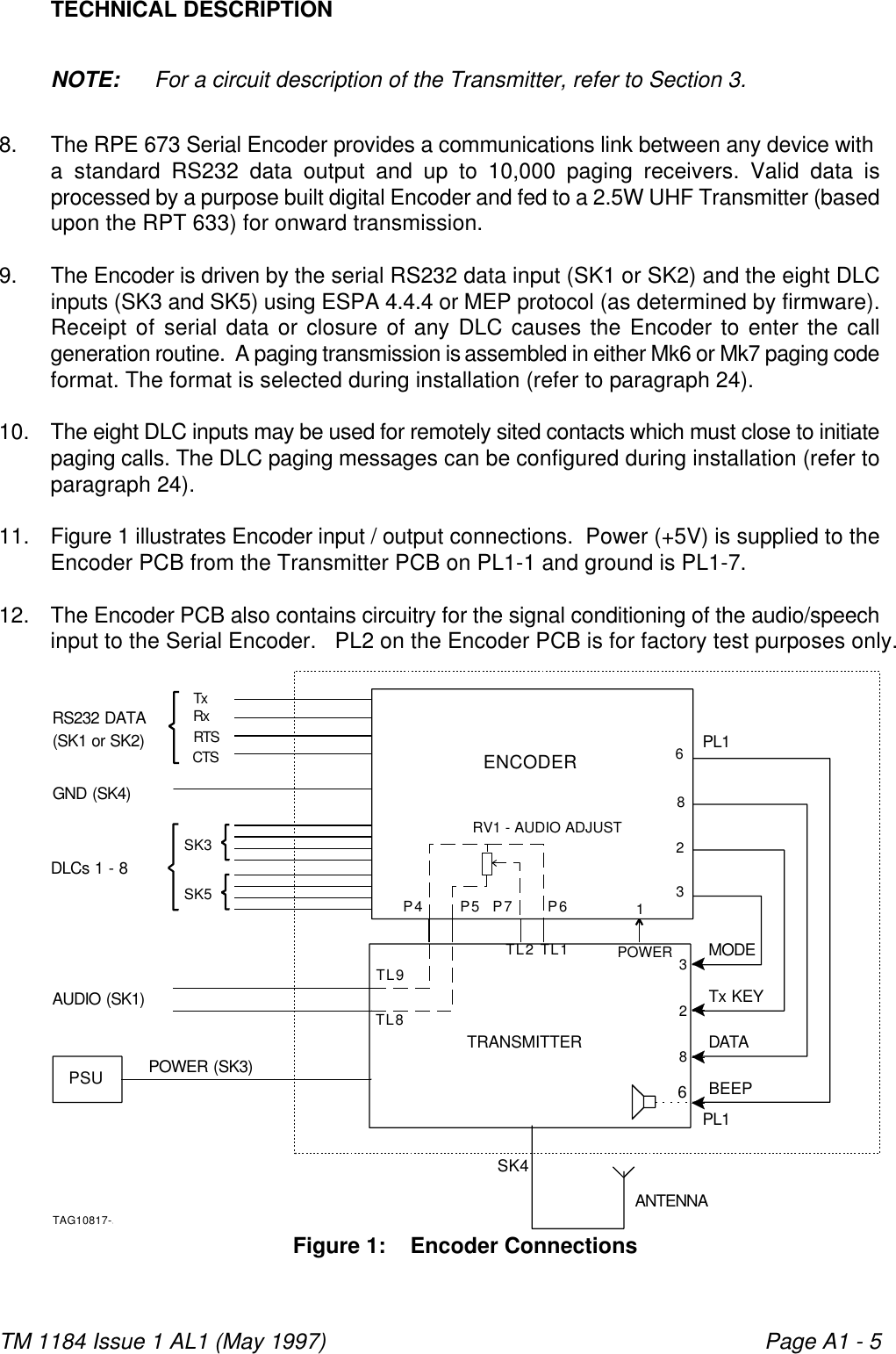
Users manual
Contents
1.
User information
2.
Users manual
Users manual
Navigation menu
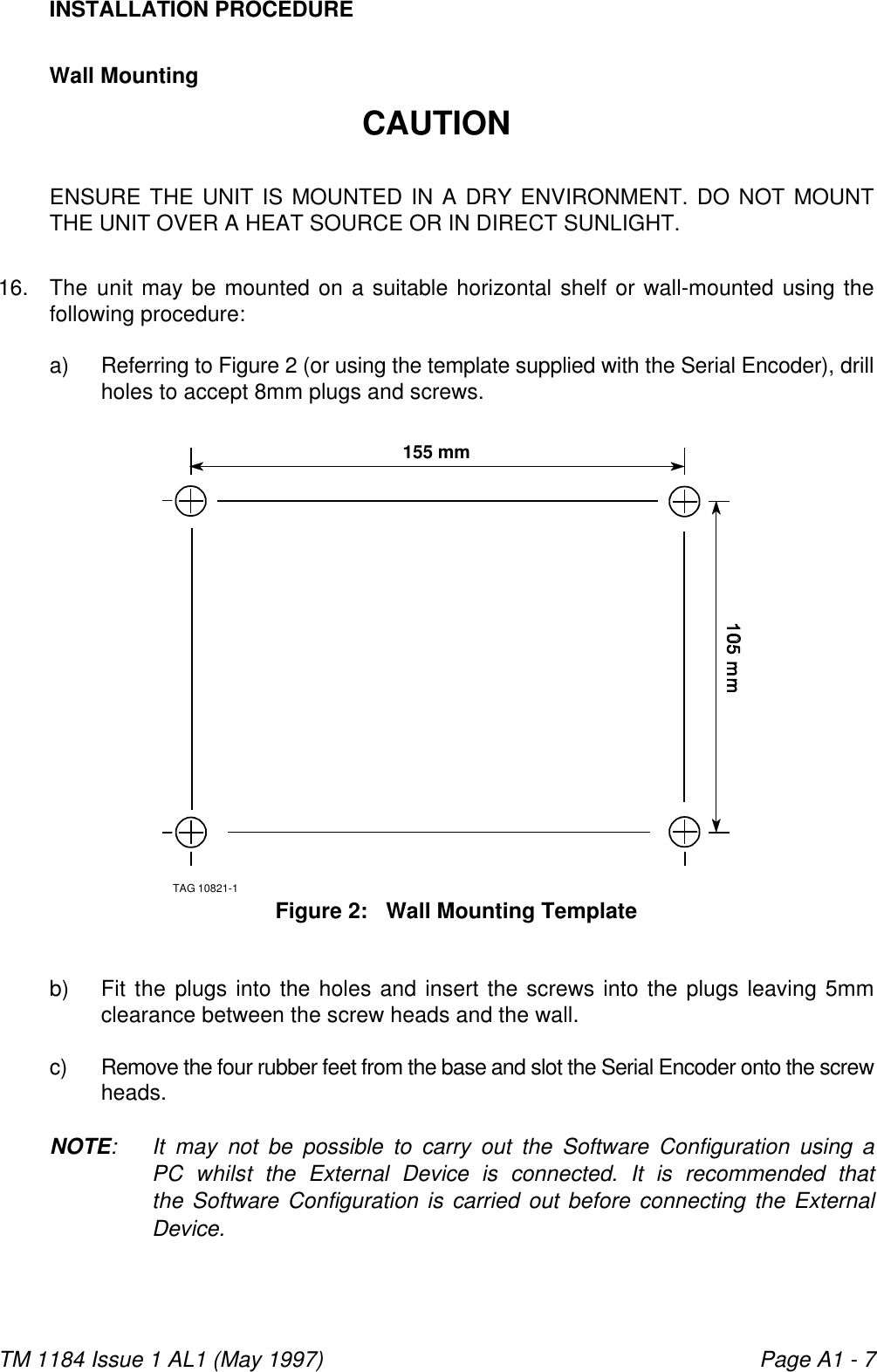
Upload a User Manual
Namespaces
Wiki Guide
HTML
PDF
Info
Views
User Manual
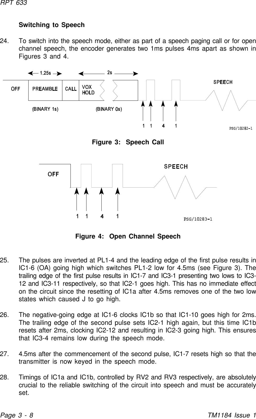
Discussion / Help
Navigation


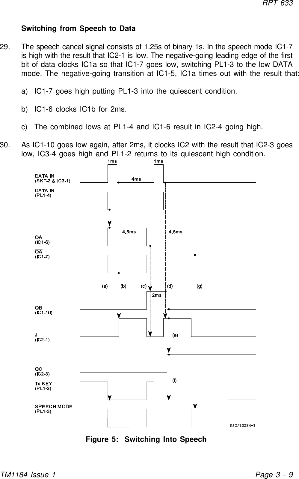
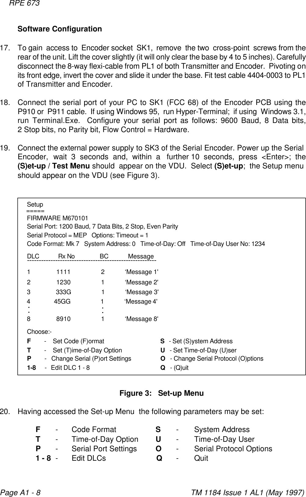
![TM 1184 Issue 1 AL1 (May 1997) Page A1 - 921. Definitions for each parameter are given in paragraph 24.22. Once a setting has been selected, the following message will be displayed:‘....Writing to Eeprom - please wait.....Done’and the Set-up screen will again be displayed. 23. For Serial Port Settings however, parameters are not written to the Eeprom until‘W’ (Write to Eeprom) is selected from the Serial Port Set-up Menu.Parameter Definitions24. The Parameter Definitions are as follows:DLC Each DLC has a configurable Receiver Number (Rx No), Beep Code (BC) andConfiguration Message.a) Rx No Four digit code in the range 0000 - 9999. The Rx No will beautomatically prefixed with the System Address to form the RIC.Group calls may be initiated in order to call a group of pagingreceivers within a specified range of addresses by inserting thewildcard character ‘G’ into the Rx No.If one wildcard character is included as the least significant digitthen a group of 10 receivers will be called, eg: ’333G willcall receivers ’3330 to ’3339 (where ’ = SystemAddress).If two wildcard characters are included as the two least significantdigits then a group of 100 receivers will be called, eg: ’45GGwill call receivers ’4500 to ’4599 (where ’ = System Address). b) Beep Single digit in the range 1 - 8Codec) Message Mk6: Maximum length of 10 characters in the range 0 - 9,(hyphen) and <Space>. Mk7: Maximum length of 60 characters in the standard ASCIIcharacter set ie,<Space> (Hex 20) through to ‘~’ (Hex7E).Serial Port These parameters are for the V24/RS232 port and are set to match theSettings External Device to which the Serial Encoder is connected. The selections are selfexplanatory however, once the settings have been made, they must bewritten to the Eeprom by entering ‘W’ ([W]rite changes to Eeprom).NOTE: During set-up and test, the Serial Encoder communicates using a fixedset of parameters (9600 Baud, 8 Data Bits, 2 Stop Bits, No Parity Bit).The above Serial Port Settings only take effect during normal operation.](https://usermanual.wiki/Multitone-Electronics-PLC/RPE673.Users-manual/User-Guide-234688-Page-55.png)