Multitone Electronics PLC RPE673 Multitone RPE673 Radio Paging Transcoder User Manual Prelim
Multitone Electronics PLC Multitone RPE673 Radio Paging Transcoder Prelim
Contents
- 1. User information
- 2. Users manual
Users manual

RPT 633
TM1184 Issue 1 AL1 (May 1997) Page (i)
TECHNICAL MANUAL
for
UHF TRANSMITTER
MODEL RPT 633
and
UHF SERIAL ENCODER
MODEL RPE 673
Printed and published in England

RPT 633
Page (ii) TM1184 Issue 1 AL1 (May 1997)
©Multitone Electronics plc 1997
COMPANY LIABILITY
The information in this manual has been carefully compiled and checked for technical
accuracy. Multitone Electronics plc accept no liability for inaccuracies or errors. In line with
the company policy of technical advancement, the information within this document may be
changed. The user should ensure that the correct issue of the document is used.
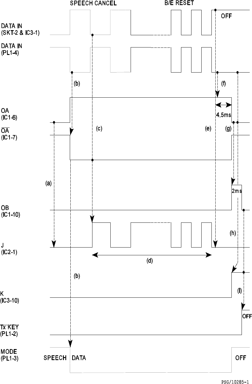
Comments or correspondence regarding this manual should be addressed to:
Multitone Electronics plc
Technical Publications
Multitone House
Beggarwood Lane
Kempshott Hill
Basingstoke
Hampshire
RG23 7LL
England
ISSUE DATE
1April 1994
RPT 633
TM1184 Issue 1 AL1 (May 1997) Page (iii)
CONTENTS
Page (i) Title Page
Page (ii) Company Liability
Page (iii) Contents
Page (iv) Effective Page List
Page (v) Safety Summary
Warning
Page (vi) Cautions
Section 1Introduction and Specification
Section 2Operating Instructions
Section 3Technical Description
Section 4Installation and Commissioning
Section 5Servicing
Section 6Spare Parts List
Section 7Diagrams
Appendix 1UHF Serial Encoder Model RPE 673
RPT 633
Page (iv) TM1184 Issue 1 AL1 (May 1997)
EFFECTIVE PAGE LIST
Page No. Issue Page No. Issue Page No. Issue
(i) 1 AL1 4-5 17-11 1
(ii) 1 AL1 4-6 1
(iii) 1 AL1 5-1 1A1-1 1 AL1
(iv) 1 AL1 5-2 1A1-2 1 AL1
(v) 15-3 1A1-3 1 AL1
(vi) 15-4 1A1-4 1 AL1
1-1 1 AL1 5-5 1A1-5 1 AL1
1-2 15-6 1A1-6 1 AL1
1-3 15-7 1A1-7 1 AL1
1-4 15-8 1A1-8 1 AL1
2-1 15-9 1A1-9 1 AL1
2-2 15-10 1A1-10 1 AL1
3-1 16-1 1A1-11 1 AL1
3-2 16-2 1A1-12 1 AL1
3-3 16-3 1A1-13 1 AL1
3-4 16-4 1A1-14 1 AL1
3-5 16-5 1A1-15 1 AL1
3-6 16-6 1A1-16 1 AL1
3-7 16-7 1A1-17 1 AL1
3-8 16-8 1A1-18 1 AL1
3-9 17-1 1A1-19 1 AL1
3-10 17-2 1A1-20 1 AL1
4-1 17-3/4 1A1-21 1 AL1
4-2 17-5/6 1A1-22 1 AL1
4-3 17-7/8 1A1-23 1 AL1
4-4 17-9/10 1A1-24 1 AL1

RPT 633
TM 1184 Issue 1(v)
GREAT CARE MUST BE TAKEN TO AVOID BREAKING OPEN THE
ENCAPSULATION OF TR10 ON THE TRANSMITTER BOARD WHEN REPAIR OR
COMPONENT REPLACEMENT IS BEING CARRIED OUT, AS THIS COMPONENT
CONTAINS TOXIC BERYLLIUM OXIDE.
SAFETY SUMMARY
The following information applies to both operating and servicing personnel. General
Warnings and Cautions will be found throughout the manual where they apply.
WARNING statements identify conditions or practices that could result in personal injury or
loss of life.
CAUTION statements identify conditions or practices that could result in equipment damage.
WARNING
RPT 633
TM 1184 Issue 1(vi)
CAUTIONS
DO NOT MOUNT OVER A HEATER OR RADIATOR, OR IN DIRECT SUNLIGHT AND
ENSURE A DRY ENVIRONMENT.
STATIC SENSITIVE DEVICES ARE USED WITHIN THIS EQUIPMENT. CARE MUST BE
TAKEN TO ENSURE DAMAGE TO THESE DEVICES IS NOT CAUSED BY HIGH LEVELS
OF STATIC ELECTRICITY. SPARE BOARDS OR COMPONENTS SHOULD BE STORED
IN ANTI-STATIC PACKAGING WHEN NOT INSTALLED IN THE EQUIPMENT.
RPT 633
TM1184 Issue 1 AL1 (May 1997) Page 1 - 1
SECTION 1
INTRODUCTION AND SPECIFICATION
CONTENTS:
1. INTRODUCTION
2. ROLE OF THE TRANSMITTER
4. PHYSICAL CONSTRUCTION
SPECIFICATIONS
5. Transmitter
6. Connectors
7. Physical Characteristics
8. Operational Enviroment
9. Power Supply
10. CRYSTAL FREQUENCY CALCULATION
_______________________
INTRODUCTION
1. Sections 1 to 7 of this manual outline the installation and operation of the Radio
Paging Transmitter model RPT 633. Appendix 1 details the Serial Encoder model RPE
673 and provides appropriate cross references to the main part of this manual
(Sections 1 to 7) where functionality is common.
ROLE OF THE TRANSMITTER
2. The transmitter is designed for operation with the RPE 340-series of telephone coupled
encoders, or from the encoder output of the Access 3000, which together provide radio
coverage with speech for smaller sites. The RPT 633 operates in the UHF band
(420MHz to 470MHz), divided into three sub-bands, and has an output of 2.5 Watts.
3. Digital control reduces the wiring between the encoder and transmitter to a single pair
for tone and display systems. A four wire connection is required for speech systems.
RPT 633
TM 1184 Issue 1Page 1 - 2
PHYSICAL CONSTRUCTION
4. The transmitter consists of two boards, a transmitter board mounted in the base
assembly and a VOX keying module mounted in the cover assembly.
SPECIFICATIONS
Transmitter
5. The following describes the performance and physical characteristics of the RPT 633
UHF transmitter:
a) Frequency Range: 420MHz to 470MHz
b) Frequency Bands: Band 1420MHz to 424.99MHz
Band 2425MHz to 446.99MHz
Band 3447MHz to 470MHz
c) Channel Spacing: Factory set to 10kHz, 12.5kHz, 20kHz
or 25kHz
d) Frequency Stability (normal): ±5ppm from -10EC to +55EC
(high stability): ±1.5ppm from -10EC to +55EC
±2ppm from -25EC to +55EC
±2.5ppm from -30EC to +60EC
e) Output Power: 2.5W ±1dB
f) Duty Cycle: 50% (Max transmit time 2.5 minutes)
g) Nominal Load Impedance: 50 Ohms
h) VSWR Protection: Protection against short term removal
of antenna (maximum of five calls with
antenna disconnected).
Connectors
6. The following connectors are mounted on the transmitter board:
a) PSU - SK3: 2.1mm jack socket
b) Digital - SK2: 2-way modular keyed connector
c) Analogue - SK1: 2-way modular keyed connector
d) RF - SK4: TNC socket

RPT 633
TM 1184 Issue 1Page 1 - 3
Physical Characteristics
7. The dimensions and weight of the transmitter are as follows:
a) Overall Dimensions: Width 235mm (9.5in.)
Depth 210mm (8.3in.)
Height 90mm (3.6in.)
b) Weight (Excluding PSU): 1.2kg (2.65lbs.)
Operational Environment
8. The environmental characteristics of the transmitter are as follows:
a) Temperature Range: Operational -10EC to +50EC
b) Humidity: 0-90% RH (non-condensing)
c) Altitude: Up to 2000 metres
Power Supply
9. 17V 0.8A DC Nominal supplies from Multitone Power Supplies:
0301-0605 240V (UK)
0301-0606 220V (EURO)
0301-0607 110V (US)
CRYSTAL FREQUENCY CALCULATION
10. To calculate the carrier crystal frequency the following formula should be used:
Crystal Frequency = Operating Frequency
A
Where A = 56 for Band 3
or A = 48 for Bands 1 and 2
RPT 633
TM 1184 Issue 1Page 1 - 4
INTENTIONALLY BLANK
RPT 633
TM1184 Issue 1Page 2 - 1
SECTION 2
OPERATING INSTRUCTIONS
The transmitter is fully automatic in use and operation is limited to switching on the mains
supply.
RPT 633
Page 2 - 2TM1184 Issue 1
INTENTIONALLY BLANK
RPT 633
TM1184 Issue 1Page 3 - 1
SECTION 3
TECHNICAL DESCRIPTION
CONTENTS:
1. INTRODUCTION
TRANSMITTER
2. Power Supplies
3. Mode Select Circuit
5. Audio Input
6. Data Input
7. Crystal Oscillator
8. High Stability Version
9. Voltage Controlled Oscillator (VCO)
10. Phase Locked Loop (PLL)
11. Transmitter Keying
13. Frequency Multiplier
14. Band Pass Filter
15. Driver Stages
16. Output Amplifier
VOX KEYING MODULE
17. General
18. Analogue Path
19. Data Mode
20. Decoding
OPERATION
21. General
22. Power Up
23. Data Path
24. Switching to Speech
29. Switching from Speech to Data
TABLES Page
1. VOX Keying and Mode Signals 3-7
PLL
CIRCUIT RF
CIRCUIT
DATA
CIRCUIT
SPEECH
CIRCUIT
VOX
KEYING
MODULE
ANALOGUE INPUT
DATA
MODE
Tx KEY
PSG/10280-1
DIGITAL
INPUT
RPT 633
Page 3 - 2TM1184 Issue 1
CONTENTS: (Continued)
FIGURES Page
1. Block Diagram 3-2
2. Module Interconnection Diagram 3-6
3. Speech Call 3-8
4. Open Channel Speech 3-8
5. Switching Into Speech 3-9
6. Switching From Speech 3-10
_______________________
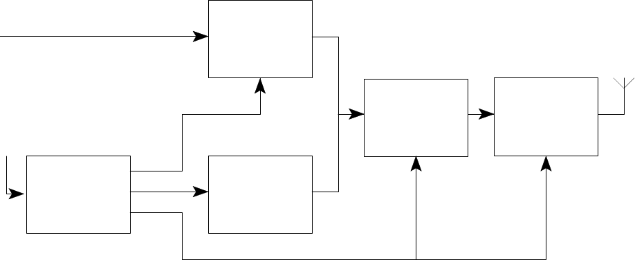
INTRODUCTION
1. The RPT 633 Transmitter accepts analogue or digital information which is
modulated onto an UHF signal. The transmitter output frequency is produced by
doubling the frequency of a voltage controlled oscillator (VCO). The VCO is locked
to a reference crystal oscillator which is frequency modulated by either the Data or
Audio input signals. A basic block diagram is shown at Figure 1.
Figure 1: Block Diagram
TRANSMITTER
Power Supplies
2. A nominal 17V DC power supply is fed into the board at SK3 where it is filtered
by L14, L15, L16, C67 and C68. Fixed voltage regulators IC3 and IC4 provide 12V
for the transmitter circuit and output transistor respectively, while regulator IC5
produces 5V for the transmitter and VOX Keying module. Integrated circuit IC2
produces 8.2V for the VCO and buffer amplifiers and IC11 acts as a voltage
converter to produce -11V from a 12V input.
RPT 633
TM1184 Issue 1Page 3 - 3
Mode Select Circuit
3. With the mode input at 5V the Speech mode is selected. The output of IC6d is low,
inhibiting the passage of Data by shorting the data path to 0V via D11 and
enabling the passage of Audio by forward biasing D9. Variable resistor RV3
together with R102, R103, R108 and R116 hold the output of IC12d at
approximately 0V, which in turn sets the voltage on varactor diode D8 to give the
nominal carrier frequency of the transmitter.
4. With the mode input at 0V the Data mode is selected and the output of IC6d goes
high, inhibiting the audio path by reverse biasing D9 and allowing data to pass
from IC6b to IC6a.
Audio Input
5. The audio input is amplified and pre-emphasised by IC13b before passing through
the audio gate D9 to the limiting amplifier IC13a, the output of which is limited to
approximately 10V peak to peak. After limiting, the maximum speech deviation is
set by RV4. The signal is then passed to TR12, IC10b and associated components,
which form a modified 0.4dB four section Chebyshev Filter, which has a cut off
frequency of 2.6kHz and a modified frequency response to give an approximate
2dB lift at 2.55kHz. This compensates for the fall off in deviation caused by the
characteristics of the phase locked loop. Filtered audio passes through summing
amplifier IC10a and unity gain buffer IC10d to modulating varactor diode D8.
Summing amplifier IC10a also superimposes the audio signal onto the DC voltage
produced by IC12b.
Data Input
6. Input data may be selected to either pass through IC6c, which inverts it, or bypass
IC6c depending on the setting of data polarity selector link LK3. The data passes
through IC6b and IC6a, the output of which switches between being high impedance
or low impedance to 0V. The frequency of the crystal oscillator does not vary
linearly with the voltage on D8 so the values of resistors R102, R103, R108, R116
and RV5 have been chosen to give a voltage swing, at the output of IC12d, of
approximately +3V to -4.8V as the voltage on the input of IC6b switches between
0V and 5V. The data signal then passes through IC12a, IC12b and associated
components, which form a fourth order Bessel filter, which give the data edges a
controlled risetime of 250µs. After filtering, the signal passes through IC10a and
IC10d to varactor diode D8, RV2 being used to set the data deviation level. The
whole of this modulation path is DC coupled so that a constant logic level on the
input produces a constant deviation of the output frequency.
RPT 633
Page 3 - 4TM1184 Issue 1
Crystal Oscillator
7. The reference oscillator TR11 is of the crystal controlled Colpitts type, operating on
the fundamental frequency of the crystal which is 1/48th of the output frequency for
Bands 1 and 2 and 1/56th of the output frequency for Band 3. The oscillator
frequency is trimmed by VC5. Varactor Diode D8 provides the modulation, The
capacitance of the diode, and therefore the oscillator frequency varies with the
voltage across the diode. The output of the oscillator is buffered by IC8b.
High Stability Version
8. On the high stability version a temperature controlled crystal oven OV1 is fitted
which covers the special high temperature crystal.
Voltage Controlled Oscillator (VCO)
9. Transistor TR2 is a Colpitts oscillator running at half the carrier frequency, the
frequency being determined by L1, C4, C5, C6 and the capacitance of the dual
varactor diode D1. The output of the oscillator is buffered by IC1 and TR4.
Phase Locked Loop (PLL)
10. The VCO output frequency from TR4 is divided by 256 in IC9 and then buffered by
linear amplifiers IC8c and IC8d before being fed to IC7. Within IC7 the signal is
further divided by either 6 (for output frequencies less than 447Mhz) or by 7 by a
programmable divider, the division ratio being set by shorting link LK2, 1-2 equals
divide-by-6 and 2-3 equals divide-by-7. Also, within IC7, the crystal oscillator
frequency is divided by 64 before being fed, together with the VCO signal, to a
phase/ frequency comparator. E.g. for a carrier frequency of 448MHz the crystal
oscillator frequency is 8MHz which gives an input to the comparator of 125kHz. The
VCO is running at 224MHz which is divided by IC9 to give 875kHz and then by IC7
(LK2 2-3) to give 125kHz. The PLL control output is fed out of IC7 at pin 13 and
via loop filter R47, R48, C69, and C70 to the VCO. The filter controls the dynamic
behaviour of the loop, the modulation frequency response and the level of the PLL
reference frequency sidebands. When the PLL has achieved lock it sends a high
in-lock signal from IC7 pin 12, via delay circuit R49, R50, C71 and D5, the buffers
IC8a and IC8f, to forward bias TR5 and TR8. D5 allows C71 to discharge quickly
when the lock fail condition occurs and to charge slowly when the in-lock condition
is restored.
RPT 633
TM1184 Issue 1Page 3 - 5
Transmitter Keying
11. Normal transmitter keying is achieved by fitting a shorting link across LK1 pins 2-3.
In the quiescent state the Tx Key line is at 5V, the output of IC6f is at 0V and the
bias voltages of TR5 and TR8 are shorted to 0V. When the VOX keying module
sets the Tx Key command to logic low the output of IC6f goes high impedance.
Forward bias is applied to TR5 and TR8 providing the PLL is in lock.
12. Provision has been made for an alternative method of keying the transmitter which
keys the VCO off when the transmitter is not in use, thus removing any carrier
components in the standby mode. This is achieved by fitting LK1 pins 1-2. A 0V
signal on the Tx Key line then turns on TR3, via inverter IC6f, which in turn turns on
TR1 and supplies 8.2V to the VCO transistor TR2.
Frequency Multiplier
13. Transformer T1, enabled by the in-lock signal turning on TR5, provides a balanced
feed to the multiplier diodes D3 and D4 which pass the desired transmit output
frequency and reject the fundamental frequency and odd harmonics of it. The
desired frequency is passed to TR6 for amplification
Band Pass Filter
14. This is made up of two cascaded two-section helical filters FL1 and FL2. The filters
reject any VCO leakage and any unwanted frequencies generated by the
multiplication process.
Driver Stages
15. Transistors TR7, TR8, TR9 amplify the filtered signal up to a level of approximately
250mW, inter stage matching being optimised by VC1 and VC2. The output power
from TR9 and ultimately the output power of the transmitter, is controlled by RV1,
while the bias for TR8 is controlled by the keying line ensuring a high attenuation
of the output signal when the transmitter is keyed off.
Output Amplifier
16. Matching between TR9 and TR10, operating as a class C amplifier, is optimised
by VC3. The output of TR10 is matched to the output filter by C50, C51 and a
length of micro-strip line, the filter being formed by C53 to C60 and the micro-strip
lines. Any harmonics of the output frequency are attenuated by the filter and any
residual VCO signal is attenuated by VC4 and L13. The output power at SK4 is
2.5W.
RPT 633
Page 3 - 6TM1184 Issue 1
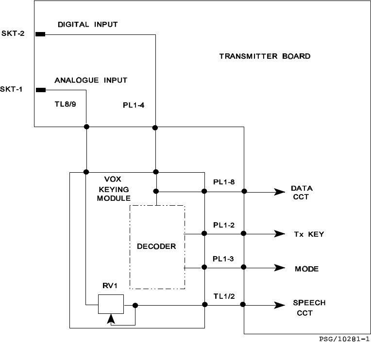
VOX KEYING MODULE
General
17. The VOX keying module decodes encoder presented serial data and controls the
transmitter. Interconnection between the Transmitter PCB and VOX Keying PCB is
as shown in Figure 2.
Figure 2: Module Interconnection Diagram
Analogue Path
18. Analogue signals are input via external connector SK1 of the transmitter PCB and
internal connectors TL8 and TL9. The level is adjusted via RV1 (VOX keying
module PCB) and output is via connectors TL1 and TL2 to the speech input of the
transmitter PCB. This presents the correct audio level to the transmitter modulation
circuits.
Data Mode
19. Data signals are input via external connector SK2 of the transmitter PCB, buffered
by TR14 and then fed, via the internal connector PL1-4, to the VOX keying module.

RPT 633
TM1184 Issue 1Page 3 - 7
Decoding
20. The VOX keying module decodes the incoming encoder serial data into the two
logic signals shown in Table 1.
Table 1: VOX Keying and Mode Signals
NOTE: Tx KEY is active low.
Tx KEY MODE TRANSMITTER
(PL1-2) (PL1-3) STATE
Low Low Data Mode
Low High Speech Mode
High Low/High Off
OPERATION
General
21. Components IC1a and IC1b are negative edge retriggerable monostables having
output pulse widths of 4.5ms (OA) for the Mode signal and 2ms (OB) for the CLK
signals to IC2. TR1 and associated components are not used in these transmitters
and are therefore by-passed via LK1 and LK2.
Power-Up
22. At power-up R4 and C5 hold IC2 CLR input low. This causes IC2 pin 3 (QC) to
route a low signal to IC3-6. Integrated circuit IC1a-6 routes a low signal to IC3-5,
which results in the Tx Key signal at PL1-2 remaining high and holding the
transmitter keyed off.
Data Path
23. To key the VOX keying module for data mode, the incoming data stream, via PL1-
4, LK1, LK2, TP2 to IC1a-5, retriggers IC1a for the duration of the data. IC1a-7
routes a low Mode signal via PL1-3 to set the transmitter into data mode whenever
data is present. Integrated circuit IC1a-6 (OA) routes a high signal to IC3-5. This
results in a low Tx Key signal via LK4 illuminating D3 and, via PL1-2, Keying
on the transmitter.
RPT 633
Page 3 - 8TM1184 Issue 1
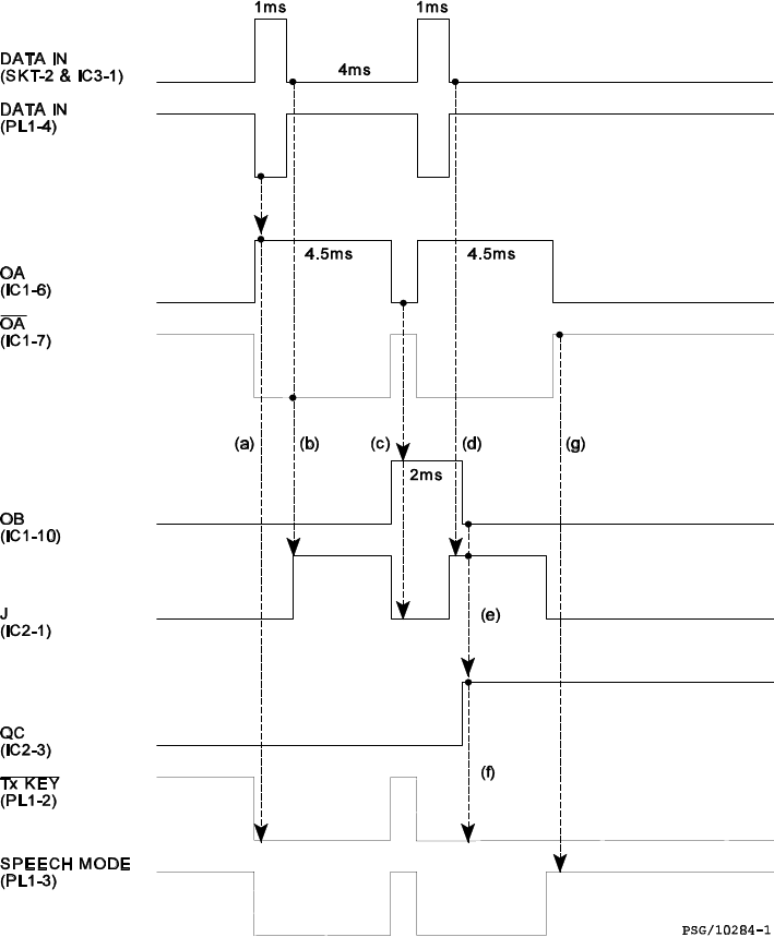
Switching to Speech
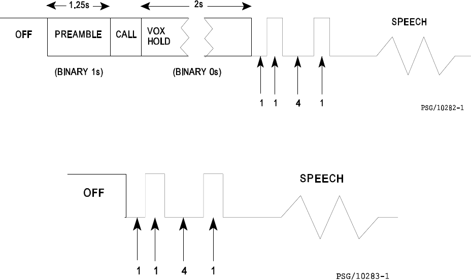
24. To switch into the speech mode, either as part of a speech paging call or for open
channel speech, the encoder generates two 1ms pulses 4ms apart as shown in
Figures 3 and 4.
Figure 3: Speech Call
Figure 4: Open Channel Speech
25. The pulses are inverted at PL1-4 and the leading edge of the first pulse results in
IC1-6 (OA) going high which switches PL1-2 low for 4.5ms (see Figure 3). The
trailing edge of the first pulse results in IC1-7 and IC3-1 presenting two lows to IC3-
12 and IC3-11 respectively, so that IC2-1 goes high. This has no immediate effect
on the circuit since the resetting of IC1a after 4.5ms removes one of the two low
states which caused J to go high.
26. The negative-going edge at IC1-6 clocks IC1b so that IC1-10 goes high for 2ms.
The trailing edge of the second pulse sets IC2-1 high again, but this time IC1b
resets after 2ms, clocking IC2-12 and resulting in IC2-3 going high. This ensures
that IC3-4 remains low during the speech mode.
27. 4.5ms after the commencement of the second pulse, IC1-7 resets high so that the
transmitter is now keyed in the speech mode.
28. Timings of IC1a and IC1b, controlled by RV2 and RV3 respectively, are absolutely
crucial to the reliable switching of the circuit into speech and must be accurately
set.
RPT 633
TM1184 Issue 1Page 3 - 9
Switching from Speech to Data
29. The speech cancel signal consists of 1.25s of binary 1s. In the speech mode IC1-7
is high with the result that IC2-1 is low. The negative-going leading edge of the first
bit of data clocks IC1a so that IC1-7 goes low, switching PL1-3 to the low DATA
mode. The negative-going transition at IC1-5, IC1a times out with the result that:
a) IC1-7 goes high putting PL1-3 into the quiescent condition.
b) IC1-6 clocks IC1b for 2ms.
c) The combined lows at PL1-4 and IC1-6 result in IC2-4 going high.
30. As IC1-10 goes low again, after 2ms, it clocks IC2 with the result that IC2-3 goes
low, IC3-4 goes high and PL1-2 returns to its quiescent high condition.
Figure 5: Switching Into Speech
RPT 633
Page 3 - 10 TM1184 Issue 1
Figure 6: Switching From Speech
RPT 633
TM1184 Issue 1Page 4 - 1
SECTION 4
INSTALLATION AND COMMISSIONING
CONTENTS:
1. INTRODUCTION
INSTALLATION
2. Positioning
3. Shelf Mounting
4. Wall Mounting
5. Antenna
6. Modulation Inputs
8. Power Supply
9. COMMISSIONING
TABLES Page
1. Encoder Mounted in a Card Frame Assembly 4 - 4
2. Encoder Mounted in a Single Slot Housing 4 - 4
3. Operating Instructions 4 - 5
FIGURES
1. Mounting Hole Diagram 4 - 2
2. Rear Panel Connections 4 - 3
3. Typical Access 340 System Configuration 4 - 3
_______________________
INTRODUCTION
1. Section 4 of this manual details the Installation and Commissioning procedures to
be carried out on a new equipment.
155
105
Dimensions in mm
PSG/10290-1
RPT 633
Page 4 - 2TM1184 Issue 1
INSTALLATION
Positioning
CAUTION
DO NOT MOUNT OVER A HEATER OR RADIATOR, OR IN DIRECT SUNLIGHT
AND ENSURE A DRY ENVIRONMENT.
2. Carefully unpack the transmitter, power supply and antenna. Site the transmitter and
power supply in a convenient working position within reach of an AC power outlet
and within 1km of the encoder.
Shelf Mounting
3. Lay the transmitter on a suitable horizontal shelf on its integral mounting feet
(sloping panel upwards). Connect the antenna as indicated in paragraphs 5 or 6
and the remainder of the electrical connections as paragraph 7.
Wall Mounting
4. Mark and drill the wall as shown, suitable for No 8 plugs and round-head screws.
Insert screws into plugs with the top of the screw head a maximum of 10mm from
the wall and the bottom of the screw head a minimum of 5mm from the wall.
Remove the rubber pads from the bottom of the base tray and hook the transmitter
onto the screws. The transmitter can be mounted either antenna up or antenna
down.
Figure 1: Mounting Hole Diagram
RED & WHITE
LEADS
BLACK LEADS
TELEPHONE
JUNCTION
BOX OR
SOCKET
POWER
SUPPLY
POWER
SUPPLY
0301-0193
OR
0360-9602
TRANSMITTER
RPT 633
TERMINAL
BLOCK
0360-8623
ANALOGUEANALOGUE
DIGITAL DIGITAL
ENCODER
RPE 340/341
DTMF/
MODEM/
SPEECH
DATA/
DLC
PSU
PSG/10287-1
RPT 633
TM1184 Issue 1Page 4 - 3
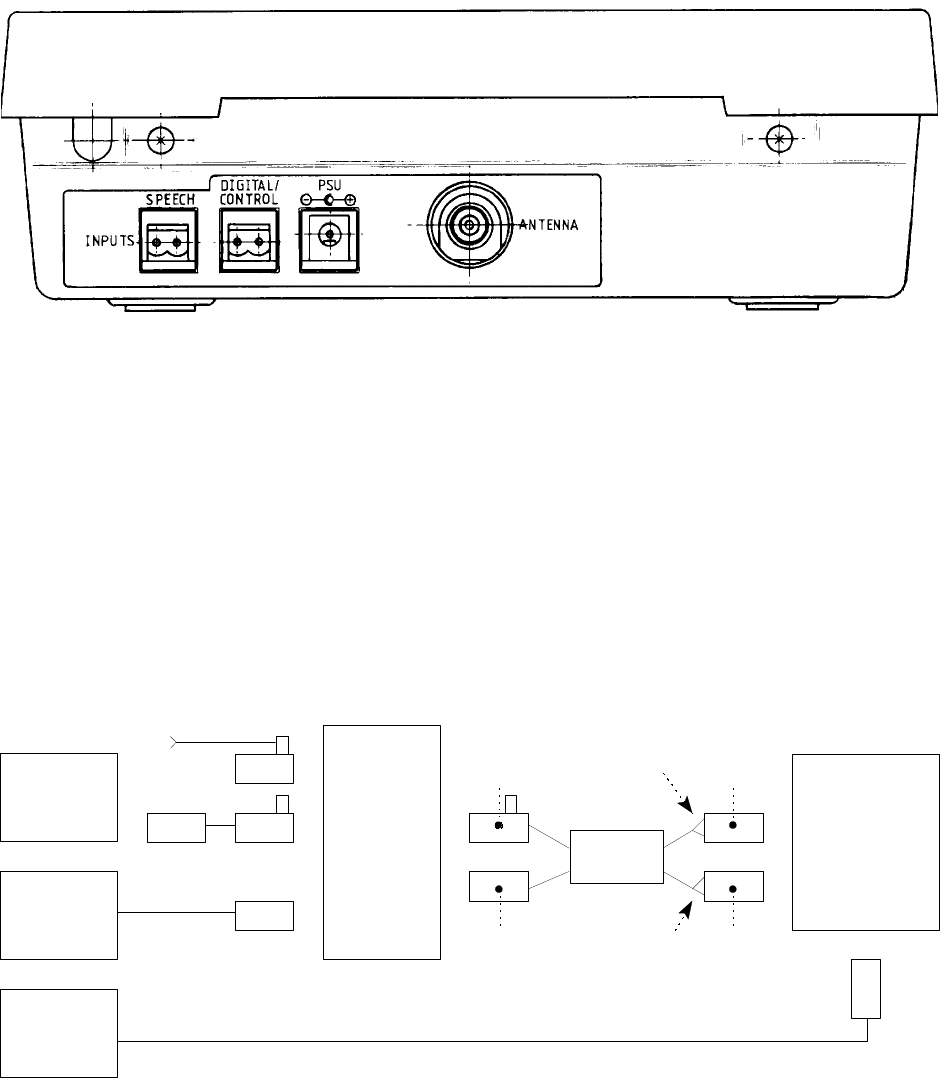
Antenna
5. Two versions of the UHF antenna are available, a straight vertical whip for wall
mounted transmitters and a right angled whip for shelf mounted transmitters.
Figure 2: Rear Panel Connections
Modulation Inputs
6. When connecting the transmitter to an RPE 340 series encoder, SK1 and SK2
should be connected as shown in Figure 3.
Figure 3: Typical Access 340 System Configuration
TEL I/F

RPT 633
Page 4 - 4TM1184 Issue 1
7. When connecting an RPT 633 transmitter to a Access 3000, it is first necessary to
use Engineering Mode Test 50 to configure the Encoder into the Non-DTMF mode.
The connections shown in Table 1 and 2, as applicable, should then be made
between the encoder and transmitter.
Table 1: Encoder Mounted in a Card Frame Assembly
SIGNAL ENCODER D TYPE CABLE COLOUR *TRANSMITTER
NAME PIN No. PIN No. TYPE CODE INPUT
Data 29c 9 }0401-0009 {Orange } SKT2 {left
0V 30a 23 } { White/Blue }{right
Speech {12a 17 }0401-0011 {Violet } SKT1 {right
{12c 4 } { Yellow }{left
* As seen from the rear of the transmitter.
Table 2: Encoder mounted in a Single Slot Housing
SIGNAL ENCODER CABLE COLOUR *TRANSMITTER
NAME PIN No. TYPE CODE INPUT
MODULAR
JACK
PIN No.
Data 29c 7}0301-0092 {Yellow } SKT2 {left
0V 30a 6 } { Blue }{right
Speech {12a 2 }0301-0091 {Orange } SKT1 {right
{12c 4} { Red }{left
* As seen from the rear of the transmitter.
8. Power Supply
Ensure that the power supply is correctly rated for your application and has the
correct mains connector. Insert the power supply outlet plug into SK3 at the rear
of the unit and plug the supply into the mains socket.

RPT 633
TM1184 Issue 1Page 4 - 5
COMMISSIONING
9. Refer to Table 3 and carry out the operating procedures as detailed for the
RPT 633 transmitter.
Table 3: Operating Instructions
ENCODER REFERENCE
Access 1000 } LCU Operator's Guide
Access 3000 } 9261-0382 or 9261-0682
RPE 340 } TM1158, Section 2, paragraphs 19-40
RPE 341 }
RPE 340A TM1154, Section 4, paragraph 4.3
RPE 350 TM1164, Section 4, paragraph 11
RPT 633
Page 4 - 6TM1184 Issue 1
INTENTIONALLY BLANK
RPT 633
TM1184 Issue 1Page 5 - 1
SECTION 5
SERVICING
CONTENTS:
1. INTRODUCTION
2. REPAIR POLICY
3. TEST EQUIPMENT
DISMANTLING AND RE-ASSEMBLY INSTRUCTIONS
4. Access to Circuit Boards
5. Removing the VOX Keying Module
6. Removing the Transmitter Board
7. Re-Assembly
TRANSMITTER BOARD ALIGNMENT PROCEDURE
8. Initial Settings
9. Initial Connections
10. Setting up Phase Lock Loop
11. Transmitter Alignment
12. Setting Data Deviation and Centre Frequency
13. Setting Analogue Modulation
14. VOX KEYING MODULE ALIGNMENT PROCEDURE
ANTENNA CUTTING
15. Introduction
16. Cutting
17. FAULT-FINDING
TABLES Page
1. Data Deviation 5-7
2. Analogue Deviation 5-8
3. Antenna Lengths 5-9
4. Test Points 5-10
RPT 633
Page 5 - 2TM1184 Issue 1
CONTENTS: (Continued)
FIGURES Page
1. Transmitter Layout: Variables, Links and Test Points 5-4
2. Antenna Cutting 5-9
_______________________
INTRODUCTION
1. Section 5 details the dismantling and reassembly instructions, alignment procedure
and the test equipment required to carry out the procedure. The transmitter contains
two printed circuit boards (PCB's). It is recommended that field service engineers
carry one complete VOX Keying Module for on-site replacement and subsequent
base repair of the faulty board.
REPAIR POLICY
2. In Section 6 is a list of spare parts for servicing the transmitter board down to
component level. Passive chip components (capacitors and resistors) are unlikely
to contribute to failure of the equipment in the field. Chip transistors and diodes
should be ordered in strips of 10 or more. A replacement antenna will need to be
cut to length before fitting, according to the information given in paragraph 17.
TEST EQUIPMENT
3. The following test equipment is required to carry out the repair procedure.
CDC Power Supply 18V, 1A.
CAbsorption Wattmeter, 5W 420-470MHz,
or
CThruline RF Power Meter 5W, 420-470MHz with Power Attenuator 5W,
20-30dB.
CFrequency Counter 500MHz, accuracy 1 part in 10 or better.
7
CAudio Signal Generator.
CModulation Meter.
COscilloscope.
RPT 633
TM1184 Issue 1Page 5 - 3
DISMANTLING AND RE-ASSEMBLY INSTRUCTIONS
CAUTION
STATIC SENSITIVE DEVICES ARE USED WITHIN THIS EQUIPMENT. CARE
MUST BE TAKEN TO ENSURE DAMAGE TO THESE DEVICES IS NOT
CAUSED BY HIGH LEVELS OF STATIC ELECTRICITY. SPARE BOARDS OR
COMPONENTS SHOULD BE STORED IN ANTI-STATIC PACKAGING WHEN NOT
INSTALLED IN THE EQUIPMENT.
Access To Circuit Boards
4. Disconnect the antenna and connectors from the rear of the case. At the rear of the
unit unscrew and remove the two retaining screws. Lift the top cover at the rear and
invert it so that it slides under the base from the front, ensuring that the ribbon
cable and the two screened cables are not strained.
Removing the VOX Keying Module
5. Disconnect the ribbon cable at the keying module. De-solder the two screened
cables at the transmitter board. Remove the four screws which secure the keying
module to the lid and remove the module.
Removing the Transmitter Board
6. Disconnect the ribbon cable at the transmitter board. De-solder the two screened
cables at the transmitter board. Remove the four nuts which secure the board to the
base and remove the board.
Re-Assembly
7. Re-assembly is the reverse of the procedure for dismantling.
RPT 633
Page 5 - 4TM1184 Issue 1
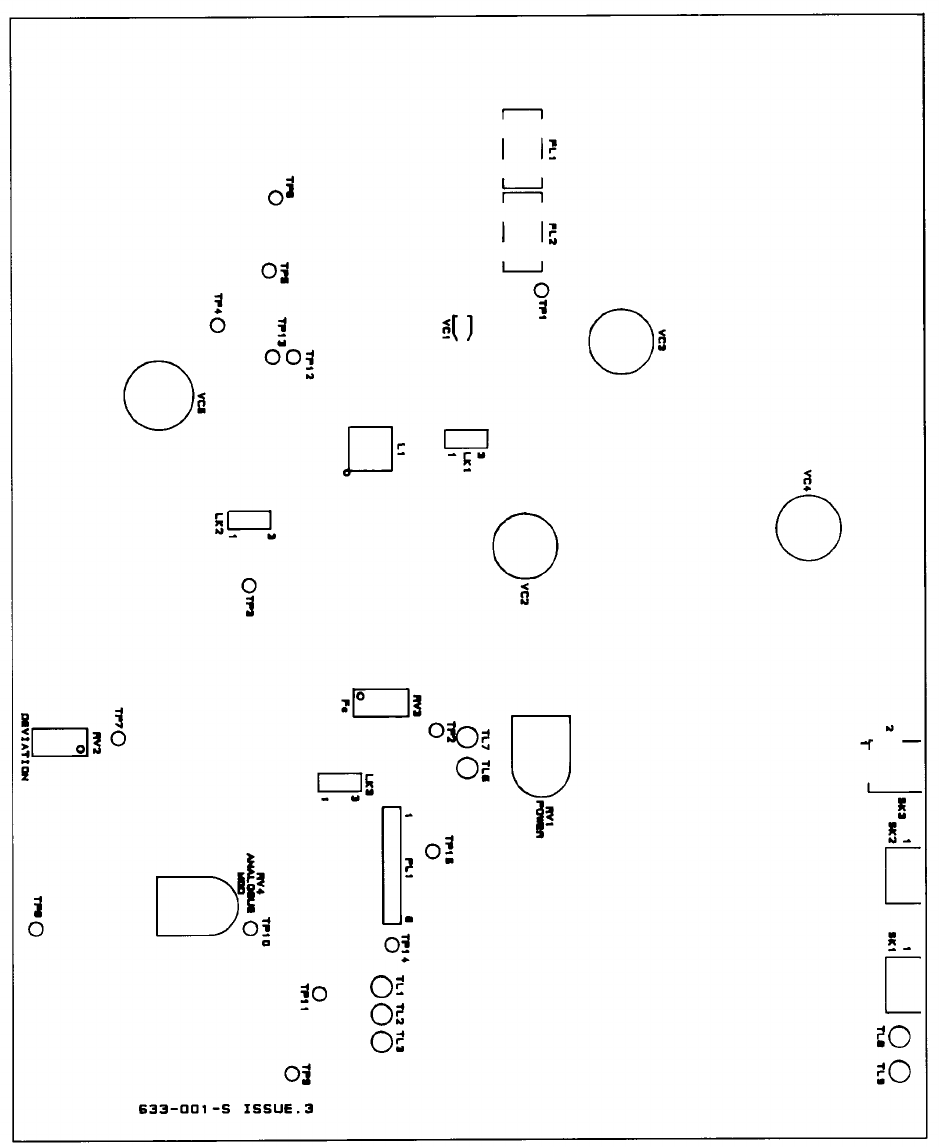
Figure 1: Transmitter Layout: Variables, Links and Test Points
RPT 633
TM1184 Issue 1Page 5 - 5
TRANSMITTER BOARD ALIGNMENT PROCEDURE
Initial Settings
8. Set the variable components and links as follows:
VC1 -Anywhere.
VC2 -Half Meshed.
VC3 -Fully Un-meshed.
VC4 -Fully Un-meshed.
VC5 -25% Meshed.
FL1 and FL2 - Adjusters standing proud by 2mm.
RV1 -Fully Anti-clockwise.
RV2 -Mid Position (15 turns from either end).
RV3 -Anywhere
RV4 -Mid Position
LK1 -Position 2-3 Normal Version.
Position 1-2 FTZ Version.
LK2 -Position 1-2 Output frequencies less than 447MHz.
Position 2-3 Output frequencies greater than or equal to 447MHz.
LK3 -Position 2-3 Normal Operation.
Position 1-2 Invert Data Sense.
Initial Connections
9. Set up the test equipment as follows:
a) Connect the absorption wattmeter or power meter to the antenna socket using
a lead no longer than 300mm.
b) Connect the modulation meter and frequency counter to the attenuated output.
c) Connect the power supply to SK3.
d) Connect the audio signal generator via a 0.47µF capacitor to SK1.
RPT 633
Page 5 - 6TM1184 Issue 1
Setting up Phase Lock Loop
10. Set up the Phase Lock Loop as follows:
a) Switch on the power supply.
b) Connect the oscilloscope to TP3.
c) Adjust the slug of L1 to give 5V ±0.2V DC at TP3.
Transmitter Alignment
11. To align the transmitter carry out the following procedure:
a) Connect the oscilloscope to TP7.
d) Adjust RV3 to give 0V ±50mV DC at TP7.
c) Key ON the transmitter by shorting TP2 to TP9.
d) On FL1 and FL2 turn the four adjusters ½ turn at a time until the power meter
indicates or the power supply current increases.
e) If no power appears slightly adjust VC2 or VC3 and repeat (d).
f) Tune the four adjusters of FL1 and FL2 for maximum power.
g) Tune VC1, VC2 and VC3 for maximum power and then RV1 to give a power
meter reading of 2.5W.
h) Re-adjust VC1, VC2 and VC3 for maximum power then RV1 for 2.5W ±0.2W.
Setting Data Deviation and Centre Frequency
12. To set the data deviation and centre frequency carry out the following procedure:
NOTE: The purpose of this adjustment is to set the deviation, i.e. for 25kHz
channel spacing, to ±4.5kHz (9kHz total) when the data polarity switch is
set from "1" to "0".
a) Set LK3 of the VOX keying module to AB to select the DATA mode.
b) Connect TP14 to TP15 (+5V) to select the binary 1 state.

RPT 633
TM1184 Issue 1Page 5 - 7
c) Measure the output frequency to the nearest 10Hz; switch the data polarity to
the binary O state by connecting TP14 to TP9 and again measure the output
frequency. Adjust RV2 and repeat this process until the difference between the
two frequencies is as given in the TOTAL DEVIATION column in Table 1 for the
appropriate transmitter channel spacing, with a tolerance of ±100Hz.
d) Using a plastic trimming tool adjust VC5 until the mean of the two frequencies
measured at (c) is within 100Hz of the specified center frequency of the
transmitter.
e) Repeat sub-paragraphs (c) and (d) as necessary.
f) Switch the mode switch to ANALOGUE by setting LK3 on the VOX keying
module to AC and adjust RV3 to give the specified centre frequency of the
transmitter to a tolerance of ±100Hz.
Table 1: Data Deviation
CHANNEL DEVIATION TOTAL
SPACING DEVIATION
kHz kHz kHz
25 ±4.5 9
20 ±3.6 7.2
12.5 ±2.25 4.5
10 ±1.8 3.6
Setting Analogue Modulation
13. To set the analogue modulation carry out the following procedure:
a) Set LK3 of the VOX keying module to AC to select the ANALOGUE mode.
d) Set the audio generator output to 1.25kHz at a level of approximately 11mV
peak-to-peak as measured on the oscilloscope. Monitor the deviation on the
modulation meter.
c) Refer to Table 2(a) and adjust the generator output level to give give a
deviation corresponding to the channel spacing.
d) Increase the signal generator output level by 20dB and adjust RV4 to give a
deviation coresponding to that given in Table 2(b). This should be the larger of
the Peak + or Peak - readings on the modulation meter.
e) Reduce the signal generator level by 20dB and re-adjust its level to give a
deviation corresponding to that given in Table 2(c).

RPT 633
Page 5 - 8TM1184 Issue 1
f) Increase the signal generator level by 20dB and re-adjust RV4 to give a
deviation corresponding to that given in Table 2(b).
g) Vary the signal generator frequency between 300Hz and 2.5kHz and check that
the deviation does not exceed that given in Table 2(d). If it does, tune to the
frequency that gives the maximum deviation and adjust RV4 to give a deviation
corresponding to that given in Table 2(e). This should also be the larger of the
Peak + or Peak - readings.
Table 2: Analogue Deviation
CHANNE DEVIATION DEVIATION DEVIATION DEVIATION DEVIATION
L(a) (b) (c) (d) (e)
SPACING kHz kHz kHz kHz kHz
kHz
25 ±3 4.75 ±3 54.9
20 ±2.4 3.8 ±2.4 43.9
12.5 ±1.5 2.4 ±1.5 2.5 2.4
10 ±1.2 1.85 ±1.2 21.9
VOX KEYING MODULE ALIGNMENT PROCEDURE
14. To set the timing circuits of the VOX Keying Module carry out the following
procedure:
a) With the RPE340 in the Engineering Mode, initiate Function 2, RPT calibration
signal. Alternatively use a P391 Test A7 to generate the same signal.
b) Monitor TP6 and adjust RV2 so that the mark/space ratio is 4.4/3.6ms.
c) Monitor TP3 and adjust RV3 so that the mark/space ratio is 2.6/5.4ms.
ANTENNA CUTTING
Introduction
15. In the event of damage to the antenna, the replacement will require cutting to length
in accordance with the following instructions.
Cutting
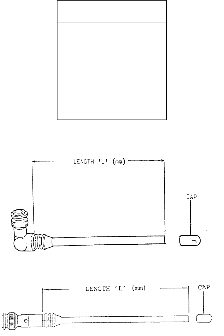
16. The antenna is a one piece UHF stub with internal connector. With reference to
Figure 1 after removal of the cap, the antenna should be cut to the length indicated
in Table 3, depending on frequency, and the cap replaced. The Part Numbers of
the uncut stubs are 5501-0001 (right angled) and 5501-0002 (straight).
RPT 633
TM1184 Issue 1Page 5 - 9
Table 3: Antenna Lengths
CUT LENGTH FREQUENCY
mm MHz
156 420
154 425
152 430
150 435
149 440
147 445
145 450
143 455
142 460
140 465
139 470
Figure 2: Antenna Cutting

RPT 633
Page 5 - 10 TM1184 Issue 1
GREAT CARE MUST BE TAKEN TO AVOID BREAKING OPEN THE
ENCAPSULATION OF TR10 ON THE TRANSMITTER BOARD WHEN REPAIR OR
COMPONENT REPLACEMENT IS BEING CARRIED OUT, AS THIS COMPONENT
CONTAINS TOXIC BERYLLIUM OXIDE.
FAULT-FINDING
WARNING
17. Table 4 shows the signals to be expected at the various test points as an aid to
fault-finding.
Table 4: Test Points
T.P. SIGNAL
1 Carrier Frequency
2 Tx Key (low-going)
3 PLL Control Voltage (nominally 5V)
4 VCO Frequency (div. by 256)
5 Crystal Frequency
6 In-Lock (high going)
7 Modulating Signal
8 -12V
9 0V
10 Audio Signal (limited)
11 Audio Signal (un-limited)
12 Over-rides Lock Fail when connected to TP13
13 +12V
14 Data
15 +5V
RPT 633
TM1184 Issue 1Page 6 - 1
SECTION 6
SPARE PARTS LIST
CONTENTS:
1. GENERAL
2. MODULES
TRANSMITTER BOARD COMPONENTS
3. Capacitors
4. Connectors
5. Crystals
6. Diodes
7. Inductors
8. Integrated Circuits
9. Links
10. Resistors
11 Transducers
12. Transformer
13. Transistor
14. Antenna
BANDED COMPONENTS
15. Filters
16. Capacitors
VOX KEYING MODULE COMPONENTS
17. Capacitors
18. Connector
19. Diodes
20. Integrated Circuits
21. Resistors
22. Transistor
RPT 633
Page 6 - 2TM1184 Issue 1
ITEM/CIRCUIT
REFERENCE DESCRIPTION PART NO.
1. GENERAL
INSERT MOULDING SCREENED 0960-9887
8-WAY INTER CONNECT FLEXFOIL 4404-0001
MOULDING COVER 0860-9846
CLAMPING PAD ADHESIVE 1861-0225
NUT M3 19663
ESCUTCHEON 2060-9878
WASHER PLAIN M3 20662
LABEL EQUIP. 31600X7
RUBBER FEET 23MM 33996
SCREW No. 6X16MM PAN HD POZI AB 8204-0616
2. MODULES
ASSY PCB VOX KEYING MODULE 0260-7083
PSU 240V UK PLUG 0301-0605
PSU 220V EURO PLUG 0301-0606
PSU 110V 0301-0607
TRANSMITTER BOARD COMPONENTS
3. Capacitors
C1,10,12,40,80 CAP CHIP 220p 10% 50V 3301-0150
C2,47,72,74,111,117 CAP AL 10F 20% 16V 3401-0089
C3,7,15,18,19,22,23,24,27,30 CAP CHIP 1n 10% 50V 3301-0100
C4 CAP CHIP 1p 0.25p 50V 3301-0001
C5,53,55 CAP CHIP 3p9 0.25p 50V 3301-0008
C8,62,63,64,108,109 CAP AL 4F7 20% 25V 3401-0093
C9,90,91,92,93 CAP AL 22F 20% 16V 3401-0090
C11 CAP CHIP 4p 0.25p 50V 3301-0151
C13,35 CAP CHIP 10p 0.25p 50V 3301-0013
C14,54 CAP CHIP 1p8 0.25p 50V 3301-0004
C16,17,36,67,68,75,79,85,87 CAP CHIP 4n7 10% 50V 3301-0108
C20,38,41,46,49,52,66,95 CAP CHIP 100n -20+80% 25V 3301-0149
C21,26,32,34,43,48,61,78,88,94,
102 CAP CHIP 220p 10% 50V 3301-0081
C25,60 CAP CHIP 5p6 0.25p 50V 3301-0010
C28,29 CAP CHIP 33p 5% 50V 3301-0025
C31,33,73,76,77 CAP CHIP 1n 10% 50V 3301-0100
C39,118,129 CAP CHIP 10n 10% 50V 3301-0112
C42 CAP CHIP 22p 5% 50V 3301-0021
C44 CAP CHIP 4p7 0.25p 50V 3301-0009
C45,70,116 CAP CHIP 1F 20% 16V 3306-0020
RPT 633
TM1184 Issue 1Page 6 - 3
ITEM/CIRCUIT
REFERENCE DESCRIPTION PART NO.
3. Capacitors (Continued)
C50,56,57 CAP CHIP 3p3 0.25p 50V 3301-0007
C51,89,113,132,133 CAP CHIP 47p 5% 50V 3301-0029
C58 CAP CHIP 6p8 0.25p 50V 3301-0011
C59 CAP CHIP Op75 0.25P 50V 3301-0251
C65 CAP AL 1000F -10+50% 40V 3402-0001
C69 CAP CHIP 2n2 10% 50V 3301-0104
C71,100 CAP POLYTR 330n 10% 63V 3304-0010
C81 CAP CER 180p N750 100V 3302-0231
C82 CAP CER 150p 2% 100V 3302-0151
C83,84 CAP CER 22p 2% 100V 3302-0141
C86 CAP CHIP 8p2 0.25p 50V 3301-0012
C96,101 CAP PLYPRP 6n8 2.5% 63V 3303-0003
C97,120,122 CAP CHIP 180p 5% 50V 3301-0043
C98,104 CAP PLYPRP 10n 2.5% 63V 3303-0004
C99,103 CAP PLYPRP 4n7 2.5% 63V 3303-0002
C105,107,114,115,124,125,126 CAP CHIP 220p 10% 50V 3301-0081
C106 CAP PLYPRP 2n2 2.5% 100V 3303-0009
C110,112,128,131 CAP CHIP 100n -20+80% 25V 3301-0149
C119 CAP AL 100F 20% 6.3V 3401-0084
C127,130 CAP CHIP 220p 10% 50V 3301-0081
VC1 CAP CHIP TRIM 10p 3506-0002
VC2,3,4 CAP VARIABLE 2-10p 3501-0002
VC5 CAP VARIABLE 4-40p 3501-0005
4. Connectors
SK1,2 PLUG 2-WAY 4501-0002
SK3 SOCKET 2.1mm PCB MOUNT 4431-0012
SK4 SKT RF COAX PANEL 4414-0001
SOCKET 2-WAY 4501-0001
5. Crystals
XL1 XTAL GENERIC SPEC 3904
XL1 XTAL GENERIC SPEC (HIGH STABILITY) 3905
OV1 CRYSTAL OVEN PLC1-27-12-75 6201-0001
6. Diodes
D1 DIODE VARICAP KV1310A-3 DUAL 3701-0027
D2 DIODE ZENER CHIP BZX84C10 3703-0017
D3,4 DIODE CHIP BAR 18 3703-0004
D5 DIODE CHIP BAV99 3703-0001
RPT 633
Page 6 - 4TM1184 Issue 1
ITEM/CIRCUIT
REFERENCE DESCRIPTION PART NO.
6. Diodes (Continued)
D6,7 DIODE ZENER CHIP BZX84C5VI 3703-0010
D8 DIODE MV2109 3701-0001
D9,10,11 DIODE CHIP BAT54 3703-0044
7. Inductors
L1 COIL MC111 SERIES 4609-0001
L2 INDUCTOR 2F2H 4102-0009
L3,4 INDUCTOR 470nH 4102-0005
L5 INDUCTOR 10TURN 4160-6235
L6 AIR COIL 4160-6236
L7 AIR COIL 4160-6237
L8,9,11,12 INDUCTOR 220nH 4102-0003
L10,19,20,21 INDUCTOR 22nH 4102-0050
L13 INDUCTOR 100nH 4102-0001
L14,15,16 ASSY COIL 605753
L17,18 INDUCTOR 1mH 4102-0025
L22 INDUCTOR 6F84107-0002
8. Integrated Circuits
IC1 IC 560CDP 3803-0003
IC2 VOLT REG 78L82AWC 95520
IC3,4 VOLT REG 7812C 6001-0002
IC5 VOLT REG 7805 6001-0001
IC6 IC 74HCTO5 3819-0014
IC7 IC 14568BCP 3802-0001
IC8 IC HEF4069 SMD HEX INVERTER 3819-0007
IC9 IC SP4660DP 3803-0001
IC10,12 IC OP. AMP. LM348D 3819-0003
IC11 IC 7661 3803-0025
IC13 IC OP AMP MC 1458ND 3818-0001
IC14 VOLTAGE REG ICL8069.REF:1.2V 6002-0026
9. Links
LK1,2,3 2-WAY JUMPER LINK (GOLD PLATED) 4408-0001
RPT 633
TM1184 Issue 1Page 6 - 5
ITEM/CIRCUIT
REFERENCE DESCRIPTION PART NO.
10. Resistors
R1 RES CHIP 15k 5% 0.125W 3101-0174
R2,12,17,63 RES CHIP 2k2 5% 0.0625W 3105-0179
R3,52,96 RES CHIP 68R 5% 0.0625W 3105-0143
R4,6,9,14,24,47,61,62,80,87 RES CHIP 6k8 5% 0.0625W 3105-0191
R5,7,8,64,73 RES CHIP 33k 5% 0.0625W 3105-0207
R10,26,59,90 RES CHIP 560R 5% 0.0625W 3105-0165
R11 RES CHIP 22R 5% 0.0625W 3105-0131
R13 RES CHIP 3k3 5% 0.125W 3101-0158
R15,45,86 RES CHIP 15k 5% 0.0625W 3105-0199
R16,67,68,69,79,100 RES CHIP 10k 5% 0.0625W 3105-0195
R18,19,37 RES CHIP 220R 5% 0.0625W 3105-0155
R20 RES CHIP 3k9 5% 0.0625W 3105-0185
R21 RES CHIP 10R 5% 0.125W 3101-0098
R22 RES CHIP 100R 5% 0.125W 3101-0122
R23,25,29,74,109,115 RES CHIP 4k7 5% 0.0625W 3105-0187
R27,34 RES CHIP 47R 5% 0.0625W 3105-0139
R28,39,40,99 RES CHIP 33R 5% 0.0625W 3105-0135
R30,33,106 RES CHIP 470R 5% 0.0625W 3105-0163
R31 RES CHIP 15R 5% 0.0625W 3105-0127
R32,91 RES CHIP 1k2 5% 0.0625W 3105-0173
R35,104 RES CHIP 10R 5% 0.0625W 3105-0123
R36 RES CHIP 18k 5% 0.0625W 3105-0201
R41,42 RES MF 100R 1% 0.6W 3103-0188
R43,53,58,117,119 RES CHIP 100R 5% 0.0625W 3105-0147
R44,84,124 RES CHIP 22k 5% 0.0625W 3105-0203
R46,107,111,114,121,123 RES CHIP 1k0 5% .0625W 3105-0171
R48 RES CHIP 7k5 5% 0.0625W 3105-0192
R49 RES CHIP 1k5 5% 0.0625W 3105-0175
R50 RES CHIP 56k 5% 0.0625W 3105-0213
R51,55,56,57,83 RES CHIP 39k 5% .0625W 3105-0209
R54 RES MF 4R7 1% 0.6W 3103-0156
R60 RES CHIP 330R 5% .0625W 3105-0159
R66,75,77,97 RES CHIP 47k 5% .0625W 3105-0211
R65,72,88 RES CHIP 82k 5% .0625W 3105-0217
R76,89 RES CHIP 68k 5% 0.0625W 3105-0215
R81,85 RES CHIP 8k2 5% .0625W 3105-0193
R82 RES CHIP 27k 5% .0625W 3105-0205
R92,101 RES CHIP 100k 5% 0.0625W 3105-0219
R93,94,98 RES CHIP 2k7 5% 0.0625W 3105-0181
R95 RES CHIP 330k 5% 0.0625W 3105-0231
RPT 633
Page 6 - 6TM1184 Issue 1
ITEM/CIRCUIT
REFERENCE DESCRIPTION PART NO.
10. Resistors (Continued)
R102 RES CHIP 820R 5% .0625W 3105-0169
R103,110,113,122 RES CHIP 10k 5% 0.0625W 3105-0195
R105 RES CHIP 1k8 5% 0.0625W 3105-0177
R108 RES CHIP 6k8 5% .0625W 3105-0191
R116 RES CHIP 3k3 5% 0.0625W 3105-0183
R118,120 RES CHIP 150R 5% .0625W 3105-0151
TH1 THERMISTOR 10k 3211-0002
RV1 POT CERMET 100R 3202-0001
RV2 POT MULTITURN 10k 3208-0010
RV3 POT MULTITURN 5k 3208-0009
RV4 POT CERMET 2k2 3202-0005
11. Transducer
LS1 TRANSDUCER 5001-0001
12. Transformer
T1 ASSY TRANSFORMER 0460-6222
13. Transistors
TR1,13,14 TRANS BCW61C 3602-0018
TR2 TRANS MMBFU 310 3602-0008
TR3,12 TRANS BCW33 3602-0010
TR4,6 TRANS BFS 17 3602-0001
TR5 TRANS BCW31 3602-0011
TR7,8 TRANSISTOR BFR96-02 3601-0001
TR9 TRANSISTOR MRF559 3601-0003
TR10 TRANSISTOR MRF630 3601-0012
TR11 TRANSISTOR BFS19 3602-0003
14. Antenna
ANTENNA RPE303 5501-0001
FLEXIBLE STRAIGHT ANTENNA 5501-0002
RPT 633
TM1184 Issue 1Page 6 - 7
ITEM/CIRCUIT
REFERENCE DESCRIPTION PART NO.
BANDED COMPONENTS
15. Filters
FL1,2 FILTER HELICAL 252-MX-1547A BAND 14605-0005
FL1,2 FILTER HELICAL 252-MX-1549A BAND 24605-0006
FL1,2 FILTER HELICAL 252-MX-1551A BAND 34605-0007
16. Capacitors
C6 CAP CER 10p 0.25p 63V BAND 13302-0099
C6 CAP CER 10p 0.25p 63V BAND 23302-0099
C6 CAP CER 8p2 0.25p 63V BAND 33302-0098
VOX KEYING MODULE COMPONENTS
17. Capacitors
C1 CAP AL 22FF 20% 16V 3401-0008
C2,3,5,6,7 CAP POLYTR 100n 10% 63V 3304-0002
C4 CAP POLYTR 220n 10% 63V 3304-0009
C8 CAP AL 10F 20% 35V 3401-0100
18. Connector
PL1 8-WAY PLUG RT ANGLED 4303-0044
19. Diodes
D1,2 DIODE 1N4148 17535
D3 INDICATOR LED HLMP1700 3704-0011
20. Integrated Circuits
IC1 IC 4538 3802-0043
IC2 IC 74HC107 3801-0049
IC3 IC 74HCO2 95993
RPT 633
Page 6 - 8TM1184 Issue 1
ITEM/CIRCUIT
REFERENCE DESCRIPTION PART NO.
21. Resistors
R1 RES MF 39k 1% 0.6W 3103-0250
R2 RES MF 10k 1% 0.6W 3103-0236
R3 RES MF 680R 1% 0.6W 3103-0208
R4 RES MF 100k 1% 0.6W 3103-0260
R5 RES MF 1k5 1% 0.6W 3103-0216
R6 RES MF 47k 1% 0.6W 3103-0252
RV1 POT CERMET 2k2 3202-0005
RV2,3 POT CERMET 220k 3202-0011
22. Transistor
TR1 TRANSISTOR BC183L 95785
TM 1184 Issue 1 AL1 (May 1997) Page A1 - 1
APPENDIX 1
UHF SERIAL ENCODER MODEL RPE 673
CONTENTS
1. INTRODUCTION
2. ROLE
3. PHYSICAL CONSTRUCTION
SPECIFICATION
4. Encoder
5. Connectors
7. OPERATING INSTRUCTIONS
8. TECHNICAL DESCRIPTION
PRE-INSTALLATION CHECKS
13. Unpacking
14. Tools required
15. Test Equipment required
INSTALLATION PROCEDURE
16. Wall Mounting
17. Software Configuration
24. Parameter Definitions
26. Connecting the External Device
30. Audio Connection
31. Direct Line Contacts (DLCs)
35. Antenna
RPE 673
TM 1184 Issue 1 AL1 (May 1997)Page A1 - 2
CONTENTS (Continued)
SERVICING
37. Repair Policy
39. Removal / Re-fitting of Circuit Boards
44. Transmitter Alignment - Initial settings
46. Setting up the Phase Lock Loop
47. Transmitter Alignment
48. Setting Data Deviation and Centre Frequency
49. Setting Analogue Deviation
50. FAULT FINDING
51. ANTENNA CUTTING
52. SPARE PARTS LIST
TABLES Page
1. Encoder SK1/SK2 Pin Outs A1 - 12
2. P910 Connections A1 - 12
3. P911 Connections A1 - 13
4. DLC Connections A1 - 14
5. Data Deviation A1 - 21
6. Analogue Deviation A1 - 22
FIGURES
1. Encoder Connections A1 - 5
2. Wall Mounting Template A1 - 7
3. Set-up Menu A1 - 8
4. P910/P911 Connector Pin Layout A1 - 13
5. External Connections A1 - 15
6. Serial Encoder - Service Layout A1 - 16
7. Transmitter PCB Layout A1 - 18
8. Test Menu Options A1 - 20
9. Serial Encoder Interconnection Diagram A1 - 24
TM 1184 Issue 1 AL1 (May 1997) Page A1 - 3
INTRODUCTION
1. This Appendix outlines the installation and operation of the Radio Paging
Serial Encoder (Transmitter/Encoder) model RPE 673. The Serial Encoder utilises the
existing RPT 633 Transmitter PCB and, whenever necessary, reference is made
to the appropriate section in the main body of this manual.
ROLE
2. The Multitone RPE 673 is a single channel radio paging Serial Encoder operating in the
UHF frequency band. The Serial Encoder provides paging facilities for Mk6 or Mk7 code
format alphanumeric and speech radio paging systems. The Serial Encoder can be used
to call up to 10,000 radio paging receivers.
PHYSICAL CONSTRUCTION
3. The RPE 673 consists of an Encoder PCB combined with a 2.5W Transmitter
PCB (as used in RPT 633) together in one moulded plastic housing.
SPECIFICATION
NOTE:For Transmitter characteristics and crystal frequency calculation refer to
Section 1.
Encoder
4. The performance characteristics of the Encoder are as follows:
a) Protocol: ESPA 4.4.4. or MEP (Determined by firmware)
b) Code Format: Multitone Mk6 or Mk7 (Programmable)
c) Paging Addressees: 10,000
d) Beep Codes: Eight
e) Message Transmission: Up to 60 alphanumeric characters
f) Speech Transmission: Duration is unlimited and under the control of the
External Device (speech is applicable only when
ESPA 4.4.4. protocol is used)
RPE 673
TM 1184 Issue 1 AL1 (May 1997)Page A1 - 4
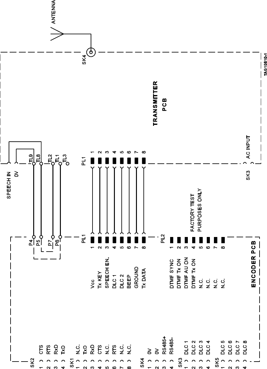
Connectors
5. The RPE 673 Serial Encoder is fitted with the following external connectors:
a) SK1: Audio Input Two pin moulded socket (600 Ohm)
b) SK2: Not Used
c) SK3: Power Supply Unit Four-way FCC68 socket
d) SK4: Antenna TNC (50 Ohm)
6. In addition, the following internal connectors are fitted to the Encoder PCB:
a) SK1: Serial Data input Eight-way FCC68 socket
b) SK2: Serial Data input Four-way IDC
c) SK3: Remote DLCs 1-4 Four-way IDC
d) SK5: Remote DLCs 5-8 Four-way IDC
e) SK4: Ground for RS232 / DLCs Four-way IDC
RS485 Data I/P (Not used)
NOTE: Physical Characteristics, Operational Environment and Power Supply
Options are identical to the RPT 633.
OPERATING INSTRUCTIONS
7. The Radio Paging Serial Encoder is fully automatic in use and operation is limited to
switching on the mains supply.
ENCODER
TRANSMITTER
PSU
AUDIO (SK1)
RS232 DATA
MODE
Tx
Rx
RTS
CTS
Tx KEY
DATA
BEEP
GND (SK4)
SK3
(SK1 or SK2)
POWER (SK3)
PL1
PL1
ANTENNA
SK4
TL9
TL8
TL2 TL1
P4 P5 P7 P6
TAG10817-1
6
8
2
3
SK5
RV1 - AUDIO ADJUST
DLCs 1 - 8
3
2
8
6
POWER
1
TM 1184 Issue 1 AL1 (May 1997) Page A1 - 5
Figure 1: Encoder Connections
TECHNICAL DESCRIPTION
NOTE: For a circuit description of the Transmitter, refer to Section 3.
8. The RPE 673 Serial Encoder provides a communications link between any device with
a standard RS232 data output and up to 10,000 paging receivers. Valid data is
processed by a purpose built digital Encoder and fed to a 2.5W UHF Transmitter (based
upon the RPT 633) for onward transmission.
9. The Encoder is driven by the serial RS232 data input (SK1 or SK2) and the eight DLC
inputs (SK3 and SK5) using ESPA 4.4.4 or MEP protocol (as determined by firmware).
Receipt of serial data or closure of any DLC causes the Encoder to enter the call
generation routine. A paging transmission is assembled in either Mk6 or Mk7 paging code
format. The format is selected during installation (refer to paragraph 24).
10. The eight DLC inputs may be used for remotely sited contacts which must close to initiate
paging calls. The DLC paging messages can be configured during installation (refer to
paragraph 24).
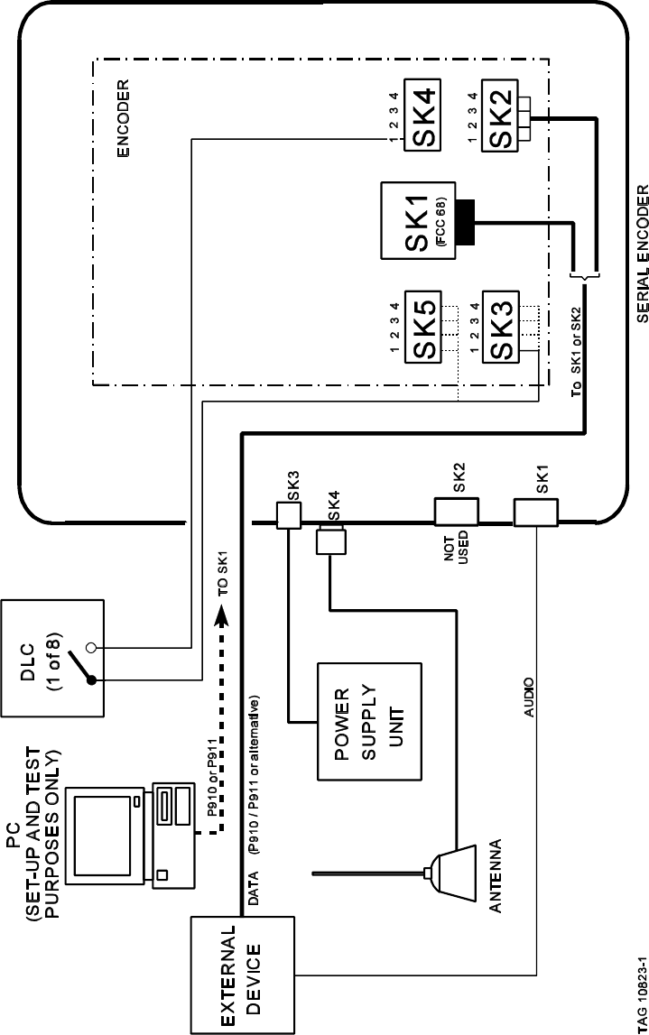
11. Figure 1 illustrates Encoder input / output connections. Power (+5V) is supplied to the
Encoder PCB from the Transmitter PCB on PL1-1 and ground is PL1-7.
12. The Encoder PCB also contains circuitry for the signal conditioning of the audio/speech
input to the Serial Encoder. PL2 on the Encoder PCB is for factory test purposes only.
RPE 673
TM 1184 Issue 1 AL1 (May 1997)Page A1 - 6
PRE-INSTALLATION CHECKS
CAUTION
STATIC SENSITIVE DEVICES ARE USED WITHIN THIS EQUIPMENT.
OBSERVE STATIC SAFETY PRECAUTIONS.
Unpacking
13. Unpack the container and examine the contents against the list given below:
a) RPE 673 Serial Encoder Unit Qty 1
b) Power Supply Unit, 3-pin plug (UK) or 2-pin (Europe) Qty 1
c) Antenna Assembly * Qty 1
d) Socket, 2-way (4501-0001) Qty 2
*Supplied only when requested on Sales Specification Form
Tools Required
14. The following tools will be required:
a) Screwdrivers - Flat and Cross-Point
b) IDC Insertion Tool
Test Equipment Required
15. The following test equipment will be required:
a) PC with RS232C serial port
b) P910 Cable Assembly, 9-Way, D-Type or
P911 Cable Assembly, 25-Way, D-Type
c) 4404-0003 Interconnect Flexible
155 mm
TAG 10821-1
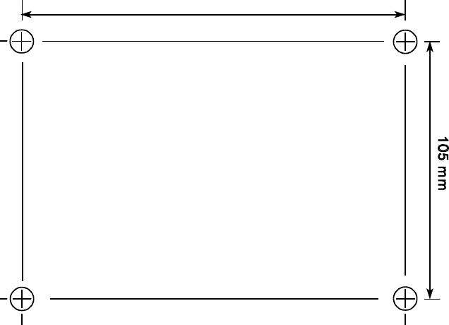
TM 1184 Issue 1 AL1 (May 1997) Page A1 - 7
Figure 2: Wall Mounting Template
INSTALLATION PROCEDURE
Wall Mounting
CAUTION
ENSURE THE UNIT IS MOUNTED IN A DRY ENVIRONMENT. DO NOT MOUNT
THE UNIT OVER A HEAT SOURCE OR IN DIRECT SUNLIGHT.
16. The unit may be mounted on a suitable horizontal shelf or wall-mounted using the
following procedure:
a) Referring to Figure 2 (or using the template supplied with the Serial Encoder), drill
holes to accept 8mm plugs and screws.
b) Fit the plugs into the holes and insert the screws into the plugs leaving 5mm
clearance between the screw heads and the wall.
c) Remove the four rubber feet from the base and slot the Serial Encoder onto the screw
heads.
NOTE:It may not be possible to carry out the Software Configuration using a
PC whilst the External Device is connected. It is recommended that
the Software Configuration is carried out before connecting the External
Device.

F - Set Code (F)ormat
T-Set (T)ime-of-Day Option
P - Change Serial (P)ort Settings
1-8 - Edit DLC 1 - 8
Setup
=====
Serial Port: 1200 Baud, 7 Data Bits, 2 Stop, Even Parity
Serial Protocol = MEP Options: Timeout = 1
Code Format: Mk 7 System Address: 0 Time-of-Day: Off Time-of-Day User No: 1234
DLC Rx No BC Message
-------------------------------------------------------
1 1111 2 ‘Message 1'
2 1230 1 ‘Message 2'
3 333G 1 ‘Message 3'
8 8910 1 ‘Message 8'
.
.
Choose:-
S - Set (S)ystem Address
U - Set Time-of-Day (U)ser
O - Change Serial Protocol (O)ptions
Q - (Q)uit
4 45GG 1 ‘Message 4'
.
.
FIRMWARE M670101
RPE 673
TM 1184 Issue 1 AL1 (May 1997)Page A1 - 8
Figure 3: Set-up Menu
Software Configuration
17. To gain access to Encoder socket SK1, remove the two cross-point screws from the
rear of the unit. Lift the cover slightly (it will only clear the base by 4 to 5 inches). Carefully
disconnect the 8-way flexi-cable from PL1 of both Transmitter and Encoder. Pivoting on
its front edge, invert the cover and slide it under the base. Fit test cable 4404-0003 to PL1
of Transmitter and Encoder.
18. Connect the serial port of your PC to SK1 (FCC 68) of the Encoder PCB using the
P910 or P911 cable. If using Windows 95, run Hyper-Terminal; if using Windows 3.1,
run Terminal.Exe. Configure your serial port as follows: 9600 Baud, 8 Data bits,
2 Stop bits, no Parity bit, Flow Control = Hardware.
19. Connect the external power supply to SK3 of the Serial Encoder. Power up the Serial
Encoder, wait 3 seconds and, within a further 10 seconds, press <Enter>; the
(S)et-up / Test Menu should appear on the VDU. Select (S)et-up; the Setup menu
should appear on the VDU (see Figure 3).
20. Having accessed the Set-up Menu the following parameters may be set:
F-Code Format S-System Address
T-Time-of-Day Option U-Time-of-Day User
P-Serial Port Settings O-Serial Protocol Options
1 - 8 -Edit DLCs Q-Quit
TM 1184 Issue 1 AL1 (May 1997) Page A1 - 9
21. Definitions for each parameter are given in paragraph 24.
22. Once a setting has been selected, the following message will be displayed:
‘....Writing to Eeprom - please wait.....Done’
and the Set-up screen will again be displayed.
23. For Serial Port Settings however, parameters are not written to the Eeprom until
‘W’ (Write to Eeprom) is selected from the Serial Port Set-up Menu.
Parameter Definitions
24. The Parameter Definitions are as follows:
DLC Each DLC has a configurable Receiver Number (Rx No), Beep Code (BC) and
Configuration Message.
a) Rx No Four digit code in the range 0000 - 9999. The Rx No will be
automatically prefixed with the System Address to form the RIC.
Group calls may be initiated in order to call a group of paging
receivers within a specified range of addresses by inserting the
wildcard character ‘G’ into the Rx No.
If one wildcard character is included as the least significant digit
then a group of 10 receivers will be called, eg: ’333G will
call receivers ’3330 to ’3339 (where ’ = SystemAddress).
If two wildcard characters are included as the two least significant
digits then a group of 100 receivers will be called, eg: ’45GG
will call receivers ’4500 to ’4599 (where ’ = System Address).
b) Beep Single digit in the range 1 - 8
Code
c) Message Mk6: Maximum length of 10 characters in the range 0 - 9,
(hyphen) and <Space>.
Mk7: Maximum length of 60 characters in the standard ASCII
character set ie,<Space> (Hex 20) through to ‘~’ (Hex7E).
Serial Port These parameters are for the V24/RS232 port and are set to match the
Settings External Device to which the Serial Encoder is connected. The selections are self
explanatory however, once the settings have been made, they must be
written to the Eeprom by entering ‘W’ ([W]rite changes to Eeprom).
NOTE: During set-up and test, the Serial Encoder communicates using a fixed
set of parameters (9600 Baud, 8 Data Bits, 2 Stop Bits, No Parity Bit).
The above Serial Port Settings only take effect during normal operation.
RPE 673
TM 1184 Issue 1 AL1 (May 1997)Page A1 - 10
Serial Protocol a) MEP: The only serial option for MEP protocol is the Timeout setting:
Options Setting Timeout Setting Timeout
0100 ms 4 4 seconds
1 1 second 5 5 seconds
2 2 seconds 6 6 seconds
3 3 seconds 7 7 seconds
NOTE: The Timeout settings are designed to allow flexibility in
the response times from different external devices.
b) ESPA: There are two options: <Turn-Round / Response Time’ and <Suppress
Response Option’.
i) Turn-Round / Response Time:
Setting Turn-Round Time Response Time
0approx 10ms 150ms
130 - 40 ms 300ms
2100ms 3s
31s 10s
NOTE: Turn Round time is a delay introduced before
transmission allowing intervening hardware, such as
convertors or modems, to change configuration or
direction.
Missed Response time is the period after transmission
that the RPE 673 waits for an acknowledgement.
ii) Suppress Response - Valid input is <0’ (disabled) or <1’
(enabled). When enabled, the automatic responses back to
the External Device from the RPE 673 will be suppressed (not
sent).
NOTE: Suppression is beneficial if the operation of the
RPE 673 is slow.
Code Format Determines the digital data format (Mk6 or Mk7) to be sent by the Serial Encoder.
Valid input is ‘6’ or ‘7’.
System Address A single numeric digit which must match the most significant digit of the Receiver
Identification Code (RIC) for the corresponding paging receiver. Valid input is 0 - 9
for Mk6 and 0 - 3 for Mk7.
Time-of-Day If set to ‘1’ (on) then Time-of-Day paging calls will be sent at one-minute intervals
Option and, Mk7 paging calls will contain an updated time-stamp.
If set to ‘0’ (off) then Time-of-Day calls will not be sent and, Mk7 calls will contain
a fixed time-stamp.
TM 1184 Issue 1 AL1 (May 1997) Page A1 - 11
Time-of-Day This is a dummy User / Receiver which is used to allow the Time and/or Date
User Number to be set. If a call is sent to this receiver then the message content is used to set
the system Time and/or Date as follows:
a) To set the Time, the Time-of-Day User is called with a 4-digit message in the
form: ‘HHMM’ where:
HH represents the Hours digits (00 - 23)
MM represents the Minutes digits (00 - 59)
b) To set the Date (Mk7 only), the Time-of-Day User is called with a 6-digit
message in the form: ‘YYMMDD’ where:
YY represents the last two digits of the Year (00 - 99)
MM represents the Month of the Year (01 - 12)
DD represents the Day of the Month (01 - 31)
c) As an alternative, a 10-digit numeric message in the form <<YYMMDDHHMM’
will set both Time and Date together.
NOTE: Mk6 paging receivers must be programmed with System Size
set to ‘10,000’ and System Type set to ‘Other’.
25. Once set-up is complete, turn off the power supply and disconnect the PC.

RPE 673
TM 1184 Issue 1 AL1 (May 1997)Page A1 - 12
Connecting the External Device
26. Connection of the External Device to the RS232 port on the Encoder can be madein on e
of two ways:
a) Connecting the P910 or P911 to Encoder SK1.
b) Connecting an alternative cable to the Krone connections on Encoder SK2.
27. Note that Encoder SK1 and SK2 are connected in parallel; only one socket can be
utilised.
28. Pin out details of Encoder sockets SK1 and SK2 are shown in Table 1.
Table 1: Encoder SK1 / SK2 Pin Outs
SK1 (FCC 68) SK2
Pin 1 Ground Pin 1 CTS
Pin 2 TxD Pin 2 RTS
Pin 3 RxD Pin 3 RxD
Pin 4 CTS Pin 4 TxD
Pin 6 RTS
NOTE: If connecting the External Device to SK2, a return connection (signal
ground) should be made to 0V on SK4 (pin 1 or pin 2) of the Encoder PCB.
29. Connection details for cable assemblies P910 and P911 are shown in Tables 2 and 3.
Pin layout is illustrated in Figure 4.
Table 2: P910 Connections
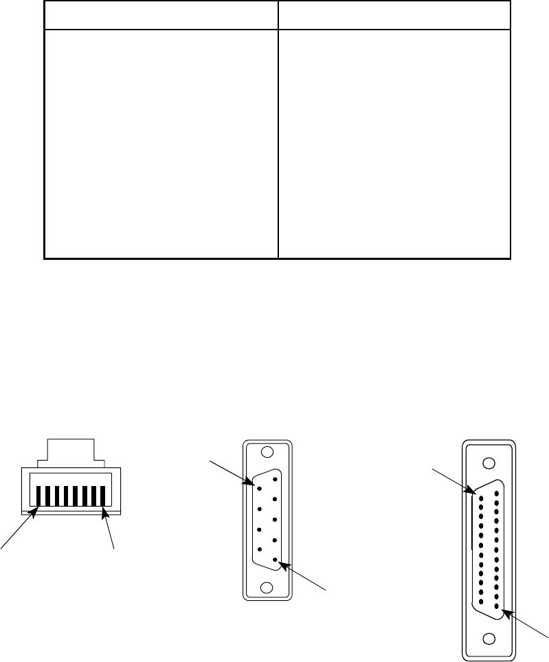
8 Way Modular Jack Plug 9 Way D-Type Connector
Pin 1 Pin 5 Signal Ground
Pin 2 Pin 2 Transmit Data
Pin 3 Pin 3 Receive Data
Pin 4 Pin 7 CTS
Pin 5 Pin 6 N.C.
Pin 6 Pin 8 RTS
Pin 7 Pin 4 N.C.
Pin 8 Pin 1 N.C.
N.C. = Not Connected
8 WAY MODULAR
JACK PLUG (P910/911)
PIN 1 PIN 8
TAG 10829-1
PIN 25
PIN 1
25 WAY D-TYPE
CONNECTOR (P911)
PIN 1
9 WAY D-TYPE
CONNECTOR (P910)
PIN 9
TM 1184 Issue 1 AL1 (May 1997) Page A1 - 13
Figure 4: P910/P911 Connector Pin Layouts
Table 3 : P911 Connections
8 Way Modular Jack Plug 25 Way D-Type Connector
Pin 1 Pin 7 Signal Ground
Pin 2 Pin 3 Transmit Data
Pin 3 Pin 2 Receive Data
Pin 4 Pin 4 CTS
Pin 5 Pin 6 N.C.
Pin 6 Pin 5 RTS
Pin 7 Pin 20 N.C.
Pin 8 Pin 8 N.C.
N.C. =Not Connected

RPE 673
TM 1184 Issue 1 AL1 (May 1997)Page A1 - 14
Audio Connection
30. If required, the audio output from the External Device should be connected to Serial
Encoder SK1 using the 2-Way Socket, Part No. 4501-0001 (provided) and suitable cable
(RV1 on the Encoder PCB may be adjusted to compensate for the output level provided
by the audio source at the customer’s premises).
Direct Line Contacts (DLCs)
31. DLCs can be a door bell push, a security alarm, a sensor on a piece of machinery etc.
Contacts must close to initiate a paging call and should be connected to the Serial
Encoder by a twisted-pair wire.
32. The loop resistance of each DLC connection must not exceed 150 S.
33. DLC connections are listed in Table 4. Return connections are made to 0V on SK4
(pin1 or pin 2) of the Encoder PCB.
Table 4: DLC Connections
SK3SK5
Pin 1 DLC 1 Pin 1 DLC 5
Pin 2 DLC 2 Pin 2 DLC 6
Pin 3 DLC 3 Pin 3 DLC 7
Pin 4 DLC 4 Pin 4 DLC 8
34. Remove the Interconnect Cable 4404-0003 and re-fit the flexi-cable to PL1 of Transmitter
and Encoder. Replace and secure the cover.
Antenna
35. Following the manufacturer’s instructions, connect the antenna to SK4.
36. If using the Whip Antenna, stand the antenna on a flat surface and lay the connecting
lead as straight as possible to the Serial Encoder. The best transmission will be
achieved with the antenna as high as possible and preferably stood on a metal surface
such as a filing cabinet. This will achieve a good ground-plane.
TM 1184 Issue 1 AL1 (May 1997) Page A1 - 15
Figure 5: External Connections
TAG10830-1
RPE 673
TM 1184 Issue 1 AL1 (May 1997)Page A1 - 16
Figure 6: Serial Encoder - Service Layout
TM 1184 Issue 1 AL1 (May 1997) Page A1 - 17
SERVICING
Repair Policy
37. The following service policy applies to the RPE 673:
a) The Encoder PCB and the Encoder firmware device (IC2) are disposable modules;
both are available as service spares.
b) The Transmitter PCB is repairable to component level (for part numbers, refer to
Section 6).
38. Transmitter alignment procedures (paras 45 - 49) rely on the use of a PC for
Transmitter keying. For alignment procedures without the use of a PC, refer
to Section 5.
Removal / Re-fitting of Circuit Boards
39. Disconnect the antenna and connectors from the rear of the case. At the rear of
the unit unscrew and remove the two retaining screws. Lift the cover slightly (it will only
clear the base by 4 to 5 inches). Carefully disconnect the 8-way flexi-cable from PL1
of the Transmitter. Pivoting on its front edge, invert the cover and slide it under the
base.
40. To remove the Encoder board, de-solder the two screened cables from P4, P5, P6
and P7 of the Encoder PCB (see Figure 6). Remove the four screws to release the
Encoder PCB.
41. When replacing a suspect Encoder PCB with a service replacement PCB,
proceed as follows:
a) Remove the suspect Encoder PCB.
b) Remove the replacement Encoder PCB from its packaging.
c) Carefully transfer the firmware device (IC2) from the suspect Encoder PCB to
the replacement Encoder PCB.
d) Fit the service replacement Encoder PCB.
e) Carry out the Set-up procedure detailed in paras 18 - 25.
42. To Remove the Transmitter board, de-solder the two screened cables from TL1, TL2, TL8
and TL9 of the Transmitter board (see Figure 6). Remove the four securing nuts to
release the Transmitter PCB.
43. Re-assembly is the reverse of dismantling. Replace the 8-Way flexi-cable (removed in
paragraph 39) before re-fitting the cover.

TL9
RV1
TL3
TL2
TL1
TP9
TP11
TP10
RV4
TP8
RV2
TP7
LK3
RV3
TL6
TP2
TL7
VC4 VC2
TP3
LK2
LK1 L1
VC3
VC5
VC1 TP13
TP12
TP14
TP5
TP6
TP15
TP14
TP1
FL2
FL1
PL1
TL8
SK1
SK2
SK3
RPE 673
TM 1184 Issue 1 AL1 (May 1997)Page A1 - 18
Figure 7: Transmitter PCB Layout
PSG10532-1
TM 1184 Issue 1 AL1 (May 1997) Page A1 - 19
Transmitter Alignment - Initial Settings
44. Refer to Figure 7. Set the variable components and links as follows:
VC1 -Anywhere.
VC2 -Half Meshed.
VC3 -Fully Un-meshed.
VC4 -Fully Un-meshed.
VC5 -25% Meshed.
FL1 and FL2 - Adjusters standing proud by 2mm.
RV1 -Fully Anti-clockwise.
RV2 -Mid Position (15 turns from either end).
RV3 -Anywhere
RV4 -Mid Position
LK1 -Position 2-3 (Normal Version).
Position 1-2 (FTZ Version).
LK2 -Position 1-2 (Bands 1 and 2).
Position 2-3 (Band 3).
LK3 -Position 2-3 (Normal Operation).
Position 1-2 (Invert Data Sense).
45. Set up the test equipment as follows:
a) Disconnect the external audio input from SK1 on the Transmitter PCB.
b) Connect the absorption wattmeter or power meter to the antenna socket using a
lead no longer than 300mm.
c) Connect the modulation meter and frequency counter to the attenuated
output.
d) Connect the power supply to SK3.
e) Connect the audio signal generator to Serial Encoder SK1.
f) Connect the serial port of your PC to SK1 (FCC 68) of the Encoder PCB using
the P910 or P911 cable. If using Windows 95, run Hyper-Terminal; if using
Windows 3.1, run Terminal.Exe. Configure your serial port as follows: 9600 Baud,
8 Data bits, 2 Stop bits, no Parity bit, Flow Control = Hardware.
g) Connect the external power supply to SK3 of the Serial Encoder.
Set-up / Test Menu
===============
T - (T)est Menu
S - (S)et-up Menu
Q - (Q)uit T - (T)ransmitter Tests
F - (F)ull Test
Q - (Q)uit Transmitter Test Menu
M - Key up Transmitter - (M)arking
S - Key up Transmitter - (S)pacing
P - Key up Transmitter - (P)reamble
A - Key up Transmitter - (A)nalogue
Q - (Q)uit
==================
TAG 10827-1
RPE 673
TM 1184 Issue 1 AL1 (May 1997)Page A1 - 20
Figure 8: Test Menu Options
h) Power up the Serial Encoder, wait 3 seconds and, within a further 10 seconds,
press <Enter> on the Terminal keyboard; the Set-up / Test Menu should
appear on the VDU (see Figure 8).
j) Select (T)est Menu.
NOTE: The Transmitter Tests are used to key the Transmitter during
alignment, Full Test is for factory use only.
Setting up the Phase Lock Loop
46. Set up the Phase Lock Loop as follows:
a) Connect the oscilloscope to TP3.
b) Adjust the slug of L1 to give 5V ±0.2V DC at TP3.
Transmitter Alignment
47. To align the Transmitter carry out the following procedure:
a) Connect the oscilloscope to TP7.
b) Adjust RV3 to give 0V ±50mV DC at TP7.
c) Key up the Transmitter by selecting (A)nalogue.

TM 1184 Issue 1 AL1 (May 1997) Page A1 - 21
d) On FL1 and FL2 turn the four adjusters ½ turn at a time until the power meter
indicates or the power supply current increases.
e) If no power appears slightly adjust VC2 or VC3 and repeat (d).
f) Tune the four adjusters of FL1 and FL2 for maximum power.
g) Tune VC1, VC2 and VC3 for maximum power and then RV1 to give a power meter
reading of 2.5W.
h) Re-adjust VC1, VC2 and VC3 for maximum power then RV1 for 2.5W ±0.2W.
Setting Data Deviation and Centre Frequency
48. To set the Data Deviation and Centre Frequency carry out the following procedure:
a) Select (M)arking (continuous ‘1's) from the Transmitter Test Menu. Measure the
output frequency to the nearest 10Hz.
b) Select (S)pacing (continuous ‘0's) from the Transmitter Test Menu and again
measure the output frequency to the nearest 10Hz.
c) Adjust RV2 as necessary until the measurement at (b) differs from the
measurement at (a) by the amount given in the TOTAL DEVIATION column of
Table 5 (within the specified tolerance).
d) Using a plastic trimming tool adjust VC5 until the mean of the two frequencies
measured at (a) and (b) is within 100Hz of the specified centre frequency of the
Transmitter.
Table 5: Data Deviation
CHANNEL DEVIATION TOTAL TOLERANCE
SPACING kHz DEVIATION
kHz kHz
25 ± 4.5 9± 200Hz
20 ± 3.6 7.2 ± 200Hz
12.5 ± 2.25 4.5 ± 100Hz
10 ± 1.8 3.6 ± 100Hz
e) Repeat sub-paragraphs (a) to (d) as necessary.
f) Select (A)nalogue from the Transmitter Test Menu. Adjust RV3 to give the specified
centre frequency of the Transmitter (to a tolerance of ±100Hz).

RPE 673
TM 1184 Issue 1 AL1 (May 1997)Page A1 - 22
Setting Analogue Deviation
49. To set the Analogue Deviation carry out the following procedure:
a) Select (A)nalogue from the Transmitter Test Menu.
b) Set the audio generator output to 1.25kHz at a level of -13dBm (approximately
11.5mV peak-to-peak as measured on the oscilloscope). Monitor the deviation on
the modulation meter. Adjust RV1 on the Encoder PCB fully clockwise.
c) Refer to Table 6(a) and adjust the generator output level to give a deviation
corresponding to the channel spacing.
d) Increase the signal generator output level by 20dB and adjust RV4 to give a deviation
corresponding to that given in Table 6(b) (this should be the larger of the Peak ‘+’ or
Peak ‘-’ readings on the modulation meter).
Table 6: Analogue Deviation
CHANNEL DEVIATION DEVIATION DEVIATION DEVIATION
SPACING (a) (b) (c) (d)
kHz kHz kHz kHz kHz
25 ± 3 ± 4.5 ± 5 ± 4.9
20 ± 2.4 ± 3.6 ± 4 ± 3.9
12.5 ± 1.5 ± 2.25 ± 2.5 ± 2.4
10 ± 1.2 ± 1.80 ± 2 ± 1.9
e) Reduce the signal generator level by 20dB and re-adjust its output level to give a
deviation corresponding to that given in Table 6(a).
f) Increase the signal generator level by 20dB and re-adjust RV4 to give a deviation
corresponding to that given in Table 6(b).
g) Vary the signal generator frequency between 300Hz and 2.5kHz and check that the
deviation does not exceed that given in Table 6(c). If it does, tune to the frequency
that gives the maximum deviation and adjust RV4 to give a deviation corresponding
to that given in Table 6(d) (this should be the larger of the Peak + or Peak - readings
on the modulation meter).
h) Adjust RV1 on the Encoder PCB as necessary to compensate for the output level
provided by the external audio source at the customers premises.
j) Remove the signal generator.
TM 1184 Issue 1 AL1 (May 1997) Page A1 - 23
FAULT FINDING
50. Specific fault finding information is not provided. For Transmitter test points, together
with expected signals, refer to Section 5.
NOTE: When the Serial Encoder is fitted with MEP firmware, it can be tested
using CITEST.EXE (supplied with the Developers Pack D3NA).
ANTENNA CUTTING
51. Refer to Section 5.
52. SPARE PARTS LIST
NOTE: For General Spares and Transmitter PCB components, refer to
Section 6.
ITEM / CIRCUIT DESCRIPTION PART No.
REFERENCE
ENCODER PCB 0201-0654
IC2 FIRMWARE RPE 671 /673 + ESPA 0501-0175
IC2 FIRMWARE RPE 671 /673 + MEP 0501-0179
RPE 673
TM 1184 Issue 1 AL1 (May 1997)Page A1 - 24
Figure 9: Serial Encoder Interconnection Diagram