Murata Electronics North America CX2200 TRANSCEIVER MODULE User Manual cx2200b vp
Murata Electronics North America TRANSCEIVER MODULE cx2200b vp
USERS MANUAL
1
®
CX2200
Rating Value Units
All Input/Output Pins -0.3 to +4.0 V
Non-Operating Ambient Temperature Range -50 to +100 oC
Absolute Maximum Ratings
Custom
Electrical Characteristics
Characteristic Sym Notes Minimum Typical Maximum Units
Operating Frequency fO916.30 916.70 MHz
Modulation Type OOK
Encoded Data RF Transmission Rate 4.8 kb/s
Receive Mode:
Average Input Current, 3 Vdc Supply IR4mA
OOK Input Signal for 10-3 BER -98 dBm
Transmit Mode:
Peak Input Current, 3 Vdc Supply ITP 13.5 mA
Peak Radiated Field Strength (FCC OP-1) PO45,000 µV/m
Serial Port Data Rate 19.2 kb/s
Power Supply Input Voltage Range VIN 3.1 14 Vdc
Operating Ambient Temperature Range TA-40 +85 oC
916.50 MHz
Transceiver
Assembly
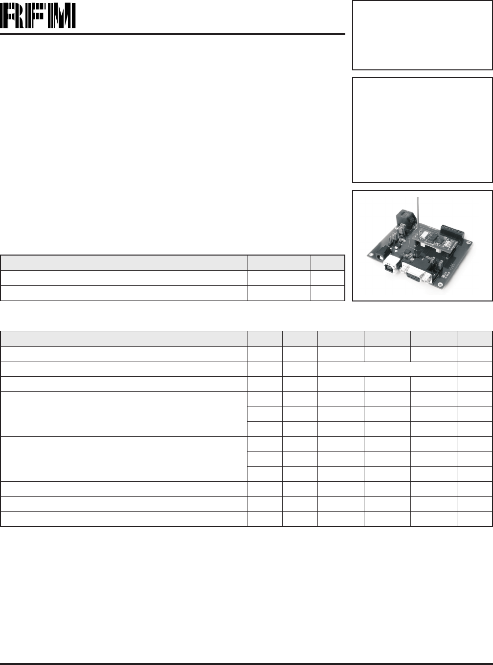
The CX2200 is a 916.5 MHz transceiver assembly designed for base station and router applications
in wireless industrial sensor networks. The communications range of the CX2200 in an “open field”
environment is typically 200 meters/hop. The CX2200 combines RFM’s very low-current ASH radio
technology with low-power microcontroller technology to achieve long battery life. The CX2200 is
compatible with RFM’s miniMESHTM network protocol, which provides add-on “plug-and-play”
multicast mesh network routing. The CX2200 transceiver assembly is certified for operation under
FCC 15.249 regulations.
•Base Station or Router Capability
•Compatible with RFM miniMESHTM Network Protocol
•3 V, Very Low Current Operation
•Ready-to-Use Assembly
2
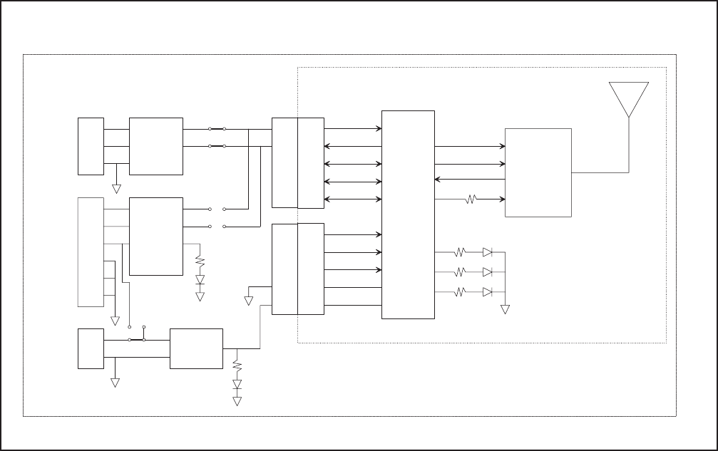
Theory of Operation
The major components of the CX2200 transceiver as-
sembly include the CM2200 transceiver module and
the CI2200 interface module. The CM2200 includes a
TR1000 ASH transceiver and a Microchip 16LF876A
microcontroller. The TR1000 operates on a frequency
of 916.5 MHz, at a nominal output power of 0.5 mW.
The CM2200 includes an insulated wire antenna,
which should be set straight and perpendicular to the
CM2200 circuit board. The CM2200 also includes
three LEDs that indicate the transceiver’s operating
modes.
The CI2200 provides a choice of RS232 or USB to in-
terface to a host computer. USB drivers for various
host computer operating systems can be obtained at
www.silabs.com (CP2101). The CI2200 also provides
regulated 3 Vdc for operating its circuitry and the
CM2200 transceiver module. The positions of the
set-up jumper blocks for RS232 operation are shown
in Figure 2, and the positions of the set-up jumper
blocks for USB operation are shown in Figure 3.
RS232 operation requires external power, which is in-
put on connector J4. The CX2200 is powered directly
from the USB connector when using the USB inter-
face. There are two LEDs on the CI2200 interface
module. LED D1 indicates that regulated 3 Vdc is
present, and the LED D2 indicates an active USB
connection.
The CX2200 is compatible with RFM’s miniMESHTM
network protocol, which provides add-on “plug-and-
play” multicast mesh network routing to improve com-
munication range and robustness.
FCC Labels and Notices
This device complies with Part 15 of the FCC rules.
Operation is subject to the following two conditions:
(1) this device may not cause harmful interference,
and (2) this device must accept any interference re-
ceived, including interference that may cause unde-
sired operation.
A clearly visible label is required on the outside of the
user’s (OEM) enclosure stating that this product con-
tains a CX2200 transceiver assembly, FCC ID: TE6-
CX2200.
WARNING: This device operates under Part 15 of the
FCC rules. Any modification to this device, not ex-
pressly authorized by RF Monolithics, Inc., may void
the user’s authority to operate this device.
C X2200 B lock D iagram
TXM O D
CNTRL0
CNTRL1
RX DATA ASH
Transceiver
Micro-
Controller
LE D 1
LE D 2
LE D 3
J1-1
J1-2
J1-3
J1-4
J1-5
E1-1
E1-2
E1-3
E1-4
E1-5
J13-1
J13-2
J13-3
J13-4
J13-5
J12-1
J12-2
J12-3
J12-4
J12-5
RXD
TXD
ADIO 0
ADIO 1
ADIO 2
VDD
GND
PG C
PG D
VPP
RS232
C onverter
J2-3
J2-2
J2-5
USB
to
Serial
C onverter
J5-2
J5-3
J5-1
J5-4
J5-5
J5-6
D-
D+
VBUS
RX
TX
GND
3 V
Regulator
J4-1
J4-2
USB
LE D
PW R
LE D
RS232
C onnector
USB
C onnector
Pow er
C onnector
C M 2200
C I2200
Figure 1

Pin Name Description
J2-2 TXD This pin is the RS232 serial output. Data from this pin is transmitted at 19.2 kb/s, using 8 data bits, no parity,
and one stop bit. This pin is inactive in the router mode.
J2-3 RXD This pin is the RS232 serial input. Data to this pin must be sent at 19.2 kb/s, using 8 data bits, no parity, and
one stop bit. This pin is inactive in the router mode.
J2-5 GND This is the RS232 ground.
J5-1 VBUS This pin is USB power.
J5-2 D- This pin is USB D-.
J5-3 D+ This pin is USB D+
J5-4 GND This pin is USB ground.
J5-5 GND This pin is USB ground.
J5-6 GND This pin is USB ground.
J4-1 VIN This pin is the power supply input. The minimum input voltage to this pin is 3.1 V, and the maximum input to
this pin is 14.0 V.
J4-2 GND This pin is power supply ground.
3
Pin Descriptions
4
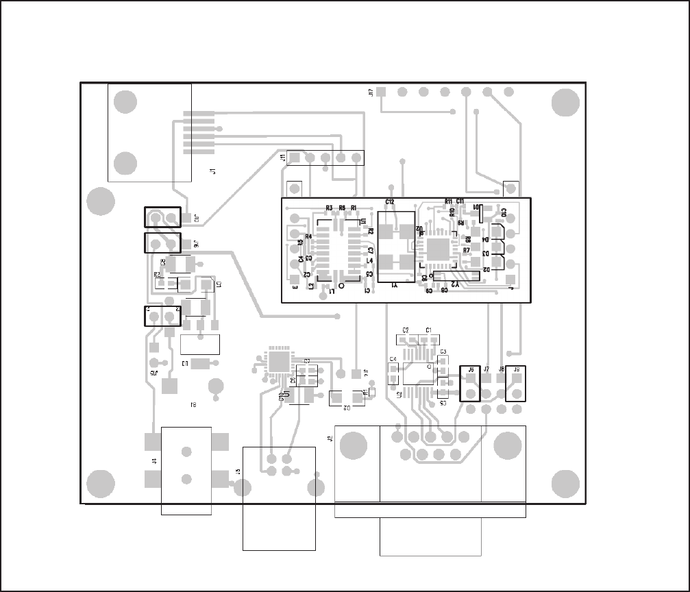
C X 2200 Transceiver A ssem bly - R S232 S et U p
P0W ER
IN P U T
U SB R S232
Figure 2
5
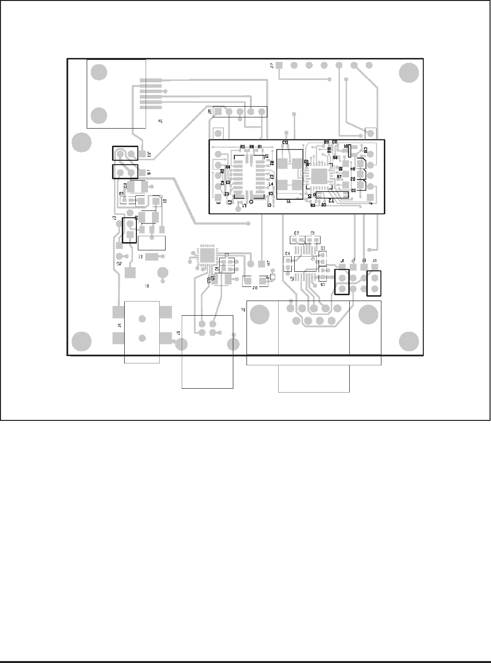
C X 2200 Transceiver A ssem bly - U S B S et U p
P0W ER
IN P U T
U SB R S232
Figure 3
Note: Specifications subject to change without notice.
file: CX2200b.vp, 2005.10.18 rev