Murata Electronics North America DRWLS1273L DR-WLS1273L-102 User Manual
Murata Electronics North America DR-WLS1273L-102
User Manual
Preliminary and RFM Confidential
www.RFM.com Technical support +1.972.448.3700 Page 1 of 31
© 2012 by RF Monolithics, Inc. E-mail: tech_sup@rfm.com DR-WLS1273L-102 Data Sheet - 12/13/12
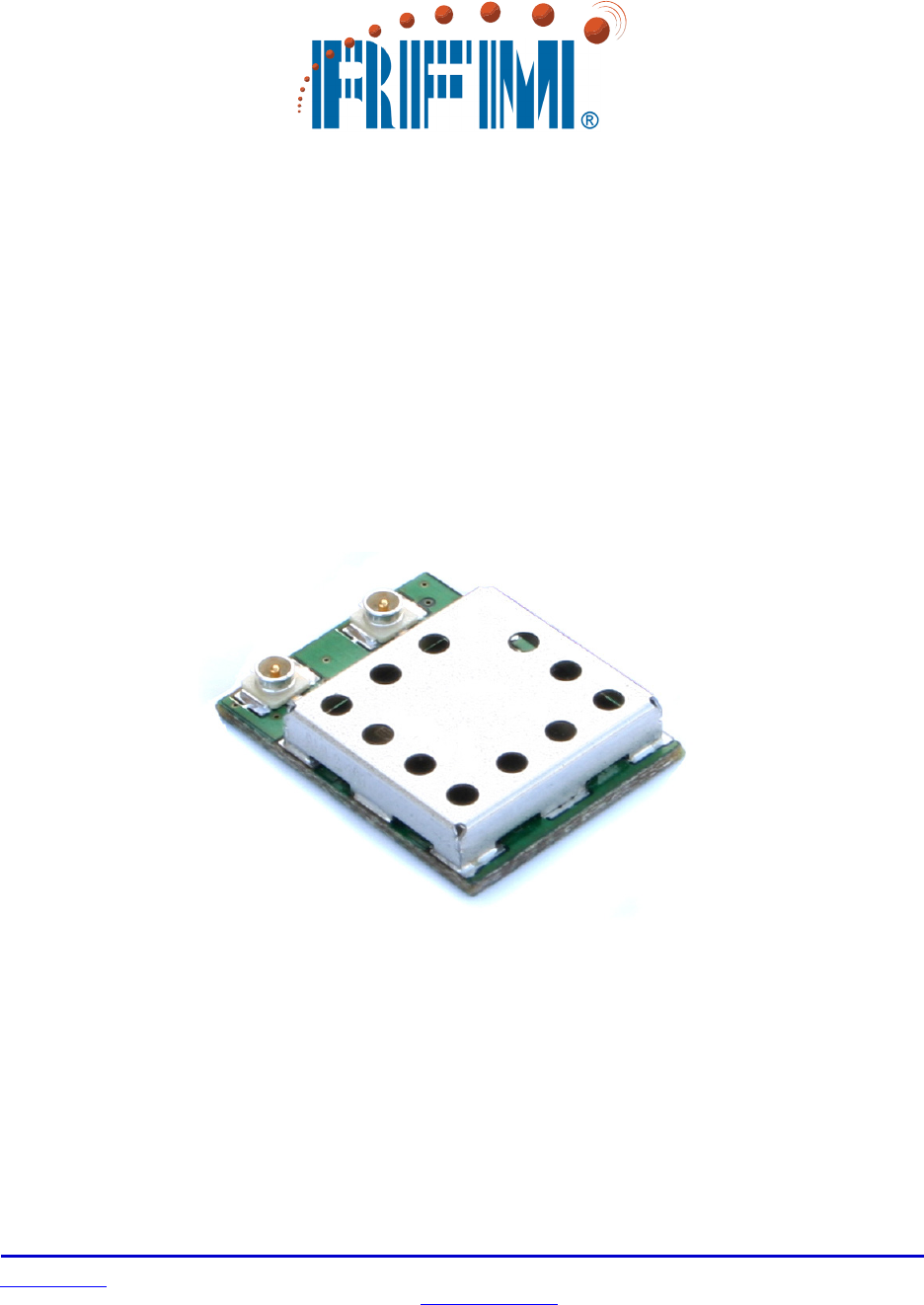
DR-WLS1273L-102
FCC/ETSI/IC Certified
WLAN/Bluetooth
Multifunction Module
Data Sheet

Preliminary and RFM Confidential
www.RFM.com Technical support +1.972.448.3700 Page 2 of 31
© 2012 by RF Monolithics, Inc. E-mail: tech_sup@rfm.com DR-WLS1273L-102 Data Sheet - 12/13/12
Scope
This specification applies to the IEEE802.11a/b/g/n WLAN and Bluetooth 4.0 standards.
Interfaces
WLAN: 4-bit SDIO
Bluetooth: UART, PCM
IC and Firmware
WLAN/BT RF/BB/MAC IC: TI WL1273L PG 3.1
Front-end IC for WL1273L: TriQuint TQP6M9002 ES1.8
Clocks and Compliance
Sleep Clock: External 32.768 kHz oscillator required
RoHS: This module is compliant with the RoHS directive
Bluetooth: Qualified Design Listing: B017989
Certifications FCC, ETSI and Industry Canada
For mobile operating conditions (greater than 20 cm to the body) - This equipment complies with FCC
radiation exposure limits set forth for an uncontrolled environment. This equipment should be installed
and operated with minimum distance 20 cm between the radiator and your body. This transmitter must
not be co-located or operating in conjunction with any other antenna or transmitter.
For portable operating conditions (less than 20 cm to the body) - This equipment complies with FCC radi-
ation exposure limits set forth for an uncontrolled environment. This equipment may operate in direct con-
tact with the body of the user under normal operating conditions. This transmitter must not be co-located
or operating in conjunction with any other antenna or transmitter.
Certification testing conducted with Antenna Factor ANT-RAF-RPS 2.4/5 GHz antenna, RSMA connector.
Part Numbers
Module: DR-WLS1273L-102
Preliminary and RFM Confidential
www.RFM.com Technical support +1.972.448.3700 Page 3 of 31
© 2012 by RF Monolithics, Inc. E-mail: tech_sup@rfm.com DR-WLS1273L-102 Data Sheet - 12/13/12
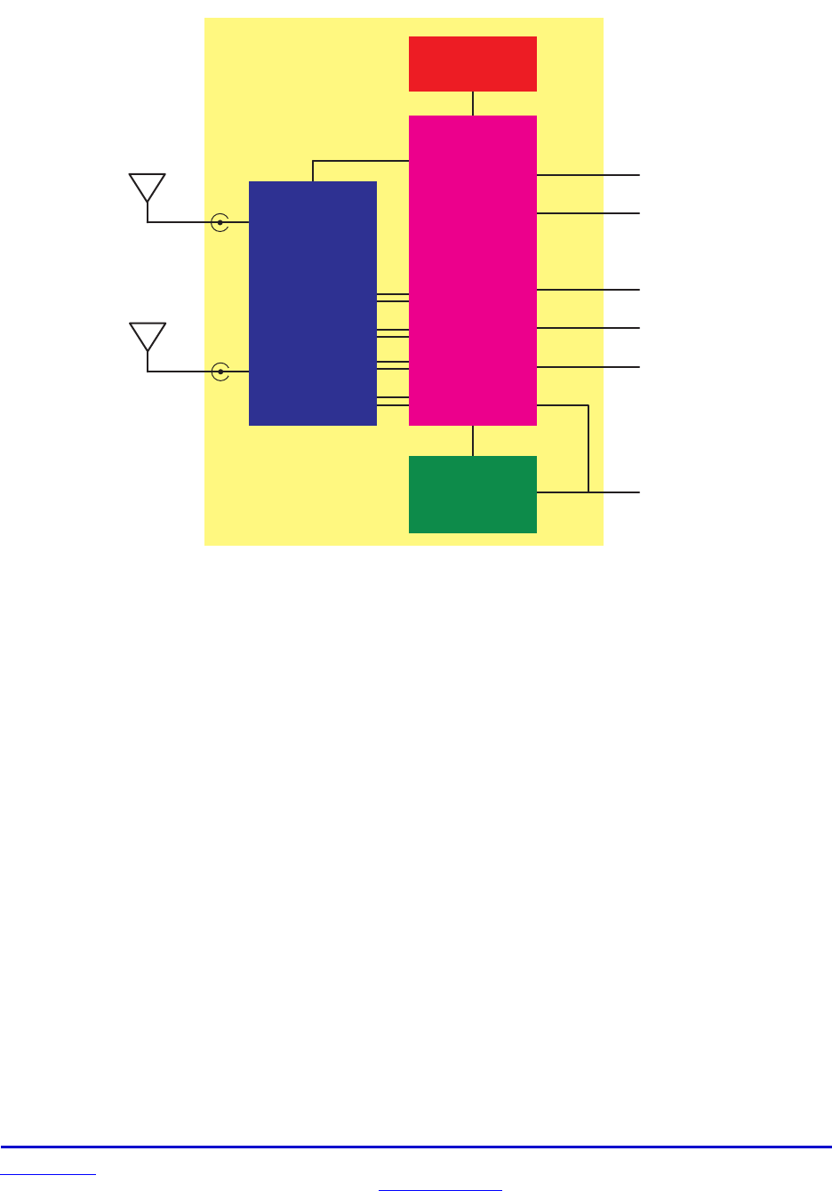
Block Diagram
2 . 4 G H z
W L A N / B T
V B A T
U A R T
P C M
S D I O
S l o w C L K
D C - D C
C o n v e r t e r
3 8 . 4 M H z
F a s t C L K
F r o n t E n d
I C a n d R F
F i l t e r i n g
5 . 8 G H z
W L A N
W L 1 2 7 3 L
V I O
DR-WLS1273L-102 WLAN Features
• WLAN MAC baseband processor and RF transceiver which are IEEE802.11a/b/g and IEEE802.11n
PICS compliant
• Optimized for ultra-low current consumption in all operating modes
• Accepts 19.2, 26, 38.4 or 52 MHz reference clock inputs for easy integration into cellular handsets, etc.
• IEEE Standard 802.11d, e, h, i, k, r, PICS compliant
• Support for Cisco Client eXtensions (CCX) standard
• Serial debug interface
• Support for Secure Digital Input/Output (SDIO) host interface
• Medium Access Controller (MAC)
– Embedded ARM™ central processing unit (CPU)
– Hardware-based encryption/decryption using 64-, 128- or 256-Bit WEP, TKIP or AES keys
– Supports Wi-Fi protected access (WPA and WPA2.0) and IEEE Standard 802.11i, including
hardware accelerated Advanced Encryption Standard (AES)
– Designed to work with IEEE Std 802.1x for Virtual Private Network (VPN) solutions

Preliminary and RFM Confidential
www.RFM.com Technical support +1.972.448.3700 Page 4 of 31
© 2012 by RF Monolithics, Inc. E-mail: tech_sup@rfm.com DR-WLS1273L-102 Data Sheet - 12/13/12
• Baseband Processor
– IEEE Std 802.11n single-stream data rates (MCS0-7) and SGI support
• 2.4/5.8 GHz Radio
– Digital Radio Processor (DRP) implementation
– Integrated LNA
– Supports IEEE Std 802.11a/b/g and 802.11n
DR-WLS1273L-102 Bluetooth Features
• V4.0 + EDR, Power Class 1.5 + BLE
• Bluetooth Qualified Design Listing: B017988
• BT Enhanced Data Rates - 2 and 3 Mbps
• Enhanced UART host interface
• Very low power consumption
• On-chip Embedded radio
– Integrated 2.4 GHz RF transceiver
– All digital PLL transmitter with digitally controlled oscillator
– Near-zero IF architecture
– On-chip TX/RX switch
– Support for Class-1.5 applications
• Embedded ARM microprocessor system
– High rate four wire UART HCI (H4) and three wire UART HCI (H5)
– Automatic clock-detection mechanism
• Flexible PCM interface - full flexibility for data order, sampling and positioning
• Temperature detection and compensation mechanism ensures minimal variation in the RF performance
over the entire operating temperature range
• Low-power scan achieves paging and inquiry scans at 1/3 normal power
• Digital Radio Processor (DRP) single-ended 50 ohm I/O for easy RF interfacing
• Patch trap mechanism and reserved RAM enables easy bug fixes
• Advance Audio Interfaces and capabilities
– A2DP support
– A2DP internal loopback
– Wide-band speech support
– On board SBC encoder/decoder - offloads host for A2DP and wide-band speech processing
– Full support for Bluetooth low energy (BLE) standard. BLE can operate in parallel with standard
Bluetooth function.
WLAN Functional Blocks
The DR-WLS1273L-102 WLAN architecture includes a digital radio processor and a point-to-multipoint
baseband core function. The architecture is based on a single-processor ARM core. The device includes
on-chip peripherals to enable easy communication between a host system and the WLAN core function.

Preliminary and RFM Confidential
www.RFM.com Technical support +1.972.448.3700 Page 5 of 31
© 2012 by RF Monolithics, Inc. E-mail: tech_sup@rfm.com DR-WLS1273L-102 Data Sheet - 12/13/12
WLAN SDIO Transport Layer
SDIO is the WLAN host interface in the DR-WLS1273L-102. This interface is a standard SDIO interface
(SDIO spec Version 2.0). The DR-WLS1273L-102 SDIO also supports the following features:
• 4-bit data bus
• Functions number 0 and 2
• Multi-Block data transfer
• The SDIO interface is used for WLAN. The WLAN block uses function 2. Function 0 is used for the
common I/O area.
WLAN MAC
The DR-WLS1273L-102 MAC implements the IEEE standard 802.11 MAC sub-layer using both dedicated
hardware and embedded firmware. The MAC hardware implements real-time functions, including access
protocol management, encryption and decryption.
WLAN Baseband Processor
The DR-WLS1273L-102 baseband processor sits between the on-chip MAC and the radio. The DR-
WLS1273L-102 baseband processor implements the IEEE 802.11a/b/g/n PHY sub-layers and has been
optimized to perform well in conditions of high multipath and noise.
WLAN RF Radio
The DR-WLS1273L-102 radio is a highly integrated Digital Radio Processor (DRP) designed for
802.11a/b/g/n applications. The DR-WLS1273L-102 RF interfaces are designed for direct, “glueless” con-
nection to single-band RF front ends for 2.4 and 5.8 GHz 802.11a/b/g/n applications.
BT Functional Blocks
The DR-WLS1273L-102 BT architecture comprises a digital radio processor and a point-to-multipoint
baseband core function. The architecture is based on a single-processor ARM core. The device includes
on-chip peripherals to enable easy communication between a host system and the Bluetooth core func-
tion.
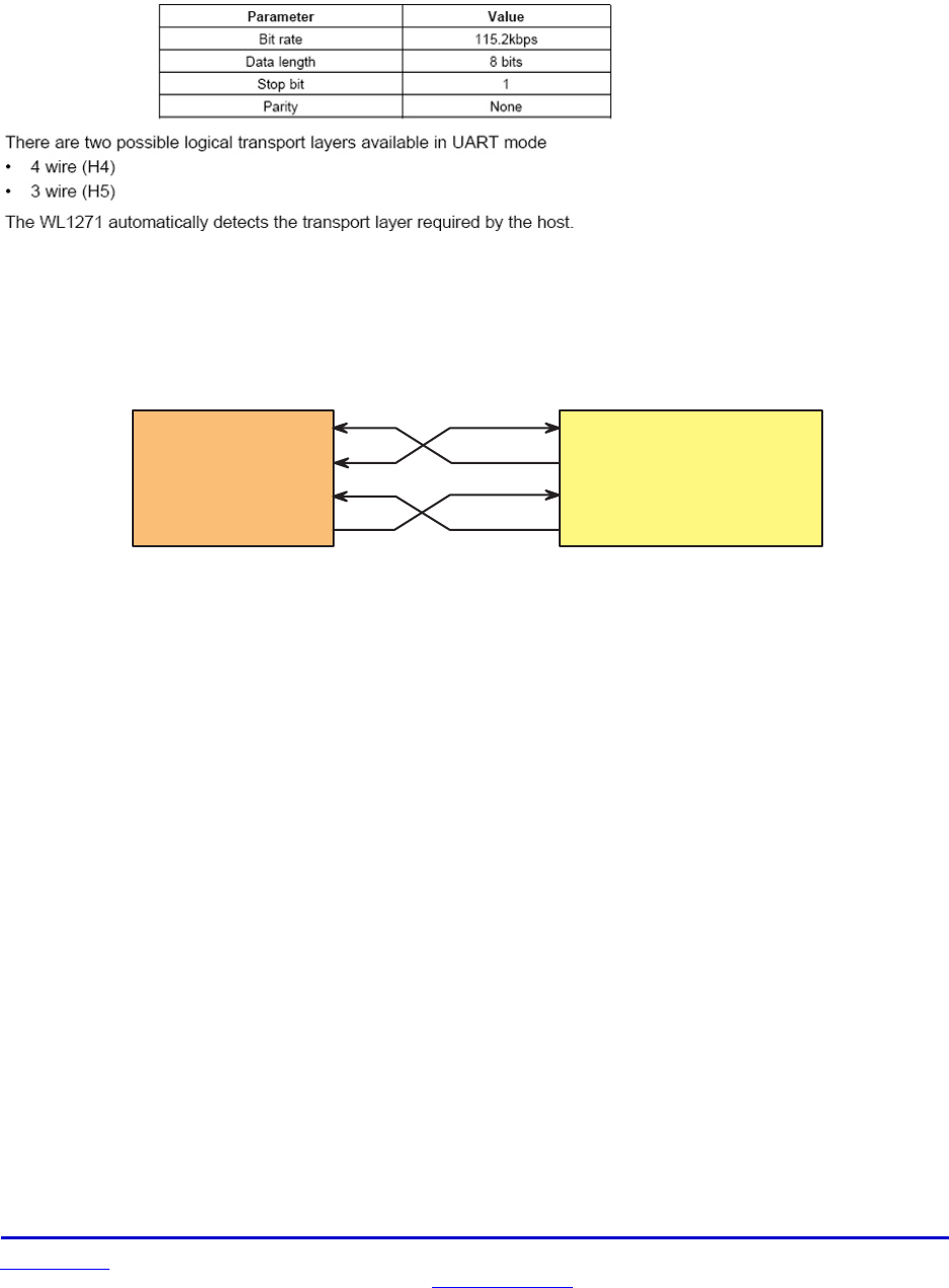
BT HCI UART Transport Layers
The DR-WLS1273L-102 incorporates one UART module dedicated to the Host Controller Interface (HCI)
transport layer. The HCI interface is used to transport commands, events, ACL and data between the
Bluetooth device and its host using HCI data packets. The DR-WLS1273L-102 supports the following HCI
transport layers, detected automatically when communication starts:
• UART transport layer - HCI four-wire (H4) and HCI three-wire (H5)
• HCI interface has a 256 byte receive buffer
The HCI UART supports most baud rates (including all PC rates) for all fast-clock frequencies - up to a
maximum of 4 Mbps. After power-up, the baud rate is set for 115.2 kbps. The maximum baud rate devia-
tion supported is -2.5%, +1.5%. The baud rate can thereafter be changed with a VS command. The DR-
WLS1273L-102 responds with a Command Complete Event (still at 115.2 kbps), after which the baud rate
change takes place. The only parameter needed is the desired baud rate. HCI hardware includes the fol-
lowing features:
Preliminary and RFM Confidential
www.RFM.com Technical support +1.972.448.3700 Page 6 of 31
© 2012 by RF Monolithics, Inc. E-mail: tech_sup@rfm.com DR-WLS1273L-102 Data Sheet - 12/13/12
• Receiver detection of break, idle, framing, FIFO overflow, and parity error conditions
• Transmitter underflow detection
• CTR/RTS hardware flow control
BT UART 4-Wire Interface - H4
The interface includes four signals: TXD, RXD, CTS and RTS. Flow control between the host and the
DR-WLS1273L-102 is byte-wise by hardware. Flow control is obtained by the following:
H O S T _ R X
H O S T T X
H O S T _ C T S
H O S T _ R T S
H C I _ R X
H C I _ T X
H C I _ C T S
H C I _ R T S
H o s t
P r o c e s s o r D R - W L S 1 2 7 3 L - 1 0 2
When the UART RX buffer asses the “flow control” threshold, it sets the UART_RTS signal high to stop
transmission from the host. When the UART_CTS signal is set high, the DR-WLS1273L-102 stops trans-
mitting on the interface. In case HCI_CTS is set high in the middle of transmitting a byte, the DR-
WLS1273L-102 finishes transmitting the byte and stops the transmission.
BT UART 3-Wire Interface - H5
This interface consists of three signals: TXD, RXD and GND:
HCI_RX Receive Data on the UART Interface
HCI_TX Transmit Data on the UART Interface
GND Ground
XON/XOFF software flow control is normally used.
The DR-WLS1273L-102 also supports a four-wire mode for H5, with RTS/CTS hardware flow control.
Since the same UART module is used for the 3- and 4-wire HCI UART interface, all features supported by
the 4-wire interface are also supported for the 3-wire interface. H5 features:
• Flow control configured with HCI_VS command, software XON/XOFF, hardware (RTS/CTS), or none
• Power management
• Configurable timers for re-transmission management
• CRC

Preliminary and RFM Confidential
www.RFM.com Technical support +1.972.448.3700 Page 7 of 31
© 2012 by RF Monolithics, Inc. E-mail: tech_sup@rfm.com DR-WLS1273L-102 Data Sheet - 12/13/12
BT Audio CODEC Interface
The CODEC interface is a fully dedicated programmable serial port that provides the logic to interface to
several kinds of PCM codecs. The interface supports:
• Two voice channels
• Master/slave modes
• Coding schemes: μ-Law, A-Law, Linear, Transparent
• Long & short frames
• Different data lengths, orders and positions
• UDI profile
• High rate PCM interface for EDR
• Enlarged interface options to support a wider variety of codecs
• PCM bus sharing
PCM Hardware Interface
The PCM interface is one implementation of the codec interface. It contains the following four lines:
• Clock - configurable direction (input or output)
• Frame Sync - configurable direction (input or output)
• Data In - Input
• Data Out - Output/Hi-Z
The DR-WLS1273L-102 device can be either the master of the interface where it generates the clock and
the frame-sync signals, or slave where it receives these two signals. The PCM interface is fully configured
by means of a VS command. For slave mode, clock input frequencies of up to 16 MHz are supported. At
clock rates above 12 MHz, the maximum data burst size is 32 bits. For master mode, the DR-WLS1273L-
102 can generate any clock frequency between 64 kHz and 4.096 MHz.
Data Format
The data format is fully configurable:
• The data length can be from 8 to 320 bits, in 1-bit increments, when working with two channels, or up to
640 bits when using 1 channel. The data length can be set independently for each channel.
• The data position within a frame is also configurable with 1-clock (bit) resolution, and can be set inde-
pendently (relative to the edge of the Frame Sync signal) for each channel.
• The Data_In and Data_Out bit order can be configured independently. For example; Data_In can start
with MSB while Data_Out starts with LSB. Each channel is separately configurable. The inverse bit order
(i.e. LSB first) is supported only for sample sizes up to 24 bits.
• The data in and data out size do not necessarily have to be the same length.
• The Data_Out line is configured as a ‘high-Z’ output between data words. Data_Out can also be set for
permanent high-Z, irrespective of data out. This allows the DR-WLS1273L-102 to be a bus slave in a mul-
ti-slave PCM environment. At power up, Data_Out is configured as high-Z.
Frame-Idle Period
The CODEC interface has the capability for frame-idle periods, where the PCM clock can “take a break”
and become ‘0’ at the end of the PCM frame, after all data has been transferred. The DR-WLS1273L-102
supports frame-idle periods both as master and slave of the PCM bus. When DR-WLS1273L-102 is the
master of the interface, the frame-idle period is configurable. There are 2 configurable parameters:
• Clk_Idle_Start - indicates the number of PCM clock cycles from the beginning of the frame till the begin-
ning of the idle period. After Clk_Idle_Start clock cycles, the clock becomes ‘0’.

Preliminary and RFM Confidential
www.RFM.com Technical support +1.972.448.3700 Page 8 of 31
© 2012 by RF Monolithics, Inc. E-mail: tech_sup@rfm.com DR-WLS1273L-102 Data Sheet - 12/13/12
• Clk_Idle_End - indicates the time from the beginning of the frame till the end of the idle period. This time
is given in multiples of PCM clock periods. The delta between Clk_Idle_Start and Clk_Idle_End is the
clock idle period, e.g., for PCM clock rate = 1 MHz, frame sync period = 10 kHz, Clk_Idle_Start = 60,
Clk_Idle_End = 90. Between each two-frame sync there are 70 clock cycles (instead of 100). The clock
idle period starts 60 clock cycles after the beginning of the frame and lasts 90-60=30 clock cycles. This
means that the idle period ends 100-90=10 clock cycles before the end of the frame. The data transmis-
sion must end prior to the beginning of the idle period.
Audio Encoding
The DR-WLS1273L-102 CODEC interface can use one of four audio coding patterns:
• A-Law (8-bit)
• m-Law (8-bit)
• Linear (8 or 16-bit)
• Transparent
Preliminary and RFM Confidential
www.RFM.com Technical support +1.972.448.3700 Page 9 of 31
© 2012 by RF Monolithics, Inc. E-mail: tech_sup@rfm.com DR-WLS1273L-102 Data Sheet - 12/13/12
Mechanical
0 . 5 7 8
( 1 4 . 7 )
0 . 7 3 5
( 1 8 . 7 )
0 . 1 0 0
( 2 . 5 )
0 . 1 3 0
( 3 . 3 )
0 . 3 6 2
( 9 . 2 )
0 . 2 5 6
( 6 . 5 )
0 . 0 4 0
( 1 . 0 )
0 . 0 3 0
( 0 . 8 )
0 . 0 3 0
( 0 . 8 )
0 . 0 4 0
( 1 . 0 )
0 . 5 0
( 1 . 3 )
0 . 0 8 0
( 2 . 0 )
0 . 0 8 0
( 2 . 0 )
0 . 1 0 5
( 2 . 7 )
0 . 0 4 1
( 1 . 0 )
0 . 0 3 0
( 0 . 8 )
0 . 0 2 8
( 0 . 7 )
0 . 5 4 2
( 2 . 1 7 )
0 . 4 8 2
( 1 2 . 2 )
0 . 0 4 3
( 1 . 1 )
D i m e n s i o n s i n i n c h e s ( m m )
Top S i d e B o t t o m
D R - W L S 1 2 7 3 L - 1 0 2 P a c k a g e D r a w i n g
1
2
1 5
1 4
5 1
2 6
2 7
2 8
4 1
4 2
4 0
5 0
1 6
V i e w f r o m T o p
0 . 1 5 ( 3 . 8 )
M a x i m u m H e i g h t
0 . 1 2 0
( 3 . 0 ) 0 . 0 8 0
( 2 . 0 )
2 . 4 G H z
5 . 8 G H z
Preliminary and RFM Confidential
www.RFM.com Technical support +1.972.448.3700 Page 10 of 31
© 2012 by RF Monolithics, Inc. E-mail: tech_sup@rfm.com DR-WLS1273L-102 Data Sheet - 12/13/12
Module Terminal Description
Num Terminal Name Type System IC Terminal Connection Description
1 PCM SYNC I/O BT WL1273L AUD_FSYNC PCM I/F
2 PCM CLK I/O BT WL1273L AUD_CLK PCM I/F
3 PCM OUT I/O BT WL1273L AUD_OUT PCM I/F
4 PCM IN I/O BT WL1273L AUD_IN PCM I/F
5 HOST WAKE I/O BT WL1273L BT_FUNC5 Host Wake Up
6 VBAT IN P SOC
WL1273L,
TPS62601 PMS_VBAT, VIN Power supply input
7 BT ENABLE I BT WL1273L BT_EN BT Enable/Reset
8 WLAN IRQ O WLAN WL1273L WLAN_IRQ WLAN interrupt request
9 NOT USED Mechanical Connection
10 NOT USED Mechanical Connection
11 NOT USED Mechanical Connection
12 NOT USED Mechanical Connection
13 NOT USED Mechanical Connection
14 WLAN TX I/O WLAN WL1273L WL_RS232_TX RS232_RX
15 WLAN RX I/O WLAN WL1273L WL_RS232_RX RS232_TX
16 WLAN EN I WLAN WL1273L WL_EN WLAN Enable/Reset
17 SDIO D2 I/O WLAN WL1273L SDIO_D2 SDIO DATA 2
18 SDIO D1 I/O WLAN WL1273L SDIO_D1 SDIO DATA 1
19 SDIO CMD I/O WLAN WL1273L SDIO_CMD SDIO CMD
20 NOT USED Mechanical Connection
21 GND SOC Ground
22 SDIO CLK I WLAN WL1273L SDIO_CLK SDIO CLK
23 UART DBG I/O WLAN WL1273L WL_UART_DBG WL_UART_DBG
24 SDIO D0 I/O WLAN WL1273L SDIO_D0 SDIO mode: DATA 0
25 NOT USED Mechanical Connection
26 SDIO D3 I/O WLAN WL1273L SDIO_D3 SDIO mode: DATA 3
27 BT UART DBG I/O BT WL1273L BT_UART_DBG
BT_UART_DBG, connect to
TP for software debug
28 NOT USED Mechanical Connection
29 NOT USED Mechanical Connection
30 SLEEP CLOCK I - WL1273L SLOWCLK SLEEP_CLK Input
31 BT WAKE I/O BT WL1273L BT_FUNC2 BT_WU/BT
32 NOT USED Mechanical Connection
33 VIO IN P SOC WL1273L VDDS Power Supply Input
34 NOT USED Mechanical Connection
Preliminary and RFM Confidential
www.RFM.com Technical support +1.972.448.3700 Page 11 of 31
© 2012 by RF Monolithics, Inc. E-mail: tech_sup@rfm.com DR-WLS1273L-102 Data Sheet - 12/13/12
Num Terminal Name Type System IC Terminal Connection Description
35 BT CTS I/O BT WL1273L HCI_CTS BT UART CTS
36 NOT USED Mechanical Connection
37 BT RTS I/O BT WL1273L HCI_RTS BT UART RTS
38 NOT USED Mechanical Connection
39 BT TX I/O BT WL1273L HCI_TX BT UART TX
40 NOT USED Mechanical Connection
41 BT RX I/O BT WL1273L HCI_RX BT UART RX
42 GND SOC Ground
43 GND SOC Ground
44 2.4 GHZ ANT I/O BT,
WLAN
RF receiver input
RF transmitter output
45 GND SOC Ground
46 GND SOC Ground
47 GND SOC Ground
48 GND SOC Ground
49 5.8 GHZ ANT I/O WLAN RF receiver input
RF transmitter output
50 GND SOC Ground
51 GND SOC Ground
Preliminary and RFM Confidential
www.RFM.com Technical support +1.972.448.3700 Page 12 of 31
© 2012 by RF Monolithics, Inc. E-mail: tech_sup@rfm.com DR-WLS1273L-102 Data Sheet - 12/13/12
Absolute Maximum Ratings
Ratings Minimum Maximum Units
Temperature -40 +85 OC
Supply Voltage VBAT -0.5 +5.5 V
VIO -0.5 +2.1 V
Operating Conditions
Specifications Minimum Typical Maximum Units
Temperature1, 2 -40 +25 +85
OC
Supply Voltage VBAT 3.0 3.6 4.2 V
VIO3 1.70 1.80 1.90 V
Digital I/O Requirements
Specifications Symbol Minimum Maximum Units
Logic High Input Voltage VIH 0.65 * VIO VIO V
Logic Low Input Voltage VIL 0 0.35 * VIO V
Logic High Output Voltage
@ 4.00 mA
VOH
VIO - 0.450 VIO
V @ 1.00 mA VIO - 0.112 VIO
@ 0.30 mA VIO - 0.033 VIO
Logic Low Output Voltage
@ 4.00 mA
VOL
0 0.450
V @ 1.00 mA 0 0.112
@ 0.09 mA 0 0.01
Input Transition Time TR/TF
from 10% to 90%4 CL < 50 fF TR/TF 0 25 ps
Output Rise Time TR
from 10% to 90%4 CL < 25 pF TR - 5.3 ns
Output Fall Time TF
from 90% to 10%4 CL < 25 pF TF - 4.9 ns
Notes:
1. The device can be reliably operated for 5,000 active WLAN hours cumulative at T ambient of 85 °C.
2. BIP (calibration) must be run to achieve full power output when temperatures changes more than 20 °C
from the last BIP
3. Minimum ramp time for IO power supply is 100 µs
4. Applies to all digital lines except SDIO, UART, PCM and slow clock lines.

Preliminary and RFM Confidential
www.RFM.com Technical support +1.972.448.3700 Page 13 of 31
© 2012 by RF Monolithics, Inc. E-mail: tech_sup@rfm.com DR-WLS1273L-102 Data Sheet - 12/13/12
External Slow Clock Requirements
Specifications1 Minimum Typical Maximum Units
Slow Clock Frequency 32.768 kHz
Slow Clock Accuracy - - ±150 ppm
Clock Transition Time, Tr/Tf 10 to 90% - - 100 ns
Clock Duty Cycle 15 50 70 %
Input Voltage Limits, Square
Wave, DC-coupled
VIH 0.65 * VIO - VIO
V
VIL 0 - 0.35 * VIO
Input Impedance 1 - - M
Input Capacitance - - 5 pF
Rise and Fall Time - - 100 ns
Phase Noise @ 1 kHz offset - - -125 dBc/Hz
Jitter, Integrated over 300 to 15000 Hz - - 1 Hz
1. The slow digital clock is a fail-safe input.
Preliminary and RFM Confidential
www.RFM.com Technical support +1.972.448.3700 Page 14 of 31
© 2012 by RF Monolithics, Inc. E-mail: tech_sup@rfm.com DR-WLS1273L-102 Data Sheet - 12/13/12
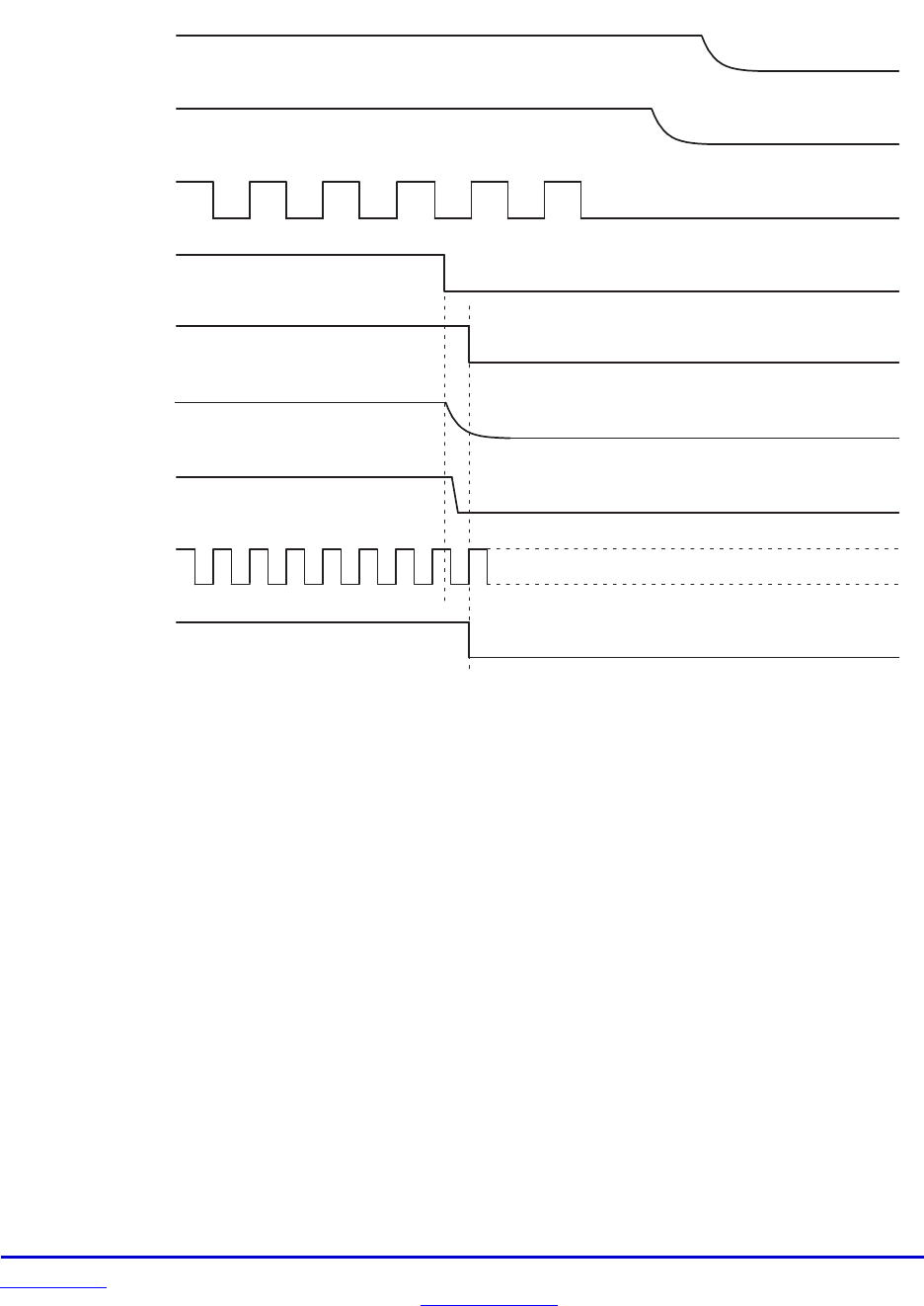
WLAN Power-up Sequence
V I O , 1 . 8 V
V B A T , 2 . 3 t o 5 . 5 V
T 1 T 2
T
W A K E U P
< 1 0 0 µ s
S L O W C L K
W L _ E N
D C _ R E Q
D C 2 D C , 1 . 8 V
C L K _ R E Q
S D I O C L K
W L A N _ I R Q
F
R E F
The following sequence describes device power up from shutdown. Only the WLAN Core is enabled; the BT core is disabled.
1. No signals are allowed on the IO pins if no IO power supplied, because the IOs are not fail-safe. Exceptions are CLQ_REQ,
SLEEP_CLK, XTALP, and PCM_xxx, which are fail-safe and can tolerate external voltages with no VIO and DC2DC.
2. VBAT,VIO and SLEEP_CLK must be available before WLAN ENABLE.
3. TWAKE-UP = T1+T2. The duration of T1 is the time from WLAN ENABLE high until FREF is valid (55 ms typical).
The duration of T2 depends on:
Operating system
Host enumeration for the SDIO
PLL configuration
Firmware download
Releasing the core from reset
Firmware initialization
Preliminary and RFM Confidential
www.RFM.com Technical support +1.972.448.3700 Page 15 of 31
© 2012 by RF Monolithics, Inc. E-mail: tech_sup@rfm.com DR-WLS1273L-102 Data Sheet - 12/13/12
WLAN Power-down Sequence
V B A T , 2 . 3 t o 5 . 5 V
V I O , 1 . 8 V
S L O W C L K
W L _ E N
D C _ R E Q
D C 2 D C , 1 . 8 V
C L K _ R E Q
S D I O C L K
W L A N _ I R Q
1. DC_REQ will go low only if WLAN is the only core working. Otherwise if the BT core is working, it will stay high.
2. CLK_REQ will go low only if WLAN is the only core working. Otherwise if the BT core is working and using the FREF it will stay
high.
3. If WLAN is the only core that is operating, WLAN ENABLE must remain de-asserted for at least 64 µs before it is re-asserted.
Preliminary and RFM Confidential
www.RFM.com Technical support +1.972.448.3700 Page 16 of 31
© 2012 by RF Monolithics, Inc. E-mail: tech_sup@rfm.com DR-WLS1273L-102 Data Sheet - 12/13/12
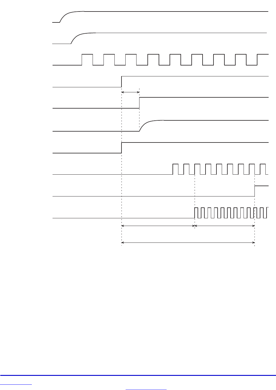
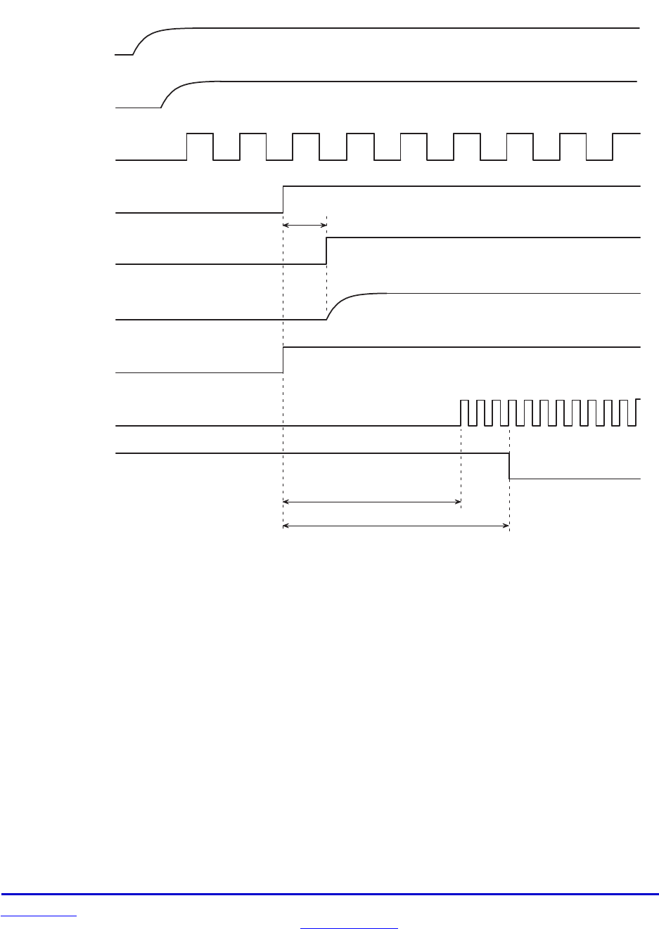
Bluetooth Power-up Sequence
V B A T
T 1
T
W A K E U P
< 1 0 0 µ s
V I O
S L E E P C L O C K
B T _ R E S E T X
D C _ R E Q
( i n t e r n a l )
DC2DC
( 1 . 8 V )
C L K _ R E Q
F
R E F
U A R T _ R T S
The following sequence describes device power-up from shutdown. Only the BT core is enabled; the WLAN
are disabled.
1. No signals are allowed on the IO pins if no IO power supplied, because the IOs are not failsafe. Exceptions are CLK_REQ,
SLEEP_CLK, XTALP and PCM_xxx, which are failsafe and can tolerate external voltages with no VIO and DC2DC.
2. VIO and SLEEP_CLK must be stable before releasing BT ENABLE (BT_RESETX).
3. Fast clock must be stable maximum 55ms after BT ENABLE goes HIGH.
4. The duration of T1 is defined as the time from BT ENABLE=high until FREF is valid (55 ms typical).
5. The duration of TWAKE-UP is defined as the time from the rising edge of BT ENABLE to the falling edge of UART_RTS.
The WL1273L indicates completion of BT power up sequence by asserting RTS low. This occurs up to 100 ms after BT ENABLE
goes high.
Preliminary and RFM Confidential
www.RFM.com Technical support +1.972.448.3700 Page 17 of 31
© 2012 by RF Monolithics, Inc. E-mail: tech_sup@rfm.com DR-WLS1273L-102 Data Sheet - 12/13/12
Bluetooth Power-down Sequence
V B A T
V I O
S L E E P C L O C K
B T _ R E S E T X
D C _ R E Q
( i n t e r n a l )
DC2DC
( 1 . 8 V )
C L K _ R E Q
U A R T _ R T S
B l u e t o o t h i n a c t i v e
The DR-WLS1273L-102 indicates completion of BT power up sequence by asserting RTS low. This occurs up to 100 ms after BT
ENABLE (BT_RESETX) goes high.
Preliminary and RFM Confidential
www.RFM.com Technical support +1.972.448.3700 Page 18 of 31
© 2012 by RF Monolithics, Inc. E-mail: tech_sup@rfm.com DR-WLS1273L-102 Data Sheet - 12/13/12
Host Interface Combination
WLAN BT
4-bit SDIO UART
All core functions support automatic host-interface recognition. The user does not need to configure it in advance.
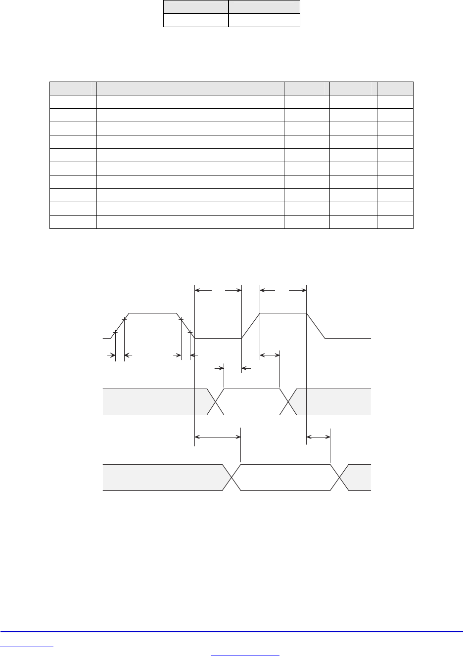
SDIO Interface Switching Characteristics, 25 pF Load Capacitance
Symbol Parameter Minimum Maximum Units
FCLOCK Clock Frequency 0 25 MHz
DC Low/High Duty Cycle 40 60 %
tWL Pulse Duration, Clock Low 10 ns
tWH Pulse Duration, Clock High 10 ns
tTLH Clock Rise Time 4.3 ns
tTHL Clock Fall Time 3.5 ns
tISU Set-up Time, Input Valid before Clock 5 ns
tIH Hold Time, Input Valid after Clock 5 ns
tODLY1 Delay Time, Clock Falling Edge to Output Valid 0 14 ns
tODLY2 Delay Time, Clock Falling Edge to Output Invalid 0 14 ns
SDIO Timing
C l o c k
I n p u t
O u t p u t
V
I H
V
I L
V
O H
V
O L
V
I L
V
I H
t
T L H
t
T H L
t
W L
t
W H
t
I H
t
I S U
t
O D L Y 2
t
O D L Y 1
0.2
0.7
Preliminary and RFM Confidential
www.RFM.com Technical support +1.972.448.3700 Page 19 of 31
© 2012 by RF Monolithics, Inc. E-mail: tech_sup@rfm.com DR-WLS1273L-102 Data Sheet - 12/13/12
SDIO Interface Read
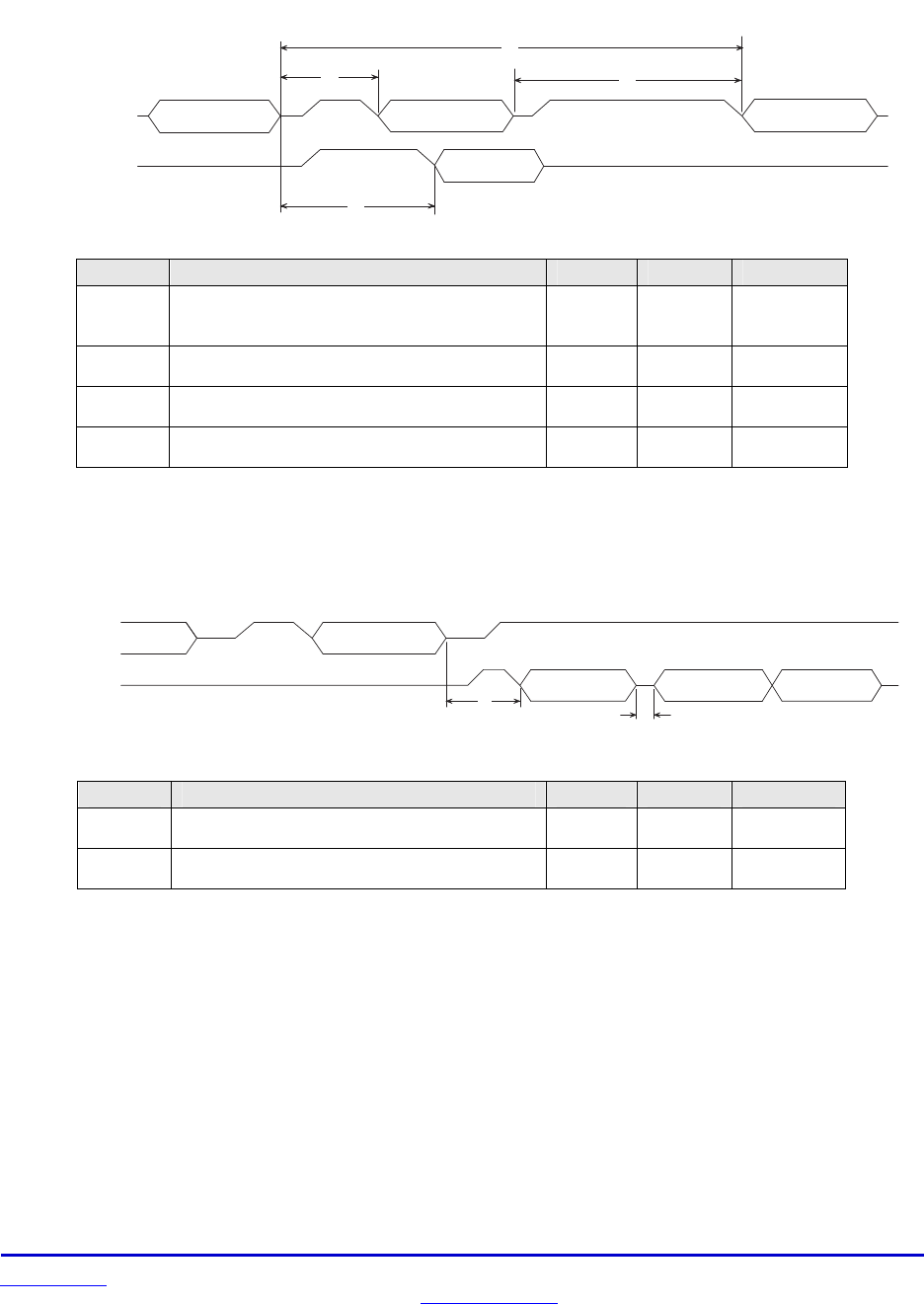
R e a d C o m m a n d C a r d R e s p o n s e C o m m a n d
R e a d
t
R C
t
C C
t
A C
t
C R
C M D
( I n p u t / O u t p u t )
S D 0 - S D 3
( I n p u t / O u t p u t )
Symbol Parameter Minimum Maximum Units
tCR
Delay Time, Assign Relative Address or
Data Transfer Mode; Read command CMD invalid
to card response CMD valid
2 64 Clock Cycles
tCC Delay Time, CMD command invalid to
CMD command valid 8 - Clock Cycles
tRC Delay Time, CMD response invalid to
CMD command valid 8 - Clock Cycles
tAC Access Time, CMD command invalid to
SD0-SD3 read data valid 8 - Clock Cycles
SDIO Interface Write
C M D
( I n p u t / O u t p u t )
S D 0 - S D 3
( I n p u t / O u t p u t )
C a r d R e s p o n s e
W r i t e C R C S t a t u s B u s y
t
d 1
t
d 2
Symbol Parameter Minimum Maximum Units
Td1 Delay Time, CMD Card Response Invalid to
SD0-SD3 Write Data Valid
2 - Clock Cycles
Td2 Delay Time, SD0-SD3 Write Data Invalid to
CRC Status Valid
2 2 Clock Cycles
Preliminary and RFM Confidential
www.RFM.com Technical support +1.972.448.3700 Page 20 of 31
© 2012 by RF Monolithics, Inc. E-mail: tech_sup@rfm.com DR-WLS1273L-102 Data Sheet - 12/13/12
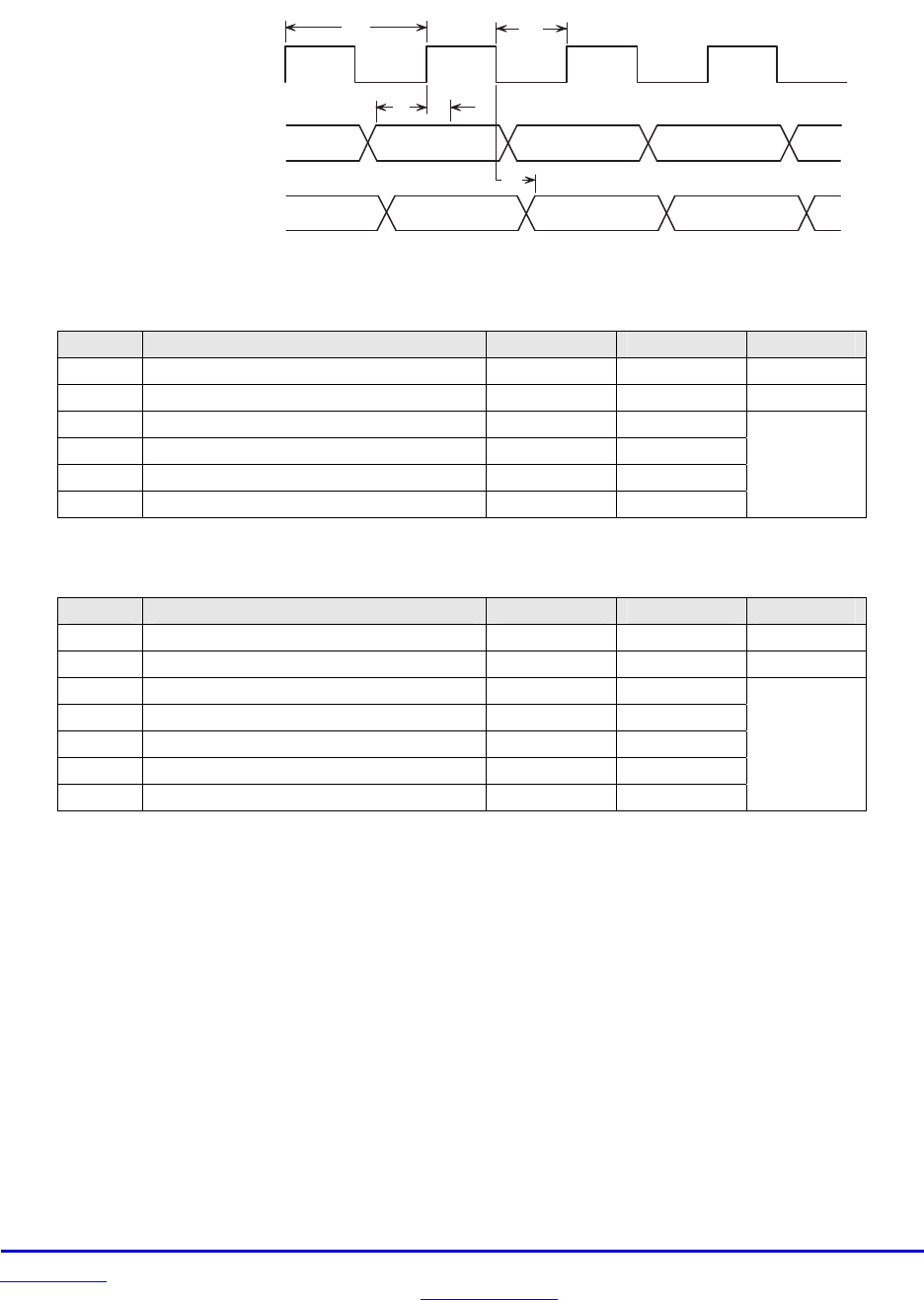
BT Audio CODEC/PCM Interface Switching Characteristics
T
c l k
T
W
t
o p
t
i s
t
i h
A U D _ C L K
A U D _ I N / F S Y N C _ I N
A U D _ O U T / F S Y N C _ O U T
PCM Master
Symbol Parameter Minimum Maximum Units
TCLK Clock Period 166.7 (6 MHz) 15625 (64 kHz) ns
TW High/Low Pulse Width 50% of TCLK
tis AUD_IN Setup Time 25
ns
tih AUD_IN Hold Time 0
top AUD_OUT Propagation Time, 40 pF Load 0 10
top FSYNC_OUT Propagation Time, 40 pF Load 0 10
PCM Slave
Symbol Parameter Minimum Maximum Units
TCLK Clock Period 62.5 (16 MHz) ns
TW High/Low Pulse Width 40% of TCLK
tis AUD_IN Setup Time 8
ns
tih AUD_IN Hold Time 0
tis FSYNC_IN Setup Time 8
tih FSYNC_IN Hold Time 0
top AUD_OUT Propagation Time, 40 pF Load 0 21
Preliminary and RFM Confidential
www.RFM.com Technical support +1.972.448.3700 Page 21 of 31
© 2012 by RF Monolithics, Inc. E-mail: tech_sup@rfm.com DR-WLS1273L-102 Data Sheet - 12/13/12
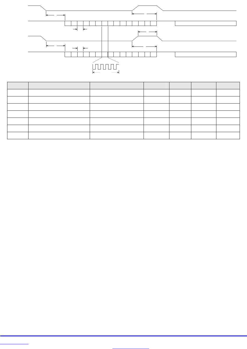
UART Interface Timing
H C I _ R T S
H C I _ R X
H C I _ C T S
H C I _ T X
1 0 b i t s
t1t2
t6
t5
t3t7
t4
Symbol Parameter Condition Minimum Typical Maximum Units
BR Baud Rate Most Standard Rates 37.5 - 4000 kbps
t5, t7 Baud Rate Accuracy Receive/Transmit -2.5 - 1.5 %
t3 CTS Low to TX_DATA 0 2 - µs
t4 CTS High to TX_DATA Hardware Flow Control - - 1 byte
t6 CTS High Pulse Width 1 - - bit
t1 RTS Low to RX_DATA ON 0 2 - µs
t2 RTS High to RX_DATA OFF Interrupt set to 1/4 FIFO - - 16 byte
DR-WLS1273L-102 IRQ Operation
1. The default state of the WLAN_IRQ prior to firmware initialization is 0.
2. During firmware initialization, the WLAN_IRQ is configured by the SDIO module; a WLAN_IRQ
changes its state to 1
3. A WLAN firmware interrupt is handled as follows:
(a) The WLAN firmware creates an Interrupt-to-Host, indicated by a 1-to-0 transition on the WLAN_IRQ
line (host must be configured as active-low or falling-edge detect).
(b) After the host is available, depending on the interrupt priority and other host tasks, it masks the
firmware interrupt. The WLAN_IRQ line returns to 1 (0-to-1 transition on the WLAN_IRQ line).
(c) The host reads the internal register status to determine the interrupt sources - the register is cleared
after the read
(d) The host processes in sequence all the interrupts read from this register
(e) The host unmasks the firmware interrupts.
4. The host is ready to receive another interrupt from the WLAN device.
DR-WLS1273L-102 BT Function Low Power Mode Protocols
The DR-WLS1273L-102 includes a mechanism that handles the transition between operating mode and
deep sleep low-power mode. The protocol is done via the UART and is known as eHCILL (enhanced HCI
Low Level) power management protocol. This protocol is backward compatible with the
BRF6150/BRF6300 /BRF6350/WL1273 HCILL Protocol, so a Host that implements the HCILL for
BRF6150/BRF6350 does not need to change anything in order to work with the DR-WLS1273L-102. The
"Enhanced" portion of the HCILL introduces changes that allow a simpler host implementation of this pro-
tocol. See BT-SW-0024 (BRF Enhanced HCILL 4 wire Power Management Protocol). In addition to the
HCILL protocol, the DR-WLS1273L-102 also supports the power management schemes inherent in the
UART H5 transport layers.
Preliminary and RFM Confidential
www.RFM.com Technical support +1.972.448.3700 Page 22 of 31
© 2012 by RF Monolithics, Inc. E-mail: tech_sup@rfm.com DR-WLS1273L-102 Data Sheet - 12/13/12
DC and RF Characteristics for IEEE 802.11b Operation, 11 Mbps, 2.4 GHz
Conditions: 25 C, VBAT=3.6 V, VIO=1.8 V, VDD_LDO_IN_CLASS1P5 connected to VBAT
System Specifications Data
Standard IEEE802.11b
Mode DSSS/CCK
Frequency, Spacing 2412 to 2462 MHz, 5 MHz
Data Rate 1, 2, 5.5, 11 Mbps
DC Specifications Minimum Typical Maximum Units
DC Current:
TX Mode - 265 350 mA
RX Mode - 100 150 mA
Sleep Mode - 89 200 µA
Transmitter Specifications Minimum Typical Maximum Units
RF Output Power 16 18 20 dBm
Spectrum Mask:
1st Sidelobes - -46 -30 dBr
2nd Sidelobes - -55 -50 dBr
Power-on and Power-off Ramp - 0.06 2.00 µs
RF Carrier Suppression - - -15 dB
Modulation Accuracy (EVM) - 7 35 %
Out-of-Band Spurious Emissions:
0.03 to 1 GHz - -96 -36 dBm
1 to 12.75 GHz - -55 -30 dBm
1.8 to 1.9 GHz - -96 -47 dBm
Receiver Specifications Minimum Typical Maximum Units
Sensitivity:
Minimum Input Level, 11 Mbps, FER 8% - -87 -76 dBm
Maximum Input Level, FER 8% -10 - - dBm
Adjacent Channel Rejection, FER 8% 35 - - dB
Preliminary and RFM Confidential
www.RFM.com Technical support +1.972.448.3700 Page 23 of 31
© 2012 by RF Monolithics, Inc. E-mail: tech_sup@rfm.com DR-WLS1273L-102 Data Sheet - 12/13/12
DC and RF Characteristics for IEEE 802.11g Operation, 54 Mbps, 2.4 GHz
Conditions: 25 C, VBAT=3.6V, VIO=1.8V, VDD_LDO_IN_CLASS1P5 is connected to VBAT
System Specifications Data
Standard IEEE802.11g
Mode OFDM
Frequency, Spacing 2412 to 2462 MHz, 5 MHz
Data Rate 6, 9, 12, 24, 36, 48, 54 Mbps
DC Specifications Minimum Typical Maximum Units
DC Current:
TX Mode - 180 270 mA
RX Mode - 100 150 mA
Sleep Mode - - 200 µA
Transmitter Specifications Minimum Typical Maximum Units
RF Output Power 11 13 15 dBm
Spectrum Mask:
at fC ±11 MHz - -31 -20 dBr
at fC ±20 MHz - -39 -28 dBr
at fC ≥ ±30 MHz - -50 -40 dBr
Constellation Error (EVM) - -34 -25 dB
Out-of-Band Spurious Emissions:
0.03 to 1 GHz - -96 -36 dBm
1 to 12.75 GHz - -58 -30 dBm
1.8 to 1.9 GHz - -96 -47 dBm
Receiver Specifications Minimum Typical Maximum Units
Sensitivity:
Minimum Input Level, 54 Mbps, PER 10% - -74 -65 dBm
Maximum Input Level, PER 10% -20 - - dBm
Adjacent Channel Rejection, 54 Mbps, PER 10% -1 - - dB
Preliminary and RFM Confidential
www.RFM.com Technical support +1.972.448.3700 Page 24 of 31
© 2012 by RF Monolithics, Inc. E-mail: tech_sup@rfm.com DR-WLS1273L-102 Data Sheet - 12/13/12
DC and RF Characteristics for IEEE 802.11a Operation, 54 Mbps, 5 GHz
Conditions: 25 deg C, VBAT=3.6 V, VIO=1.8 V, VDD_LDO_IN_CLASS1P5 is connected to VBAT
System Specifications Data
Standard IEEE802.11a
Mode OFDM
Frequency, Spacing 5180 to 5320 MHz, 20 MHz
Data Rate 6, 9, 12, 24, 36, 48, 54 Mbps
DC Specifications Minimum Typical Maximum Units
DC Current:
TX Mode - 213 270 mA
RX Mode - 100 150 mA
Transmitter Specifications Minimum Typical Maximum Units
RF Output Power 10 12 14 dBm
Spectrum Mask:
at fC ±11 MHz - -31 -20 dBr
at fC ±20 MHz - -39 -28 dBr
at fC ≥ ±30 MHz - -50 -40 dBr
Constellation Error (EVM) - -30 -25 dB
Out-of-Band Spurious Emissions:
0.03 to 1 GHz - -92 -36 dBm
1 to 12.75 GHz - -54 -30 dBm
1.8 to 1.9 GHz - -96 -47 dBm
Receiver Specifications Minimum Typical Maximum Units
Sensitivity:
Minimum Input Level, 54 Mbps, PER 10% - -72 -65 dBm
Maximum Input Level, PER 10% -30 - - dBm
Adjacent Channel Rejection, 54 Mbps, PER 10% -1 - - dB
Preliminary and RFM Confidential
www.RFM.com Technical support +1.972.448.3700 Page 25 of 31
© 2012 by RF Monolithics, Inc. E-mail: tech_sup@rfm.com DR-WLS1273L-102 Data Sheet - 12/13/12
DC and RF Characteristics for IEEE 802.11n Operation, 65 Mbps, 2.4 GHz
Conditions: 25 C, VBAT=3.6 V, VIO=1.8 V, VDD_LDO_IN_CLASS1P5 is connected to VBAT
System Specifications Data
Standard IEEE802.11n-2.4G
Mode OFDM
Frequency, Spacing 2412 to 2462 MHz, 5 MHz
Data Rate 6.5, 13, 19.5, 26, 39, 52, 58.5, 65 Mbps
DC Specifications Minimum Typical Maximum Units
DC Current:
TX Mode - 180 250 mA
RX Mode - 100 150 mA
Transmitter Specifications Minimum Typical Maximum Units
RF Output Power 10 12 14 dBm
Spectrum Mask:
at fC ±11 MHz - -30 -20 dBr
at fC ±20 MHz - -33 -28 dBr
at fC ≥ ±30 MHz - -49 -45 dBr
Constellation Error (EVM) - - -28 dB
Out-of-Band Spurious Emissions:
0.03 to 1 GHz - -95 -36 dBm
1 to 12.75 GHz - -71 -30 dBm
1.8 to 1.9 GHz - -96 -47 dBm
Receiver Specifications Minimum Typical Maximum Units
Sensitivity:
Minimum Input Level, 65 Mbps, PER 10% - -70 -64 dBm
Maximum Input Level, PER 10% -20 - - dBm
Preliminary and RFM Confidential
www.RFM.com Technical support +1.972.448.3700 Page 26 of 31
© 2012 by RF Monolithics, Inc. E-mail: tech_sup@rfm.com DR-WLS1273L-102 Data Sheet - 12/13/12
DC and RF Characteristics for IEEE 802.11n Operation, 65 Mbps, 5 GHz
Conditions: 25 C, VBAT=3.6 V, VIO=1.8 V, VDD_LDO_IN_CLASS1P5 is connected to VBAT
System Specifications Data
Specification IEEE802.11n-5G
Mode OFDM
Frequency, Spacing 5180 to 5320 MHz, 5 MHz
Data Rate 6.5, 13, 19.5, 26, 39, 52, 58.5, 65 Mbps
DC Specifications Minimum Typical Maximum Units
DC Current:
TX Mode - 225 270 mA
RX Mode - 107 150 mA
Transmitter Specifications Minimum Typical Maximum Units
RF Output Power 10 12 14 dBm
Spectrum Mask:
at fC ±11 MHz - -30 -20 dBr
at fC ±20 MHz - -34 -28 dBr
at fC ≥ ±30 MHz - -49 -45 dBr
Constellation Error (EVM) - TBD TBD dB
Out-of-Band Spurious Emissions:
0.03 to 1 GHz - -96 -36 dBm
1 to 12.75 GHz - -55 -30 dBm
1.8 to 1.9 GHz - -96 -47 dBm
Receiver Specifications Minimum Typical Maximum Units
Sensitivity:
Minimum Input Level, 65 Mbps, PER 10% - -67 -64 dBm
Maximum Input Level, PER 10% -30 - - dBm
Preliminary and RFM Confidential
www.RFM.com Technical support +1.972.448.3700 Page 27 of 31
© 2012 by RF Monolithics, Inc. E-mail: tech_sup@rfm.com DR-WLS1273L-102 Data Sheet - 12/13/12
DC and RF Characteristics for Bluetooth Operation, 2.4 GHz
Conditions: 25 C, VBAT=3.6 V, VIO=1.8 V, VDD_LDO_IN_CLASS1P5 is connected to VBAT
System Specifications Data
Bluetooth Standard Version 4.0
Channel Spacing 1 MHz
Number of RF Channels 79
Power Class 1.5
Operating Mode
Frequency hopping spread spectrum, pseudorandom hopping pattern,
time division multiple access on transmit or receive,
frequency hop after each RX/TX cycle
DC Specifications Minimum Typical Maximum Units
DC Current:
DH1 Packet, 50% RX/TX Slot Duty Cycle - 38 60 mA
DH3 Packet, 50% RX/TX Slot Duty Cycle - 45 60 mA
DH5 Packet, 50% RX/TX Slot Duty Cycle - 48 60 mA
Transmitter Specifications Minimum Typical Maximum Units
RF Output Power 4.5 8.5 - dBm
Frequency Range, RX/TX 2400 to 2483.5 MHz
-20 dB Bandwidth - 0.925 1 MHz
Adjacent Channel Power1:
M - N = 2 - -45 -20 dBm
M - N ≥ 3 - -46.5 -40 dBm
Modulation Characteristics:
Modulation f1 average 140 160 175 kHz
Modulation f2 average 115 132 - kHz
Modulation f2 average / f1 average 0.8 0.9 - -
Initial Frequency Tolerance -75 - +75 kHz
Frequency Drift:
1 Slot -25 +11 +25 kHz
3 Slots -40 +11.5 +40 kHz
5 Slots -40 +11.5 +40 kHz
Maximum Frequency Drift Rate -20 ±5 +20 kHz/50 µs
Out-of-Band Spurious Emissions:
0.03 to 1 GHz - -64 -36 dBm
1 to 12.75 GHz - -47 -30 dBm
1.8 to 1.9 GHz - - -47 dBm
5.15 to 5.30 GHz - - -47 dBm
ERD Relative Power -4 -0.2 1 dB
EDR Carrier Frequency Stability and
Modulation Accuracy, /4-DQPSK:
-75 - +75 kHz
-10 - +10 kHz
-75 - +75 kHz
RMS DEVM - 4 20 %
99% DEVM - - 30 %
Peak DEVM - 9 35 %
Preliminary and RFM Confidential
www.RFM.com Technical support +1.972.448.3700 Page 28 of 31
© 2012 by RF Monolithics, Inc. E-mail: tech_sup@rfm.com DR-WLS1273L-102 Data Sheet - 12/13/12
Transmitter Specifications (continued) Minimum Typical Maximum Units
EDR Carrier Frequency Stability and
Modulation Accuracy, 8DQPSK:
-75 - +75 kHz
-10 - +10 kHz
-75 - +75 kHz
RMS DEVM - 4 13 %
99% DEVM - - 20 %
Peak DEVM - 11.5 25 %
Receiver Specifications Minimum Typical Maximum Units
Sensitivity, BER 0.1%:
2402 MHz - -90 -70 dBm
2441 MHz - -90 -70 dBm
2480 MHz - -90 -70 dBm
C/I Performance, BER 0.1%2:
Co-channel ratio, -60 dBm Input - 8 11 dB
1 MHz ratio, -60 dBm Input - -8 0 dB
2 MHz ratio, -60 dBm Input - -46 -30 dB
3 MHz ratio, -67 dBm Input - -49 -40 dB
Image ratio, -67 dBm Input - -26 -9 dB
Image ±1 MHz ratio, -67 dBm input - 47 -20 dB
Blocking Performance, BER 0.1%3:
30 to 2000 MHz -10 - - dBm
2000 to 2400 MHz -27 - - dBm
2500 to 3000 MHz -27 - - dBm
3000 to 12750 MHz -10 - - dBm
Intermodulation Performance, -64 dBm Input,
BER 0.1% -39 -11 - dBm
Maximum Input Level -20 - - dBm
EDR Sensitivity, BER 0.01%:
/4-DQPSK - -90 -70 dBm
8DPSK - -83.5 -70 dBm
1. Up to three spurious responses within Bluetooth limits are allowed.
2. Up to five spurious responses within Bluetooth limits are allowed.
3. Up to twenty-four spurious responses within Bluetooth limits are allowed.

Preliminary and RFM Confidential
www.RFM.com Technical support +1.972.448.3700 Page 29 of 31
© 2012 by RF Monolithics, Inc. E-mail: tech_sup@rfm.com DR-WLS1273L-102 Data Sheet - 12/13/12
Storage Conditions
This product should be stored without opening the packing in an ambient temperature range of 5 to 35 C
and humidity range from 20 to 70% RH, and be used within six months of receipt. Packing materials can
be deformed at temperatures above 40 C. If the product is not used six months or more after receipt, its
solderbility should be tested before being used. The product should be stored in non-corrosive gas. Any
excess mechanical shock such as sticking the packing materials with a sharp object or dropping the
product, etc., must be avoided in order not to damage the packing materials. This product is applicable to
MSL3, based on JEDEC Standard J-STD-020.
After the packing is opened, the product should be stored at an ambient temperature below 30 C and at
humidity level less than 60% RH. The product should be used within 168 hours. If the color of the indica-
tor in the packing has changed, the product should be baked before soldering at 125 to 130 C for 24
hours. The products should be baked on the heat-resistant tray, as the tape and reel materials are not
heat-resistant.
Handling Conditions
Use care in handling or transporting this product as excessive stress or mechanical shock can crack or
break the product. Do not touch this product with bare hands as this can result in poor solderability.
Standard PCB Design (Land Pattern and Dimensions)
All the ground terminals should be connected to the ground patterns, and unconnected terminals should
be soldered to unconnected PCB pads for mechanical strength. The best land pattern depends on the
pattern generation method, grounding method, land dimensions, land forming method of the unconnected
terminals and the PCB material and thickness. Contact RFM technical support if you have any questions
about adapting the recommend land pattern to your application specifics or before using non-standard
land dimensions, etc.
Module PCB Placement
This product can be broken by uneven forces from a worn-out chucking locating claw or a suction nozzle.
To prevent damage, be sure to follow the specifications for the maintenance of the chip placer being
used. Be aware that mechanical chucking can damage this product when used for mounting it on a PCB.
Module Soldering
Preheat so that the temperature difference T between the solder and module surface is less than
130 C. If the module is immersed in solvent after mounting, care should be taken to limit the temperature
difference to 100 C. These provisions are necessary to prevent damage due to excessive differential ex-
pansion. Contact RFM technical support if you have any questions about soldering methods or are con-
sidering other soldering conditions.
Preliminary and RFM Confidential
www.RFM.com Technical support +1.972.448.3700 Page 30 of 31
© 2012 by RF Monolithics, Inc. E-mail: tech_sup@rfm.com DR-WLS1273L-102 Data Sheet - 12/13/12
Using a Soldering Iron
A soldering iron of 18 W or less, using a ceramic heater is recommended. The soldering iron tip diameter
should be 3 mm maximum, and the tip temperature should be 350 C or less. The iron contact time at
each terminal should be limited to 3 seconds. The soldering iron should be applied to the land pattern
next to the module terminal, not directly on the module ceramic substrate.
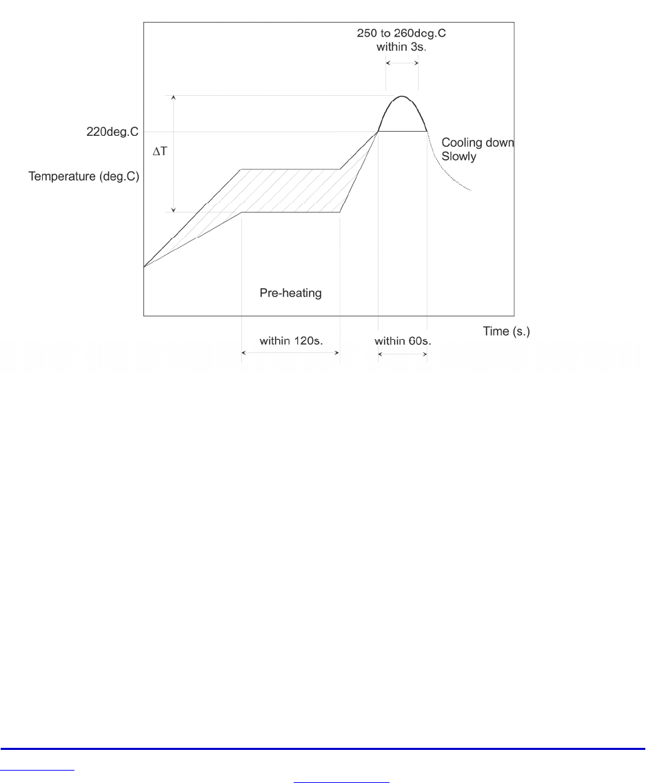
Example Reflow Soldering Profile
Use rosin flux or a weakly active flux with a chlorine content of 0.2 wt% or less.
Preliminary and RFM Confidential
www.RFM.com Technical support +1.972.448.3700 Page 31 of 31
© 2012 by RF Monolithics, Inc. E-mail: tech_sup@rfm.com DR-WLS1273L-102 Data Sheet - 12/13/12
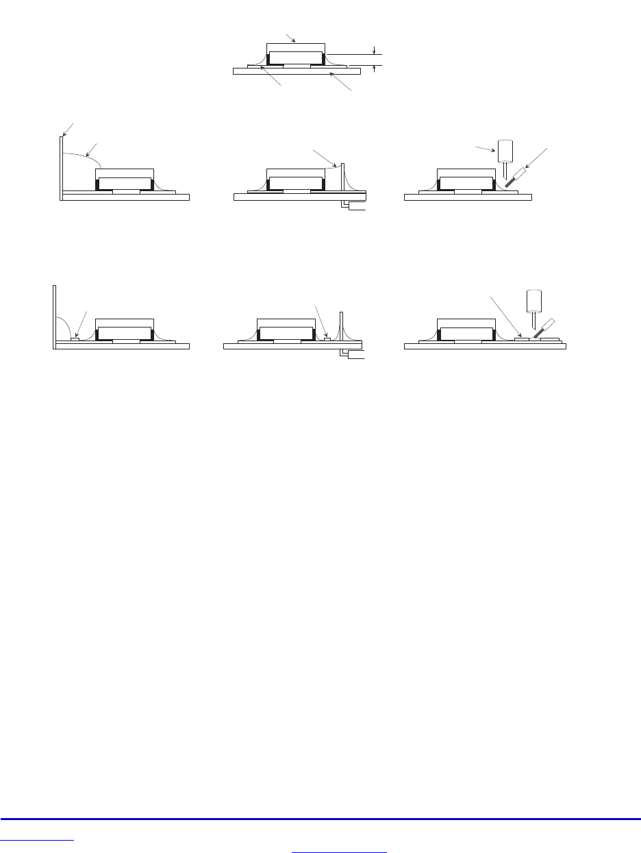
Solder Paste Amount and Assembly Standards
Ensure that solder is applied smoothly to a minimum height of 0.2 to 0.5 mm at the end surface of the
module’s external pads. If too much or little solder is applied, the mechanical strength can be insufficient.
M o d u l e
S o l d e r
F i l l e t
H e i g h t
U n a c c e p t a b l e A s s e m b l y
S a t i s f a c t o r y A s s e m b l y u s i n g S o l d e r M a s k i n g
S o l d e r W i c k i n g
f r o m W i r e o f
L e a d e d C o m p o n e n t
C h a s s i s
S o l d e r G r o u n d
W i c k i n g t o M o d u l e
S o l d e r M a s k
B l o c k s W i c k i n g
t o M o d u l e
S o l d e r M a s k
B l o c k s W i c k i n g t o
C o m p o n e n t L e a d
W i r e L e a d o f
C o m p o n e n t
M o u n t e d L a t e r
S o l d e r i n g
I r o n
P r o p e r A m o u n t o f S o l d e r P a s t e
P C B
S u b s t r a t e
P C B
L a n d
S o l d e r M a s k
Cleaning
This product is moisture sensitive and not suitable for water-based cleaning.
Operational Conditions
This product is designed to work under normal environmental conditions - ambient temperature, humidity
and pressure. If this product is used under the following circumstances, erratic operation or complete fail-
ure can occur:
Atmosphere containing a corrosive gas ( Cl2, NH3, SOx, NOx, etc.)
Atmosphere containing a combustible or volatile gas
Dusty location
Location with direct sunlight
Location subject to water splashes, high humidity or condensation
If the customer’s application could subject a module to one or more of the above conditions, consult with
RFM technical support before use. Do not apply static electricity or excessive voltage while assembling
this module on a PCB or testing it.
Power Supply Voltages
Power supply voltages applied to this product must conform to the specifications for the module. Contact
RFM technical support if you have any questions about power supply requirements.