Murata LB1MDIMP004 LCEE5ZZ1MD-011 User Manual SP ZZ1MD J submittedx
Murata Manufacturing Co., Ltd. LCEE5ZZ1MD-011 SP ZZ1MD J submittedx
Murata >
user manual

Preliminary Specification Number : SP-ZZ1MD-J
Preliminary
< Specification may be changed by Murata without notice >
Murata Manufacturing Co., Ltd.
WiFi / Bluetooth Module Data Sheet
Cypress CYW43438 WLAN / BT + ST Micro STM32F412 MCU
for 802.11b/g/n & Bluetooth® 4.1
Electric Imp P/N : imp004m
MURATA P/N : LBEE5ZZ1MD-011
This Datasheet is preliminary version, and subject
to change without notice.

Preliminary Specification Number : SP-ZZ1MD-J
1 / 34
Preliminary
< Specification may be changed by Murata without notice >
Murata Manufacturing Co., Ltd.
Revision history
Issued
Date
Revision
Code
Revision
Page
Changed Items
Change Reason
Jul. 6. 2016
First Issue
Sep. 9. 2016
A
P3
P4
P6
P15
P17
2. Part Number
4.1. Dimensions
4.2. Terminal Configurations
11. Land pattern (Top View)
13. Tape and Reel Packing
Oct. 11. 2016
B
P3
P4
P6
P10
P12
2. Part Number
4.1. Dimensions (LMK)
42 Terminal Configurations
8. Power up sequence
9. RF Characteristics
Oct. 13. 2016
C
P6
P8
P9
P10
P11
P16
P17
4.2. Pin configurations
4.3. Pin mux table
5. LED drive
6. Phototransistor
7. SPI flash requirements
9. Operating condition
10. External 32kHz crystal
14. Reference circuit
15. Recommended components
Oct. 20. 2016
D
P10
6. Phototransistor
Correct imp003 reference
Oct. 21. 2016
E
P3
1. Scope
Update cloud information
Mar. 14. 2017
F
P5
4.1. Dimensions
Correct
Pin 1 Marking
Apr. 13. 2017
G
P5
P12
4. Dimensions, Marking and
Terminal Configurations
9. Operating Condition
Correct Top view design
Correct the range of
VDD_WLAN, VDDA_MCU
and VDD_IO_MCU
Apr. 20. 2017
H
P5
4.1. Dimensions
Correct the marking.
Jun. 27. 2017
I
P3
1. Scope
Wording
Jul. 29. 2017
J
P1
P15
P16
P23
P17
P24
P34
Part number
7. SPI flash requirements
8. Required wiring for Bluetooth
operation
15. Reference circuit
9. Absolute Maximum Rating
16.3 Flash memory
20. Regulatory Requirements
Updated from temp to
production part number
Added SPI commands
Added Bluetooth
connections
Correction
Updated part number
recommendations
Added FCC and IC
regulations for modular
certification

Preliminary Specification Number : SP-ZZ1MD-J
2 / 34
Preliminary
< Specification may be changed by Murata without notice >
Murata Manufacturing Co., Ltd.
TABLE OF CONTENTS
1. Scope ............................................................................................................................... 3!
2. Part Number ..................................................................................................................... 4!
3. Block Diagram .................................................................................................................. 5!
4. Dimensions, Marking and Terminal Configurations .......................................................... 6!
4.1. Dimensions ................................................................................................................ 6!
4.2. Terminal Configurations ............................................................................................. 9!
4.3. Pin Mux table ........................................................................................................... 12!
5. LED drive ........................................................................................................................ 13!
6. Phototransistor ............................................................................................................... 14!
7. SPI flash requirements ................................................................................................... 15!
8. Required wiring for Bluetooth operation ......................................................................... 16!
9. Absolute Maximum Rating ............................................................................................. 17!
10. Operating Condition ..................................................................................................... 17!
11. External 32.768 kHz Crystal ......................................................................................... 18!
12. Power Up Sequence .................................................................................................... 19!
12.1. Without RESET_L control ...................................................................................... 19!
12.2. With RESET_L control ........................................................................................... 19!
12.3. RESET_L Circuit .................................................................................................... 20!
13. Electrical Characteristics .............................................................................................. 21!
14. Land pattern (Top View) ............................................................................................... 22!
15. Reference Circuit .......................................................................................................... 23!
16. Recommended Components ........................................................................................ 23!
16.1. Bi-color LED ........................................................................................................... 23!
16.2. Phototransistor ....................................................................................................... 24!
16.3. SPI Flash ............................................................................................................... 24!
17. Tape and Reel Packing ................................................................................................ 25!
18. NOTICE ........................................................................................................................ 28!
18.1. Storage Conditions: ............................................................................................... 28!
18.2. Handling Conditions: .............................................................................................. 28!
18.3. Standard PCB Design (Land Pattern and Dimensions): ........................................ 28!
18.4. Notice for Chip Placer: ........................................................................................... 29!
18.5. Soldering Conditions: ............................................................................................. 30!
18.6. Cleaning: ................................................................................................................ 30!
18.7. Operational Environment Conditions: .................................................................... 30!
18.8. Input Power Capacity: ............................................................................................ 31!
19. PRECONDITION TO USE OUR PRODUCTS ............................................................. 32!
20. Regulatory requirements .............................................................................................. 33!
20.1. FCC Warning Notice .............................................................................................. 33!
20.2. IC Warning Notice .................................................................................................. 34!
Please be aware that an important notice concerning availability, standard warranty and
use in critical applications of Murata products and disclaimers thereto appears at the end of
this specification sheet.

Preliminary Specification Number : SP-ZZ1MD-J
3 / 34
Preliminary
< Specification may be changed by Murata without notice >
Murata Manufacturing Co., Ltd.
1. Scope
This specification is for the LBEE5ZZ1MD (imp004m) module that provides connectivity
to the internet via WiFi. The fully maintained, secure OS that is part of the Electric Imp
cloud service comes pre-loaded.
• 802.11 b/g/n 1x1 WiFi
802.11b 17dBm (typ.)
802.11g 13dBm (typ.)
802.11n 12dBm (typ.) [20MHz channels]
RX Sensitivity -98dBm (typ.) [@1Mbps]
On-board antenna
Supports WEP, WPA, WPA2, WPS
• Bluetooth 4.1
BTLE support for WiFi configuration using GATT
Automatically shares antenna with WiFi
Optional: requires 4 MCU pins and stack license fee to enable functionality
in commercial products
• 32-bit Cortex M4 processor
- Robust embedded operating system with fail-safe firmware updates
- Virtual machine for customer firmware
- 256kB of application bytecode flash
- Over 190kB of free application RAM
• Electric Imp OS & service
- Robust embedded operating system with fail-safe, secure OS &
Application updates
- Pre-provisioned MAC address & per-device secrets
- TLS1.2-RSA-ECDHE (forward secrecy) connection to cloud
- Elliptic curve challenge-response to prevent device impersonation
- Fully featured cloud VM for every device for easy integration with
RESTful APIs
- Open source integrations with AWS, Azure, etc services
• LED drive for red/green status LEDs
• Phototransistor input for Electric imp’s patented BlinkUpTM technology for easy
configuration from any smartphone, tablet, or web browser
• 18 user selectable I/Os
- GPIO, PWM, Analog input, SPI, UART, I2C
- Dedicated SPI bus for local storage
• Low power 14uA (typ.) sleep mode
- Option for coin cell RTC battery backup
• Compliant with the RoHS directive

Preliminary Specification Number : SP-ZZ1MD-J
4 / 34
Preliminary
< Specification may be changed by Murata without notice >
Murata Manufacturing Co., Ltd.
2. Part Number
Sample Part Number
LBEE5ZZ1MD-TEMP
Production Part Number
LBEE5ZZ1MD-011
Preliminary Specification Number : SP-ZZ1MD-J
5 / 34
Preliminary
< Specification may be changed by Murata without notice >
Murata Manufacturing Co., Ltd.
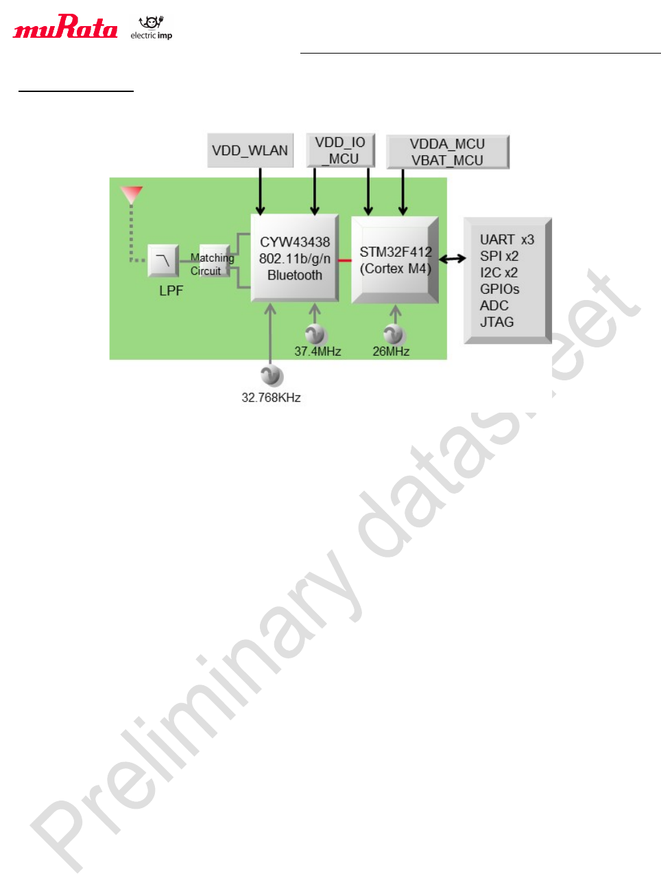
3. Block Diagram
Note: 32.768KHz outside of module
Preliminary Specification Number : SP-ZZ1MD-J
6 / 34
Preliminary
< Specification may be changed by Murata without notice >
Murata Manufacturing Co., Ltd.
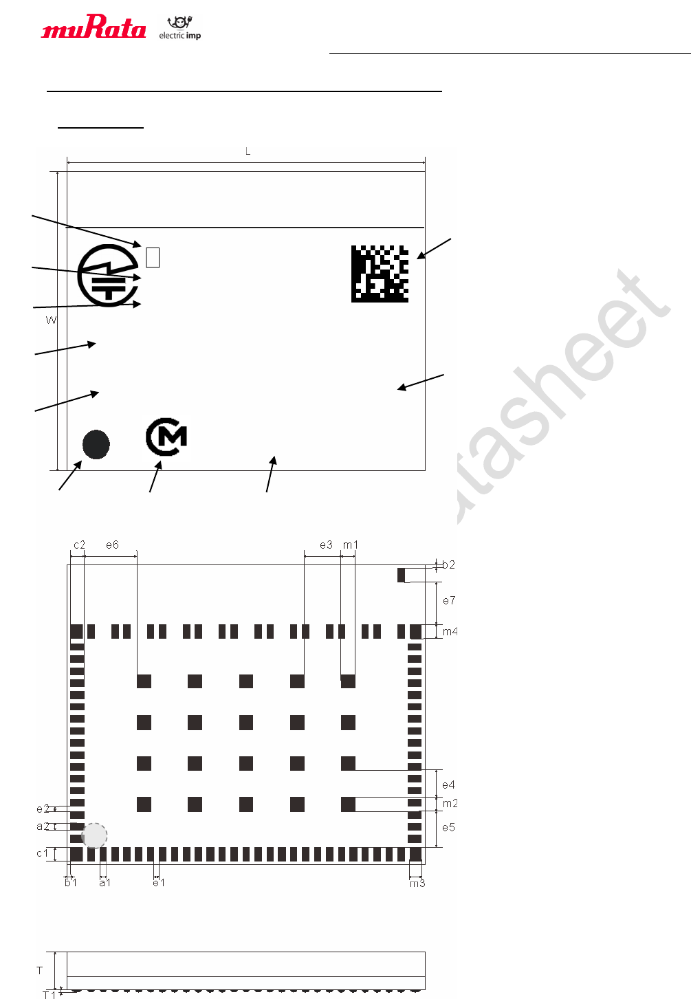
4. Dimensions, Marking and Terminal Configurations
4.1. Dimensions
< Side View
>
< Top View >
< Top View >
XXXXXXXXX
(F)
imp004m
(E)
(B)
(G)
electricimp
(C)
(A)
Model:Type1MD
R 001-P01018
FCC:VPYLB1MDIMP004
IC :772C-LB1MDIMP004
(H)
(J)
(I)
(D)
Preliminary Specification Number : SP-ZZ1MD-J
7 / 34
Preliminary
< Specification may be changed by Murata without notice >
Murata Manufacturing Co., Ltd.
Mark
Dimensions
Mark
Dimensions
Mark
Dimensions
L
21.0 +/- 0.2
W
17.5 +/- 0.2
T
2.3 max.
a1
0.4 +/- 0.1
a2
0.4 +/- 0.1
b1
0.2 +/- 0.2
b2
0.2 +/- 0.2
c1
0.8 +/- 0.1
c2
0.8 +/- 0.1
e1
0.3 +/- 0.1
e2
0.3 +/- 0.1
e3
2.2 +/- 0.1
e4
1.6 +/- 0.1
e5
2.1 +/- 0.1
e6
3.1 +/- 0.1
e7
2.5 +/- 0.1
m1
0.8 +/- 0.1
m2
0.8 +/- 0.1
m3
0.7 +/- 0.1
m4
0.8 +/- 0.1
(unit : mm)
Marking
Marking
Meaning
(A)
Pin 1 Marking
(B)
Murata Logo
(C)
Electric Imp Logo
(D)
Murata Module Type
(E)
Imp Module Type
(F)
Inspection Number
(G)
2D code
(H)
Japanese Type certification No.
(I)
FCC certification ID
(J)
IC certification No.
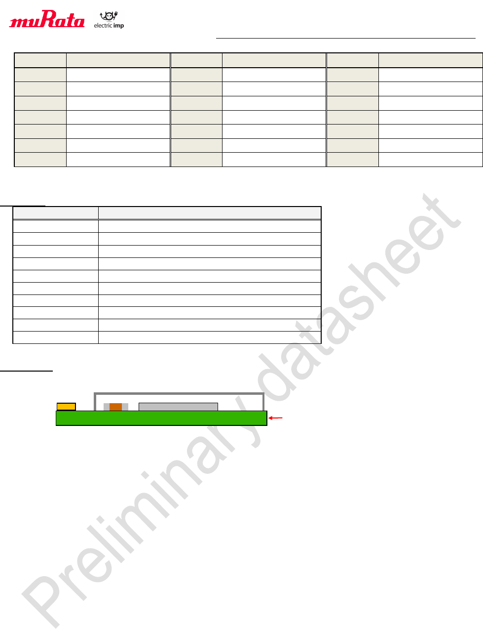
Structure
PWB
Metal!Case
PCB!Trace
Antenna
Preliminary Specification Number : SP-ZZ1MD-J
8 / 34
Preliminary
< Specification may be changed by Murata without notice >
Murata Manufacturing Co., Ltd.
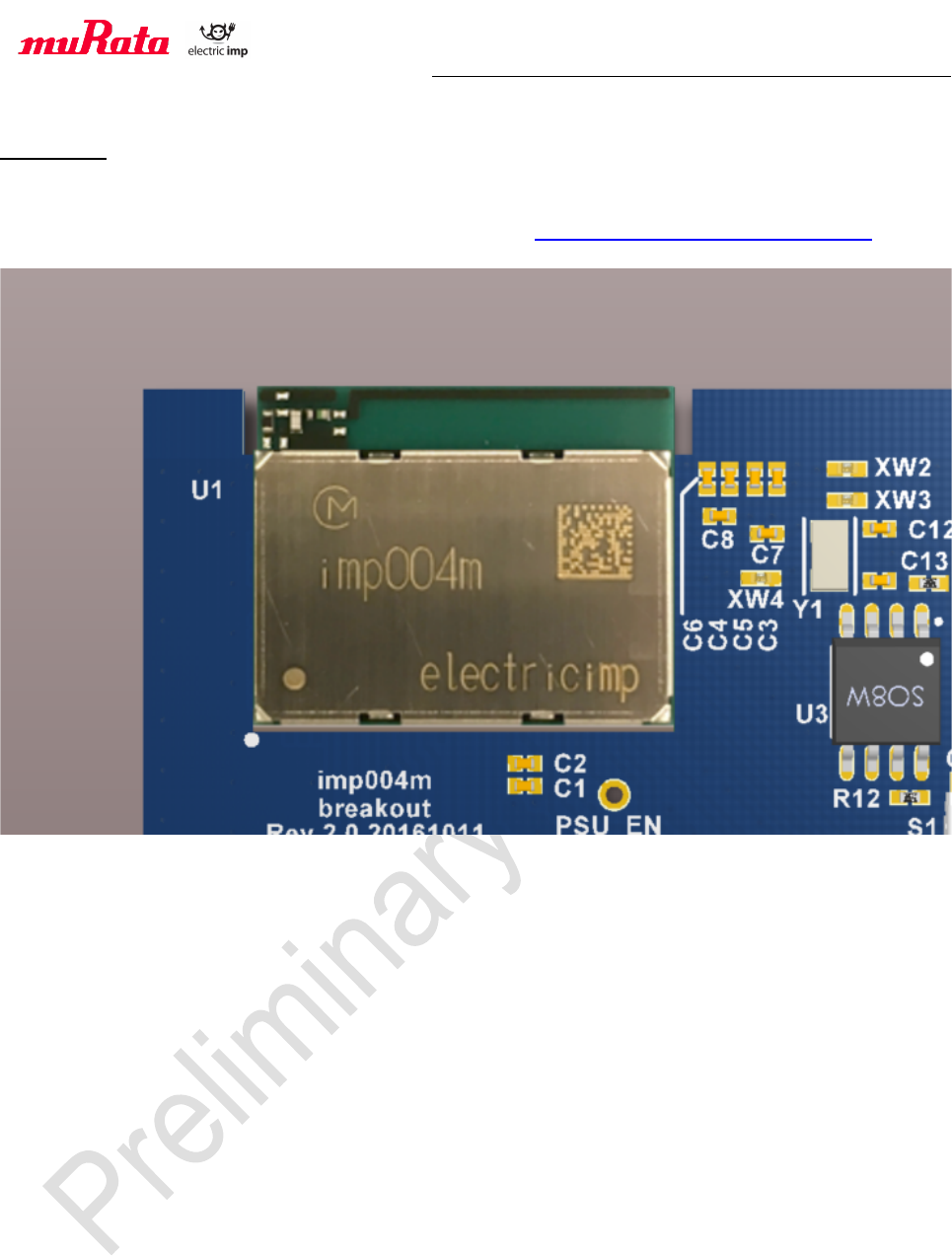
Mounting
The module is designed to be mounted on the edge of the board, with the antenna section
hanging off in free space. The antenna is tuned for free space operation. Please see the
design guide on Electric Imp dev center website at http://www.electricimp.com/docs for
more information.
Preliminary Specification Number : SP-ZZ1MD-J
9 / 34
Preliminary
< Specification may be changed by Murata without notice >
Murata Manufacturing Co., Ltd.
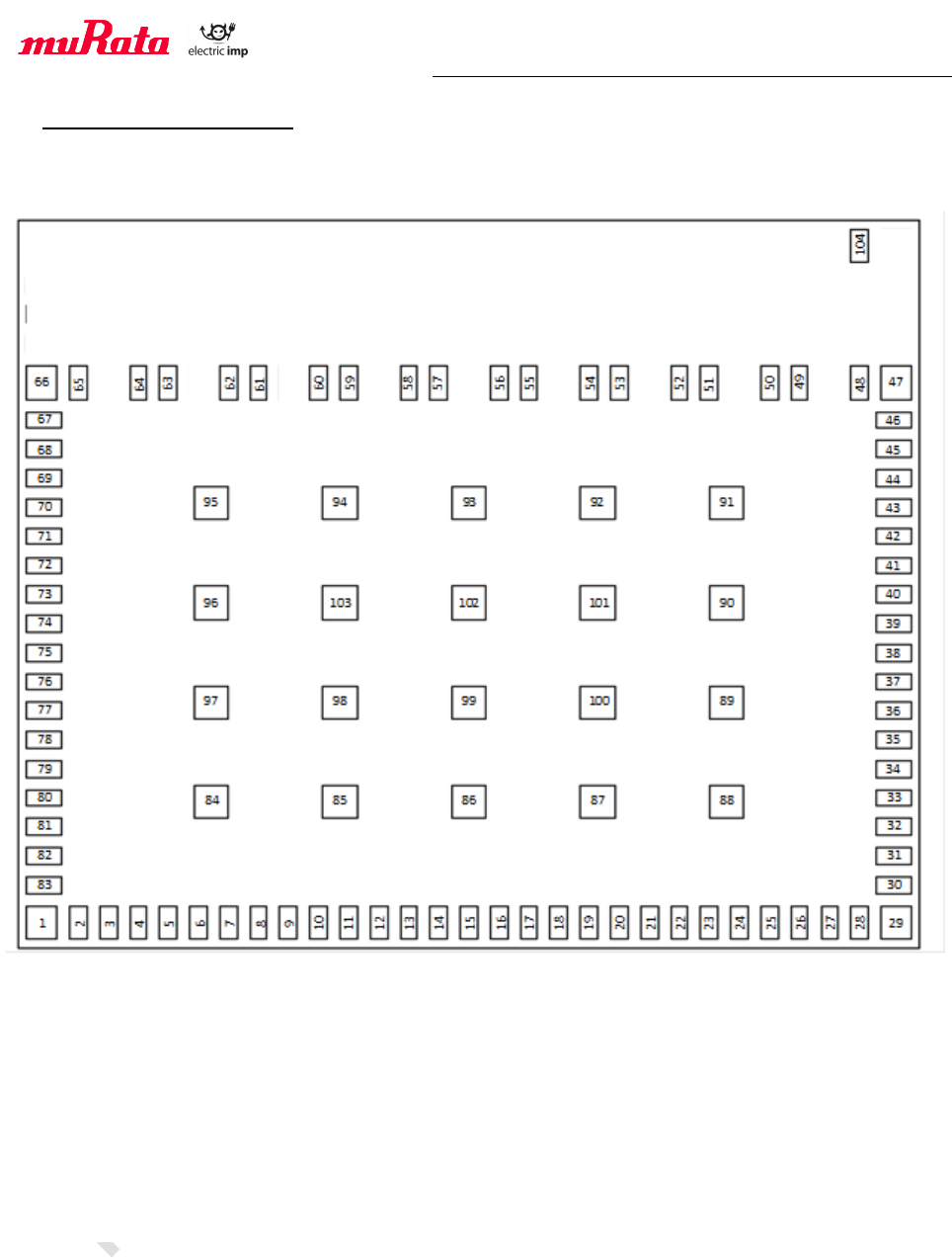
4.2. Terminal Configurations
Top view (through package)

Preliminary Specification Number : SP-ZZ1MD-J
10 / 34
Preliminary
< Specification may be changed by Murata without notice >
Murata Manufacturing Co., Ltd.
No.
Name
Type
Description
1
GND
GND
2
CLK_REQ
O
Reference clock request. As the clock is internal, this pin
does not need to be connected
3
BT_REG_ON
I
Enable Bluetooth power. Leave NC if Bluetooth is not
used (active high)
4
NC
-
No Connect
5
pinM
I/O
GPIO, i2cNM SDA, PWM
6
pinN
I/O
GPIO, i2cNM SCL, PWM
7
pinP
I/O
GPIO, i2cQP SDA, PWM, IRQ
8
pinW
I/O
GPIO, uartBCAW CTS, ADC, IRQ & wake from
deep sleep (active high)
9
GND
GND
10
pinA
I/O
GPIO, uartBCAW RTS, spiAHSR MOSI, ADC,
PWM
11
pinB
I/O
GPIO, uartBCAW TX, ADC, PWM, IRQ
12
pinC
I/O
GPIO, uartBCAW RX, ADC, IRQ
13
LPO_IN
I
Sleep Clock (for both WiFi & Bluetooth). If low
power WiFi operation – or Bluetooth operation – is
required, this pin should be connected to pinE.
Otherwise, ground this pin.
14
pinD
I/O
GPIO, ADC, PWM, IRQ
15
pinE
I/O
GPIO, IRQ
16
pinK
I/O
GPIO, spiGJKL SCLK, ADC, PWM
17
pinL
I/O
GPIO, spiGJKL NSS, ADC, IRQ
18
GND
GND
19
VDD_IO_MCU
PWR
MCU/WLAN VIO
20
GND
GND
21
pinQ
I/O
GPIO, uartQ TX, i2cQP SCL, IRQ
22
pinR
I/O
GPIO, spiAHSR NSS, IRQ
23
pinS
I/O
GPIO, spiAHSR SCLK, IRQ
24
PSU_ENABLE
O
Active high when WiFi needs 2.7v+
25
pinF
I/O
GPIO, uartFGJH TX
26
pinG
I/O
GPIO, uartFGJH RX, spiGJKL MOSI
27
pinH
I/O
GPIO, uartFGJH CTS, uartHJ TX, spiAHSR MISO,
IRQ
28
pinJ
I/O
GPIO, uartFGJH RTS, uartHJ RX, spiGJKL MISO,
pulse counter
29
GND
GND
30
LED_RED
O
Red LED drive
31
LED_GREEN
O
Green LED drive
32
OPTO_IN
I
Phototransistor input
33
OPTO_BIAS
O
Phototransistor supply
34
FLASH_MOSI
O
SPI flash connection
35
FLASH_SCLK
O
SPI flash connection
36
FLASH_CS_L
O
SPI flash connection

Preliminary Specification Number : SP-ZZ1MD-J
11 / 34
Preliminary
< Specification may be changed by Murata without notice >
Murata Manufacturing Co., Ltd.
37
FLASH_MISO
I
SPI flash connection
38
NC
-
39
RESET_L
I
MCU reset, internally pulled up
40
VSSA/VREF-
GND
Must be connected to GND
41
OSC32_OUT
O
32kHz xtal connection
42
OSC32_IN
I
32kHz xtal connection (ground if no xtal fitted)
43
GND
GND
44
VBAT_MCU
PWR
MCU VBAT input
45
VDDA_MCU
PWR
MCU VDDA input
46
VDD_WLAN
PWR
WLAN VBAT input
47-70
GND
GND
71
BT_UART_TXD
O
Bluetooth UART transmit. Leave NC if not used
72
BT_UART_RTS
O
Bluetooth UART ready to send. Leave NC if not used
73
BT_UART_RXD
I
Bluetooth UART receive. Leave NC if not used
74
BT_UART_CTS
I
Bluetooth UART clear to send. Leave NC if not used
75-76
GND
GND
77
BT_HOST_WAKE
O
Signal to wake host (from Bluetooth core). Leave NC if not
used
78-81
NC
-
82
BT_DEV_WAKE
I
Signal to wake Bluetooth core (from host). Leave NC if not
used
83
NC
-
No Connect
84-103
GND
GND
104
NC
-
Note this pad should not be touching any PCB

Preliminary Specification Number : SP-ZZ1MD-J
12 / 34
Preliminary
< Specification may be changed by Murata without notice >
Murata Manufacturing Co., Ltd.
4.3. Pin Mux table
Pin
Uart
BCAW
uart
FGJH
uart
HJ
uart
Q
i2c
NM
i2c
QP
spi
AHSR
spi
GJKL
ADC
PWM
Pulse
count
State
change
pinA
RTS
MOSI
Yes
Yes
pinB
TX
Yes
Yes
Yes
pinC
RX
Yes
Yes
pinD
Yes
Yes
Yes
pinE
Yes
pinF
TX
pinG
RX
MOSI
pinH
CTS
TX
MISO
Yes
pinJ
RTS
RX
MISO
Yes
pinK
SCLK
Yes
Yes
pinL
NSS
Yes
Yes
pinM
SDA
Yes
pinN
SCL
Yes
pinP
SDA
Yes
Yes
pinQ
TX
SCL
Yes
pinR
NSS
Yes
pinS
SCLK
Yes
pinW
CTS
Yes
Yes
Preliminary Specification Number : SP-ZZ1MD-J
13 / 34
Preliminary
< Specification may be changed by Murata without notice >
Murata Manufacturing Co., Ltd.
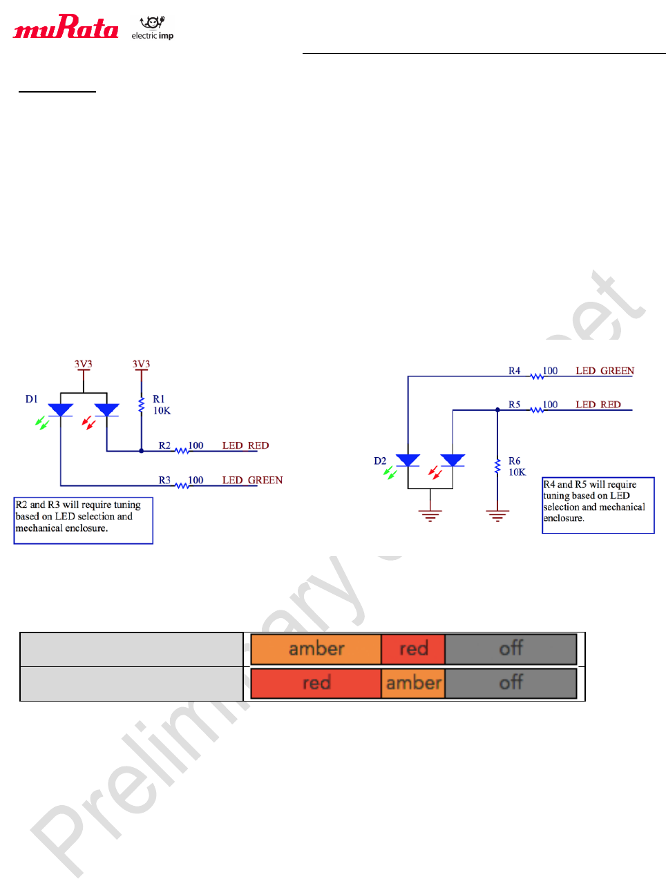
5. LED drive
The indicator LED should be bicolor, because red, green and amber (red+green) are used
to indicate status.
The LED drive pins will auto-detect common anode or common cathode parts. The
detection is done by looking to see which way up the LED_RED pin is idling at boot; to
ensure this works correctly, please place a 10k resistor in parallel with the red LED.
The current drive on these pins is 20mA maximum.
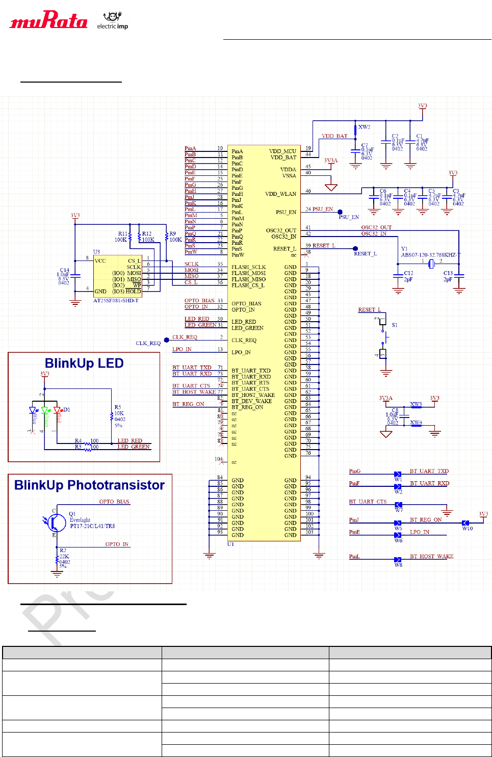
Please refer to section 15 for the recommended LEDs.
<Common anode diagram> <Common cathode diagram>
Two specific LED codes indicate errors when talking to the SPI flash:
SPI flash not found
SPI flash error
If you encounter either of these codes, then this indicates an electrical connection issue or
an incompatible flash part.
Preliminary Specification Number : SP-ZZ1MD-J
14 / 34
Preliminary
< Specification may be changed by Murata without notice >
Murata Manufacturing Co., Ltd.
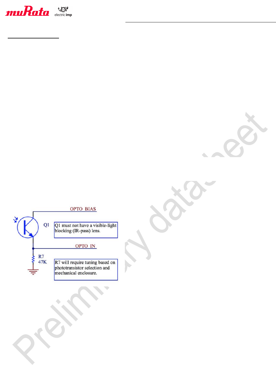
6. Phototransistor
The phototransistor is used to receive BlinkUp configuration data. The bias resistor
connected between OPTO_IN and GND may need to be adjusted to ensure adequate
sensitivity and response time - in general you need at least 500mV swing on the OPTO_IN
pin between black and white states, with the worst (dimmest) BlinkUp sender you can find.
More information and sample code to tune blinkup is available on the Electric Imp dev
center website.
End-user BlinkUp send data at between 30 and 60 bits per second, depending on the
user’s device. For factory configuration, data is typically sent at 142 bits per second using
red LED(s) in a test fixture. If your application does not require optical configuration, config
can be sent electrically at 142 bits per second from another micro using the OPTO_IN pin.
Please contact us for more details.
It is also recommended to place 0402, 13pF capacitor footprints (Murata
GRM1555C1H130JA01) close to the imp004m between OPTO_BIAS and GND, and
OPTO_IN and GND. If issues are seen with RF coupling onto the blinkup circuit, then these
components will address the issue by presenting a low impedance in the 2.4GHz band.
Please refer to paragraph 15 for the recommended phototransistors.
Preliminary Specification Number : SP-ZZ1MD-J
15 / 34
Preliminary
< Specification may be changed by Murata without notice >
Murata Manufacturing Co., Ltd.
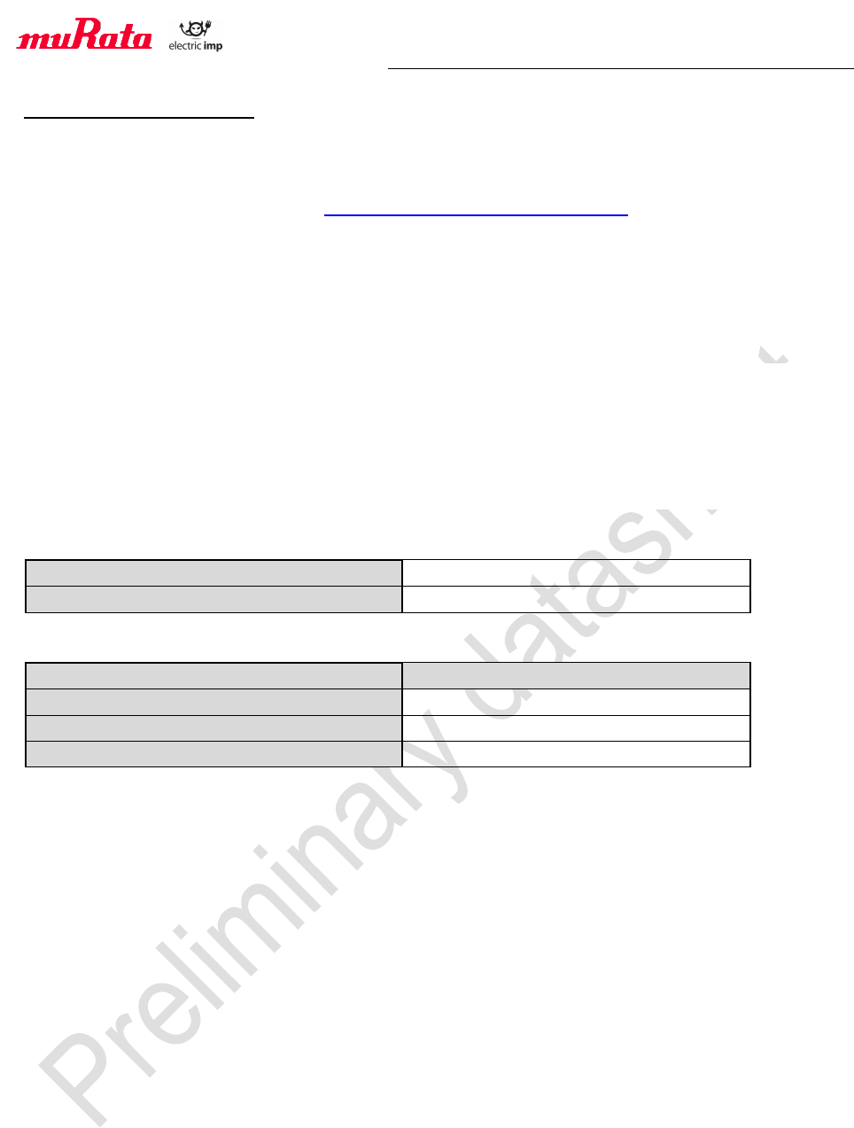
7. SPI flash requirements
An external SPI Flash part is required for operation, which must be pre-loaded with the
correct WiFi firmware image before assembly. The required image is available from the
Electric Imp dev center website at http://www.electricimp.com/docs
The minimum size of the SPI Flash is 8Mbit (1MB), and the maximum size is 128Mbit
(16MB). The area below address 0xC2000 (776kB) is the pre-programmed area. The
remainder of the flash device is made available to user code programmatically, and may
optionally be pre-programmed for user applications before assembly.
The imp004m’s SPI flash chip must support both 4KB erases (Command 0x20) and 64KB
erases (command 0xD8) and Page Program (command 0x02). You must also ensure that
the SPI flash you use is able to run down to the minimum operational voltage of your
product to ensure that the SPI flash is operational at all times that the imp is operational.
This is critical during upgrades in low battery states. If you are running from a single
LiMnO2 cell (eg. CR123), you should use a wide voltage range SPI flash that is operational
from 1.7-3.6V such as the Macronix MX25R8035FM2IH0.
Minimum Size
8 Mbit (1024 kByte)
Reserved for OS (do not pre-program)
0x000000 to 0xC2000 (776 kByte)
Summary of required SPI flash commands
Required Command
Command in Hex
4KB Sector Erase
0x20
64KB Block Erase
0xD8
Page Program
0x02

Preliminary Specification Number : SP-ZZ1MD-J
16 / 34
Preliminary
< Specification may be changed by Murata without notice >
Murata Manufacturing Co., Ltd.
8. Required wiring for Bluetooth operation
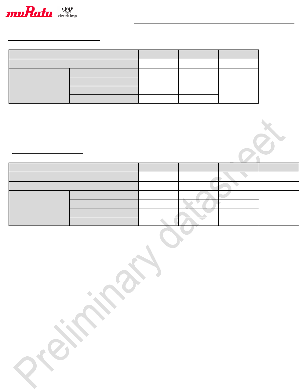
If Bluetooth is not used in the application, leave all Bluetooth pins (3, 71-74, 77, 82)
unconnected.
To use Bluetooth in an application, you must connect the MCU pins to the Bluetooth device:
• BT_UART_TXD should be connected to an MCU UART RX pin (pinC, pinG or pinJ)
• BT_UART_RXD should be connected to the same UART’s TX pin (pinB, pinF or
pinH)
• pinE MUST be connected to the LPO in pin, to supply a 32kHz clock to the Bluetooth
radio
• BT_REG_ON should be connected to any free MCU pin, to control Bluetooth power
• BT_UART_CTS should be grounded (The imp Bluetooth stack uses 2 wire UART)
Aside from pinE, which cannot be reassigned, choice of UART and control pin for
BT_REG_ON is determined by the application – this allows flexibility in complex IO
configurations.
Please refer to the Electric Imp dev center for more information on how to configure the
Bluetooth stack, which is present from impOS release 40.
Note that though use of Bluetooth is free for developers, commercial use incurs an
additional licensing fee for the stack. Please contact sales@electricimp.com for more
details.
Preliminary Specification Number : SP-ZZ1MD-J
17 / 34
Preliminary
< Specification may be changed by Murata without notice >
Murata Manufacturing Co., Ltd.
9. Absolute Maximum Rating
min.
max.
unit
Storage Temperature
-40
85
deg.C
Supply Voltage
VBAT_MCU
-0.3
4
V
VDDA_MCU
-0.3
4
VDD_WLAN
-0.5
6
VDD_IO_MCU
-0.3
3.63
Stresses in excess of the absolute ratings may cause permanent damage. Functional operation is not implied under
these conditions. Exposure to absolute ratings for extended periods of time may adversely affect reliability. No
damage assuming only one parameter is set at limit at a time with all other parameters is set within operating
condition.
10. Operating Condition
min.
typ.
max.
unit
Operating Temperature Range
-30
25
70
deg.C
Specification Temperature Range
-20
25
55
deg.C
Supply Voltage
VBAT_MCU
1.65
3.3
3.6
V
VDDA_MCU
1.8
3.3
3.6
VDD_WLAN
3.0
3.3
3.6
VDD_IO_MCU
1.8
3.3
3.6
Notes :
n All RF characteristics in this datasheet are defined by Specification Temperature
Range. Specifications require derating at extreme temperatures.
n VDDA_MCU and VDD_IO_MCU must be the same potential.

Preliminary Specification Number : SP-ZZ1MD-J
18 / 34
Preliminary
< Specification may be changed by Murata without notice >
Murata Manufacturing Co., Ltd.
11. External 32.768 kHz Crystal
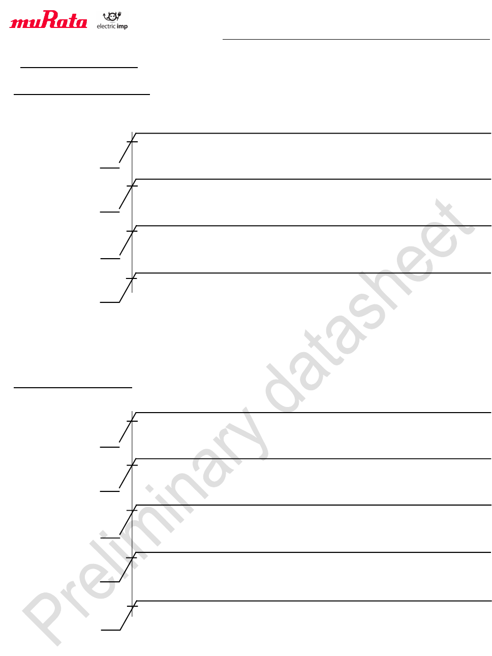
If the application requires the imp004m to enter deep sleep mode, a 32kHz crystal should
be attached to the OSC32_IN and OSC32_OUT pins. Please refer to the STM32F412
datasheet and application note AN2867 by STMicroelectronics NV for detailed crystal
requirements.
If deep sleep mode is not required, OSC32_IN should be connected to GND and
OSC32_OUT left floating. The imp004m will detect this state and disable the sleep APIs.
Preliminary Specification Number : SP-ZZ1MD-J
19 / 34
Preliminary
< Specification may be changed by Murata without notice >
Murata Manufacturing Co., Ltd.
12. Power Up Sequence
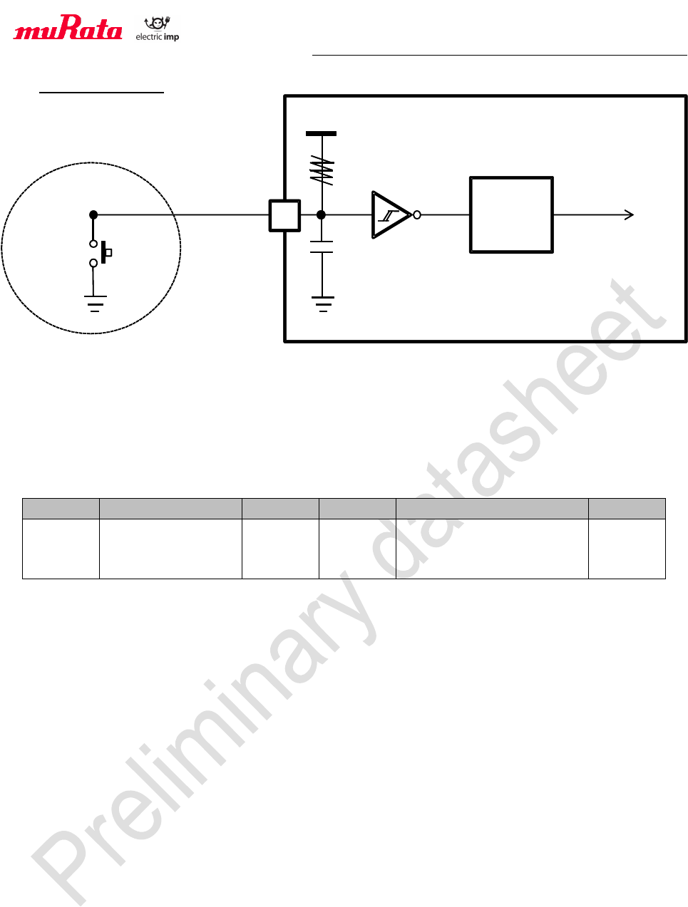
12.1. Without RESET_L control
Following timing diagram explain module power up sequence.
*Power down sequence is opposite sequence of power up.
12.2. With RESET_L control
*Power down sequence is opposite sequence of power up.
*RESET_L pin must be controlled by Open Drain.
VBAT_MCU
Ramp time 90% > 40µs
VDD_WLAN
VDDA_MCU
Timing same as VBAT_MCU
VDD_IO_MCU
VBAT_MCU
Ramp time 90% > 40µs
VDD_WLAN
VDDA_MCU
Timing same as VBAT_MCU
VDD_IO_MCU
RESET_L
Timing of deassertioRESET_L signal same as VDD_IO
Timing same as VBAT_MCU
Timing same as VBAT_MCU
Timing same as VBAT_MCU
Timing same as VBAT_MCU
Preliminary Specification Number : SP-ZZ1MD-J
20 / 34
Preliminary
< Specification may be changed by Murata without notice >
Murata Manufacturing Co., Ltd.
12.3. RESET_L Circuit
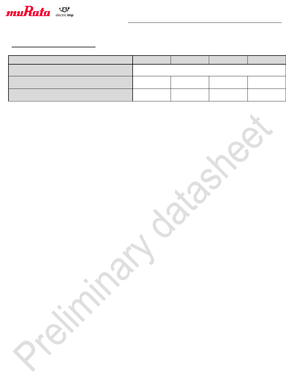
(1) The reset network protects the device against parasitic resets.
(2) The use must ensure that the level on the RESET_L pin can go below the VIL(NRST) max level
specified in below table. Otherwise the reset is not taken into account by the device.
(3) RESET_L pin must be controlled by Open Drain. High signal must not input to this pin.
Symbol
Parameter
Min
Typ
Max
Unit
VIL
RESET_L I/O
input low level
voltage
-
-
0.1xVDD_IO_MCU+0.1
V
Filter
Internal
Reset
V
DD_IO_MCU (3)
40kΩ
RESET_L
(2
)
External
Reset circuit
(1)
Murata
Module
0.1uF
Preliminary Specification Number : SP-ZZ1MD-J
21 / 34
Preliminary
< Specification may be changed by Murata without notice >
Murata Manufacturing Co., Ltd.
13. Electrical Characteristics
- DC Characteristics -
min.
typ.
max.
unit
1. DC current
1) Tx mode1)
300
370
mA
2) Rx mode
45
100
mA
1) Conditions: 25deg.C, VDD_WLAN=3.3V, VDD_IO_MCU=3.3V
(1Mbps mode unless otherwise specified.)
Note: The above mentioned values have been obtained according to our own measuring
methods and may very depend on the circuit, in which the component is actually
incorporated. Therefore, you are kindly requested to test the performance of the
component actually in your set.
Preliminary Specification Number : SP-ZZ1MD-J
22 / 34
Preliminary
< Specification may be changed by Murata without notice >
Murata Manufacturing Co., Ltd.
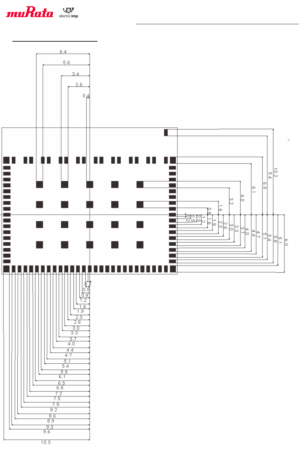
14. Land pattern (Top View)
Unit : mm
Preliminary Specification Number : SP-ZZ1MD-J
23 / 34
Preliminary
< Specification may be changed by Murata without notice >
Murata Manufacturing Co., Ltd.
15. Reference Circuit
16. Recommended Components
16.1. Bi-color LED
Manufacturer
Manufacturer’s part number
Surface mount
top-view
SunLED
XZMDKVG59W-1
Liteon
LTST-C195KGJRKT
side-view
SunLED
XZMDKVG88W
Bivar
SM1204BC
Through-hole
3mm
SunLED
XLMDKVG34M
Liteon
LTL1BEKVJNN

Preliminary Specification Number : SP-ZZ1MD-J
24 / 34
Preliminary
< Specification may be changed by Murata without notice >
Murata Manufacturing Co., Ltd.
16.2. Phototransistor
Manufacturer
Manufacturer’s part number
Surface mount
top-view
Everlight
PT17-21C/L41/TR8
Fairchild
KDT00030TR
side-view
SunLED
XZRNI56W-1
Everlight
PT12-21C/TR8
Through-hole
3mm
SunLED
XRNI30W-1
LiteOn
LTR-4206
16.3. SPI Flash
Size
Manufacturer
Manufacturer’s part number
8 Mbit
Adesto Technologies
Macronix International
AT25SF081
MX25R8035F(1)
16 Mbit
Adesto Technologies
Cypress Semiconductor Corp
AT25SF161
S25FL116K(2)
32 Mbit
Adesto Technologies
Cypress Semiconductor Corp
AT25SF321
S25FL132K(2)
64 Mbit
Cypress Semiconductor Corp
Cypress Semiconductor Corp
S25FL064L
S25FL164K(2)
(1) This device offers a wide operating voltage range
(2) This part is EOL, though inventory may still be available through distributors
Preliminary Specification Number : SP-ZZ1MD-J
25 / 34
Preliminary
< Specification may be changed by Murata without notice >
Murata Manufacturing Co., Ltd.
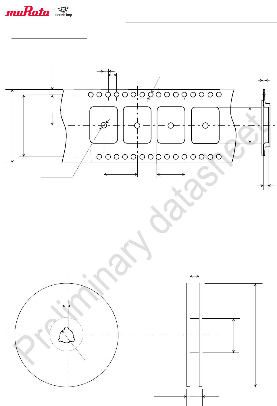
17. Tape and Reel Packing
(1) Dimensions of Tape (Plastic tape)
*1 Cumulative tolerance of max. ± 0.3 every 10 pitches
*2 Reference value
(Unit :
mm)
(2) Dimensions of Reel
(Unit: mm)
2.0±
0.15
0.3±
0.05
24.0±
0.1
1.5+0.1/-0.0
2.0+0.1/-0.0
4
.0±
0.1*1
22.00±0.10*2
.
18.00±
0.10
2.55±0.1
44.0±0.3
40.4±0.1
20.2±0.1
1.75±0.1
(f 100)
f 21±0.8
2.0±0.5
45.5
(f 330)
50.5max
Preliminary Specification Number : SP-ZZ1MD-J
26 / 34
Preliminary
< Specification may be changed by Murata without notice >
Murata Manufacturing Co., Ltd.
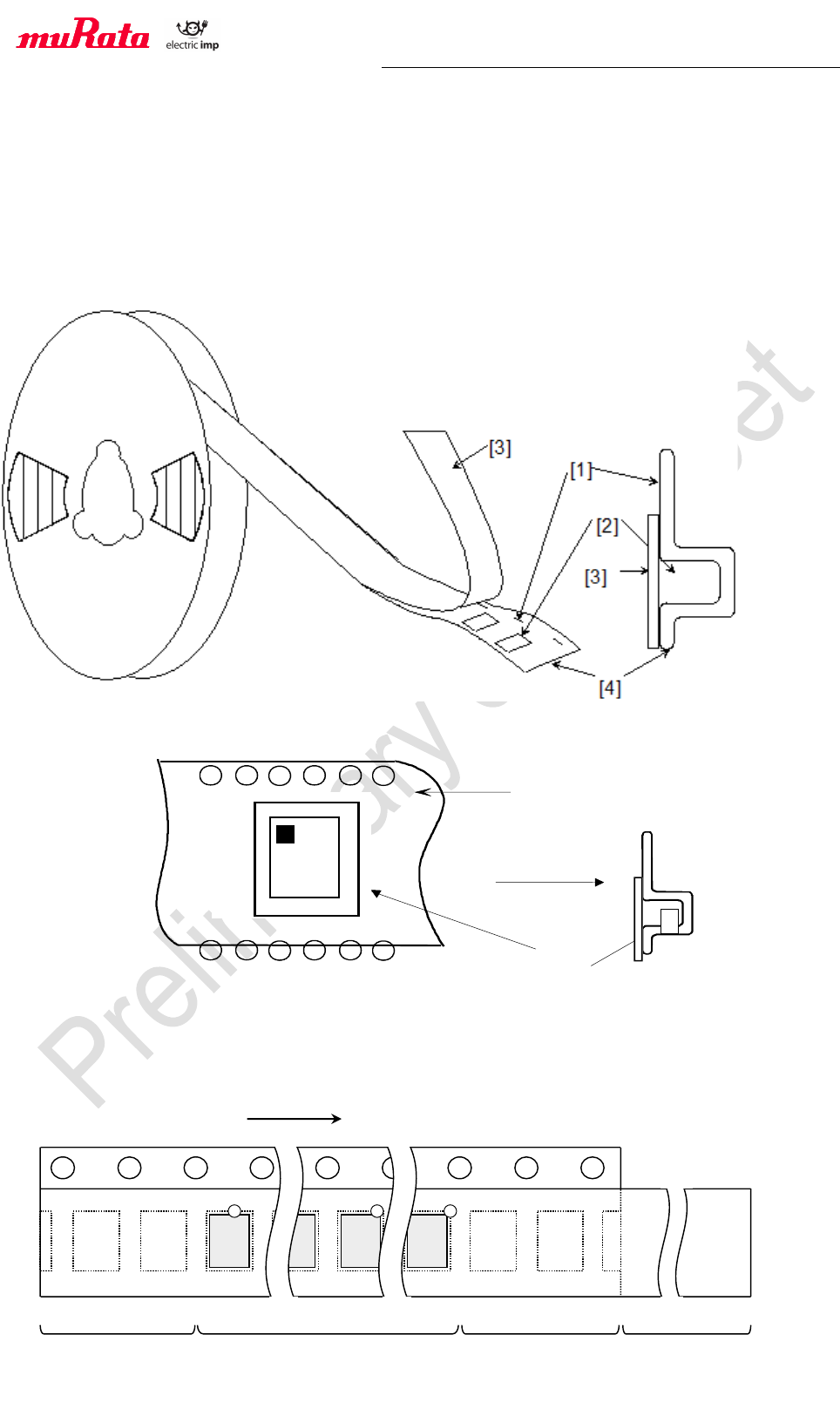
(3) Taping Diagrams
[1] Feeding Hole : As specified in (1)
[2] Hole for chip : As specified in (1)
[3] Cover tape : 62μm in thickness
[4] Base tape : As specified in (1)
(4) Leader and Tail tape
Tail tape
(No
components)
Components
No components
200mm min.
Leader tape
(Cover tape
alone)
Feeding
direction
Chi
p
Feeding
Direction
Preliminary Specification Number : SP-ZZ1MD-J
27 / 34
Preliminary
< Specification may be changed by Murata without notice >
Murata Manufacturing Co., Ltd.
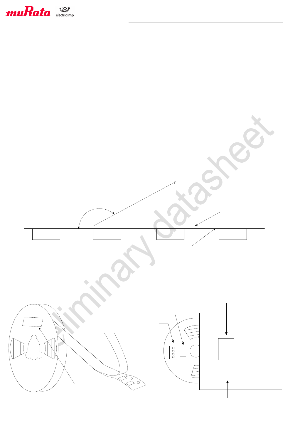
(5) The tape for chips are wound clockwise, the feeding holes to the right side as the tape
is pulled toward the user.
(6) The cover tape and the base tape are not adhered at no components area for 250mm
min.
(7) Tear off strength against pulling of cover tape : 5N min.
(8) Packaging unit: 500pcs./ reel
(9) Material: Base tape : Plastic
Reel : Plastic
Cover tape, cavity tape and reel are made the anti-static processing.
(10) Peeling of force: 1.1N max. in the direction of peeling as shown below.
(11) Packaging (Humidity proof Packing)
Tape and reel must be sealed with the anti-humidity plastic bag. The bag contains the
desiccant and the humidity indicator.
165 to 180 °
1.1 N max.
Base tape
Cover tape
湿度
インジケ-タ
乾燥剤
表示ラべル
防湿梱包袋
表示ラベル
Label
Label
Desiccant
Humidity
Indicator
Anti-humidity
Plastic Bag

Preliminary Specification Number : SP-ZZ1MD-J
28 / 34
Preliminary
< Specification may be changed by Murata without notice >
Murata Manufacturing Co., Ltd.
18. NOTICE
18.1. Storage Conditions:
Please use this product within 6month after receipt.
- The product shall be stored without opening the packing under the ambient temperature
from 5 to 35deg.C and humidity from 20 to 70%RH.
(Packing materials, in particular, may be deformed at the temperature over 40deg.C.)
- The product left more than 6months after reception, it needs to be confirmed the
solderability before used.
- The product shall be stored in non corrosive gas (Cl2, NH3, SO2, Nox, etc.).
- Any excess mechanical shock including, but not limited to, sticking the packing materials
by sharp object and dropping the product, shall not be applied in order not to damage the
packing materials.
This product is applicable to MSL3 (Based on JEDEC Standard J-STD-020)
- After the packing opened, the product shall be stored at <30deg.C / <60%RH and the
product shall be used within 168hours.
- When the color of the indicator in the packing changed, the product shall be baked before
soldering.
Baking condition: 125+5/-0deg.C, 24hours, 1time
The products shall be baked on the heat-resistant tray because the material (Base Tape,
Reel Tape and Cover Tape) are not heat-resistant.
18.2. Handling Conditions:
Be careful in handling or transporting products because excessive stress or mechanical
shock may break products.
Handle with care if products may have cracks or damages on their terminals, the
characteristics of products may change. Do not touch products with bear hands that may
result in poor solder ability and destroy by static electrical charge.
18.3. Standard PCB Design (Land Pattern and Dimensions):
All the ground terminals should be connected to the ground patterns. Furthermore, the
ground pattern should be provided between IN and OUT terminals. Please refer to the
specifications for the standard land dimensions.
The recommended land pattern and dimensions is as Murata's standard. The
characteristics of products may vary depending on the pattern drawing method, grounding
method, land dimensions, land forming method of the NC terminals and the PCB material
and thickness. Therefore, be sure to verify the characteristics in the actual set. When using
non-standard lands, contact Murata beforehand.

Preliminary Specification Number : SP-ZZ1MD-J
29 / 34
Preliminary
< Specification may be changed by Murata without notice >
Murata Manufacturing Co., Ltd.
18.4. Notice for Chip Placer:
When placing products on the PCB, products may be stressed and broken by uneven
forces from a worn-out chucking locating claw or a suction nozzle. To prevent products
from damages, be sure to follow the specifications for the maintenance of the chip placer
being used. For the positioning of products on the PCB, be aware that mechanical chucking
may damage products.
Preliminary Specification Number : SP-ZZ1MD-J
30 / 34
Preliminary
< Specification may be changed by Murata without notice >
Murata Manufacturing Co., Ltd.
18.5. Soldering Conditions:
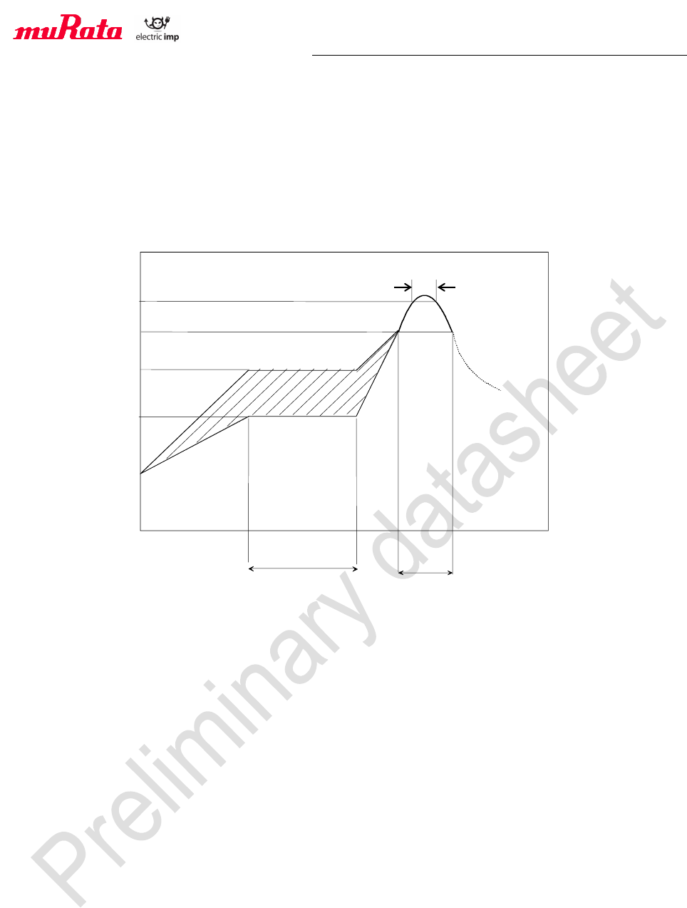
The recommendation conditions of soldering are as in the following figure.
When products are immersed in solvent after mounting, pay special attention to maintain
the temperature difference within 100 °C. Soldering must be carried out by the above
mentioned conditions to prevent products from damage. Set up the highest temperature of
reflow within 260 °C. Contact Murata before use if concerning other soldering conditions.
Reflow soldering standard conditions(Example)
Please use the reflow within 2 times.
Use rosin type flux or weakly active flux with a chlorine content of 0.2 wt % or less.
18.6. Cleaning:
Since this Product is Moisture Sensitive, any cleaning is not permitted.
18.7. Operational Environment Conditions:
Products are designed to work for electronic products under normal environmental
conditions (ambient temperature, humidity and pressure). Therefore, products have no
problems to be used under the similar conditions to the above-mentioned. However, if
products are used under the following circumstances, it may damage products and leakage
of electricity and abnormal temperature may occur.
- In an atmosphere containing corrosive gas ( Cl2, NH3, SOx, NOx etc.).
- In an atmosphere containing combustible and volatile gases.
- Dusty place.
- Direct sunlight place.
- Water splashing place.
- Humid place where water condenses.
- Freezing place.
If there are possibilities for products to be used under the preceding clause, consult with
Murata before actual use.
As it might be a cause of degradation or destruction to apply static electricity to products, do
not apply static electricity or excessive voltage while assembling and measuring.
Within 120s
Pre-heatin
g
time(s)
220
deg.C
Within 60s
Cooling down
Slowly
180 deg.C
150
deg.C
240to 250 deg.C
Within 3s

Preliminary Specification Number : SP-ZZ1MD-J
31 / 34
Preliminary
< Specification may be changed by Murata without notice >
Murata Manufacturing Co., Ltd.
18.8. Input Power Capacity:
Products shall be used in the input power capacity as specified in this specifications.
Inform Murata beforehand, in case that the components are used beyond such input power
capacity range.

Preliminary Specification Number : SP-ZZ1MD-J
32 / 34
Preliminary
< Specification may be changed by Murata without notice >
Murata Manufacturing Co., Ltd.
19. PRECONDITION TO USE OUR PRODUCTS
PLEASE READ THIS NOTICE BEFORE USING OUR PRODUCTS.
Please make sure that your product has been evaluated and confirmed from the aspect of the fitness for the specifications
of our product when our product is mounted to your product.
All the items and parameters in this product specification/datasheet/catalog have been prescribed on the premise that our
product is used for the purpose, under the condition and in the environment specified in this specification. You are
requested not to use our product deviating from the condition and the environment specified in this specification.
Please note that the only warranty that we provide regarding the products is its conformance to the specifications provided
herein. Accordingly, we shall not be responsible for any defects in products or equipment incorporating such products,
which are caused under the conditions other than those specified in this specification.
WE HEREBY DISCLAIMS ALL OTHER WARRANTIES REGARDING THE PRODUCTS, EXPRESS OR IMPLIED,
INCLUDING WITHOUT LIMITATION ANY WARRANTY OF FITNESS FOR A PARTICULAR PURPOSE, THAT THEY
ARE DEFECT-FREE, OR AGAINST INFRINGEMENT OF INTELLECTUAL PROPERTY RIGHTS.
The product shall not be used in any application listed below which requires especially high reliability for the prevention of
such defect as may directly cause damage to the third party's life, body or property. You acknowledge and agree that, if
you use our products in such applications, we will not be responsible for any failure to meet such requirements.
Furthermore, YOU AGREE TO INDEMNIFY AND DEFEND US AND OUR AFFILIATES AGAINST ALL CLAIMS,
DAMAGES, COSTS, AND EXPENSES THAT MAY BE INCURRED, INCLUDING WITHOUT LIMITATION, ATTORNEY
FEES AND COSTS, DUE TO THE USE OF OUR PRODUCTS IN SUCH APPLICATIONS.
- Aircraft equipment.- Aerospace equipment- Undersea equipment.
- Power plant control equipment- Medical equipment.
- Transportation equipment (vehicles, trains, ships, elevator, etc.).
- Traffic signal equipment. - Disaster prevention / crime prevention equipment.
-Burning / explosion control equipment
- Application of similar complexity and/ or reliability requirements to the applications listed in the above.
We expressly prohibit you from analyzing, breaking, reverse-engineering, remodeling altering, and reproducing our
product. Our product cannot be used for the product which is prohibited from being manufactured, used, and sold by the
regulations and laws in the world.
We do not warrant or represent that any license, either express or implied, is granted under any our patent right, copyright,
mask work right, or our other intellectual property right relating to any combination, machine, or process in which our
products or services are used. Information provided by us regarding third-party products or services does not constitute a
license from us to use such products or services or a warranty or endorsement thereof. Use of such information may
require a license from a third party under the patents or other intellectual property of the third party, or a license from us
under our patents or other intellectual property.
Please do not use our products, our technical information and other data provided by us for the purpose of developing of
mass-destruction weapons and the purpose of military use.
Moreover, you must comply with "foreign exchange and foreign trade law", the "U.S. export administration regulations",
etc.
Please note that we may discontinue the manufacture of our products, due to reasons such as end of supply of materials
and/or components from our suppliers.
By signing on specification sheet or approval sheet, you acknowledge that you are the legal representative for your
company and that you understand and accept the validity of the contents herein. When you are not able to return the
signed version of specification sheet or approval sheet within 30 days from receiving date of specification sheet or
approval sheet, it shall be deemed to be your consent on the content of specification sheet or approval sheet. Customer
acknowledges that engineering samples may deviate from specifications and may contain defects due to their
development status. We reject any liability or product warranty for engineering samples. In particular we disclaim liability
for damages caused by
- the use of the engineering sample other than for evaluation purposes, particularly the installation or integration in the
product to be sold by you,
-deviation or lapse in function of engineering sample,
-improper use of engineering samples.
We disclaim any liability for consequential and incidental damages.
If you can’t agree the above contents, you should inquire our sales.

Preliminary Specification Number : SP-ZZ1MD-J
33 / 34
Preliminary
< Specification may be changed by Murata without notice >
Murata Manufacturing Co., Ltd.
20. Regulatory requirements
If the OEM or system integrator incorporates the 1MD module into their final product and
wishes to reuse the 1MD module’s FCC certification, it is the OEM/system integrator’s
responsibility to ensure compliance is met on production units.
20.1. FCC Warning Notice
This device complies with Part 15 of the FCC Rules. Operation is subject to the following
two conditions: (1) this device may not cause harmful interference and (2) this device must
accept any interference received, including interference that may cause undesired
operation.
Information to Be Supplied to the End User by the OEM or Integrator
The following regulatory and safety notices must be published in documentation supplied to
the end user of the product or system incorporating an adapter in compliance with local
regulations. Host system must be labeled with “Contains FCC ID: VPYLB1MDIMP004. This
imp004m module is to be used only for mobile and fixed application. In order to re-use the
imp004m module FCC approvals, the antenna must be installed to provide a separation
distance of at least 20cm from all persons and must not be co-located with any other
antenna or transmitter. If the module is installed with a separation distance of less than
20cm from all person or is co-located or operating in conjunction with any other antenna or
transmitter then additional FCC testing and certification may be required. End-Users must
be provided with transmitter operation conditions for satisfying RF exposure compliance.
OEM integrators must ensure that the end user has no manual instructions to remove or
install the imp004m module.

Preliminary Specification Number : SP-ZZ1MD-J
34 / 34
Preliminary
< Specification may be changed by Murata without notice >
Murata Manufacturing Co., Ltd.
20.2. IC Warning Notice
This device complies with Industry Canada license-exempt RSS standard(s).
a. Common information Operation is subject to the following two conditions:
1. This device may not cause interference, and
2. This device must accept any interference, including interference that may cause
undesired operation of the device.
Cet appareil est conforme à la norme(normes) RSS exempte de licence d'Industrie Canada
a. Informations communes Son fonctionnement est soumis aux deux conditions suivantes:
1. Ce dispositive ne peut causer des interferences, et
2. Ce dispositive doit accepter toute interference, y compris les interferences qui peuvent
causer un mauvais fonctionnement du dispositive.
Information to Be Supplied to the End User by the OEM or Integrator Modular information
form OEM
Information to be Supplied to the End User by the OEM or Integrator
The following regulatory and safety notices must be published in documentation supplied to
the end user of the product or system incorporating an adapter in compliance with local
regulations. Host system must be labeled with “Contains IC: 772C-LB1MDIMP004” This
imp004m module is to be used only for mobile and fixed application. In order to re-use the
imp004m module IC approvals, the antenna(s) used in this transmitter must be installed to
provide a separation distance of at least 20cm from all persons and must not be co-located
or operating in conjunction with any other antenna or transmitter. If antenna is installed
with a separation distance of less than 20cm from all person or is co-located or operating in
conjunction with any other antenna or transmitter then additional IC testing and certification
may be required. End-Users must be provided with transmitter operation conditions for
satisfying RF exposure compliance.
OEM integrators must ensure that the end user has no manual instructions to remove or
install the imp004m module.