NEC Platforms 241 Small size 2.4GHz wireless transceiver module User Manual TY24FM E2024 DataSheet080306
NEC Engineering, Ltd. Small size 2.4GHz wireless transceiver module TY24FM E2024 DataSheet080306
User Manual
Document Number DS170-L0704-02
January 2008 (rev.1.0)
Small size 2.4GHz wireless transceiver module
「TY24FM-E2024-01」
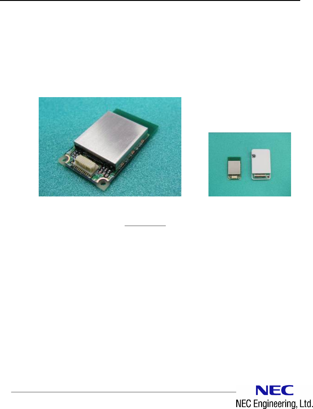
The TY24FM-E2024-01 is a 2.4GHz Low power wireless transceiver module. The
module contains all required hardware and software to evaluate and develop wireless
communication based on IEEE 802.15.4 PHY.
Product Photo
< Feature>
・ Integrated by MCU, RF circuits, antenna
・ Communicated by the functions of device detect and data transmission
・ Based on IEEE802.15.4.PHY
・ 1:N communication style
・ Controlled by UART I/F
・ Low power sleep mode
・ DC3.0V supply voltage
・ Certified CE, and FCC, Japan Radio Law
E2022 E2024
Document Number DS170-L0704-02
January 2008 (rev.1.0)
<Specification>
Product name TY24FM-E2024-01
Carrier frequency 2400MHz~2483.5MHz (16 channel)
Communication protocol Original protocol
Modulation DS-SS (Direct Sequence Spectrum Spread)
Wireless bit rate Maximum 250Kbps (Subject to the communication environment)
Transmit Power Maximum 1mW (At the feeding point of the antenna)
Transmit Distance About 40m (Reference value)
Interface ・Serial communication
Baud rate : Maximum 38.4kbps
Data length: 8bit
Parity: no parity
Stop: 1stop bit
Flow control: no flow control
Supply Voltage ・DC 3.0V (Recommended)
Current Consumption ・TX: Typ. 41mA
・RX: Typ. 43mA
・Sleep Mode : Typ. 3uA
(power-supply voltage DC 3.0V)
Operating conditions ・Operating temperature range:-15℃~+70℃
・Operating humidity range:85%RH or less (No do be dewy)
Weight About 2g
Dimensions 27.8mm×16.2mm×3.9mm (D×W×H)
Restrictions RoHS-Compliant (Pb free)
Radio Law Japan Radio Law, CE, and FCC certification

Document Number DS170-L0704-02
January 2008 (rev.1.0)
<FCC statement>
This device complies with Part 15 of the FCC Rules. Operation is subject to the following two
conditions: (1) this device may not cause harmful interference, and (2) this device must accept any
interference received, including interference that may cause undesired operation.
Modifications not expressly approved by NEC Engineering, Ltd. could void the user's authority to
operate the equipment.
This equipment has been tested and found to comply with the limits for a Class B digital device,
pursuant to Part 15 of the FCC Rules. These limits are designed to provide reasonable protection
against harmful interference in a residential installation. This equipment generates, uses and can
radiate radio frequency energy and, if not installed and used in accordance with the instructions,
may cause harmful interference to radio communications. However, there is no guarantee that
interference will not occur in a particular installation. If this equipment does cause harmful
interference to radio or television reception, which can be determined by turning the equipment off
and on, the user is encouraged to try to correct the interference by one or more of the following
measures:
-- Reorient or relocate the receiving antenna.
-- Increase the separation between the equipment and receiver.
-- Connect the equipment into an outlet on a circuit different from that to which the receiver is
connected.
-- Consult the dealer or an experienced radio/TV technician for help.
Radiofrequency radiation exposure Information:
The radiated output power of the device is far below the FCC radio frequency exposure limits.
Nevertheless, the device shall be used in such a manner that the potential for human contact during
normal operation is minimized.
Document Number DS170-L0704-02
January 2008 (rev.1.0)
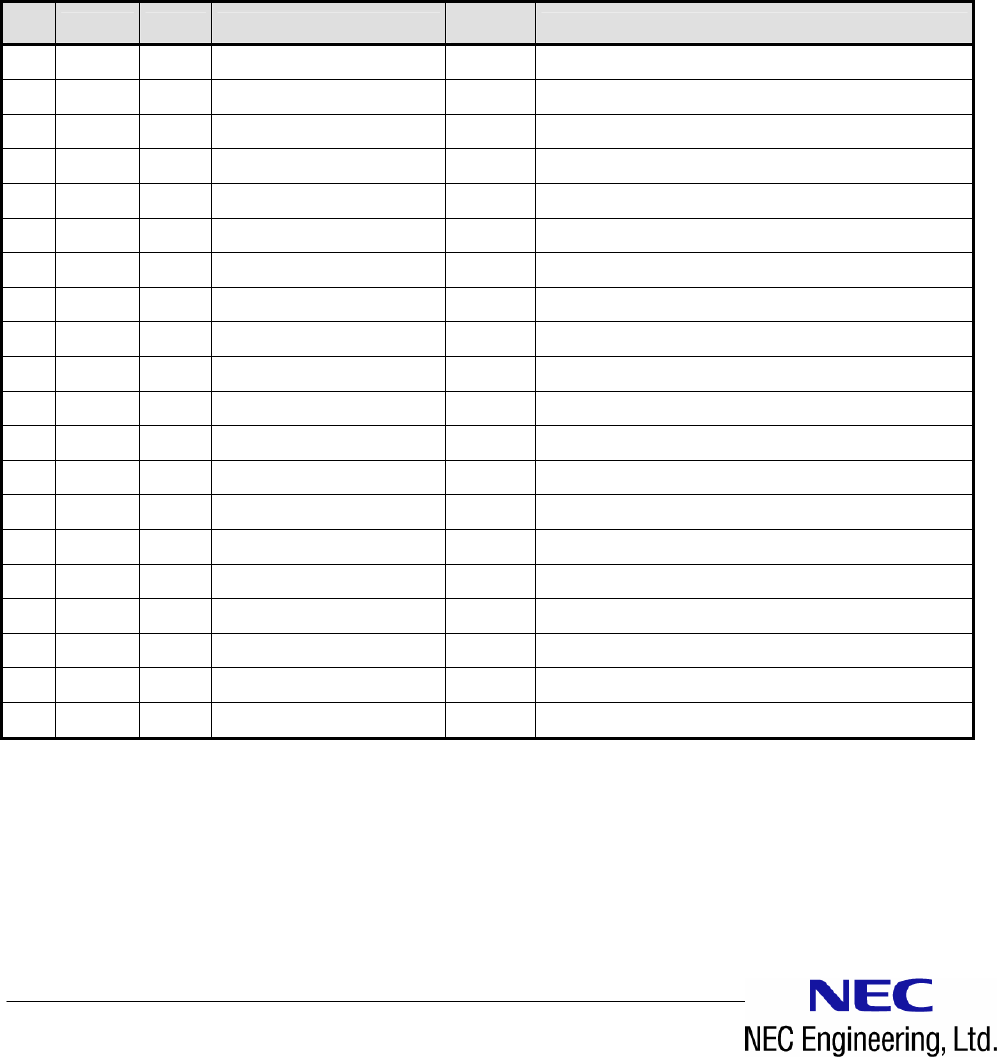
<output I/F connector>
connector type : Stacking connector 20pin 0.5mm pitch
product name : JST 20R-JMCS-G-TF(NSA) Receptacle
Signal level :CMOS
Customer : Recommended connector
JST 20P3.0-JMCS-G-TF(N) Plug
Stacking height 3mm
・Module pin definitions
Pin
No. Pin name Type Definition State of
reset Detail
1 VCC power Power - DC3.0V(Recommend power supply voltage)
2 GND GND GND -
3 TxD OUT UART data transmit HiZ
4 RxD IN UART data receive HiZ Internal Pullup
5 WAKEUP IN WAKEUP input - Sleep mode enable = High /disable = Low input
6 RESET IN RESET input - RESET Low input
7 Reserve - Reserve - n.c
8 Reserve - Reserve - n.c
9 Reserve - Reserve - n.c
10 Reserve - Reserve - n.c
11 VCC power power - DC3.0V(Recommend power supply voltage)
12 GND GND GND -
13 GND GND GND -
14 Reserve - Reserve - n.c
15 Reserve - Reserve - n.c
16 Reserve - Reserve - n.c
17 Reserve - Reserve - n.c
18 Reserve - Reserve - n.c
19 MODE OUT Mode output - Normal mode = Low / sleep mode =High output
20 GND GND GND -
Document Number DS170-L0704-02
January 2008 (rev.1.0)
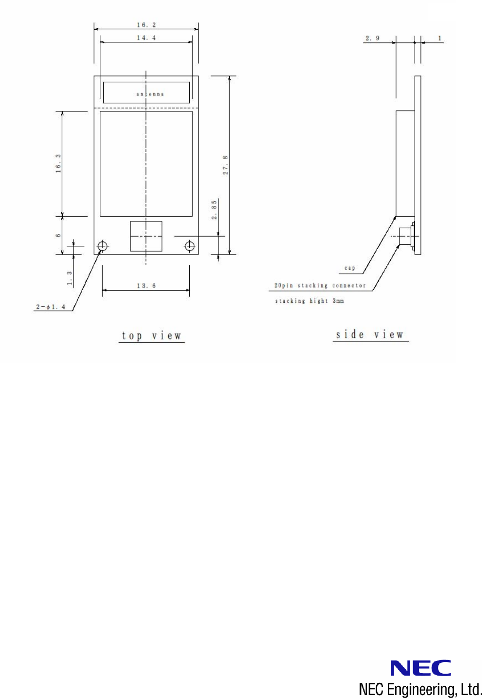
<Dimensions>
unit:mm
Document Number DS170-L0704-02
January 2008 (rev.1.0)
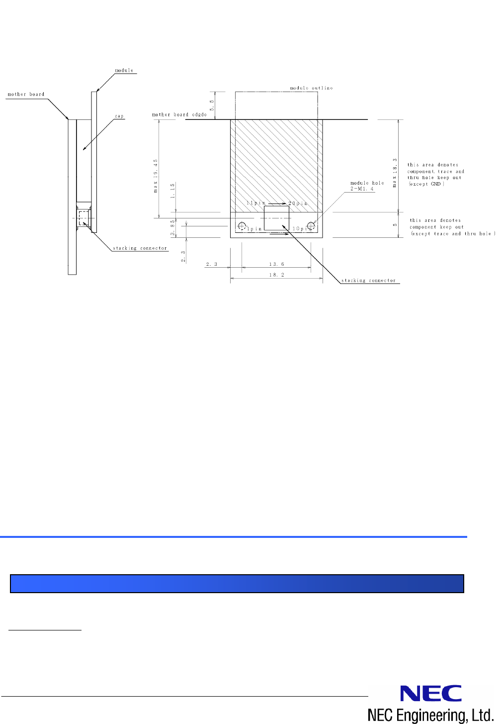
<Installation>
NEC Engineering,Ltd.
General inquiries
Sales&Marketing Division
4-10-27 Higashishinagawa Shinagawa-ku Tokyo 140-0002 Japan
TEL:
+81 3 6713 1230 URL http://www.nec-eng.com/
Contact