NEXCOM VTC6110ATT4 VTC6110-ATT4 User Manual
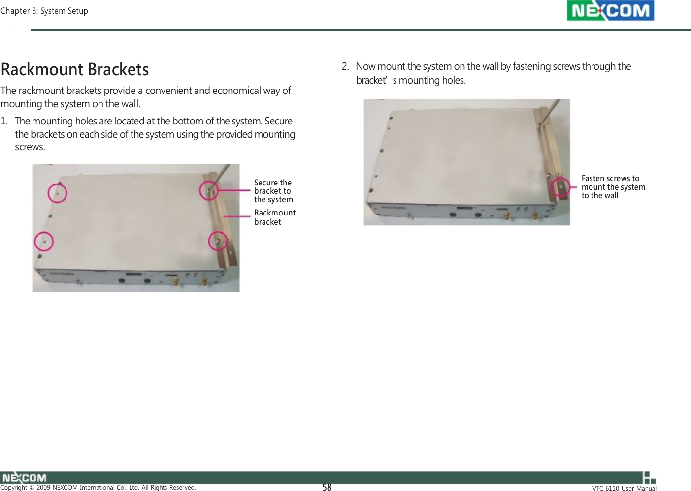
NEXCOM international Co.,LTD VTC6110-ATT4
UserManual.wiki
>
NEXCOM
>
VTC6110ATT4 User Manual
>
user manual
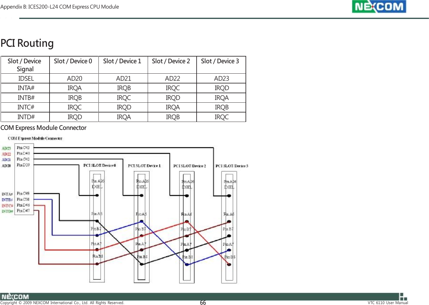
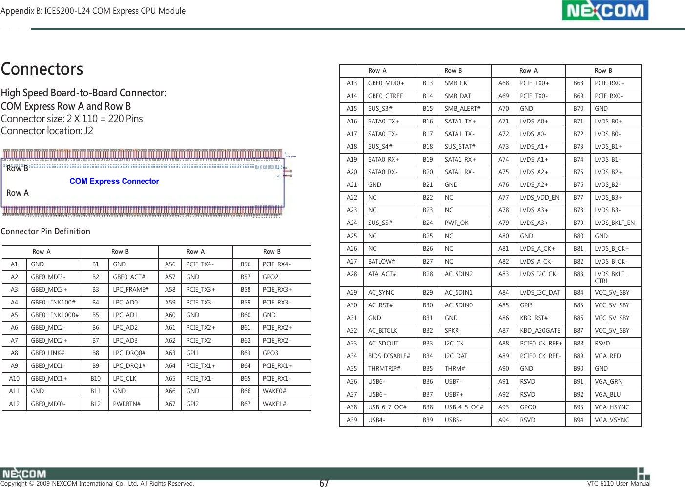
Contents
1.
user manual
2.
User manual
user manual
Navigation menu
Upload a User Manual
Namespaces
Wiki Guide
HTML
PDF
Info
Views
User Manual
Discussion / Help
Navigation