Contents
- 1. user manual
- 2. User manual
user manual

Published January 2010 www.nexcom.com
NEXCOM
International
Co.,
Ltd.
Mobile
Computing
Solutions
Vehicle
Telematics
Computer
VTC
6110ATT4
User Manual
NEXCOM
International
Co.,
Ltd.

Contents
C
ONTENTS
Preface
Copyright
.............................................................................................
iv
Disclaimer
.............................................................................................
iv
Acknowledgements
..............................................................................
iv
Regulatory
Compliance
Statements
.......................................................
iv
Declaration
of
Conformity.....................................................................
iv
RoHS
Compliance
...................................................................................
v
Warranty
and
RMA
................................................................................
vi
Safety
Information
...............................................................................
vii
Installation
Recommendations...............................................................
vii
Safety
Precautions................................................................................
viii
Technical
Support
and
Assistance
...........................................................
ix
Conventions
Used
in
this
Manual
...........................................................
ix
Global
Service
Contact
Information.........................................................
x
Package
Contents
.................................................................................
xii
Ordering
Information
...........................................................................
xiv
Chapter
1:
Product
Introduction
Overview
...............................................................................................
1
Key
Features
..........................................................................................
2
Hardware
Specifications.........................................................................
2
COM
Express
CPU
Module
and
Carrier
Board.........................................
5
Physical
Features
....................................................................................
6
Front
Panel
..........................................................................................
6
Rear
Panel
...........................................................................................
8
Mechanical
Dimensions........................................................................
12
Chapter
2:
Jumpers
And
Connectors
Before
You
Begin
.................................................................................
13
Precautions
..........................................................................................
13
Jumper
................................................................................................
14
Locations
of
the
Jumpers
and
Connectors
............................................
15
VTCB6110.........................................................................................
15
Jumper
Settings
...................................................................................
16
SW5:
Input
Voltage
Selection.............................................................
16
SW6:
COM
Port
Mode
Selection........................................................
16
CF
(IDE0)
Primary
Master/Slave
Select
(JP4).........................................
16
LVDS
Power
Input
Voltage
Select
(JP9)
...............................................
16
CMOS
Input
Voltage
Select
(J6)..........................................................
16
BIOS
Function
Select
(J1)....................................................................
16
DC
Input
Voltage
Select
(JP1).............................................................
16
Temp
Sensor
(JP8)..............................................................................
17
Auto
Power
Select
(JP2)
.....................................................................
17
PCI-104
VI/O
Select
Voltage
(J13).......................................................
17
MCU
Download
(JP6)
........................................................................
17
GAL
Download
(JP5)..........................................................................
17
MCU
COM
Port
(JP3).........................................................................
17
Connectors
..........................................................................................
18
COM
Express
Row
A
and
Row
B
........................................................
18
COM
Express
Row
C
and
Row
D........................................................
20
CompactFlash
Connector...................................................................
22
GPIO
Connector
................................................................................
23
RS232
Connector:
COM1,
COM2......................................................
23
Copyright
©
2009
NEXCOM
International
Co.,
Ltd.
All
Rights
Reserved.
ii
VTC
6110
User
Manual

Contents
RS232/485
Connector:
COM3
...........................................................
24
GAL
Programmer
PIN
Header.............................................................
24
MCU
Programmer
Pin
Header............................................................
25
VGA
Connector.................................................................................
25
LVDS
Connector
+
USB0
....................................................................
26
LAN
Connector..................................................................................
27
USB
Connector
USB
1........................................................................
27
USB
Connector
USB
2........................................................................
28
LVDS
Power
Connector......................................................................
28
External
12V
&
5V
Power
and
SMBUS
Connector
..............................
29
Mic-in................................................................................................
29
Line-out.............................................................................................
30
PCI-104
VI/O
Voltage
Setting
.............................................................
30
PCI-104
Connector............................................................................
31
Power
Button
....................................................................................
31
Reset
Button......................................................................................
31
MCU
COM
Port.................................................................................
32
ACC_ON
LED
....................................................................................
32
Temp
Sensor......................................................................................
33
DC
Power
Input
Connector................................................................
33
Power
On
and
IDE
Active
LED
............................................................
34
GPIO
and
UMTS
LEDs
........................................................................
34
Serial
ATA
..........................................................................................
35
Serial
ATA
Power
Input
......................................................................
35
Mini-PCIe
Socket
(for
3.5G
module)
PCIe
Interface.............................
36
Mini-PCIe
Socket
(for
WLAN
module)
USB
+
PCIe
Interface
................
36
SIM
Card
Connector
..........................................................................
37
Bluetooth
Connector
.........................................................................
37
Chapter
3:
System
Setup
Removing
the
Chassis
Cover
...............................................................
38
Installing
a
GPRS/UMTS/HSDPA
Module
...............................................
39
Installing
a
Wireless
LAN
Module
.........................................................
42
Copyright
©
2009
NEXCOM
International
Co.,
Ltd.
All
Rights
Reserved.
iii
Installing
a
Bluetooth
Module
..............................................................
45
Installing
a
CompactFlash
Card
............................................................
47
Installing
the
PCI-104
Module
..............................................................
49
Installing
a
SATA
Hard
Drive
.................................................................
51
Installing
the
SODIMM
.........................................................................
55
Installing
the
USB
Cable
Holder............................................................
57
Rackmount
Brackets
............................................................................
58
Appendix
A:
I/O
Address
Function
I/O
Address
Function............................................................................
59
Appendix
B:
ICES200-L24
COM
Express
CPU
Module
Overview
.............................................................................................
62
Key
Features
........................................................................................
62
Specifications.......................................................................................
62
Mechanical
Dimensions........................................................................
65
PCI
Routing..........................................................................................
66
Connectors
..........................................................................................
67
Appendix
C:
VTCB6110
Carrier
Board
Specifications.......................................................................................
72
Jumpers
and
Connectors......................................................................
73
Jumper
Settings
..................................................................................
74
Connectors.........................................................................................
76
Appendix
D:
Vehicle
Power
Management
Setup
Vehicle
Power
Management
Setup.......................................................
96
Appendix
E:
Power
Consumption
Power
Consumption
..........................................................................
103
VTC
6110
User
Manual

Preface
P
REFACE
Copyright
This
publication,
including
all
photographs,
illustrations
and
software,
is
protected
under
international
copyright
laws,
with
all
rights
reserved.
No
part
of
this
manual
may
be
reproduced,
copied,
translated
or
transmitted
in
any
form
or
by
any
means
without
the
prior
written
consent
from
NEXCOM
International
Co.,
Ltd.
Disclaimer
The
information
in
this
document
is
subject
to
change
without
prior
notice
and
does
not
represent
commitment
from
NEXCOM
International
Co.,
Ltd.
However,
users
may
update
their
knowledge
of
any
product
in
use
by
con-
stantly
checking
its
manual
posted
on
our
website:
http://www.nexcom.
com.
NEXCOM
shall
not
be
liable
for
direct,
indirect,
special,
incidental,
or
consequential
damages
arising
out
of
the
use
of
any
product,
nor
for
any
infringements
upon
the
rights
of
third
parties,
which
may
result
from
such
use.
Any
implied
warranties
of
merchantability
or
fitness
for
any
particular
purpose
is
also
disclaimed.
Acknowledgements
VTC
6110
is
a
trademark
of
NEXCOM
International
Co.,
Ltd.
All
other
product
names
mentioned
herein
are
registered
trademarks
of
their
respec-
tive
owners.
Regulatory
Compliance
Statements
This
section
provides
the
FCC
compliance
statement
for
Class
B
devices
and
describes
how
to
keep
the
system
CE
compliant.
Declaration
of
Conformity
FCC
This
equipment
has
been
tested
and
verified
to
comply
with
the
limits
for
a
Class
B
digital
device,
pursuant
to
Part
15
of
FCC
Rules.
These
limits
are
designed
to
provide
reasonable
protection
against
harmful
interference
when
the
equipment
is
operated
in
a
commercial
environment.
This
equip-
ment
generates,
uses,
and
can
radiate
radio
frequency
energy
and,
if
not
installed
and
used
in
accordance
with
the
instructions,
may
cause
harmful
interference
to
radio
communications.
Operation
of
this
equipment
in
a
residential
area
(domestic
environment)
is
likely
to
cause
harmful
interfer-
ence,
in
which
case
the
user
will
be
required
to
correct
the
interference
(take
adequate
measures)
at
their
own
expense.
CE
The
product(s)
described
in
this
manual
complies
with
all
applicable
Euro-
pean
Union
(CE)
directives
if
it
has
a
CE
marking.
For
computer
systems
to
remain
CE
compliant,
only
CE-compliant
parts
may
be
used.
Maintaining
CE
compliance
also
requires
proper
cable
and
cabling
techniques.
Copyright
©
2009
NEXCOM
International
Co.,
Ltd.
All
Rights
Reserved.
iv
VTC
6110
User
Manual

Preface
e13
Mark
The
“e”
mark
is
the
proof
of
compliance
with
directives
(laws)
required
by
the
European
Union.
The
Council
of
European
communities
in
Brussels
issues
these
directives
and
all
members
must
accept
approved
products.
e13
-
Luxembourg
How
to
recognize
NEXCOM
RoHS
Products?
For
existing
products
where
there
are
non-RoHS
and
RoHS
versions,
the
suf-
fix
“(LF)”
will
be
added
to
the
compliant
product
name.
All
new
product
models
launched
after
January
2006
will
be
RoHS
compli-
ant.
They
will
use
the
usual
NEXCOM
naming
convention.
For
more
information,
visit
http://www.tuv.com/jp/en/_e_mark_and_e_mark_
homologation_for_vehicles_vehicle_components_.html.
RoHS
Compliance
NEXCOM
RoHS
Environmental
Policy
and
Status
Update
NEXCOM
is
a
global
citizen
for
building
the
digital
infra-
structure.
We
are
committed
to
providing
green
products
and
services,
which
are
compliant
with
European
Union
RoHS
(Restriction
on
Use
of
Hazardous
Substance
in
Electronic
Equipment)
directive
2002/95/EU,
to
be
your
trusted
green
partner
and
to
protect
our
environment.
RoHS
restricts
the
use
of
Lead
(Pb)
<
0.1%
or
1,000ppm,
Mercury
(Hg)
<
0.1%
or
1,000ppm,
Cadmium
(Cd)
<
0.01%
or
100ppm,
Hexavalent
Chromium
(Cr6+)
<
0.1%
or
1,000ppm,
Polybrominated
biphenyls
(PBB)
<
0.1%
or
1,000ppm,
and
Polybrominated
diphenyl
Ethers
(PBDE)
<
0.1%
or
1,000ppm.
In
order
to
meet
the
RoHS
compliant
directives,
NEXCOM
has
established
an
engineering
and
manufacturing
task
force
in
to
implement
the
introduction
of
green
products.
The
task
force
will
ensure
that
we
follow
the
standard
NEXCOM
development
procedure
and
that
all
the
new
RoHS
components
and
new
manufacturing
processes
maintain
the
highest
industry
quality
levels
for
which
NEXCOM
are
renowned.
Copyright
©
2009
NEXCOM
International
Co.,
Ltd.
All
Rights
Reserved.
v
VTC
6110
User
Manual

Preface
Warranty
and
RMA
NEXCOM
Warranty
Period
NEXCOM
manufactures
products
that
are
new
or
equivalent
to
new
in
accordance
with
industry
standard.
NEXCOM
warrants
that
products
will
be
free
from
defect
in
material
and
workmanship
for
2
years,
beginning
on
the
date
of
invoice
by
NEXCOM.
HCP
series
products
(Blade
Server)
which
are
manufactured
by
NEXCOM
are
covered
by
a
three
year
warranty
period.
NEXCOM
Return
Merchandise
Authorization
(RMA)
Customers
shall
enclose
the
“NEXCOM
RMA
Service
Form”
with
the
returned
packages.
Customers
must
collect
all
the
information
about
the
problems
encoun-
tered
and
note
anything
abnormal
or,
print
out
any
on-screen
messages,
and
describe
the
problems
on
the
“NEXCOM
RMA
Service
Form”
for
the
RMA
number
apply
process.
Customers
can
send
back
the
faulty
products
with
or
without
acces-
sories
(manuals,
cable,
etc.)
and
any
components
from
the
card,
such
as
CPU
and
RAM.
If
the
components
were
suspected
as
part
of
the
prob-
lems,
please
note
clearly
which
components
are
included.
Otherwise,
NEXCOM
is
not
responsible
for
the
devices/parts.
Customers
are
responsible
for
the
safe
packaging
of
defective
products,
making
sure
it
is
durable
enough
to
be
resistant
against
further
damage
and
deterioration
during
transportation.
In
case
of
damages
occurred
during
transportation,
the
repair
is
treated
as
“Out
of
Warranty.”
Any
products
returned
by
NEXCOM
to
other
locations
besides
the
cus-
tomers’
site
will
bear
an
extra
charge
and
will
be
billed
to
the
customer.
Repair
Service
Charges
for
Out-of-Warranty
Products
NEXCOM
will
charge
for
out-of-warranty
products
in
two
categories,
one
is
basic
diagnostic
fee
and
another
is
component
(product)
fee.
System
Level
Component
fee:
NEXCOM
will
only
charge
for
main
components
such
as
SMD
chip,
BGA
chip,
etc.
Passive
components
will
be
repaired
for
free,
ex:
resistor,
capacitor.
Items
will
be
replaced
with
NEXCOM
products
if
the
original
one
cannot
be
repaired.
Ex:
motherboard,
power
supply,
etc.
Replace
with
3rd
party
products
if
needed.
If
RMA
goods
can
not
be
repaired,
NEXCOM
will
return
it
to
the
cus-
tomer
without
any
charge.
Board
Level
Component
fee:
NEXCOM
will
only
charge
for
main
components,
such
as
SMD
chip,
BGA
chip,
etc.
Passive
components
will
be
repaired
for
free,
ex:
resistors,
capacitors.
If
RMA
goods
can
not
be
repaired,
NEXCOM
will
return
it
to
the
cus-
tomer
without
any
charge.
Copyright
©
2009
NEXCOM
International
Co.,
Ltd.
All
Rights
Reserved.
vi
VTC
6110
User
Manual

Preface
Warnings
Read
and
adhere
to
all
warnings,
cautions,
and
notices
in
this
guide
and
the
documentation
supplied
with
the
chassis,
power
supply,
and
accessory
modules.
If
the
instructions
for
the
chassis
and
power
supply
are
incon-
sistent
with
these
instructions
or
the
instructions
for
accessory
modules,
contact
the
supplier
to
find
out
how
you
can
ensure
that
your
computer
meets
safety
and
regulatory
requirements.
Cautions
Installation
Recommendations
Ensure
you
have
a
stable,
clean
working
environment.
Dust
and
dirt
can
get
into
components
and
cause
a
malfunction.
Use
containers
to
keep
small
components
separated.
Adequate
lighting
and
proper
tools
can
prevent
you
from
accidentally
damaging
the
internal
components.
Most
of
the
procedures
that
follow
require
only
a
few
simple
tools,
including
the
following:
Electrostatic
discharge
(ESD)
can
damage
system
components.
Do
the
de-
scribed
procedures
only
at
an
ESD
workstation.
If
no
such
station
is
avail-
able,
you
can
provide
some
ESD
protection
by
wearing
an
antistatic
wrist
strap
and
attaching
it
to
a
metal
part
of
the
computer
chassis.
·
·
·
·
A
Philips
screwdriver
A
flat-tipped
screwdriver
A
grounding
strap
An
anti-static
pad
Safety
Information
Before
installing
and
using
the
device,
note
the
following
precautions:
▪
Read
all
instructions
carefully.
▪
Do
not
place
the
unit
on
an
unstable
surface,
cart,
or
stand.
▪
Follow
all
warnings
and
cautions
in
this
manual.
▪
When
replacing
parts,
ensure
that
your
service
technician
uses
parts
specified
by
the
manufacturer.
▪
Avoid
using
the
system
near
water,
in
direct
sunlight,
or
near
a
heating
device.
▪
The
load
of
the
system
unit
does
not
solely
rely
for
support
from
the
rackmounts
located
on
the
sides.
Firm
support
from
the
bottom
is
highly
necessary
in
order
to
provide
balance
stability.
▪
The
computer
is
provided
with
a
battery-powered
real-time
clock
circuit.
There
is
a
danger
of
explosion
if
battery
is
incorrectly
replaced.
Replace
only
with
the
same
or
equivalent
type
recommended
by
the
manufactur-
Using
your
fingers
can
disconnect
most
of
the
connections.
It
is
recom-
mended
that
you
do
not
use
needlenose
pliers
to
disconnect
connections
as
these
can
damage
the
soft
metal
or
plastic
parts
of
the
connectors.
er.
Discard
used
batteries
according
to
the
manufacturer’s
instructions.
Copyright
©
2009
NEXCOM
International
Co.,
Ltd.
All
Rights
Reserved.
vii
VTC
6110
User
Manual

Preface
Safety
Precautions
1.
Read
these
safety
instructions
carefully.
2.
Keep
this
User
Manual
for
later
reference.
3.
Disconnect
this
equipment
from
any
AC
outlet
before
cleaning.
Use
a
damp
cloth.
Do
not
use
liquid
or
spray
detergents
for
cleaning.
4.
For
plug-in
equipment,
the
power
outlet
socket
must
be
located
near
the
equipment
and
must
be
easily
accessible.
5.
Keep
this
equipment
away
from
humidity.
6.
Put
this
equipment
on
a
stable
surface
during
installation.
Dropping
it
or
letting
it
fall
may
cause
damage.
7.
Do
not
leave
this
equipment
in
either
an
unconditioned
environment
or
in
a
above
40
o
C
storage
temperature
as
this
may
damage
the
equipment.
8.
The
openings
on
the
enclosure
are
for
air
convection
to
protect
the
equipment
from
overheating.
DO
NOT
COVER
THE
OPENINGS.
9.
Make
sure
the
voltage
of
the
power
source
is
correct
before
connect-
ing
the
equipment
to
the
power
outlet.
10.
Place
the
power
cord
in
a
way
so
that
people
will
not
step
on
it.
Do
not
place
anything
on
top
of
the
power
cord.
Use
a
power
cord
that
has
been
approved
for
use
with
the
product
and
that
it
matches
the
voltage
and
current
marked
on
the
product’s
electrical
range
label.
The
voltage
and
current
rating
of
the
cord
must
be
greater
than
the
voltage
and
current
rating
marked
on
the
product.
11.
All
cautions
and
warnings
on
the
equipment
should
be
noted.
12.
If
the
equipment
is
not
used
for
a
long
time,
disconnect
it
from
the
power
source
to
avoid
damage
by
transient
overvoltage.
13.
Never
pour
any
liquid
into
an
opening.
This
may
cause
fire
or
electri-
cal
shock.
14.
Never
open
the
equipment.
For
safety
reasons,
the
equipment
should
be
opened
only
by
qualified
service
personnel.
15.
If
one
of
the
following
situations
arises,
get
the
equipment
checked
by
service
personnel:
a.
The
power
cord
or
plug
is
damaged.
b.
Liquid
has
penetrated
into
the
equipment.
c.
The
equipment
has
been
exposed
to
moisture.
d.
The
equipment
does
not
work
well,
or
you
cannot
get
it
to
work
according
to
the
user’s
manual.
e.
The
equipment
has
been
dropped
and
damaged.
f.
The
equipment
has
obvious
signs
of
breakage.
16.
Do
not
place
heavy
objects
on
the
equipment.
17.
The
unit
uses
a
three-wire
ground
cable
which
is
equipped
with
a
third
pin
to
ground
the
unit
and
prevent
electric
shock.
Do
not
defeat
the
purpose
of
this
pin.
If
your
outlet
does
not
support
this
kind
of
plug,
contact
your
electrician
to
replace
your
obsolete
outlet.
18.
CAUTION:
DANGER
OF
EXPLOSION
IF
BATTERY
IS
INCORRECTLY
REPLACED.
REPLACE
ONLY
WITH
THE
SAME
OR
EQUIVALENT
TYPE
RECOMMENDED
BY
THE
MANUFACTURER.
DISCARD
USED
BATTER-
IES
ACCORDING
TO
THE
MANUFACTURER’S
INSTRUCTIONS.
19.
The
computer
is
provided
with
CD
drives
that
comply
with
the
ap-
propriate
safety
standards
including
IEC
60825.
Copyright
©
2009
NEXCOM
International
Co.,
Ltd.
All
Rights
Reserved.
viii
VTC
6110
User
Manual
Preface
Technical
Support
and
Assistance
1.
For
the
most
updated
information
of
NEXCOM
products,
visit
NEX-
COM’s
website
at
www.nexcom.com.
2.
For
technical
issues
that
require
contacting
our
technical
support
team
or
sales
representative,
please
have
the
following
information
ready
before
calling:
–
Product
name
and
serial
number
–
Detailed
information
of
the
peripheral
devices
Conventions
Used
in
this
Manual
Warning:
Information
about
certain
situations,
which
if
not
observed,
can
cause
personal
injury.
This
will
prevent
injury
to
yourself
when
performing
a
task.
Caution:
Information
to
avoid
damaging
components
or
losing
data.
Note:
Provides
additional
information
to
complete
a
task
easily.
–
Detailed
information
of
the
installed
software
(operating
system,
version,
application
software,
etc.)
–
A
complete
description
of
the
problem
–
The
exact
wordings
of
the
error
messages
Warning!
1.
Handling
the
unit:
carry
the
unit
with
both
hands
and
handle
it
with
care.
2.
Maintenance:
to
keep
the
unit
clean,
use
only
approved
cleaning
prod-
ucts
or
clean
with
a
dry
cloth.
3.
CompactFlash:
Turn
off
the
unit’s
power
before
inserting
or
removing
a
CompactFlash
storage
card.
Copyright
©
2009
NEXCOM
International
Co.,
Ltd.
All
Rights
Reserved.
ix
VTC
6110
User
Manual

Preface
Global
Service
Contact
Information
Headquarters
Taiwan
18F,
No.
716,
Chung-Cheng
Rd.
Chung-Ho
City,
Taipei
County
235,
Taiwan,
R.O.C.
Tel:
+886-2-8228-0606
Fax:
+886-2-8228-0501
http://www.nexcom.com.tw
USA
3758
Spinnaker
Court,
Fremont,
CA
94538,
USA
Tel:
+1-510-656-2248
Fax:
+1-510-656-2158
http://www.nexcom.com
France
Z.I.
des
Amandiers,
17,
Rue
des
entrepreneurs
78420
Carrières
sur
Seine,
France
Tel:
+33
(0)1
71
51
10
20
Fax:
+33
(0)1
71
51
10
21
http://www.nexcom.eu
Copyright
©
2009
NEXCOM
International
Co.,
Ltd.
All
Rights
Reserved.
x
Germany
Leopoldstrase
Business
Centre,
Leopoldstrase
244
80807
Munich,
Germany
Tel:
+49-89-208039-278
Fax:
+49-89-208039-279
http://www.nexcom.eu
Italy
Via
Gaudenzio
Ferrari
29,
21047
Saronno
(VA)
Italia
Tel:
+39
02
9628
0333
Fax:
+39
02
9619
8846
http://www.nexcom.eu
United
Kingdom
10
Vincent
Avenue,
Crownhill
Business
Centre
Milton
Keynes,
Buckinghamshire,
MK8
0AB
United
Kingdom
Tel:
+44-1908-267121
Fax:
+44-1908-262042
http://www.nexcom.eu
VTC
6110
User
Manual

Preface
China-Beijing
Room
301,
Block
E,
Power
Creative
Building,
No.
1
Shangdi
East
Rd.
Haidian
Dist.,
Beijing,
100085,
China
Tel:
+86-10-5885-6655
Fax:
+86-10-5885-1066
http://www.nexcom.cn
China-Shanghai
Office
Room
1505,
Greenland
He
Chuang
Building,
No.
450
Caoyang
Rd.
Shanghai,
200063,
China
Tel:
+86-21-6150-8008
Fax:
+86-21-3251-6358
http://www.nexcom.cn
China-Nanjing
Office
Room
1206,
Hongde
Building,
No.
20
Yunnan
Rd.
Nanjing,
210018,
China
Tel:
+86-25-8324-9606
Fax:
+86-25-8324-9685
http://www.nexcom.cn
China-Shenzhen
Office
Western
Room
708,
Block
210,
Tairan
Industry
&
Trading
Place,
Futian
Area,
Shenzhen,
China
518040
TEL:
+86-755-833
27203
FAX:
+86-755-833
27213
http://www.nexcom.cn
Copyright
©
2009
NEXCOM
International
Co.,
Ltd.
All
Rights
Reserved.
xi
Japan
10F,
Nakagin-Shiroyama
Building,
8-16-13.
Ginza
Chuou-ku,
Tokyo
104-0061,
Japan
Tel:
+81-3-3524-4250
Fax:
+81-3-3524-4252
http://www.nexcom-jp.com
VTC
6110
User
Manual
Preface
P
ACKAGE
C
ONTENTS
Before
continuing,
verify
that
the
VTC
6110
package
that
you
received
is
complete.
Your
VTC
6110
package
should
have
all
the
items
listed
in
the
following
table.
Copyright
©
2009
NEXCOM
International
Co.,
Ltd.
All
Rights
Reserved.
xii
VTC
6110
User
Manual
Item
P/N
Name
Specification
Qty
1
4NCPM00302X00
POWER
CON
3P
PHOENIX
CONTACT
1
2
5060100017X00
DAMPER
6mm/OUTSIDE
DIA
.12mm
H:
9mm
TPS(BLACK)
4
3
50311F0119X00
I
HEAD
BOLTS
SCREW
LONG
I3x12.5
AXISx
8.5mm
SCREWx
4mm
4
4
60233PW134X00
(N)POWER
CABLE
FOR
VTK33B
SMBUS
SIGNAL
1
5
60233ATA10X00
SATA
CABLE
L:
70mm
1
6
60233PW102X00
SATA
POWER
CABLE
SATA
15PIN
TO
3022H-04
4PIN
PITCH
5.08mm
,L:
80mm
1
7
5042220027X00
(N)WIRE
MOUNT
19.1x8.4x1.3
NYLON66
3
8
50311F0150X00
(N)F
HEAD
SCREW
LONG
#6-32X8
NI
NYLOK
3
9
60233SAM05X00
GPS
ANTENNA
5M
/SMA180P
1
10
50311F0100X00
ROUND
HEAD
SCREW
W/SPRING+FLAT
WASHER
LONG
P3x6
iso/SW6x0.5
NI
4

Preface
Copyright
©
2009
NEXCOM
International
Co.,
Ltd.
All
Rights
Reserved.
xiii
VTC
6110
User
Manual
Item
P/N
Name
Specification
Qty
11
5043330247X00
HDD
BRACKET
129.5x97x
1mm
1
12
5043330246X00
HDD
BRACKET
FOR
CUSHION
LEFT
123.3x44.5x
14.7mm
1
13
5043330245X00
HDD
BRACKET
FOR
CUSHION
RIGHT
128.5x17x
1mm
1
14
50344C0067X00
COPPER
POST
LONG
WITH
MALE/FEMALE
(FEMALE)16mmx(MALE)5mmxM3
4
15
5060100012X00
HIGH-END
DAMPER
INSIDE
11.1mm
H:
10.8mm
TPS(BLACK)
4
16
50311F0107X00
I
HEAD
BOLTS
SCREW
LONG
I3x14
AXISx
10mm
SCREWx
4mm
(BLACK)
4
17
602DCD0256X00
CD
driver
1

Preface
O
RDERING
I
NFORMATION
The
following
provides
ordering
information
for
VTC
6110.
·
VTC
6110
(P/N:
10V00611000X0)
-
with
Intel
Core™
Duo
L2400,
1GB
DDR2
memory,
GPS
module
and
GPS
antenna
Copyright
©
2009
NEXCOM
International
Co.,
Ltd.
All
Rights
Reserved.
xiv
VTC
6110
User
Manual
Chapter
1:
Product
Introduction
C
HAPTER
1:
P
RODUCT
I
NTRODUCTION
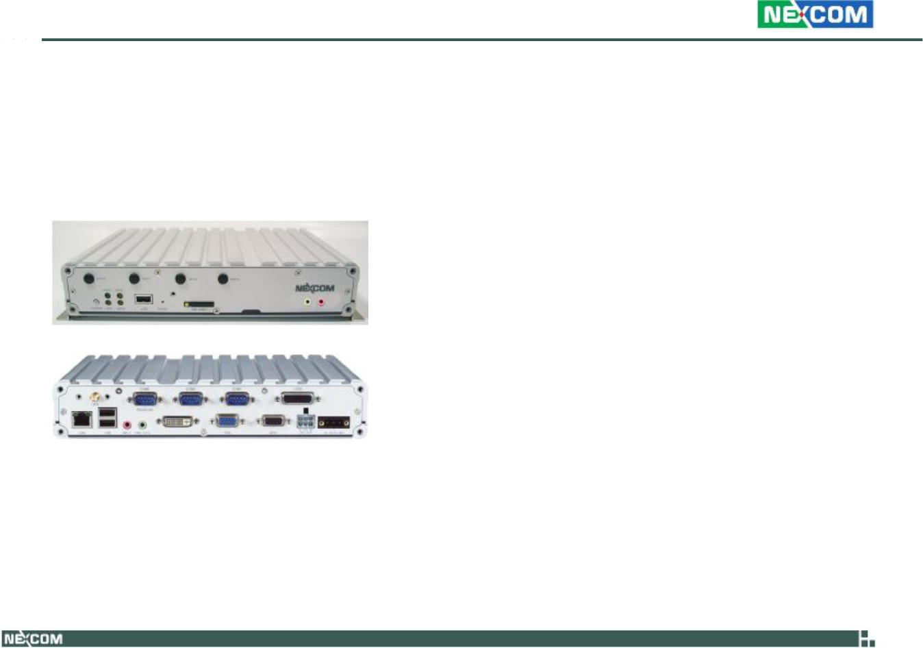
Overview
Front
View
VTC6110
fulfills
vehicle
industry
requirements.
The
design
itself
is
in
compliance
with
vehicle
industrial
standard
such
as
eMark.
More
features
required
for
in-vehicle
operations,
such
as
power
ignition
delay
control,
low-power
protection
and
SMBus
connection,
etc.,
are
continued
from
NEXCOM’s
other
in-vehicle
computer
products.
The
GPS
function
navigates
drivers
to
ultimate
the
fleet
management.
Op-
tional
802.11b/g/n,
3.5G,
GPRS,
and
Bluetooth
availability
make
VTC6110
ready
for
wider
coverage
and
future
trend.
Multiple
display
connections
make
VTC6110
an
ideal
choice
for
in-vehicle
signage
platforms
as
well.
Rear
View
The
VTC6110
is
an
innovative
in-vehicle
computer
for
use
in
any
car,
truck,
or
even
for
maritime
applications.
The
design
itself
makes
the
system
available
as
a
complete
system
allowing
the
user
to
easily
define
and
build
requirements.
Copyright
©
2009
NEXCOM
International
Co.,
Ltd.
All
Rights
Reserved.
1
VTC
6110
User
Manual

Chapter
1:
Product
Introduction
Key
Features
·
Built-in
Intel
®
Core™
Duo
LV
processor
·
Fanless
design
with
ruggedized
aluminum
chassis
·
2
Mini
PCI
Express
and
1
PCI-104
expansions
·
Wide
range
DC
input
from
6V
to
36V
·
Power
ignition
on/off
delay
controlled
by
software
·
Low
battery
power
protection
setting
by
software
·
External
smart
battery
back-up
support
·
S3
&
S4
suspend
mode
support
·
Availability
of
GPS,
GPRS/UMTS/HSDPA
·
Multiple
display
connections
thru
VGA,
DVI-D
and
LVDS
·
Optional
IP65
enclosure
·
e13
Mark
certification
Hardware
Specifications
COM
Express
CPU
Module
(ICES200-L24)
·
Intel
®
Core™
Duo
L2400
·
VGA/PCI/PCIe/LVDS/Audio/COM/LPT/USB2.0/LAN
interface
Memory
·
Supports
DDR2
533/667
non-ECC,
non-registered
SDRAM
·
One
200-pin
SO-DIMM
supports
up
to
2GB
memory
Chipset
·
Intel
945GME
/
ICH7M
Expansion
·
2
Mini
PCI
Express
slots
I/O
Interfaces
-
Front
·
Logo
plate
·
1
x
Power
button
(w/
LED)
·
1
x
Reset
button
·
1
x
SIM
card
socket
·
1
x
USB
2.0
·
1
x
Power
LED
·
1
x
HDD
LED
·
1
x
GPIO
LED
-
programmable
for
alarm
or
other
application
specific
purposes
·
1x
LED
for
COMM
(WLAN/HSDPA)
status
·
Antenna
mounting
holes
for
4x
SMA-type
(WLAN,
HSDPA
and
Blu-
etooth)
·
1
x
Line-out
·
1
x
Mic-in
I/O
Interfaces
-
Rear
·
COM
ports
-
1
x
DB9
COM1
RS232
-
1
x
DB9
COM2
RS232
-
1
x
DB9
COM3
RS232/485
w/
auto
flow
control
·
1
x
DB26
LVDS
(w/
+12V
for
backlight
power
and
USB2.0)
(FOR AT&T NO This Function)
·
1
x
DB15
VGA
·
1
x
DVI-D
·
2
x
USB
·
1
x
Realtek
10/100/1000
Ethernet
·
2
x
Mic-in
and
2
Line-out
(ALC888-VC2-GR
HD
Codec,
AC’97
Compat-
ible)
-
1
x
(PCIe
+
USB)
for
WLAN
card
-
1
x
PCIe
for
HSDPA
module
or
GPRS
module
·
1
PCI-104
slot
·
1
Bluetooth
module
(optional)
Copyright
©
2009
NEXCOM
International
Co.,
Ltd.
All
Rights
Reserved.
2
VTC
6110
User
Manual

Chapter
1:
Product
Introduction
·
6V
(15A)
to
36V
(5A)
thru
DC
3-pin
power
input
connector
(ignition,
power
input
and
ground)
·
1
x
DB9
Female
for
digital
I/O
with
4-input
and
4-output
·
+5
VDC
(1A)
and
+12VDC
(1A)
power
output
and
SMBus
(w/o
VTK
33M-01
connection)
+5
VDC
(0.5A)
and
+12VDC
(0.5A)
power
output
and
SMBus
(w/
VTK
33M-01
connection)
Expandable
Storage
·
1
x
2.5”
SATA
HDD
drive
bay
·
1
Type
II
CompactFlash
socket
(IDE)-
Contruction
·
Aluminum
enclosure
with
fanless
design
Protection
Class
·
IP65
compliant
(w/
optional
IP65
kit)
Certifications
·
CE,
FCC
Class
B,
e13
Mark,
EN50155
Dimensions
·
260mm(W)
x
176mm(D)
x
50mm(H)
(10.24”
x
7”
x
1.97”)
Environment
W/O Vibration Kit
·
Operating
Temperatures:
Ambient
with
air:
-30°C
to
50°C
(CF/SSD);
-30°C
to
50°C
(HDD)
·
Storage
temperature:
-40°C
to
80°C
·
Relative
humidity:
10%
to
90%
(Non-condensing)
·
Vibration
(random):
2g
@
5~500
Hz
with
CF/SSD;
1g
@
5~500
Hz
with
Automotive
HDD
(in
operation)
·
Vibration
Operating:
MIL-STD-810F,
Method
514.5,
Category
20,
Ground
Vehicle
–
Highway
Truck
C-17,
0.04
g2/Hz
at
20-1000
Hz,
-6
dB/Octave
at
1000-2000
Hz
Tested
MIL-STD-810F
method
514.5
Storage:
MIL-STD-810F,
Method
514.5,
Category
24,
Integrity
Test
Shock:
Operating:
MIL-STD-810F,
Method
516.5,
Procedure
I,
Trucks
and
semi-
trailers=20g
Crash
Hazard:
MIL-STD-810F,
Method
516.5,
Procedure
V,
Ground
equipment
=
75g
OS
Support
·
Vista,
XP,
XPe,
Linux
2.6
Copyright
©
2009
NEXCOM
International
Co.,
Ltd.
All
Rights
Reserved.
3
VTC
6110
User
Manual

Chapter
1:
Product
Introduction
Power
Management
·
Power-on
delay
time
is
selectable
by
BIOS
to
disable
and
enable
in
10sec
/
30sec
/
1min
/
5min
/
10
min
/
15min
/
30min
/
1hr.
·
If
the
ignition
is
turned
off
again
and
the
power-on
delay
ended
(in
BIOS
process),
VTC
6110
will
shut
down
immediately.
·
If
VTC
6110
is
off,
only
below
10mA
is
used.
·
Power-off
delay
time
is
selectable
by
BIOS
to
disable
and
enable
in
20sec
/
1min
/
5min
/
10min
/
30min
/
1hr
/
6hr
/
18hr.
·
S3,
S4
suspend
mode
· Ignition On/Off status detectable by SW
· Low battery status detectable by SW
·
Ignition
enable/disable
is
jumper
selectable
·
Shut
down
system
automatically
when
the
system’s
internal
temperature
is
over
80C.
·
VTC
6110
will
automatically
shut
down
5
minutes
after
the
duration
of
low
battery
voltage
is
over
60
sec.
User
can
detect
this
situation
via
software.
·
If
the
ignition
is
off
and
the
system
is
still
on
after
3
minutes,
VTC
6110
will
shut
down
automatically.
·
If
the
ignition
is
off,
the
user
can
detect
this
status
via
the
software.
·
If
the
ignition
is
turned
on
again
and
the
power-off
delay
is
in
progress,
VTC
6110
will
cancel
the
delay
function
and
will
continue
to
operate
normally.
·
If
the
ignition
is
turned
on
again
and
the
power-off
delay
ended,
VTC
6110
will
shut
down
completely
will
power-on
again
automatically.
·
If
the
ignition
is
turned
off
again
and
power-on
delay
is
in
progress,
VTC
6110
will
cancel
the
delay
and
stay
in
power-off
status.
·
If
the
ignition
is
turned
off
again
and
the
power-on
delay
ended
(en-
tered
OS
already),
VTC
6110
will
continue
to
operate
normally.
Copyright
©
2009
NEXCOM
International
Co.,
Ltd.
All
Rights
Reserved.
4
VTC
6110
User
Manual

Chapter 1: Product Introduction
COM
Express
CPU
Module
and
Carrier
Board
The VTC 6110 system uses the ICES200-L24 COM Express CPU module
and the VTCB6110 carrier board.
ICES200-L24
COM
Express
CPU
Module
ICES200-L24 is a COM Express CPU module that uses the Intel® 945GME
chipset and supports Intel® Core™ Duo L2400.
The module also supports one unbuffered non-ECC 533/667 DDR2 SO-
DIMM with maximum memory size up to 2GB. The Intel® 945GME chipset
supports the following interfaces: PCI, PCIe, SATA, VGA, LVDS, LAN, Serial,
USB, etc.
The ICES200-L24 module is based on the COM Express basic form factor
Type 2 standard, x2 connections between the COM Express CPU module
and the I/O carrier board.
The ICES200-L24 CPU module can easily integrate into most of the limited-
space devices such as industrial automation, data acquisition and equip-
ment computers.
VTCB6110
Carrier
Board
Key features:
· Quick customizable COM Express architecture platform
· Wide varieties of built-in communication and I/O ports specially de-
signed for Transport Application
· Customizable delay time for power-on and power-off
· Three external serial port interfaces with two RS232 and one RS232/485
· Supports 10/100/1000 LAN,VGA Console, LVDS and GPIO
· 3 x USB 2.0 ports
· Supports PCI-104 expansion
Copyright
©
2009
NEXCOM
International
Co.,
Ltd.
All
Rights
Reserved.
5
VTC
6110
User
Manual
Chapter
1:
Product
Introduction
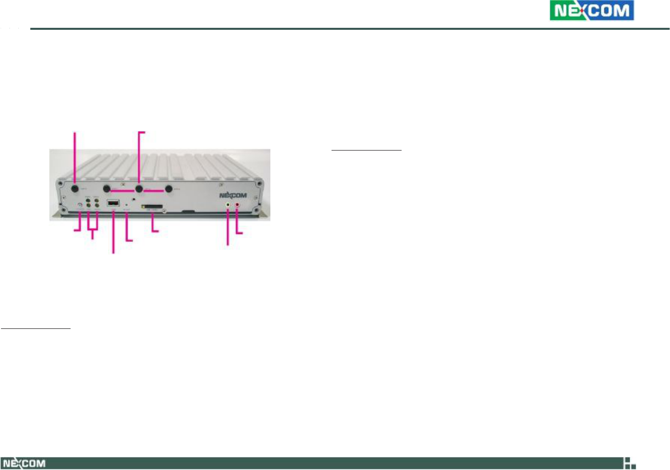
Physical
Features
Front
Panel
GPRS/UMTS/HSDPA
module
antenna
mounting
holes
WiFi/Bluetooth
module
antenna
mounting
holes
2.
Mode
B.
When
the
ignition
is
from
“low”
to
“high”,
you
can
turn
on
VTC
6110
only
by
pressing
the
power
button.
When
the
ignition
is
“high”,
you
can
press
the
power
button
to
turn
on/off
VTC
6110.
If
the
ignition
is
from
“high”
to
“low”,
VTC
6110
will
turn
off
automati-
cally.
When
the
ignition
is
“low”,
pressing
the
power
button
will
not
turn
on
VTC
6110.
Normal PC Mode
3.
Mode
C.
When
there
is
power
input,
you
can
turn
on
VTC
6110
only
by
pressing
the
power
button.
Ignition
signal
will
not
power
on/off
VTC
6110.
4.
Mode
D.
When
there
is
power
input,
VTC
6110
will
turn
on
automati-
cally.
Ignition
signal
will
not
power
on/off
VTC
6110.
Power
button
LEDs
USB
SIM
card
socket
Reset
button
Line-out
Mic-in
Startup
and
Shutdown
Mode
(Refer
to
SW5
setting)
The
start
up
and
shut
down
setting
modes
are
as
follows.
1.
Mode
A
(default
setting).
When
the
input
power
voltage
is
12V,
use
Power
Button
There
are
4
types
of
power
on/off
mode.
Use
JP1
and
JP2
to
select
a
mode.
(refer
to
the
Internal
Jumpers
and
Connectors
section
for
details).
Vehicle PC Mode
1.
Mode
A
(default
setting).
When
the
ignition
is
from
“low”
to
“high”,
VTC
6110
will
turn
on
automatically.
When
the
ignition
is
“high”,
press
SW5
to
select
this
voltage.
Use
the
BIOS
to
select
the
start
up
and
shut
down
voltages.
2.
Mode
B.
When
the
input
power
voltage
is
24V,
use
SW5
to
select
this
voltage.
Use
the
BIOS
to
select
the
start
up
and
shut
down
voltages.
3.
Mode
C.
The
working
input
power
voltage
is
6V~36V.
Start
up
and
shut
down
voltages
settings
are
disabled.
When
using
external
battery
kit
(VTK33B),
mode
C
setting
is
required.
the
power
button
to
turn
on/off
VTC
6110.
When
the
ignition
is
from
“high”
to
“low”,
VTC
6110
will
turn
off
auto-
matically.
When
the
ignition
is
“low”,
pressing
the
power
button
will
not
turn
on
VTC
6110.
Copyright
©
2009
NEXCOM
International
Co.,
Ltd.
All
Rights
Reserved.
6
VTC
6110
User
Manual
Chapter 1: Product Introduction
LEDs
SIM
Card
Socket
VTC 6110 can be internally integrated with a 3.5G Mini Card module. The
SIM card bracket is on the carrier board. When using the GPRS/UMTS/HS-
DPA function, insert the SIM card into the SIM card socket. Make sure to
turn off VTC 6110 before inserting the SIM card.
USB
Port
The USB port complies with USB 2.0 specifications.
WiFi/Bluetooth
Module
Antenna
Mounting
Holes
The 3 external antenna mounting holes are used to mount and connect
WiFi antenna to a WLAN module (Mini Card type).
GPRS/UMTS/HSDPA
Module
Antenna
Mounting
Hole
The antenna mounting hole is used to mount and connect an antenna to
the GPRS/UMTS/HSDPA module.
Reset
Button
Press this button to restart VTC 6110.
Line-out
Line-out is a stereo output for connecting external speakers.
Mic-in
Mic-in receives monophonic input from an external microphone.
Copyright
©
2009
NEXCOM
International
Co.,
Ltd.
All
Rights
Reserved.
7
VTC
6110
User
Manual
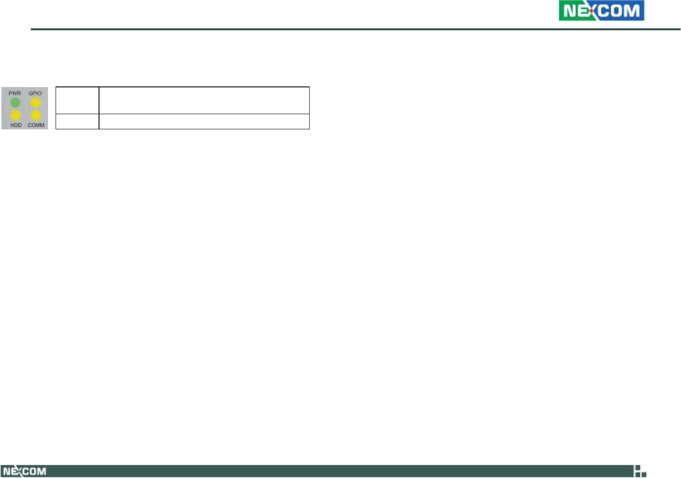
GPIO I/O PORT Address : <Read/Write> #0EE0H Bit 0
:
COMM
WLAN/HSDPA Status
Chapter
1:
Product
Introduction
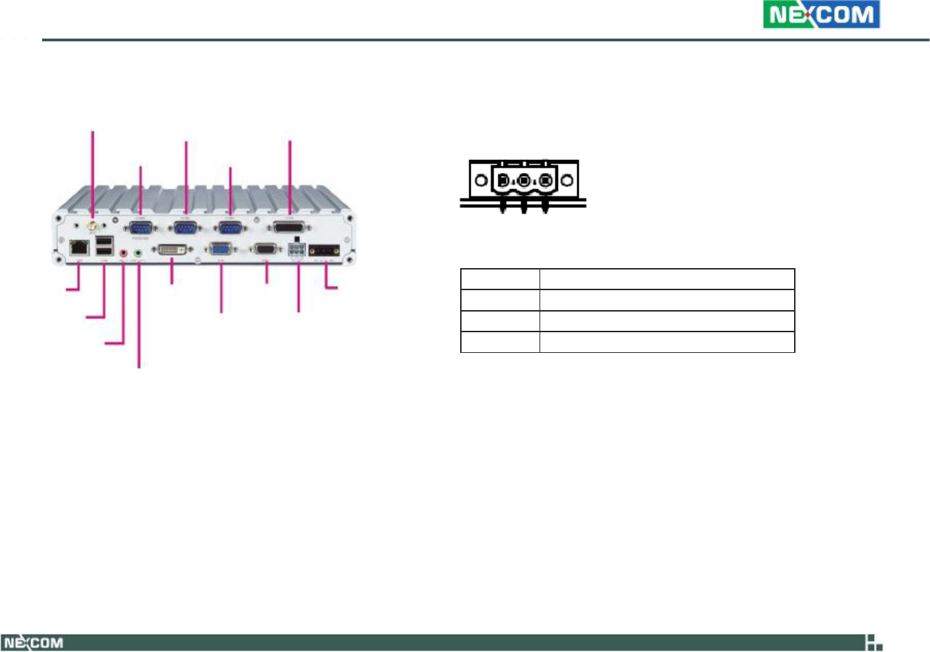
Rear
Panel
Power
Input
GPS
COM3
COM2
COM1
LVDS
DC
Power
Input
Connector
Connector
location
3
2
1
Connector
pin
definition
(CN1)
LAN
DVI-D
GPIO
DC
IN
6V-36V
USB
MIC-IN
LINE-OUT
VGA
5V/12V/SMBUS
**
Use
power
cable
(+)
with
fuse
for
system
protection
Copyright
©
2009
NEXCOM
International
Co.,
Ltd.
All
Rights
Reserved.
8
VTC
6110
User
Manual
Pin
No.
Function
Description
1
GND
2
VIN(6V~36V)
3
IGNITION
Chapter
1:
Product
Introduction
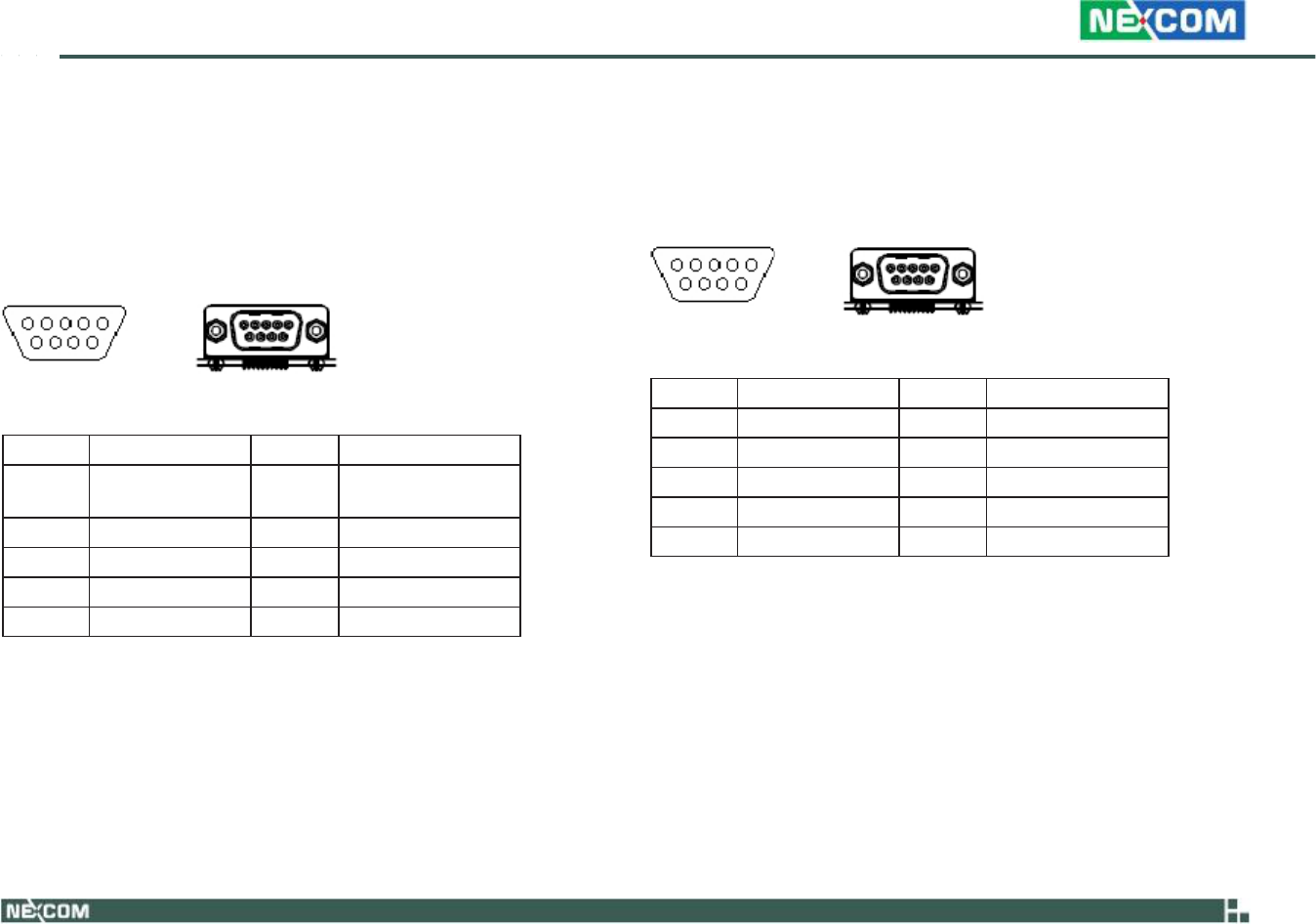
RS232/485
Connector
COM3
The
9
pin
D-Sub
COM
3
port
can
be
configured
as
RS232
or
RS485
using
the
SW6
dip
switch.
Connector
size:
DSUB-9
PIN
Connector
location
RS232
Connector
COM1
and
COM2
Connector
size:
DSUB-9
PIN
Connector
location
1
5
1
5
6
9
6
9
Connector
pin
definition
Connector
pin
definition
Copyright
©
2009
NEXCOM
International
Co.,
Ltd.
All
Rights
Reserved.
9
VTC
6110
User
Manual
PIn
Definition
Pin
Definition
1
DCD
(RS232)
TX-/RX-
(RS485)
2
RXD
(RS232)
TX+/RX+
(RS485)
3
TXD
(RS232)
4
DTR
(RS232)
5
GND
6
DSR
(RS232
)
7
RTS
(RS232)
8
CTS
(RS232)
9
RI
(RS232)
PIn
Definition
Pin
Definition
1
DCD
2
RXD
3
TXD
4
DTR
5
GND
6
DSR
7
RTS
8
CTS
9
RI

Chapter
1:
Product
Introduction
LVDS
Connector
size:
DB-26
PIN
Connector
location
External
SMBus,
12V
and
5V
Power
Output
Connector
location
6
4
3
1
Connector
pin
definition
Connector
pin
definition
+5
VDC
(1A)
and
+12VDC
(1A)
power
output
and
SMBus
(w/o
VTK
33M-01
connection)
+5
VDC
(0.5A)
and
+12VDC
(0.5A)
power
output
and
SMBus
(w/
VTK
33M-01
connection)
SM BUS No this function (for Engineering use)
No this function (for Engineering use)
Copyright
©
2009
NEXCOM
International
Co.,
Ltd.
All
Rights
Reserved.
10
VTC
6110
User
Manual
Pin
Definition
Pin
Definition
1
Panel_
EN
2
Panel_control
3
VDD
4
VDD
5
LCDD09(OUT3)
6
LCDD01(OUT0)
7
LCDD08(OUT3#)
8
LCDD00(OUT0#)
9
LCDD_GND
10
LCDD_GND
11
LCDD07(CLK)
12
LCDD03(OUT1)
13
LCDD06(CLK#)
14
LCDD02(OUT1#)
15
LVDS_GND
16
LCDD_GND
17
LCDD05(OUT2)
18
Power
on
push
button
19
LCDD04(OUT2#)
20
Panel_backlight
21
LCDD_GND
22
Panel-Gnd
23
USB_0#
24
Contact_DET#
25
USB_0
26
USB_VCC
PIn
Definition
Pin
Definition
1
5V
2
12V
3
SMBus
Clock
4
GND
5
GND
6
SMBus
Data

Chapter 1: Product Introduction
VGA
Port
The DB15 VGA port supports resolutions up to 1600x1200 @ 85 Hz,
2048x1536 @ 60Hz.
USB
Port
x
2
The two USB ports are compliant with USB 2.0 specifications.
LAN
Port
The LAN port is an RJ45 interface with integrated LEDs and supports
10/100/1000Mbps Ethernet data transfer rates.
Audio
Jacks
(MIC-IN
and
LINE-OUT)
· MIC-IN jack receives monophonic input from an external microphone.
· LINE-OUT jack is the stereo output for connecting external speakers.
Copyright
©
2009
NEXCOM
International
Co.,
Ltd.
All
Rights
Reserved.
11
VTC
6110
User
Manual

50.0
Chapter
1:
Product
Introduction
Mechanical
Dimensions
260.0
176.0
Copyright
©
2009
NEXCOM
International
Co.,
Ltd.
All
Rights
Reserved.
12
VTC
6110
User
Manual

Chapter
2:
Jumpers
and
Connectors
C
HAPTER
2:
J
UMPERS
AND
C
ONNECTORS
This
chapter
describes
how
to
set
the
jumpers
on
the
motherboard.
Note
that
the
following
procedures
are
generic
for
all
VTC
6110
series.
Before
You
Begin
·
Ensure
you
have
a
stable,
clean
working
environment.
Dust
and
dirt
can
get
into
components
and
cause
a
malfunction.
Use
containers
to
keep
small
components
separated.
·
Adequate
lighting
and
proper
tools
can
prevent
you
from
accidentally
damaging
the
internal
components.
Most
of
the
procedures
that
follow
require
only
a
few
simple
tools,
including
the
following:
·
A
Philips
screwdriver
·
A
flat-tipped
screwdriver
·
A
set
of
jewelers
Screwdrivers
·
A
grounding
strap
·
An
anti-static
pad
·
Using
your
fingers
can
disconnect
most
of
the
connections.
It
is
recom-
mended
that
you
do
not
use
needle-nosed
pliers
to
disconnect
connec-
tions
as
these
can
damage
the
soft
metal
or
plastic
parts
of
the
connec-
tors.
·
Before
working
on
internal
components,
make
sure
that
the
power
is
off.
Ground
yourself
before
touching
any
internal
components,
by
touching
a
metal
object.
Static
electricity
can
damage
many
of
the
elec-
Copyright
©
2009
NEXCOM
International
Co.,
Ltd.
All
Rights
Reserved.
13
tronic
components.
Humid
environment
tend
to
have
less
static
electric-
ity
than
dry
environments.
A
grounding
strap
is
warranted
whenever
danger
of
static
electricity
exists.
Precautions
Computer
components
and
electronic
circuit
boards
can
be
damaged
by
discharges
of
static
electricity.
Working
on
the
computers
that
are
still
con-
nected
to
a
power
supply
can
be
extremely
dangerous.
Follow
the
guidelines
below
to
avoid
damage
to
your
computer
or
your-
self:
·
Always
disconnect
the
unit
from
the
power
outlet
whenever
you
are
working
inside
the
case.
·
If
possible,
wear
a
grounded
wrist
strap
when
you
are
working
inside
the
computer
case.
Alternatively,
discharge
any
static
electricity
by
touching
the
bare
metal
chassis
of
the
unit
case,
or
the
bare
metal
body
of
any
other
grounded
appliance.
·
Hold
electronic
circuit
boards
by
the
edges
only.
Do
not
touch
the
com-
ponents
on
the
board
unless
it
is
necessary
to
do
so.
Don’t
flex
or
stress
the
circuit
board.
·
Leave
all
components
inside
the
static-proof
packaging
that
they
shipped
with
until
they
are
ready
for
installation.
·
Use
correct
screws
and
do
not
over
tighten
screws.
VTC
6110
User
Manual
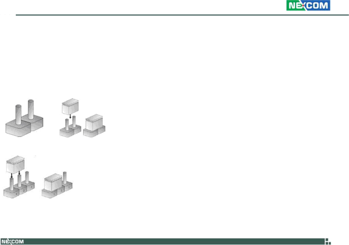
Chapter
2:
Jumpers
and
Connectors
Jumper
A
jumper
is
the
simplest
kind
of
electric
switch.
It
consists
of
two
metal
pins
and
a
cap.
When
setting
the
jumpers,
ensure
that
the
jumper
caps
are
placed
on
the
correct
pins.
When
the
jumper
cap
is
placed
on
both
pins,
the
jumper
is
short
.
If
you
remove
the
jumper
cap,
or
place
the
jumper
cap
on
just
one
pin,
the
jumper
is
open
.
Refer
to
the
illustrations
below
for
examples
of
what
the
2-pin
and
3-pin
jumpers
look
like
when
they
are
short
(on)
and
open
(off).
Two-Pin
Jumpers:
Open
(Left)
and
Short
(Right)
Three-Pin
Jumpers:
Pins
1
and
2
Are
Short
Copyright
©
2009
NEXCOM
International
Co.,
Ltd.
All
Rights
Reserved.
14
VTC
6110
User
Manual
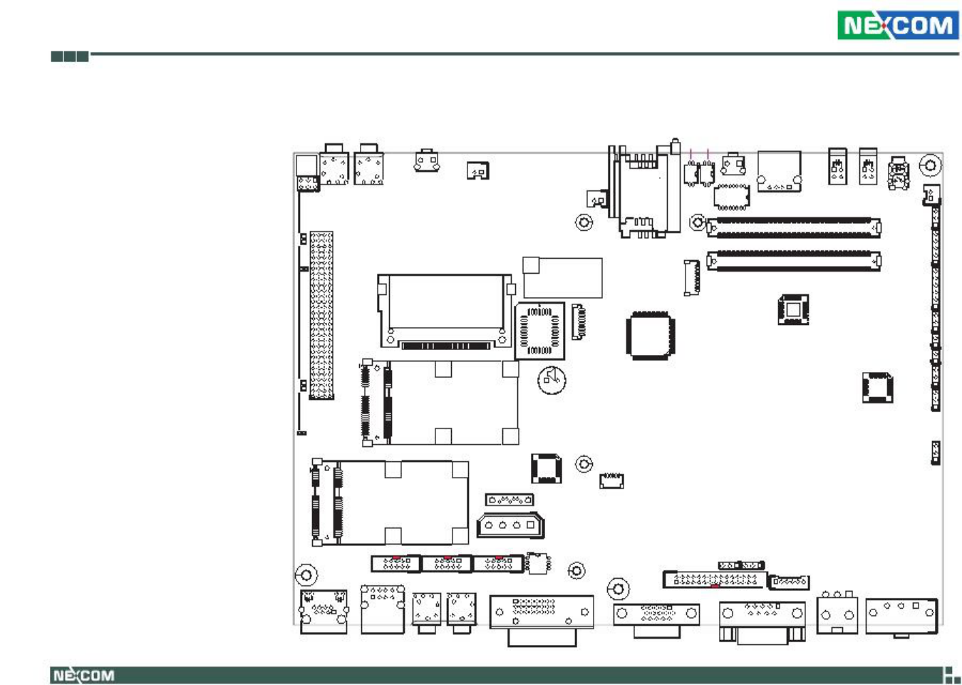
10
Chapter
2:
Jumpers
and
Connectors
Locations
of
the
Jumpers
and
Connectors
VTCB6110
SW5SW4
SW2
The
figure
on
the
right
is
the
VTCB6110
carrier
board
which
is
the
board
used
in
the
VTC6110
system.
It
shows
the
loca-
tions
of
the
jumpers
and
connectors.
J13
CN15
CN14
SW7
J11
J9
SW3
USB1
J4
LED2
LED1
SW1
J2
J1
CN17
CN4
JP6
J12
Blue
Tooth
J7
J3
JP5
JP4
J14
JP8
JP7
JP3
CN16
3.5G
BZ1
JP2
JP1
WLAN
CN6
J10
J8
CN12
CN9
CN7
SW6
J6
J5
LAN1
USB2
CN11
CN8
CN5
CON1
COM1
CN2
CN1
Copyright
©
2009
NEXCOM
International
Co.,
Ltd.
All
Rights
Reserved.
15
VTC
6110
User
Manual

Chapter
2:
Jumpers
and
Connectors
Jumper
Settings
LVDS
Power
Input
Voltage
Select
(JP9)
SW5:
Input
Voltage
Selection
CMOS
Input
Voltage
Select
(J6)
SW6:
COM
Port
Mode
Selection
BIOS
Function
Select
(J1)
CF
(IDE0)
Primary
Master/Slave
Select
(JP4)
Copyright
©
2009
NEXCOM
International
Co.,
Ltd.
All
Rights
Reserved.
16
DC
Input
Voltage
Select
(JP1)
VTC
6110
User
Manual
SW6
COM
Port
Mode
RS232
(default)
RS485
SW6.1
OFF
ON
SW6.2
OFF
ON
SW6.3
OFF
ON
SW5
/
Input
Voltage
12V
(default)
24V
6V~36V
SW5.1
OFF
OFF
ON
SW5.2
OFF
ON
Ignore
Pin
Status
Function
Description
1-2
Short
Disable
carrier
board
BIOS
2-3
(default)
Short
(default)
Disable
module
board
BIOS
Pin
Status
Function
Description
1-2
Short
Slave
2-3
(default)
Short
(default)
Master
Pin
Status
Function
Description
1-2
Short
+5V
IN
2-3
(default)
Short
(default)
+3.3V
IN
Pin
Status
Function
Description
1-2
(default)
Short
(default)
VBAT
IN
2-3
Short
Clear
CMOS
Pin
Status
Function
Description
1-2
(default)
Short
(default)
IGNITION
2-3
Short
VIN_M

Chapter
2:
Jumpers
and
Connectors
Temp
Sensor
(JP8)
GAL
Download
(JP5)
Auto
Power
Select
(JP2)
MCU
COM
Port
(JP3)
PCI-104
VI/O
Select
Voltage
(J13)
MCU
Download
(JP6)
Copyright
©
2009
NEXCOM
International
Co.,
Ltd.
All
Rights
Reserved.
17
VTC
6110
User
Manual
Pin
Function
Description
1
+V3.3S
2
GND
3
TCK
4
TDO
5
TDI
6
TMS
Pin
Function
Description
1
+V3.3ALW
2
C2D
3
MRST
4
C2CK
5
GND
Pin
Function
Description
1
TX
2
RX
3
GND
Pin
Status
Function
Description
1-4(*)
Short*
+3.3V
3-6
Short
+5V
Pin
Function
Description
1
SENSOR+
2
GND
Pin
Status
Function
Description
1-2
(default)
Short
(default)
AUTO
2-3
Short
BUTTON
CONTROL
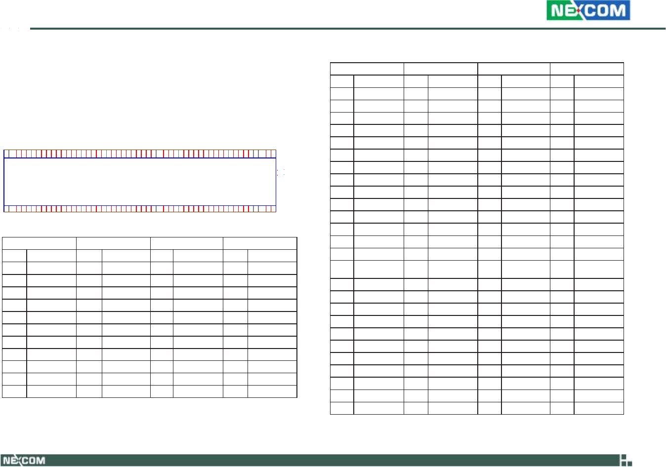
B1
B2
B3
B4
B5
B6
B7
B8
B9
B10
B11
B12
B13
B14
B15
B16
B17
B18
B19
B20
B21
B22
B23
B24
B25
B26
B27
B28
B29
B30
B31
B32
B33
B34
B35
B36
B37
B38
B39
B40
B41
B42
B43
B44
B45
B46
B47
B48
B49
B50
B51
B52
B53
B54
B55
B56
B57
B58
B59
B60
B61
B62
B63
B64
B65
B66
B67
B68
B69
B70
B71
B72
B73
B74
B75
B
76
B77
B78
B79
B80
B81
B82
B83
B84
B85
B86
B87
B88
B89
B90
B91
B92
B93
B94
B95
B96
B97
B98
B99
B100
B101
B102
B103
B104
B105
B106
B107
B108
B109
B110
B1
B2
B3
B4
B5
B6
B7
B8
B9
B10
B11
B12
B13
B14
B15
B16
B17
B18
B19
B20
B21
B22
B23
B24
B25
B26
B27
B28
B29
B30
B31
B32
B33
B34
B35
B36
B37
B38
B39
B40
B41
B42
B43
B44
B45
B46
B47
B48
B49
B50
B51
B52
B53
B54
B55
B56
B57
B58
B59
B60
B61
B62
B63
B64
B65
B66
B67
B
68
B69
B70
B71
B72
B73
B74
B75
B76
B77
B78
B79
B80
B81
B82
B83
B84
B85
B86
B87
B88
B89
B90
B91
B92
B93
B94
B95
B96
B97
B98
B99
B100
B101
B102
B103
B104
B105
B106
B107
B108
B109
B110
A1
A2
A3
A4
A5
A6
A7
A8
A9
A10
A11
A12
A13
A14
A15
A16
A17
A18
A19
A20
A21
A22
A23
A24
A25
A26
A27
A28
A29
A30
A31
A32
A33
A34
A35
A36
A37
A38
A39
A40
A41
A42
A43
A44
A45
A46
A47
A48
A49
A50
A51
A52
A53
A54
A55
A56
A57
A58
A59
A
60
A61
A62
A63
A64
A65
A66
A67
A68
A69
A70
A71
A72
A73
A74
A75
A76
A77
A78
A79
A80
A81
A82
A83
A84
A85
A86
A87
A88
A89
A90
A91
A92
A93
A94
A95
A96
A97
A98
A99
A100
A101
A102
A103
A104
A105
A106
A107
A108
A10
9
A110
A1
A2
A3
A4
A5
A6
A7
A8
A9
A10
A11
A12
A13
A14
A15
A16
A17
A18
A19
A20
A21
A22
A23
A24
A25
A26
A27
A28
A29
A30
A31
A32
A33
A34
A35
A36
A37
A38
A39
A40
A41
A42
A43
A44
A45
A46
A47
A48
A49
A50
A51
A
52
A53
A54
A55
A56
A57
A58
A59
A60
A61
A62
A63
A64
A65
A66
A67
A68
A69
A70
A71
A72
A73
A74
A75
A76
A77
A78
A79
A80
A81
A82
A83
A84
A85
A86
A87
A88
A89
A90
A91
A92
A93
A94
A95
A96
A97
A98
A99
A100
A101
A102
A103
A104
A105
A106
A107
A108
A109
A110
Chapter
2:
Jumpers
and
Connectors
Connectors
High
Speed
Board-to-Board
Connector:
COM
Express
Row
A
and
Row
B
Connector
size:
2
x
110
=
220
pins
Connector
location:
J4
J1
C OM E xp re ss
MH 2
MH 1
Connector
Pin
Definition
Copyright
©
2009
NEXCOM
International
Co.,
Ltd.
All
Rights
Reserved.
18
VTC
6110
User
Manual
Row
A
Row
B
Row
A
Row
B
A13
GBE0_MDI0+
B13
SMB_CK
A68
PCIE_TX0+
B68
PCIE_RX0+
A14
GBE0_CTREF
B14
SMB_DAT
A69
PCIE_TX0-
B69
PCIE_RX0-
A15
SUS_S3#
B15
SMB_ALERT#
A70
GND
B70
GND
A16
SATA0_TX+
B16
NC
A71
LVDS_A0+
B71
NC
A17
SATA0_TX-
B17
NC
A72
LVDS_A0-
B72
NC
A18
SUS_S4#
B18
SUS_STAT#
A73
LVDS_A1+
B73
NC
A19
SATA0_RX+
B19
NC
A74
LVDS_A1+
B74
NC
A20
SATA0_RX-
B20
NC
A75
LVDS_A2+
B75
NC
A21
GND
B21
GND
A76
LVDS_A2+
B76
NC
A22
NC
B22
NC
A77
LVDS_VDD_EN
B77
NC
A23
NC
B23
NC
A78
LVDS_A3+
B78
NC
A24
SUS_S5#
B24
PWR_OK
A79
LVDS_A3+
B79
LVDS_BKLT_EN
A25
NC
B25
NC
A80
GND
B80
GND
A26
NC
B26
NC
A81
LVDS_A_CK+
B81
NC
A27
BATLOW#
B27
NC
A82
LVDS_A_CK-
B82
NC
A28
ATA_ACT#
B28
NC
A83
LVDS_I2C_CK
B83
LVDS_BKLT_
CTRL
A29
AC_SYNC
B29
NC
A84
LVDS_I2C_DAT
B84
VCC_5V_SBY
A30
AC_RST#
B30
AC_SDIN0
A85
NC
B85
VCC_5V_SBY
A31
GND
B31
GND
A86
NC
B86
VCC_5V_SBY
A32
AC_BITCLK
B32
SPKR
A87
NC
B87
VCC_5V_SBY
A33
AC_SDOUT
B33
I2C_CK
A88
PCIE0_CK_REF+
B88
RSVD
A34
NC
B34
I2C_DAT
A89
PCIE0_CK_REF-
B89
NC
A35
NC
B35
THRM#
A90
GND
B90
GND
A36
USB6-
B36
NC
A91
RSVD
B91
NC
A37
USB6+
B37
NC
A92
RSVD
B92
NC
A38
USB_6_7_OC#
B38
USB_4_5_OC#
A93
NC
B93
NC
A39
USB4-
B39
USB5-
A94
RSVD
B94
NC
Row
A
Row
B
Row
A
Row
B
A1
GND
B1
GND
A56
NC
B56
NC
A2
GBE0_MDI3-
B2
GBE0_ACT#
A57
GND
B57
NC
A3
GBE0_MDI3+
B3
LPC_FRAME#
A58
NC
B58
NC
A4
NC
B4
LPC_AD0
A59
NC
B59
NC
A5
NC
B5
LPC_AD1
A60
GND
B60
GND
A6
GBE0_MDI2-
B6
LPC_AD2
A61
NC
B61
NC
A7
GBE0_MDI2+
B7
LPC_AD3
A62
NC
B62
NC
A8
GBE0_LINK#
B8
NC
A63
GPI1
B63
GPO3
A9
GBE0_MDI1-
B9
NC
A64
NC
B64
NC
A10
GBE0_MDI1+
B10
LPC_CLK
A65
NC
B65
NC
A11
GND
B11
GND
A66
GND
B66
NC
A12
GBE0_MDI0-
B12
PWRBTN#
A67
NC
B67
NC
Row
B
MH 2
MH
1
COM
Express
Connector
Row
A

Chapter
2:
Jumpers
and
Connectors
Copyright
©
2009
NEXCOM
International
Co.,
Ltd.
All
Rights
Reserved.
19
VTC
6110
User
Manual
Row
A
Row
B
Row
A
Row
B
A40
USB4+
B40
USB5+
A95
RSVD
B95
NC
A41
GND
B41
GND
A96
GND
B96
NC
A42
USB2-
B42
USB3-
A97
VCC_12V
B97
NC
A43
USB2+
B43
USB3+
A98
VCC_12V
B98
NC
A44
USB_2_3_OC#
B44
USB_0_1_OC#
A99
VCC_12V
B99
NC
A45
USB0-
B45
USB1-
A100
GND
B100
GND
A46
USB0+
B46
USB1+
A101
VCC_12V
B101
VCC_12V
A47
VCC_RTC
B47
NC
A102
VCC_12V
B102
VCC_12V
A48
NC
B48
NC
A103
VCC_12V
B103
VCC_12V
A49
NC
B49
SYS_RESET#
A104
VCC_12V
B104
VCC_12V
A50
NC
B50
CB_RESET#
A105
VCC_12V
B105
VCC_12V
A51
GND
B51
GND
A106
VCC_12V
B106
VCC_12V
A52
NC
B52
NC
A107
VCC_12V
B107
VCC_12V
A53
NC
B53
NC
A108
VCC_12V
B108
VCC_12V
A54
NC
B54
NC
A109
VCC_12V
B109
VCC_12V
A55
NC
B55
NC
A110
GND
B110
GND
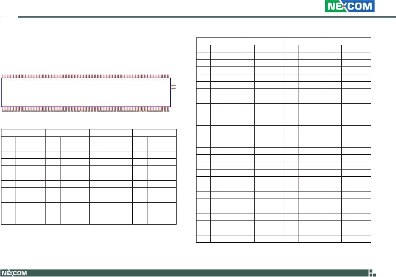
B1
B2
B3
B4
B5
B6
B7
B8
B9
B10
B11
B12
B13
B14
B15
B16
B17
B18
B19
B20
B21
B22
B23
B24
B25
B26
B27
B28
B29
B30
B31
B32
B33
B34
B35
B36
B37
B38
B39
B40
B41
B
42
B43
B44
B45
B46
B47
B48
B49
B50
B51
B52
B53
B54
B55
B56
B57
B58
B59
B60
B61
B62
B63
B64
B65
B66
B67
B68
B69
B70
B71
B72
B73
B74
B75
B76
B77
B78
B79
B80
B81
B82
B83
B84
B85
B86
B87
B88
B89
B90
B91
B92
B9
3
B94
B95
B96
B97
B98
B99
B100
B101
B102
B103
B104
B105
B106
B107
B108
B109
B110
B1
B2
B3
B4
B5
B6
B7
B8
B9
B10
B11
B12
B13
B14
B15
B16
B17
B18
B19
B20
B21
B22
B23
B24
B25
B26
B27
B28
B29
B30
B31
B32
B33
B
34
B35
B36
B37
B38
B39
B40
B41
B42
B43
B44
B45
B46
B47
B48
B49
B50
B51
B52
B53
B54
B55
B56
B57
B58
B59
B60
B61
B62
B63
B64
B65
B66
B67
B68
B69
B70
B71
B72
B73
B74
B75
B76
B77
B78
B79
B80
B81
B82
B83
B84
B8
5
B86
B87
B88
B89
B90
B91
B92
B93
B94
B95
B96
B97
B98
B99
B100
B101
B102
B103
B104
B105
B106
B107
B108
B109
B110
A1
A2
A3
A4
A5
A6
A7
A8
A9
A10
A11
A12
A13
A14
A15
A16
A17
A18
A19
A20
A21
A22
A23
A24
A25
A
26
A27
A28
A29
A30
A31
A32
A33
A34
A35
A36
A37
A38
A39
A40
A41
A42
A43
A44
A45
A46
A47
A48
A49
A50
A51
A52
A53
A54
A55
A56
A57
A58
A59
A60
A61
A62
A63
A64
A65
A66
A67
A68
A69
A70
A71
A72
A73
A74
A75
A76
A7
7
A78
A79
A80
A81
A82
A83
A84
A85
A86
A87
A88
A89
A90
A91
A92
A93
A94
A95
A96
A97
A98
A99
A100
A101
A102
A103
A104
A105
A106
A107
A108
A109
A110
A1
A2
A3
A4
A5
A6
A7
A8
A9
A10
A11
A12
A13
A14
A15
A16
A17
A
18
A19
A20
A21
A22
A23
A24
A25
A26
A27
A28
A29
A30
A31
A32
A33
A34
A35
A36
A37
A38
A39
A40
A41
A42
A43
A44
A45
A46
A47
A48
A49
A50
A51
A52
A53
A54
A55
A56
A57
A58
A59
A60
A61
A62
A63
A64
A65
A66
A67
A68
A6
9
A70
A71
A72
A73
A74
A75
A76
A77
A78
A79
A80
A81
A82
A83
A84
A85
A86
A87
A88
A89
A90
A91
A92
A93
A94
A95
A96
A97
A98
A99
A100
A101
A102
A103
A104
A105
A106
A107
A108
A109
A110
Chapter
2:
Jumpers
and
Connectors
High
Speed
Board-to-Board
Connector:
COM
Express
Row
C
and
Row
D
Connector
size:
2
X
110
=
220
Pins
Connector
location:
J3
J1
C OM E xp re ss
Row
D
COM
Express
Connector
MH2
MH2
MH1
MH1
Row
C
Connector
Pin
Definition
Copyright
©
2009
NEXCOM
International
Co.,
Ltd.
All
Rights
Reserved.
20
VTC
6110
User
Manual
Row
C
Row
D
Row
C
Row
D
C13
IDE_IORDY
D13
IDE_A0
C68
NC
D68
NC
C14
IDE_IOR#
D14
IDE_A1
C69
NC
D69
NC
C15
NC
D15
IDE_A2
C70
GND
D70
GND
C16
NC
D16
IDE_CS1#
C71
NC
D71
NC
C17
NC
D17
IDE_CS3#
C72
NC
D72
NC
C18
NC
D18
IDE_RESET#
C73
NC
D73
SDVO_CLK
C19
NC
D19
NC
C74
NC
D74
NC
C20
PCI_GNT0#
D20
NC
C75
NC
D75
NC
C21
GND
D21
GND
C76
GND
D76
GND
C22
PCI_REQ0#
D22
PCI_AD1
C77
NC
D77
IDE_CBLID#
C23
PCI_RESET#
D23
PCI_AD3
C78
NC
D78
NC
C24
PCI_AD0
D24
PCI_AD5
C79
NC
D79
NC
C25
PCI_AD2
D25
PCI_AD7
C80
GND
D80
GND
C26
PCI_AD4
D26
PCI_C/BE0#
C81
NC
D81
NC
C27
PCI_AD6
D27
PCI_AD9
C82
NC
D82
NC
C28
PCI_AD8
D28
PCI_AD11
C83
NC
D83
NC
C29
PCI_AD10
D29
PCI_AD13
C84
GND
D84
GND
C30
PCI_AD12
D30
PCI_AD15
C85
NC
D85
NC
C31
GND
D31
GND
C86
NC
D86
NC
C32
PCI_AD14
D32
PCI_PAR
C87
GND
D87
GND
C33
PCI_C/BE1#
D33
PCI_SERR#
C88
NC
D88
NC
C34
PCI_PERR#
D34
PCI_STOP#
C89
NC
D89
NC
C35
PCI_LOCK#
D35
PCI_TRDY#
C90
GND
D90
GND
C36
PCI_DEVSEL#
D36
PCI_FRAME#
C91
NC
D91
NC
C37
PCI_IRDY#
D37
PCI_AD16
C92
NC
D92
NC
C38
PCI_C/BE2#
D38
PCI_AD18
C93
GND
D93
GND
C39
PCI_AD17
D39
PCI_AD20
C94
NC
D94
NC
Row
C
Row
D
Row
C
Row
D
C1
GND
D1
GND
C56
NC
D56
SDVOB_GREEN-
C2
IDE_D7
D2
IDE_D5
C57
NC
D57
NC
C3
IDE_D6
D3
IDE_D10
C58
NC
D58
SDVOB_BLUE+
C4
IDE_D3
D4
IDE_D11
C59
NC
D59
SDVOB_BLUE-
C5
IDE_D15
D5
IDE_D12
C60
GND
D60
GND
C6
IDE_D8
D6
IDE_D4
C61
NC
D61
SDVO_CLK+
C7
IDE_D9
D7
IDE_D0
C62
NC
D62
SDVO_CLK-
C8
IDE_D2
D8
IDE_REQ
C63
NC
D63
NC
C9
IDE_D13
D9
IDE_IOW#
C64
NC
D64
NC
C10
IDE_D1
D10
IDE_ACK#
C65
NC
D65
NC
C11
GND
D11
GND
C66
NC
D66
NC
C12
IDE_D14
D12
IDE_IRQ
C67
NC
D67
GND

Chapter
2:
Jumpers
and
Connectors
Copyright
©
2009
NEXCOM
International
Co.,
Ltd.
All
Rights
Reserved.
21
VTC
6110
User
Manual
Row
C
Row
D
Row
C
Row
D
C40
PCI_AD19
D40
PCI_AD22
C95
PEG_RX13-
D95
PEG_TX13-
C41
GND
D41
GND
C96
GND
D96
GND
C42
PCI_AD21
D42
PCI_AD24
C97
RSVD
D97
PEG_ENABLE#
C43
PCI_AD23
D43
PCI_AD26
C98
PEG_RX14+
D98
PEG_TX14+
C44
PCI_C/BE3#
D44
PCI_AD28
C99
PEG_RX14-
D99
PEG_TX14-
C45
PCI_AD25
D45
PCI_AD30
C100
GND
D100
GND
C46
PCI_AD27
D46
PCI_IRQC#
C101
PEG_RX15+
D101
PEG_TX15+
C47
PCI_AD29
D47
PCI_IRQD#
C102
PEG_RX15-
D102
PEG_TX15-
C48
PCI_AD31
D48
PCI_CLKRUN#
C103
GND
D103
GND
C49
PCI_IRQA#
D49
PCI_M66EN
C104
VCC_12V
D104
VCC_12V
C50
PCI_IRQB#
D50
PCI_CLK
C105
VCC_12V
D105
VCC_12V
C51
GND
D51
GND
C106
VCC_12V
D106
VCC_12V
C52
PEG_RX0+
D52
PEG_TX0+
C107
VCC_12V
D107
VCC_12V
C53
PEG_RX0-
D53
PEG_TX0-
C108
VCC_12V
D108
VCC_12V
C54
TYPE0#
D54
PEG_LANE_RV#
C109
VCC_12V
D109
VCC_12V
C55
PEG_RX1+
D55
PEG_TX1+
C110
GND
D110
GND

49
Chapter
2:
Jumpers
and
Connectors
CompactFlash
Connector
Connector
size:
2
x
25
=
50
pins
Connector
location:
J12
50
26
1
Connector
Pin
Definition
Copyright
©
2009
NEXCOM
International
Co.,
Ltd.
All
Rights
Reserved.
22
VTC
6110
User
Manual
Pin
Description
Pin
Description
23
Data
2
24
IOCS16#
(NC)
25
CF_CD2#
(Pull-down)
26
CF_CD1#
(Pull-down)
27
Data
11
28
Data
12
29
Data
13
30
Data
14
31
Data
15
32
HDC
CS300
33
CF_VS1#
(NC)
34
IOR
35
IOW
36
CF_WE#
(+5V)
37
Interrupt
15
38
+5V
39
CF_CSEL#
(Master
or
Slave)
40
CF_VS2#
(NC)
41
Reset
#
42
IOCHRDY
43
DMA
REQ
/
DACK
(NC)
44
DMA
ACK#
/CF_REG#
(+5V)
45
HDD
Active
Led
46
DMA66
Detect
/
CF_PDIAG#
47
Data
8
48
Data
9
49
Data
10
50
Gnd
Pin
Description
Pin
Description
1
Gnd
2
Data
3
3
Data
4
4
Data
5
5
Data
6
6
Data
7
7
HDC
CS100
8
Gnd
9
Gnd
10
Gnd
11
Gnd
12
Gnd
13
+5V
14
Gnd
15
Gnd
16
Gnd
17
Gnd
18
Disk
Address
2
19
Disk
Address
1
20
Disk
Address
0
21
Data
0
22
Data
1
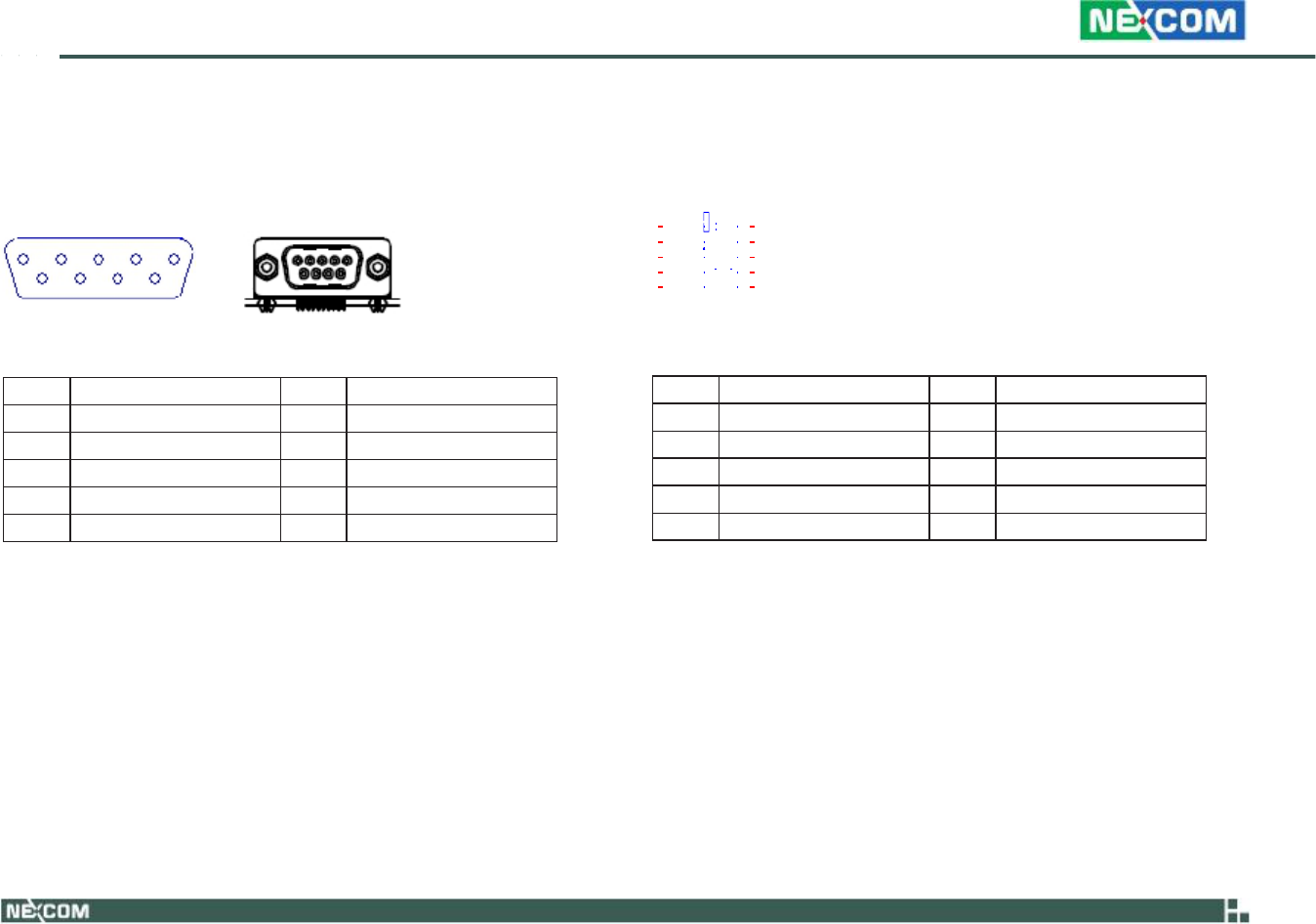
3 42
Chapter
2:
Jumpers
and
Connectors
GPIO
Connector
Connector
size:
DSUB-9
pin
Connector
location:
COM1
5
1
9
6
Connector
Pin
Definition
Copyright
©
2009
NEXCOM
International
Co.,
Ltd.
All
Rights
Reserved.
23
RS232
Connector:
COM1,
COM2
Connector
size:
2
x
10
=
20
Pins
Pin
Header,
(2.0
mm
Pitch)
Connector
location:
COM1
(CN9),
COM2
(CN7)
CN10
1
5
6
7
8
9
10
BOX-2.0mm-M-180
Connector
Pin
Definition
VTC
6110
User
Manual
Pin
Description
Pin
Description
1
GIN1
2
GIN2
3
GIN3
4
GIN4
5
GOUT4
6
GOUT1
7
GOUT2
8
GOUT3
9
GND
Pin
Definition
Pin
Definition
1
DCD
2
RXD
3
TXD
4
DTR
5
Gnd
6
DSR
7
RTS
8
CTS
9
RI
3 42
Chapter
2:
Jumpers
and
Connectors
RS232/485
Connector:
COM3
Connector
size:
2
x
10
=
20
Pins
Pin
Header,
(2.0
mm
Pitch)
Connector
location:
CN12
GAL
Programmer
PIN
Header
Connector
size:
2.54mm-M-180
Connector
location:
JP5
CN10
1
5
6
7
8
9
10
BOX-2.0mm-M-180
1
2
3
4
5
6
JP5
PIN-2.54mm-M-180
Connector
Pin
Definition
Copyright
©
2009
NEXCOM
International
Co.,
Ltd.
All
Rights
Reserved.
24
Connector
Pin
Definition
VTC
6110
User
Manual
Pin
Definition
Pin
Definition
1
DCD
(RS232)
TX-/RX-
(RS485)
2
RXD
(RS232)
TX+/RX+
(RS485)
3
TXD
(RS232)
4
DTR
(RS232)
5
Gnd
6
DSR
(RS232)
7
RTS
(RS232)
8
CTS
(RS232)
9
RI
(RS232)
Pin
Definition
Pin
Definition
1
+3.3V
2
GND
3
TCK
4
TDO
5
TDI
6
TMS

Chapter
2:
Jumpers
and
Connectors
MCU
Programmer
Pin
Header
Connector
size:
2.54mm-M-180
Connector
location:
JP6
VGA
Connector
Connector
size:
DSUB-15
Connector
location:
CON1
1
2
3
4
5
JP6
PIN-2.54mm-M-180
Connector
Pin
Definition
Copyright
©
2009
NEXCOM
International
Co.,
Ltd.
All
Rights
Reserved.
25
Connector
Pin
Definition
VTC
6110
User
Manual
Pin
Definition
Pin
Definition
1
RED
2
GREEN
3
BLUE
4
NC
5
Gnd
6
Gnd
7
Gnd
8
Gnd
9
VCC
10
Gnd
11
NC
12
DDCDAT
13
Hsync
14
Vsync
15
DDCCLK
Pin
Definition
Pin
Definition
1
+3.3ALW
2
C2D
3
MRST
4
C2CK
5
GND
3
42
11
10
Chapter
2:
Jumpers
and
Connectors
LVDS
Connector
+
USB0
Connector
size:
2
x
15
(2.0mm)
Connector
location:
CN3
CN3
1
5
6
7
8
9
12
13
14
15
16
17
18
19
20
21
22
23
24
25
26
27
28
29
30
BOX-2.0mm-M-180
Connector
Pin
Definition
Copyright
©
2009
NEXCOM
International
Co.,
Ltd.
All
Rights
Reserved.
26
VTC
6110
User
Manual
Pin
Definition
Pin
Definition
1
LVDS_CLK
2
LVDS_DAT
3
Panel_VDD
4
LVDS_1(OUT0)
5
LVDS_9(OUT3)
6
LVDS_0(OUT0#)
7
LVDS_8(OUT3#)
8
Panel_VDD
9
LVDS_GND
10
LVDS_GND
11
LVDS_7(CLK)
12
LVDS_3(OUT1)
13
LVDS_6(CLK#)
14
LVDS_2(OUT1#)
15
LVDS_GND
16
LVDS_GND
Pin
Definition
Pin
Definition
17
LVDS_5(OUT2)
18
Panel_backlight(+12V)
19
LVDS_4(OUT2#)
20
Panel_backlight(+12V)
21
LVDS_GND
22
Power
on
push
buttom
23
USB_0#
24
Contact_DET#
25
USB_0
26
USB_VCC
(+5V)
27
USB_GND
28
USB_GND
29
Panel_backlight(+12V)
30
GND

Chapter
2:
Jumpers
and
Connectors
LAN
Connector
Connector
size:
RJ-45
USB
Connector
Connector
location:
USB1
Connector
location:
LAN1
Connector
Pin
Definition
Connector
Pin
Definition
Copyright
©
2009
NEXCOM
International
Co.,
Ltd.
All
Rights
Reserved.
27
VTC
6110
User
Manual
Pin
Definition
Pin
Definition
1
TX+
2
TX-
3
RX+
4
N/C1
5
N/C2
6
RX-
7
N/C3
8
N/C4
9
LAN
Speed
LED
10
+3.3V
11
LAN
Link
LED
12
+3.3V
Pin
Definition
Pin
Definition
1
VCC
2
DATA-
3
DATA+
4
GND
Chapter
2:
Jumpers
and
Connectors
USB
Connector
Connector
location:
USB2
LVDS
Power
Connector
Connector
location:
J5
1
Connector
Pin
Definition
Connector
Pin
Definition
Copyright
©
2009
NEXCOM
International
Co.,
Ltd.
All
Rights
Reserved.
28
VTC
6110
User
Manual
Pin
Definition
Pin
Definition
1
VCC
2
DATA1-
3
DATA1+
4
GND
5
VCC
6
DATA-
7
DATA+
8
GND
Pin
Definition
Pin
Definition
1
Panel_backlight
2
Panel_VDD
3
GND
4
GND
5
LVDS_PANEL
6
LVDS_BIASON

Chapter
2:
Jumpers
and
Connectors
External
12V
&
5V
Power
and
SMBUS
Connector
Connector
location:
CN2
Mic-in
Connector
location:
CN11
and
CN15
6
3
4
1
Connector
Pin
Definition
FOR AT&T NO This Function
Copyright
©
2009
NEXCOM
International
Co.,
Ltd.
All
Rights
Reserved.
29
Connector
Pin
Definition
VTC
6110
User
Manual
Pin
Definition
Pin
Definition
1
NC
2
MIC_JD
3
NC
4
MIC_OUT
5
GND
6
GND
Pin
Definition
Pin
Definition
1
5V
2
12V
3
SMBCLK
4
GND
5
GND
6
SMBDATA
Chapter
2:
Jumpers
and
Connectors
Line-out
Connector
location:
CN8
and
CN14
PCI-104
VI/O
Voltage
Setting
Connector
location:
J13
2
4
6
Connector
Pin
Definition
1
3
5
Connector
Pin
Definition
Copyright
©
2009
NEXCOM
International
Co.,
Ltd.
All
Rights
Reserved.
30
VTC
6110
User
Manual
Pin
Definition
Pin
Definition
1
LINE_OUT_L
2
SURR_JD
3
NC
4
LINE_OUT_R
5
GND
6
GND
Pin
No.
Status
Function
Description
1-3,
2-4
(default)
Short
+3.3V
3-5,
4-6
Short
+5V
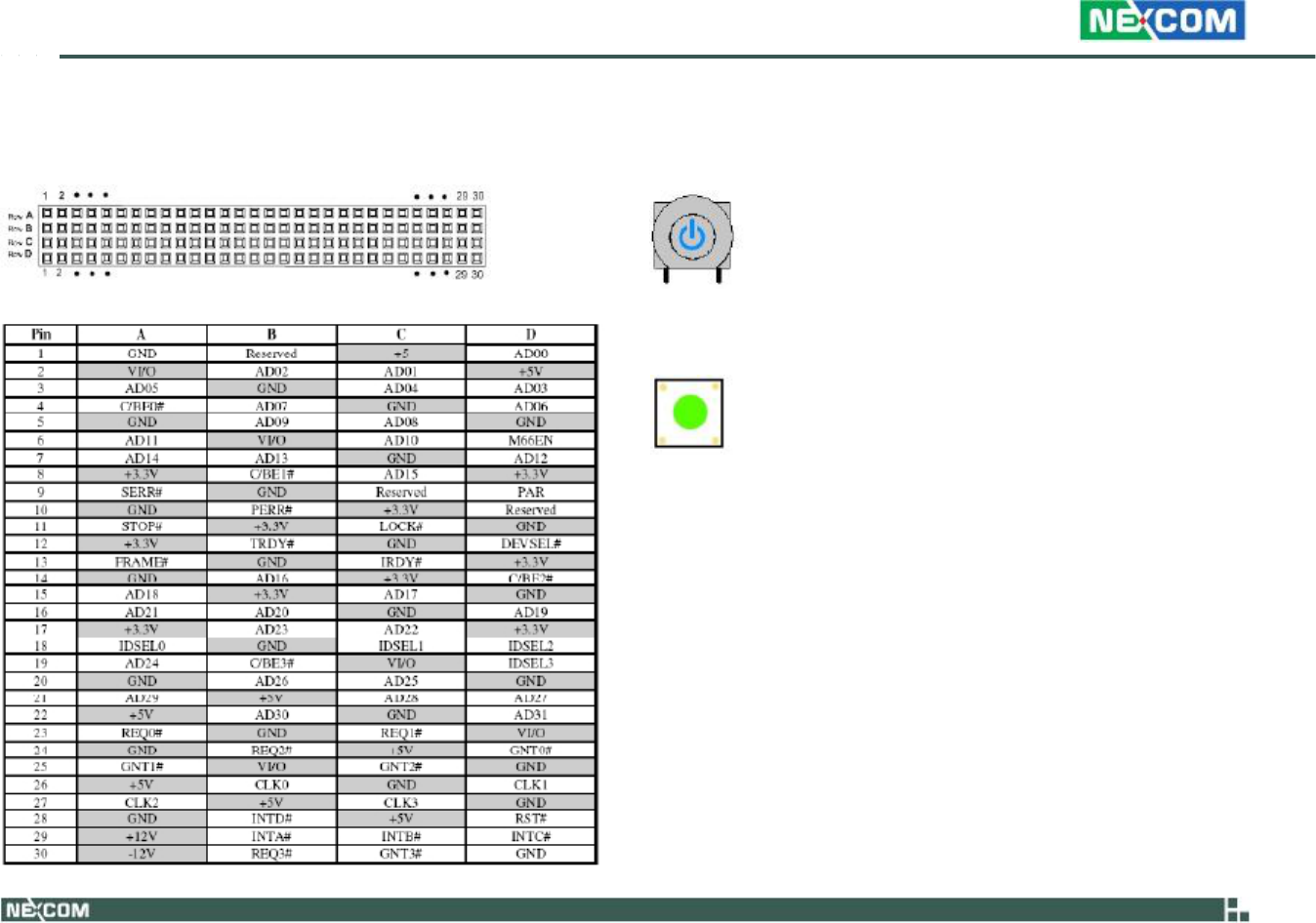
Chapter
2:
Jumpers
and
Connectors
PCI-104
Connector
Connector
location:
CN16
Connector
Pin
Definition
Copyright
©
2009
NEXCOM
International
Co.,
Ltd.
All
Rights
Reserved.
31
Power
Button
Connector
location:
SW1
Reset
Button
Connector
location:
SW2
VTC
6110
User
Manual

Chapter
2:
Jumpers
and
Connectors
MCU
COM
Port
Connector
location:
JP3
Connector
Pin
Definition
Copyright
©
2009
NEXCOM
International
Co.,
Ltd.
All
Rights
Reserved.
32
ACC_ON
LED
Connector
location:
JP7
1
Connector
Pin
Definition
VTC
6110
User
Manual
Pin
Function
Description
1
TX
2
RX
3
GND
Pin
Function
Description
1
+3.3V
LED
2
GND
Chapter
2:
Jumpers
and
Connectors
Temp
Sensor
Connector
location:
JP8
DC
Power
Input
Connector
Connector
location:
CN1
1
Connector
Pin
Definition
Connector
Pin
Definition
Copyright
©
2009
NEXCOM
International
Co.,
Ltd.
All
Rights
Reserved.
33
VTC
6110
User
Manual
Pin
Function
Description
1
GND
2
VIN
(6V~36V)
3
IGNITION
Pin
Function
Description
1
SENSOR+
2
GND

Chapter
2:
Jumpers
and
Connectors
Power
On
and
IDE
Active
LED
Connector
location:
LED1
T1
B1
Connector
Pin
Definition
Copyright
©
2009
NEXCOM
International
Co.,
Ltd.
All
Rights
Reserved.
34
GPIO
and
UMTS
LEDs
Connector
location:
LED2
T2
B2
LED
I/O
Port
Address
and
Data
VTC
6110
User
Manual
LED
Function
Description
T2
I/O
PORT
Address:
0EE0;
Bit0:
1
(Light),
0
(Dark)
B2
UMTS
STATUS
LED
Function
Description
T1
POWER
LED
B1
HD
LED
Chapter
2:
Jumpers
and
Connectors
Serial
ATA
Connector
location:
CN6
Serial
ATA
Power
Input
Connector
location:
J10
7
1
4
1
Connector
Pin
Definition
Copyright
©
2009
NEXCOM
International
Co.,
Ltd.
All
Rights
Reserved.
35
Connector
Pin
Definition
VTC
6110
User
Manual
Pin
Definition
Pin
Definition
1
GND
2
SATA_TXP0
-
3
SATA_TXN0
4
GND
5
SATA_RXN0
6
SATA_RXP0
7
GND
Pin
Definition
Pin
Definition
1
+V12S
2
GND
3
GND
4
+V5S
Chapter
2:
Jumpers
and
Connectors
Mini-PCIe
Socket
(for
3.5G
module)
PCIe
Interface
Connector
location:
CN10
Mini-PCIe
Socket
(for
WLAN
module)
USB
+
PCIe
Interface
Connector
location:
CN13
2
1
52
51
2
1
52
51
Connector
Pin
Definition
Copyright
©
2009
NEXCOM
International
Co.,
Ltd.
All
Rights
Reserved.
36
Connector
Pin
Definition
VTC
6110
User
Manual
Pin
Definition
Pin
Definition
Pin
Definition
Pin
Definition
1
MIC
+
2
+V3.3S
27
GND
28
NC
3
MIC
-
4
GND
29
GND
30
NC
5
SPK
+
6
NC
31
NC
32
NC
7
GND
8
USIM
PWR
33
RESET
34
GND
9
GND
10
USIM
DATa
35
GND
36
USB_D-
11
VCC_
MSM26_
DIG
12
USIM
CLK
37
GND
38
USB_D+
13
NC
14
USIM
RST
39
+V3.3S
40
GND
15
GND
16
NC
41
+V3.3S
42
LED_
WWAN#
17
NC
18
GND
43
GND
44
NC
19
NC
20
W_DIS-
ABLE#
45
NC
46
NC
21
GND
22
NC
47
NC
48
NC
23
NC
24
NC
49
NC
50
GND
25
NC
26
GND
51
NC
52
+V3.3S
Pin
Definition
Pin
Definition
Pin
Definition
Pin
Definition
1
WAKE#
2
+V3.3S
27
GND
28
+V1.5S
3
NC
4
GND
29
GND
30
SMB_CLK
5
NC
6
+V1.5S
31
PETn0
32
SMB_DATA
7
CLKREQ#
8
NC
33
PETp0
34
GND
9
GND
10
NC
35
GND
36
USB_D-
11
REFCLK-
12
NC
37
NC
38
USB_D+
13
REFCLK+
14
NC
39
NC
40
GND
15
GND
16
NC
41
NC
42
LED_
WWAN#
17
NC
18
GND
43
NC
44
LED_
WLAN#
19
NC
20
DISABLE#
45
NC
46
LED_
WPAN#
21
GND
22
PERST#
47
NC
48
+V1.5S
23
PERn0
24
+3.3S
49
NC
50
GND
25
PERp0
26
GND
51
NC
52
+V3.3S

MH2
MH1
Chapter
2:
Jumpers
and
Connectors
SIM
Card
Connector
Connector
location:
CN4
Bluetooth
Connector
Connector
location:
J7
1
2
3
4
5
6
7
8
109
J7
Connector
Pin
Definition
Copyright
©
2009
NEXCOM
International
Co.,
Ltd.
All
Rights
Reserved.
37
VTC
6110
User
Manual
Pin
Definition
Pin
Definition
1
GND
2
USB_6P_L
3
USB_6N_L
4
NC
5
NC
6
BT_AUDIO_EN_R
7
NC
8
BT_3.3V
9
NC
10
GND
Pin
Definition
Pin
Definition
C1
POWER
VOLTAGE
C2
RESET
SIGNAL
C3
CLOCK
SIGNAL
C5
GND
C6
VPP:PROGRAM
VOLTAGE
C7
I/O
SW
Contact
present
switch
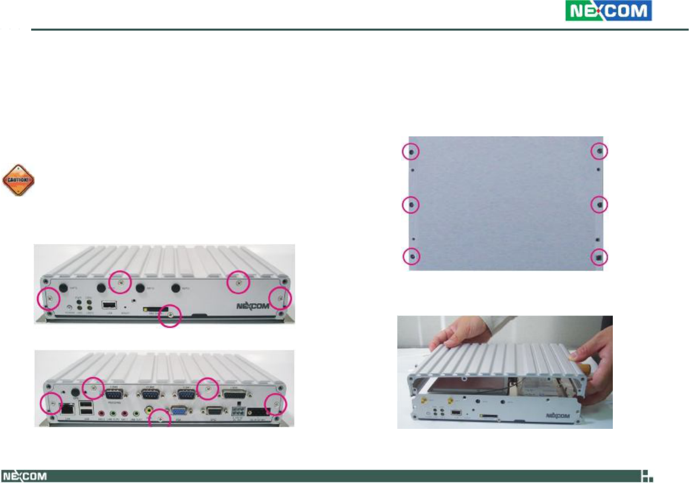
Chapter
3:
System
Setup
C
HAPTER
3:
S
YSTEM
S
ETUP
Removing
the
Chassis
Cover
Prior
to
removing
the
chassis
cover,
make
sure
the
unit’s
power
is
off
and
disconnected
from
the
power
sources
to
prevent
electric
shock
or
system
damage.
1.
The
screws
on
the
cover
are
used
to
secure
the
cover
to
the
chassis.
Remove
these
screws
and
put
them
in
a
safe
place
for
later
use.
Bottom
View
2.
Lift
the
cover
upward
then
remove
it
from
the
chassis.
Front
View
Rear
View
Copyright
©
2009
NEXCOM
International
Co.,
Ltd.
All
Rights
Reserved.
38
VTC
6110
User
Manual
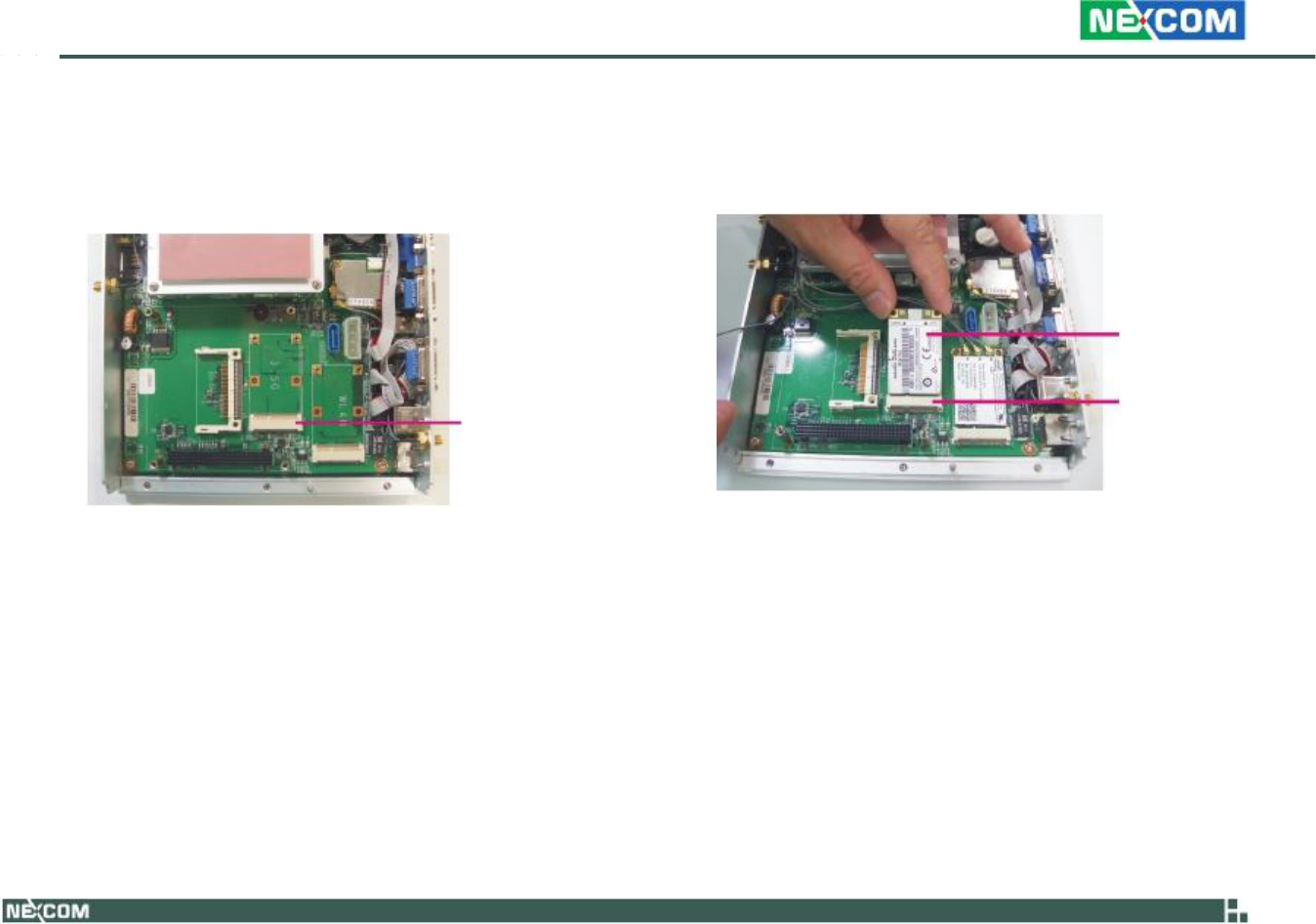
Chapter
3:
System
Setup
Installing
a
GPRS/UMTS/HSDPA
Module
1.
The
Mini
PCI
Express
slot
shown
below
is
used
to
install
a
3.5G
com-
munication
module
such
as
GPRS,
UMTS
or
HSDPA
module.
Mini
PCI
Express
slot
Copyright
©
2009
NEXCOM
International
Co.,
Ltd.
All
Rights
Reserved.
39
2.
Insert
the
module
into
the
Mini
PCI
Express
slot
at
a
45
degrees
angle
until
the
gold-plated
connector
on
the
edge
of
the
module
completely
disappears
inside
the
slot.
GPRS/UMTS/
HSDPA
module
Mini
PCI
Express
slot
VTC
6110
User
Manual
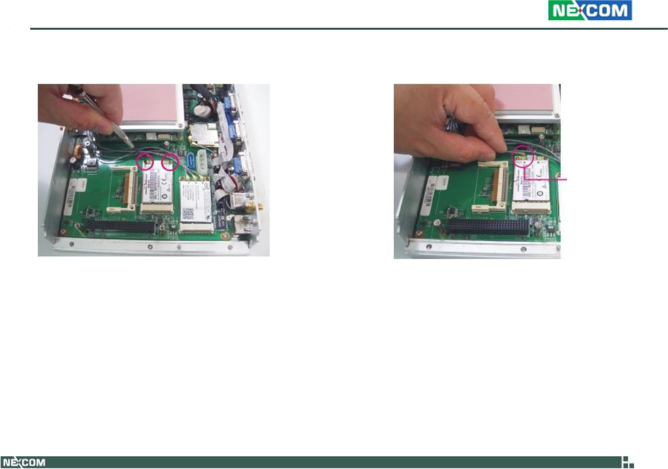
Chapter
3:
System
Setup
3.
Push
the
module
down
then
secure
it
with
mounting
screws.
4.
Attach
one
end
of
the
RF
cable
onto
the
module.
Attach
RF
cable
to
the
module
Copyright
©
2009
NEXCOM
International
Co.,
Ltd.
All
Rights
Reserved.
40
VTC
6110
User
Manual
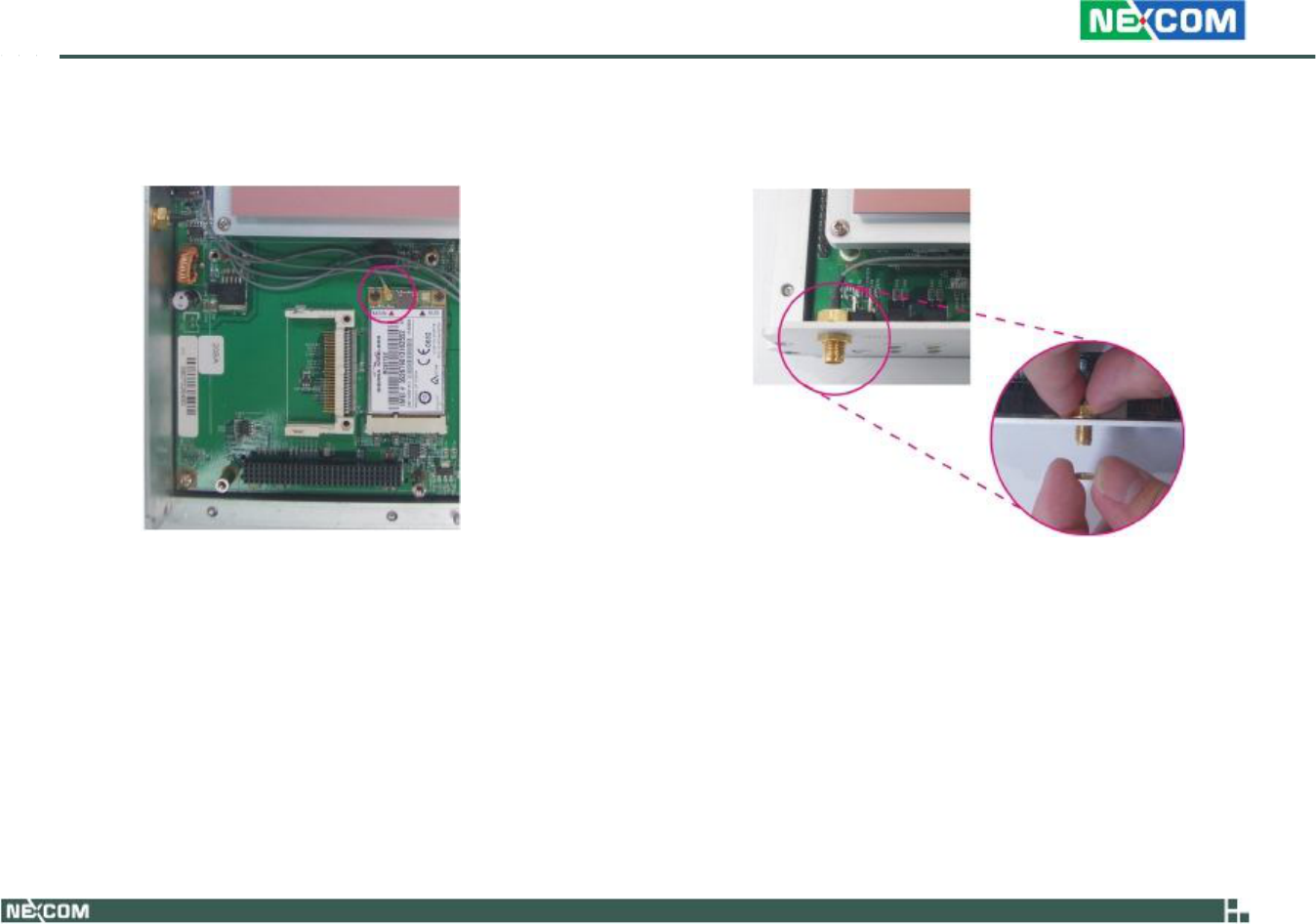
Chapter
3:
System
Setup
5.
The
photo
below
shows
one
end
of
the
RF
cable
properly
attached
onto
the
module.
Copyright
©
2009
NEXCOM
International
Co.,
Ltd.
All
Rights
Reserved.
41
6.
Mount
the
other
end
of
the
cable
to
the
antenna
mounting
hole
lo-
cated
at
the
front
panel
of
the
chassis.
RF
cable
mounted
at
the
front
panel
VTC
6110
User
Manual
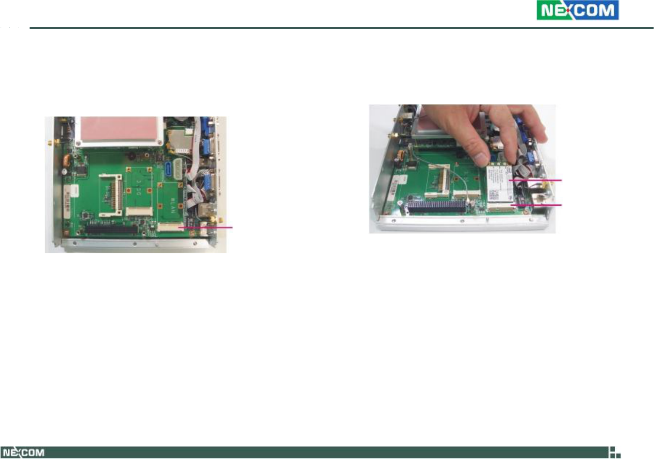
Chapter
3:
System
Setup
Installing
a
Wireless
LAN
Module
1.
The
Mini
PCI
Express
slot
shown
below
is
used
to
install
a
wireless
LAN
module.
2.
Insert
the
wireless
LAN
module
into
the
Mini
PCI
Express
slot
at
a
45
degrees
angle
until
the
gold-plated
connector
on
the
edge
of
the
mod-
ule
completely
disappears
inside
the
slot.
Wireless
LAN
module
Mini
PCI
Express
slot
Mini
PCI
Express
slot
Copyright
©
2009
NEXCOM
International
Co.,
Ltd.
All
Rights
Reserved.
42
VTC
6110
User
Manual
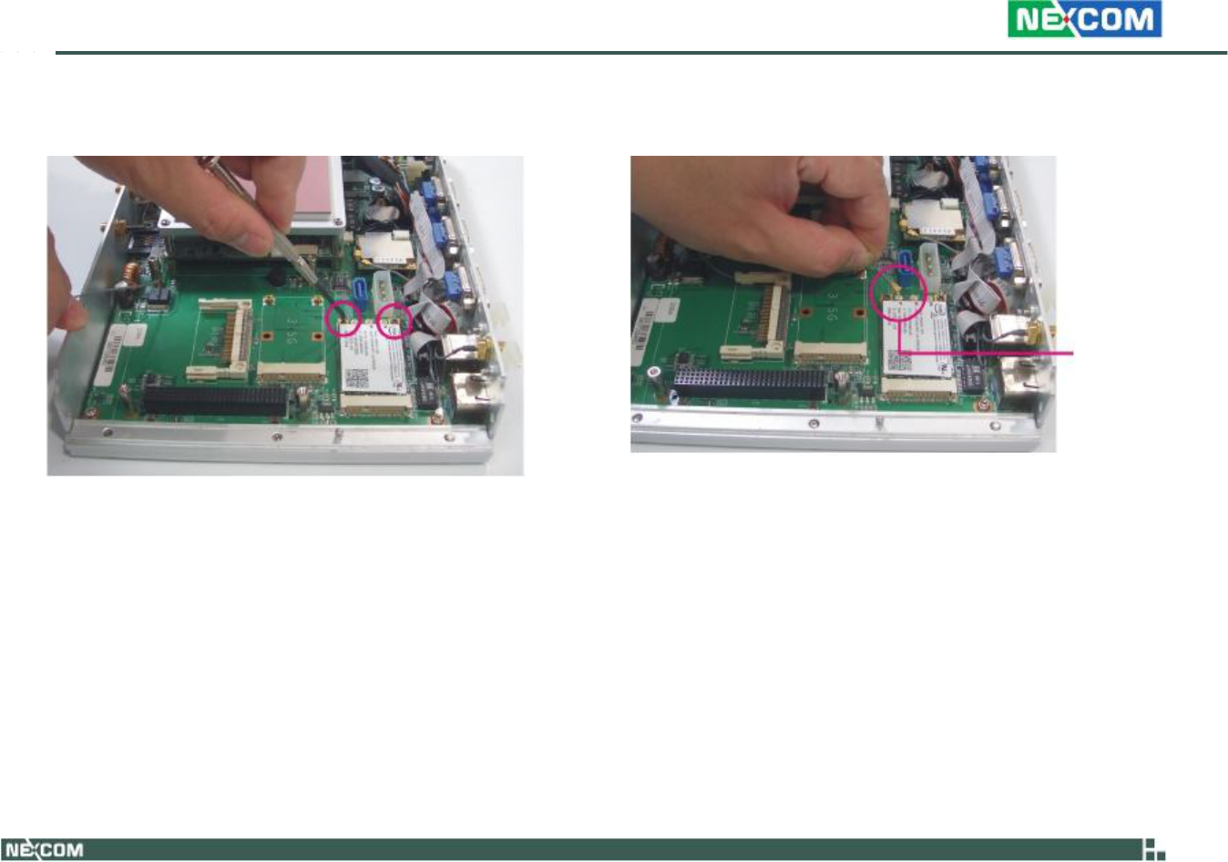
Chapter
3:
System
Setup
3.
Push
the
module
down
then
secure
it
with
mounting
screws.
4.
Attach
one
end
of
the
RF
cable
onto
the
module.
Attach
RF
cable
to
the
module
Copyright
©
2009
NEXCOM
International
Co.,
Ltd.
All
Rights
Reserved.
43
VTC
6110
User
Manual

Chapter
3:
System
Setup
5.
The
photo
below
shows
one
end
of
the
RF
cable
properly
attached
onto
the
module.
Copyright
©
2009
NEXCOM
International
Co.,
Ltd.
All
Rights
Reserved.
44
6.
Mount
the
other
end
of
the
cable
to
the
antenna
mounting
hole
lo-
cated
at
the
front
panel
of
the
chassis.
RF
cable
mounted
at
the
front
panel
VTC
6110
User
Manual
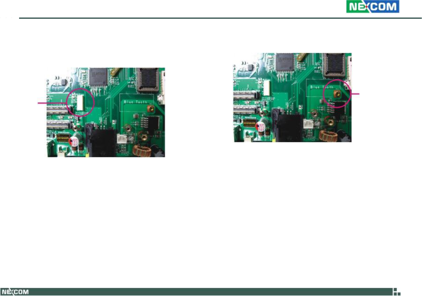
Chapter
3:
System
Setup
Installing
a
Bluetooth
Module
1.
The
USB
header
shown
below
is
used
to
install
a
Bluetooth
module.
USB
header
Copyright
©
2009
NEXCOM
International
Co.,
Ltd.
All
Rights
Reserved.
45
2.
Install
the
provided
mounting
stud
as
shown
in
the
illustration
below.
Mounting
stud
VTC
6110
User
Manual
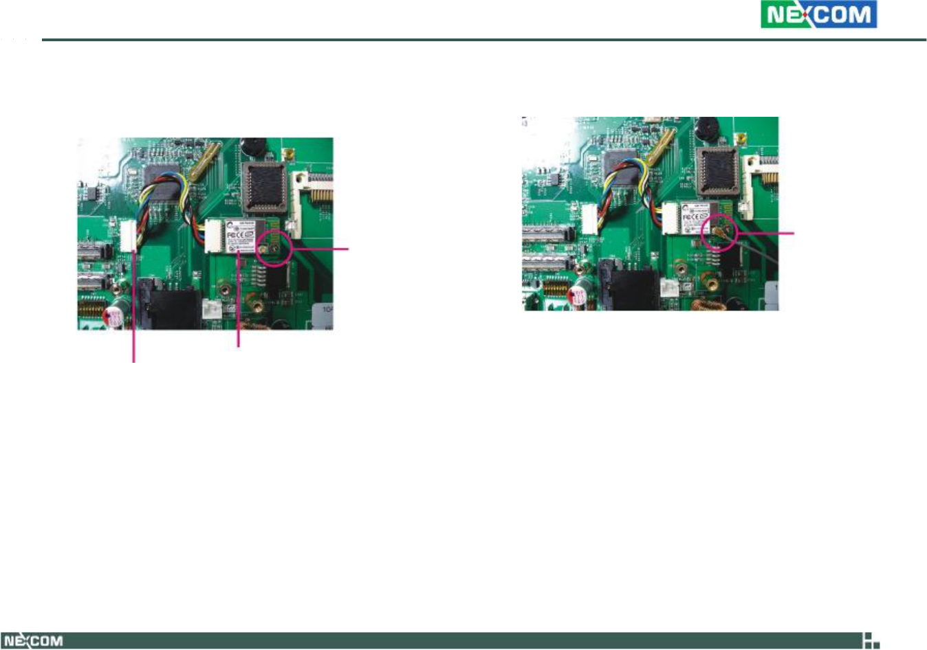
Chapter
3:
System
Setup
3.
Insert
the
Bluetooth
module’s
cable
connector
into
the
USB
header.
Push
the
module
down
then
secure
it
with
a
mounting
screw.
Mounting
screw
Bluetooth
module
Cable
connector
Copyright
©
2009
NEXCOM
International
Co.,
Ltd.
All
Rights
Reserved.
46
4.
Attach
one
end
of
the
RF
cable
onto
the
module.
Attach
RF
cable
to
the
module
5.
Mount
the
other
end
of
the
cable
to
the
Bluetooth
mounting
hole
located
at
the
front
panel
of
the
chassis.
VTC
6110
User
Manual
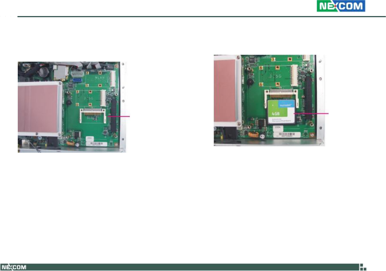
Chapter
3:
System
Setup
Installing
a
CompactFlash
Card
1.
Locate
for
the
CompactFlash
socket
on
the
board.
CompactFlash
socket
Copyright
©
2009
NEXCOM
International
Co.,
Ltd.
All
Rights
Reserved.
47
2.
With
the
CompactFlash
card’s
label
facing
up,
position
the
card
to
the
socket.
CompactFlash
card
VTC
6110
User
Manual
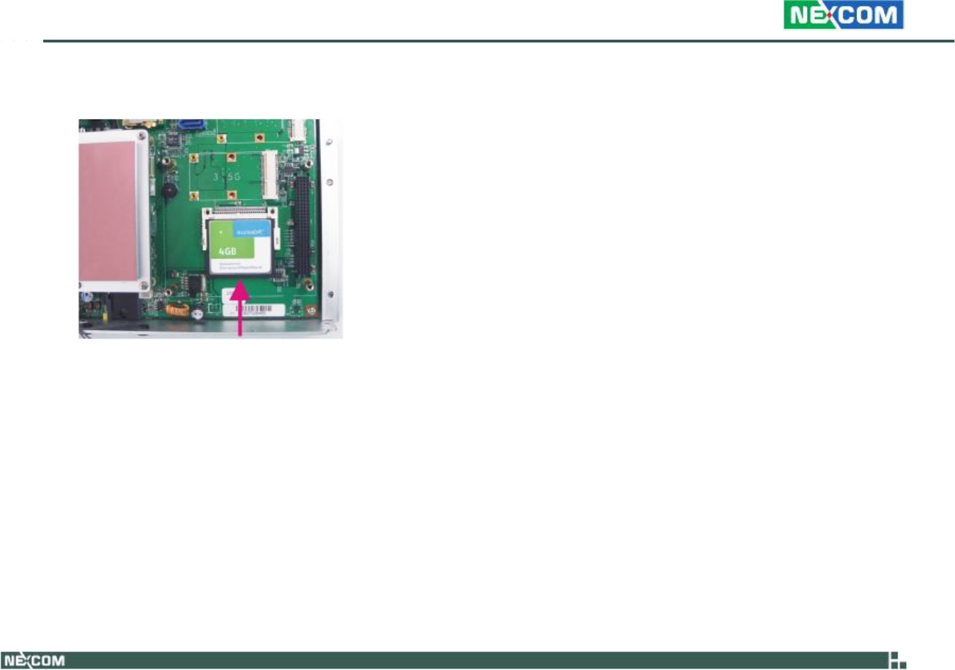
Chapter
3:
System
Setup
3.
Insert
the
card
until
it
is
completely
seated
in
the
socket.
Copyright
©
2009
NEXCOM
International
Co.,
Ltd.
All
Rights
Reserved.
48
VTC
6110
User
Manual
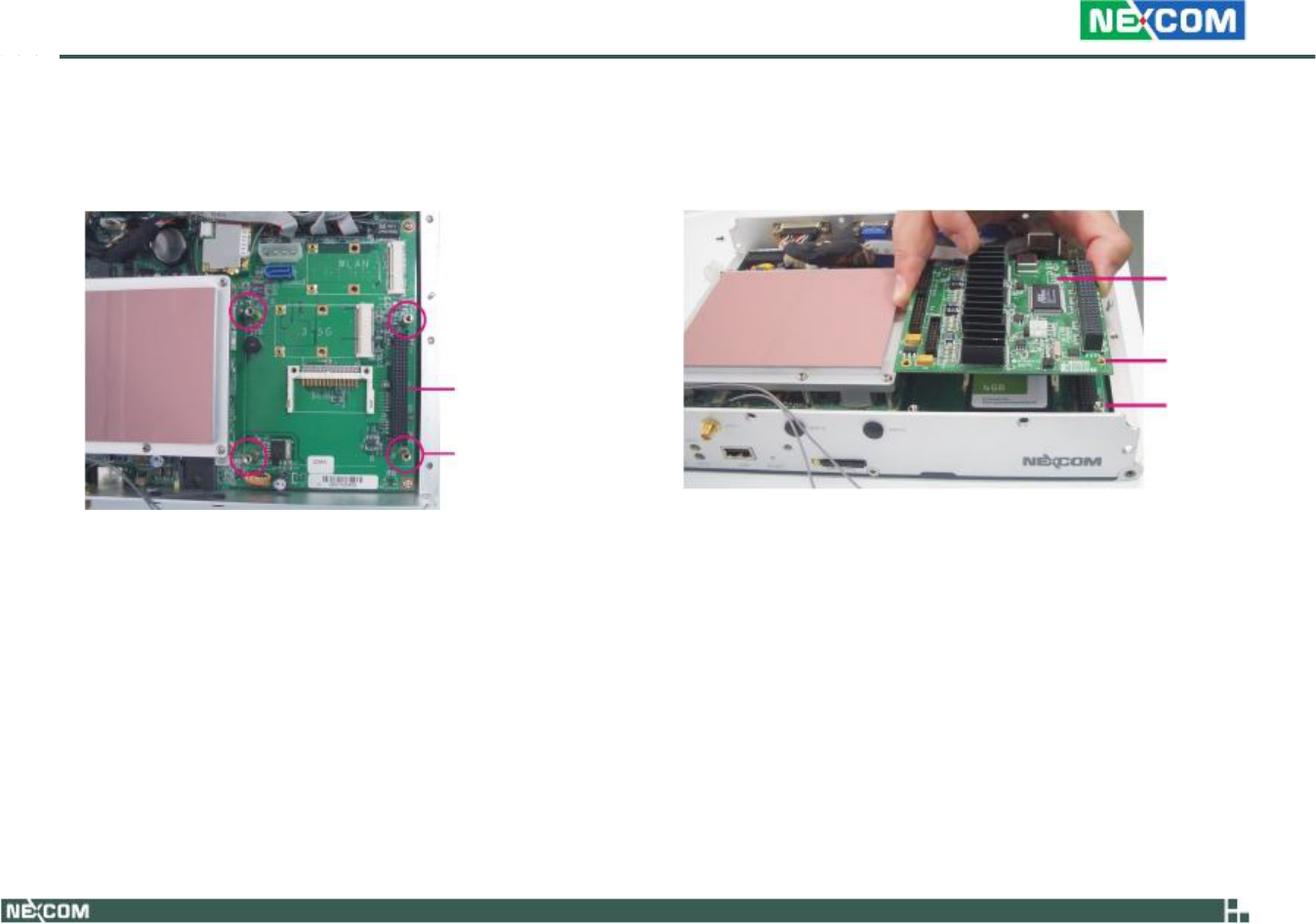
Chapter
3:
System
Setup
Installing
the
PCI-104
Module
1.
Locate
for
the
PCI-104
slot
on
the
board.
PCI-104
slot
Mounting
stud
Copyright
©
2009
NEXCOM
International
Co.,
Ltd.
All
Rights
Reserved.
49
2.
Position
the
PCI-104
module
above
the
slot
then
press
it
down
firmly
until
it
is
completely
seated
in
the
slot.
This
will
at
the
same
time
align
the
module’s
mounting
holes
to
the
mounting
studs
on
the
board.
PCI-104
module
Mounting
hole
Mounting
stud
VTC
6110
User
Manual
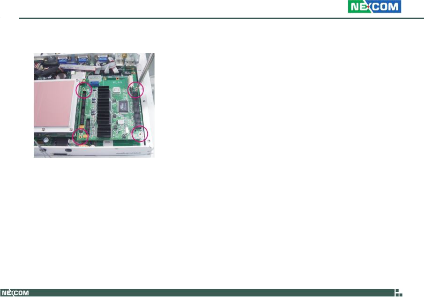
Chapter
3:
System
Setup
3.
Secure
the
module
with
mounting
screws.
Copyright
©
2009
NEXCOM
International
Co.,
Ltd.
All
Rights
Reserved.
50
VTC
6110
User
Manual
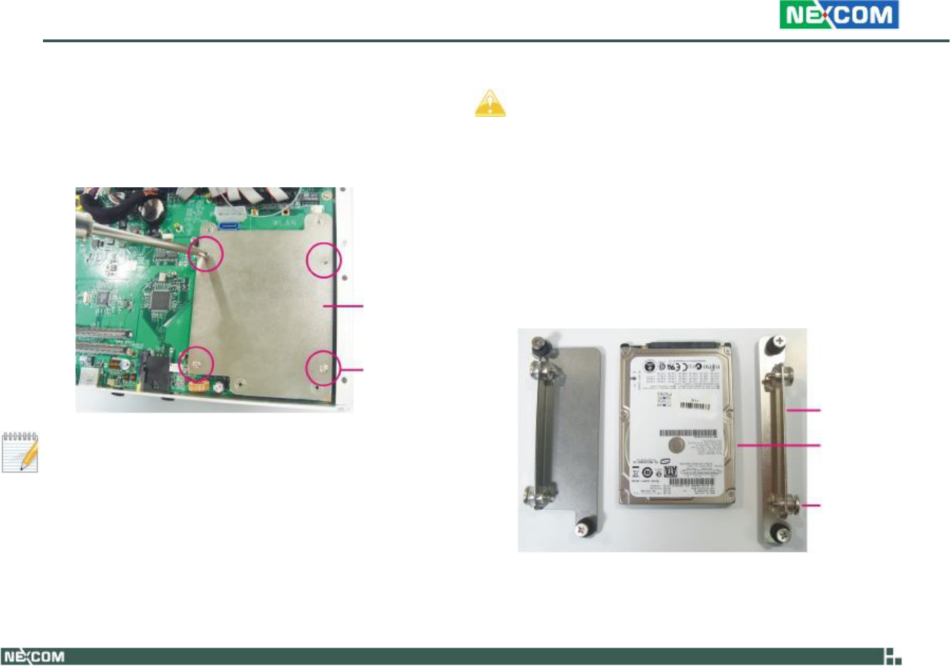
Chapter
3:
System
Setup
Installing
a
SATA
Hard
Drive
1.
The
metal
bracket
is
used
to
hold
a
SATA
hard
drive.
First,
remove
the
screws
that
secure
the
metal
bracket
to
the
board
then
remove
the
bracket.
Metal
bracket
·
During
Windows
XP
OS
installation,
press
“F6”
to
select
and
install
the
SATA
driver.
·
If
you
intend
to
install
a
Windows
XP
SP2
or
earlier
version,
you
must
first
set
the
“USB
2.0
Controller”
field
(in
the
BIOS)
to
Disabled.
·
By
default,
the
“Legacy
USB
Support”
field
(in
the
BIOS)
is
Disabled.
If
you
are
using
a
USB
device
to
install
the
Windows
operating
system,
you
must
first
set
this
field
to
Enabled.
Set
this
field
back
to
Disabled
after
you
have
finished
the
installation.
2.
Position
the
HDD
brackets
on
each
side
of
the
SATA
drive.
Align
the
mounting
holes
that
are
on
the
sides
of
the
SATA
drive
with
the
HDD
brackets’
mounting
screws.
Mounting
screws
HDD
bracket
If
you
intend
to
install
a
CompactFlash
card
or
a
Mini
PCI
Express
module,
please
install
these
devices
first
before
proceeding
to
the
next
step.
Refer
to
their
respective
sections
in
this
chapter
for
in-
structions
on
installing
a
CF
card
or
a
Mini
PCI
Express
module.
Copyright
©
2009
NEXCOM
International
Co.,
Ltd.
All
Rights
Reserved.
51
SATA
drive
Mounting
screws
VTC
6110
User
Manual
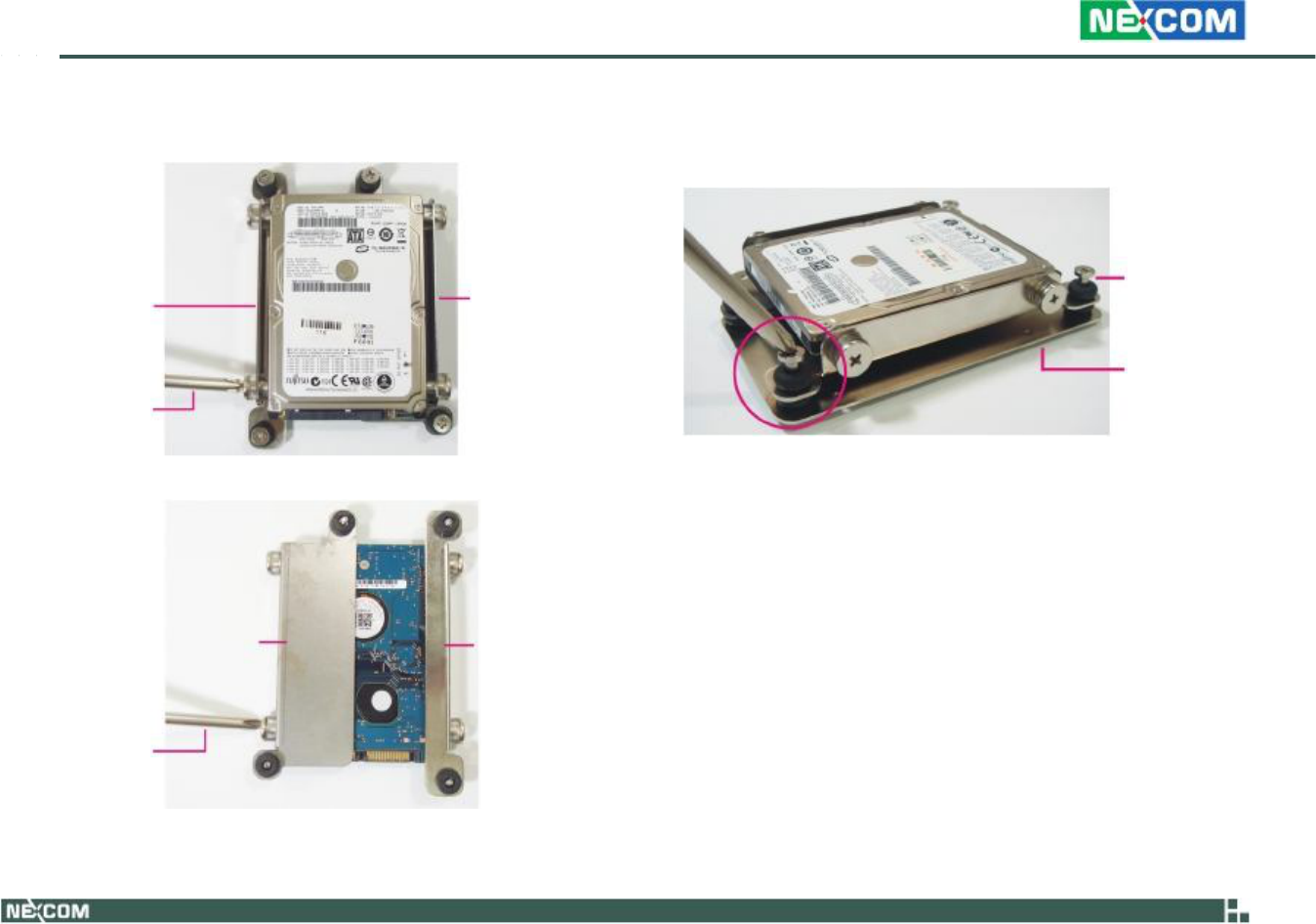
Chapter
3:
System
Setup
3.
Tighten
the
mounting
screws
to
secure
the
HDD
brackets
in
place.
4.
Now
place
the
SATA
drive
on
the
metal
bracket
then
tighten
the
head
bolt
screws
to
secure
the
drive
on
the
metal
bracket.
Head
bolt
screw
HDD
bracket
HDD
bracket
Metal
bracket
Screwdriver
Top
View
HDD
bracket
HDD
bracket
Screwdriver
Bottom
View
Copyright
©
2009
NEXCOM
International
Co.,
Ltd.
All
Rights
Reserved.
52
VTC
6110
User
Manual
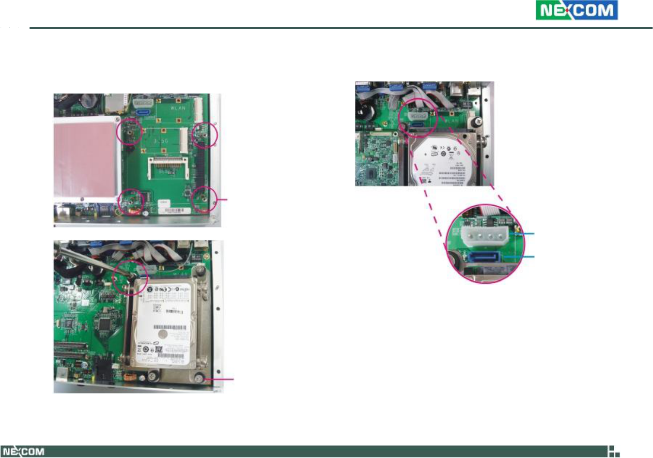
Chapter
3:
System
Setup
5.
Align
the
head
bolt
screws
with
the
mounting
studs
on
the
board.
6.
Locate
for
the
SATA
connector
and
the
power
connector.
on
the
board.
Tighten
the
head
bolt
screws
to
secure
the
drive
to
the
chassis.
Mounting
stud
Power
connector
SATA
connector
Head
bolt
screw
Copyright
©
2009
NEXCOM
International
Co.,
Ltd.
All
Rights
Reserved.
53
VTC
6110
User
Manual
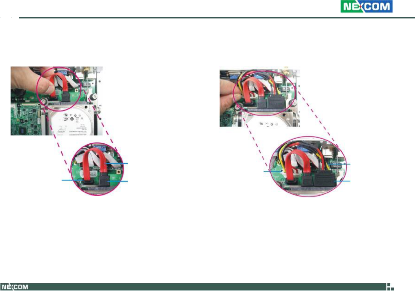
Chapter
3:
System
Setup
7.
Connect
one
end
of
the
SATA
data
cable
to
the
SATA
connector
that
is
on
the
board
then
connect
the
other
end
of
the
cable
to
the
SATA
con-
nector
at
the
rear
of
the
SATA
drive.
8.
Connect
one
end
of
the
SATA
power
cable
to
the
SATA
power
connec-
tor
that
is
on
the
board
then
connect
the
other
end
of
the
cable
to
the
SATA
power
connector
at
the
rear
of
the
SATA
drive.
Cable
connected
to
the
SATA
connector
on
the
board
SATA
data
cable
Cable
connected
to
the
SATA
drive
Cable
connected
to
the
SATA
power
connector
on
the
board
SATA
power
cable
Cable
connected
to
the
SATA
drive
Copyright
©
2009
NEXCOM
International
Co.,
Ltd.
All
Rights
Reserved.
54
VTC
6110
User
Manual

Chapter
3:
System
Setup
Installing
the
SODIMM
1.
Remove
the
heatspreader’s
mounting
screws.
Heatspreader
Copyright
©
2009
NEXCOM
International
Co.,
Ltd.
All
Rights
Reserved.
55
2.
Insert
the
module
into
the
socket
at
an
approximately
30
degrees
angle.
Apply
firm
even
pressure
to
each
end
of
the
module
until
it
slips
into
the
socket.
The
gold-plated
connector
on
the
edge
of
the
module
will
almost
completely
disappear
inside
the
socket.
SODIMM
socket
SODIMM
VTC
6110
User
Manual

Chapter
3:
System
Setup
3.
Push
the
module
down
until
the
clips
on
both
sides
of
the
socket
lock
into
position.
You
will
hear
a
distinctive
“click”,
indicating
the
module
is
correctly
locked
into
position.
Clip
Copyright
©
2009
NEXCOM
International
Co.,
Ltd.
All
Rights
Reserved.
56
VTC
6110
User
Manual
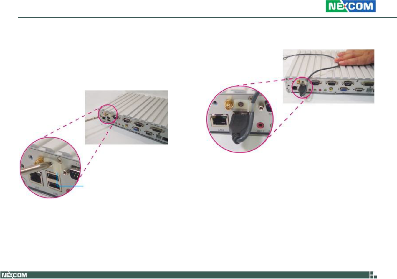
Chapter
3:
System
Setup
Installing
the
USB
Cable
Holder
The
USB
cable
holder
is
used
to
stabilize
the
USB
cable
so
as
to
prevent
it
from
getting
loose
when
accidentally
pulled
or
moved.
1.
Attach
the
cable
holder
to
the
mounting
hole
by
using
the
provided
screw.
Cable
holder
Copyright
©
2009
NEXCOM
International
Co.,
Ltd.
All
Rights
Reserved.
57
2.
Hook
the
cable
to
the
holder
as
shown
in
the
photo
below.
VTC
6110
User
Manual
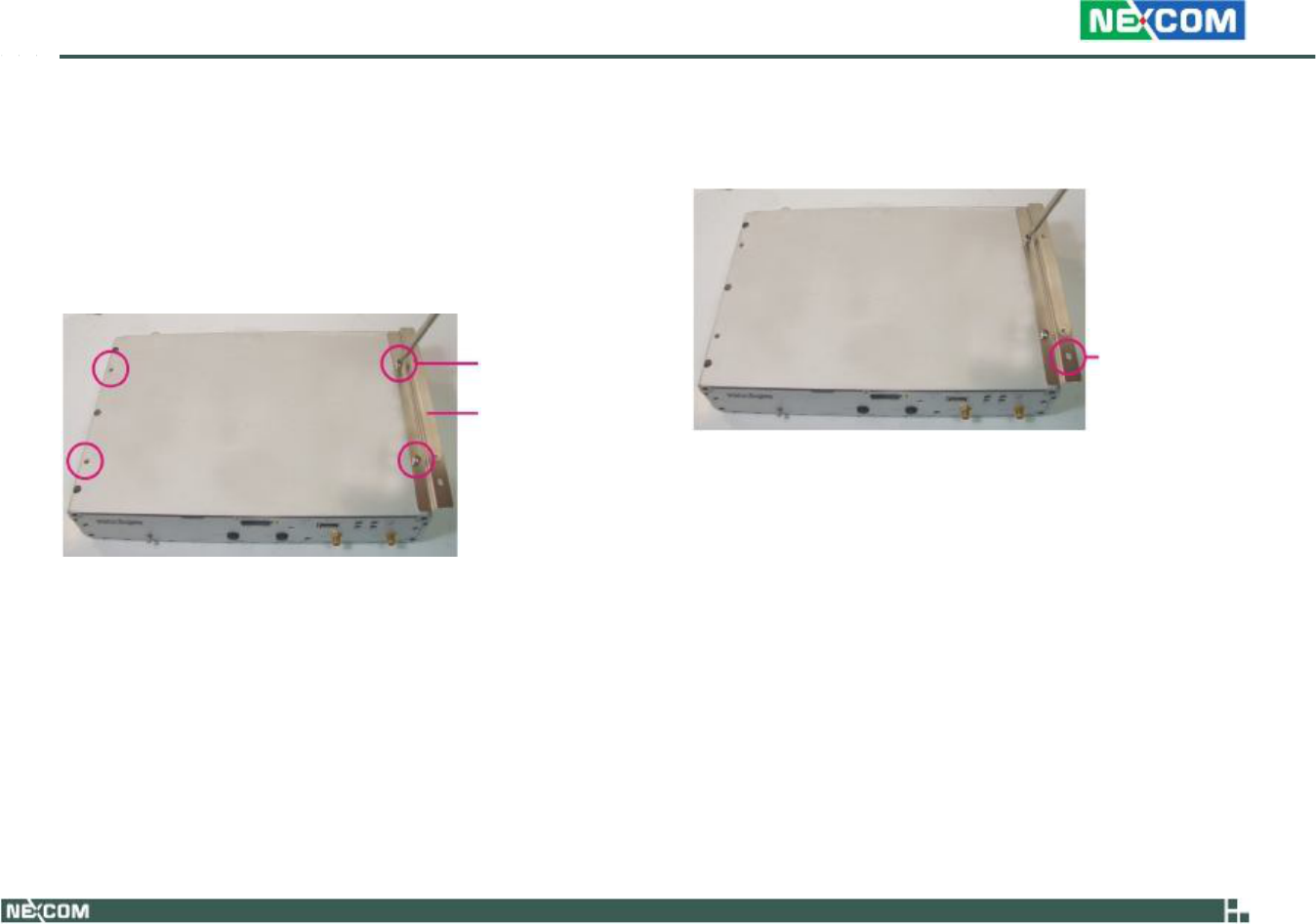
Chapter
3:
System
Setup
Rackmount
Brackets
The
rackmount
brackets
provide
a
convenient
and
economical
way
of
mounting
the
system
on
the
wall.
1.
The
mounting
holes
are
located
at
the
bottom
of
the
system.
Secure
the
brackets
on
each
side
of
the
system
using
the
provided
mounting
screws.
Secure
the
bracket
to
the
system
Rackmount
bracket
Copyright
©
2009
NEXCOM
International
Co.,
Ltd.
All
Rights
Reserved.
58
2.
Now
mount
the
system
on
the
wall
by
fastening
screws
through
the
bracket’s
mounting
holes.
Fasten
screws
to
mount
the
system
to
the
wall
VTC
6110
User
Manual
Appendix
A:
I/O
Address
Function
A
PPENDIX
A:
I/O
A
DDRESS
F
UNCTION
GPIO
LED
/
UMTS
LED
/
Ignition
Status
I/O
port
:
0EE0H
Capacity
of
NEXCOM
battery
(8
bits)
I/O
port
:
0EE1H
Voltage
of
NEXCOM
battery
(8
bits)
I/O
port
:
0EE2H
Copyright
©
2009
NEXCOM
International
Co.,
Ltd.
All
Rights
Reserved.
59
VTC
6110
User
Manual
Bit
Function
Description
Bit
0
GPIO
LED
0:
OFF
(default)
1:
ON
Bit
1
UMTS
LED
0:
LED
for
WLAN
(default)
1:
LED
for
3.5G
and
WLAN
Bit
2
Ignition
(read
only)
0:
OFF
1:
ON
Bit
3
Status
of
Vehicle
Battery
0:
Vehicle
Battery
is
OK
1:
Vehicle
Battery
is
Low
Voltage
Bit0
Bit1
Bit2
Bit3
Bit4
Bit5
Bit6
Bit7
Description
8
bits
data
(Bit
7
is
highest
bit
of
data)
Bit0
Bit1
Bit2
Bit3
Bit4
Bit5
Bit6
Bit7
Description
8
bits
data
(Bit
7
is
highest
bit
of
data)

Appendix
A:
I/O
Address
Function
Status
of
NEXCOM
battery
(8
bits)
I/O
port
:
0EE3H
GPIO
I/O
port
:
0EE4H
Copyright
©
2009
NEXCOM
International
Co.,
Ltd.
All
Rights
Reserved.
60
VTC
6110
User
Manual
Bit
Function
Description
Bit
0
Status
for
G
sensor
detection
0:
Normal
1:
Abnormal
(X-axis
or
Y-axis
degree
is
about
90
or
-90)
Bit
1
Power
mode
0:
24V
system
1:
12V
system
Bit
2
Fan
mode
0:
Auto
1:
Always
on
Bit
3
Status
of
Smart
battery
0:
No
discharging
1:
Discharging
Bit
4
Status
of
Fan
R
0:
Well
1:
Failed
Bit
5
Status
of
Fan
R
0:
Action
1:
Inaction
Bit
6
Status
of
Fan
L
0:
Well
1:
Failed
Bit
7
Status
of
Fan
L
0:
Action
1:
Inaction
Bit
Function
Description
Bit
0-3
GPO
1-4
Bit
4-7
GP
I
1-4
Appendix
A:
I/O
Address
Function
WDT
I/O
port
:
0EE5H
Onboard
Module
Disable/Enable
I/O
port
:
0EE6H
Bit
2,
1,
0:
Time
Setting
Auto
clear
WDT
timer
when
reading/writing
I/O
port
0EE5H.
Copyright
©
2009
NEXCOM
International
Co.,
Ltd.
All
Rights
Reserved.
61
VTC
6110
User
Manual
Bit
Function
Description
Bit
0
3.5G
module
0:
Disable
1:
Enable
(default)
Bit
1
WLAN
module
0:
Disable
1:
Enable
(default)
Bit
2
External
+12V
power
0:
Disable
1:
Enable
(default)
Bit
3
External
+5V
power
0:
Disable
1:
Enable
(default)
Bit
2~0
Time
(sec)
000
1
(default)
001
2
010
4
011
8
100
16
101
32
110
64
111
128
Bit
Function
Description
Bit
3
WDT
Disable/Enable
0:
Disable
(default)
1:
Enable

Appendix
B:
ICES200-L24
COM
Express
CPU
Module
A
PPENDIX
B:
ICES200-L24
COM
E
XPRESS
CPU
M
ODULE
Overview
ICES
200
is
a
Type
2
COM
Express
Module
that
features
Intel
®
945GME
and
ICH7M
chipset;
switch
supports
Intel
®
Core™
2
Duo
and
Intel
®
Core™
2
Duo
LV
processors
with
533/667
MHz
FSB.
One
DDR2
memory
socket
supports
up
to
2GB.
The
ICES
200
is
integrated
with
Intel
®
Graphics
Media
Accelerator
(GMA950)
and
expands
via
PCI
Express
Graphics
x16
lanes
to
the
carrier
board.
It
also
supports
other
display
interfaces
including
LFP
or
Dual
channel
LVDS.
The
high
performance
ICES
200
COM
Express
Module
supports
2
x
SATA,
8
x
USB
2.0
and
4
PCIe
x1
Lanes
through
the
carrier
board.
Key
Features
·
Intel
®
Socket
M
supports
Core™
2
Duo
/
Core™
2
Duo
LV
Processor
Family
·
Intel
®
945GME
Chipset
·
One
DDR2
SO-DIMM
socket
supports
un-buffered
non-ECC
DDR2
533/667
up
to
2GB
·
Supports
2
x
Serial
ATA
for
high
speed
drives,
8
x
USB
2.0
for
fast
pe-
ripherals
·
Type
2
COM
Express
Module
supports
up
to
21
Express
lanes,
32
bit
PCI
interface,
one
IDE
and
Gigabit
LAN
Copyright
©
2009
NEXCOM
International
Co.,
Ltd.
All
Rights
Reserved.
62
VTC
6110
User
Manual

Appendix
B:
ICES200-L24
COM
Express
CPU
Module
Specifications
CPU
Support
·
Supports
Intel
®
Socket
M,
Core™
2
Duo
Family
Processors
·
Supports
533/667MHz
FSB
CPU
Main
Memory
·
1
x
DDR2
SO-DIMM
socket
Chipset
·
Intel
®
945GME
·
ICH7M
I/O
Controller
Hub
BIOS
·
Award
System
BIOS
·
Plug
&
Play
support
·
8Mbit
Flash
ROM
Onboard
LAN
·
Realtek
PCI
Express
GbE
8111C-GR
·
Supports
PXE
LAN
boot
function
·
Supports
Wake
on
LAN
Display
·
Integrated
with
Intel
®
Graphics
Media
Accelerator
(GMA950)
or
expand
via
PCI
Express
Graphics
x16
lanes
/
Dual
SDVO
·
CRT
resolution
up
to
2048
x
1536
@
60Hz,
1600
x
1200
@
85Hz
·
One
PCI
Express
x16
Lane
down
to
the
carrier
board
·
Supports
LFP
(Local
Flat
Panel)
LVDS
interface
with
resolution
up
to
1366
x
768
·
Supports
Single
channel
for
18
bit
/
Dual
Channel
for
18
bit
Audio
·
HD
audio
interface
COM
Express
Connectors
·
AB
-
VGA
/
LVDS
/
8
x
USB
2.0
/
HD
Audio
/
2
x
SATA
/
LAN
/
GPIO
/
LPC
bus
/
1
x
PCIe
x4
/
1
x
PCIe
x1
/
5
x
PCIe
x1
/
SMBus
(I2C)
/
SPI
BIOS
·
CD
-
PCIe
x16
/
IDE
/
PCI
System
Monitor
·
Derived
from
HW
monitor
·
Monitors
4
voltages,
2
temperatures
and
1
fan
speed
·
4
voltages
(For
+3.3
V,
+5
V,
+12
V,
Vcore)
·
2
temperatures
(CPU
and
one
external
Temperature
Sensor)
Power
Requirements
·
+
12
V,
+
5
VSB,
+
3.3
V
RTC
Copyright
©
2009
NEXCOM
International
Co.,
Ltd.
All
Rights
Reserved.
63
VTC
6110
User
Manual

Appendix B: ICES200-L24 COM Express CPU Module
Dimensions
· COM Express Basic Module Type 2
· 95mm x 125mm
Copyright
©
2009
NEXCOM
International
Co.,
Ltd.
All
Rights
Reserved.
64
VTC
6110
User
Manual
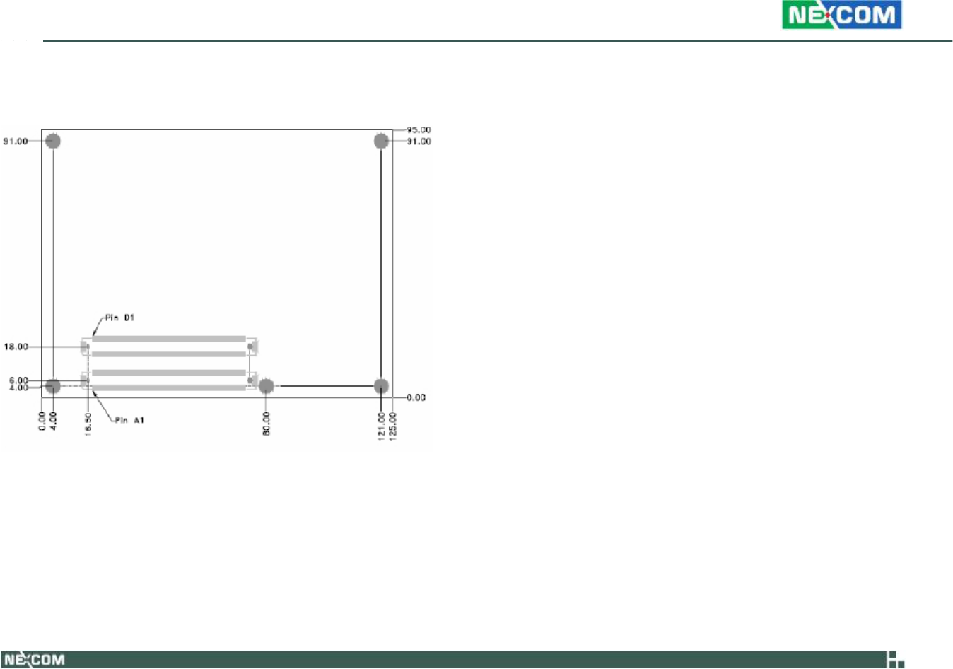
Appendix B: ICES200-L24 COM Express CPU Module
Mechanical
Dimensions
Copyright
©
2009
NEXCOM
International
Co.,
Ltd.
All
Rights
Reserved.
65
VTC
6110
User
Manual
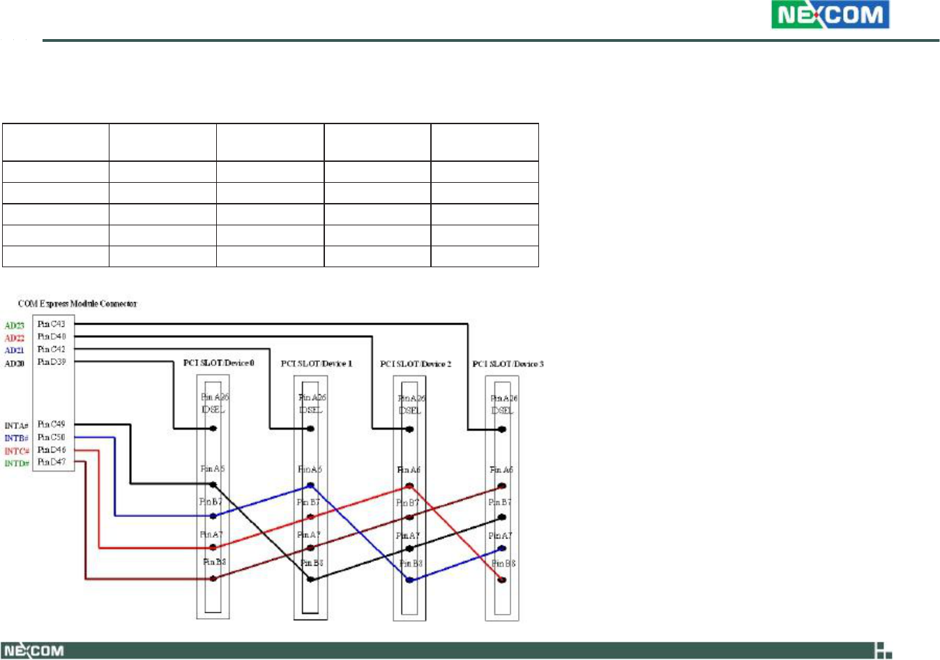
Appendix B: ICES200-L24 COM Express CPU Module
PCI
Routing
COM
Express
Module
Connector
Copyright
©
2009
NEXCOM
International
Co.,
Ltd.
All
Rights
Reserved.
66
VTC
6110
User
Manual
Slot
/
Device
Signal
Slot
/
Device
0
Slot
/
Device
1
Slot
/
Device
2
Slot
/
Device
3
IDSEL AD20 AD21 AD22 AD23
INTA# IRQA IRQB IRQC IRQD
INTB# IRQB IRQC IRQD IRQA
INTC# IRQC IRQD IRQA IRQB
INTD# IRQD IRQA IRQB IRQC

B1
B2
B3
B4
B5
B6
B7
B8
B
9
B10
B11
B12
B13
B14
B15
B16
B17
B18
B19
B20
B21
B22
B23
B24
B25
B26
B27
B28
B29
B30
B31
B32
B33
B34
B35
B36
B37
B38
B39
B40
B41
B42
B43
B44
B45
B46
B47
B48
B49
B50
B51
B52
B53
B54
B55
B56
B57
B58
B59
B60
B61
B62
B63
B64
B65
B66
B67
B68
B69
B70
B71
B72
B73
B74
B75
B76
B77
B78
B79
B80
B81
B82
B83
B84
B85
B86
B87
B88
B89
B90
B91
B92
B93
B94
B95
B96
B97
B98
B99
B100
B101
B102
B103
B104
B105
B106
B107
B108
B109
B110
B1
B2
B3
B4
B5
B6
B7
B8
B9
B10
B11
B12
B13
B14
B15
B16
B17
B18
B19
B20
B21
B22
B23
B24
B25
B26
B27
B28
B29
B30
B31
B32
B33
B34
B35
B36
B37
B38
B39
B40
B41
B42
B43
B44
B45
B46
B47
B48
B49
B50
B51
B52
B53
B54
B55
B56
B57
B58
B59
B60
B61
B62
B63
B64
B65
B66
B67
B68
B69
B70
B71
B72
B73
B74
B75
B76
B77
B78
B79
B80
B81
B82
B83
B84
B85
B86
B87
B88
B89
B90
B91
B92
B93
B94
B95
B96
B97
B98
B99
B100
B101
B102
B
103
B104
B105
B106
B107
B108
B109
B110
A1
A2
A3
A4
A5
A6
A7
A8
A9
A10
A11
A12
A13
A14
A15
A16
A17
A18
A19
A20
A21
A22
A23
A24
A25
A26
A27
A28
A29
A30
A31
A32
A33
A34
A35
A36
A37
A38
A39
A40
A41
A42
A43
A44
A45
A46
A47
A48
A49
A50
A51
A52
A53
A54
A55
A56
A57
A58
A59
A60
A61
A62
A63
A64
A65
A66
A67
A68
A69
A70
A71
A72
A73
A74
A75
A76
A77
A78
A79
A80
A81
A82
A83
A84
A85
A86
A87
A88
A89
A90
A91
A92
A93
A94
A95
A96
A97
A98
A99
A100
A101
A102
A103
A104
A105
A106
A107
A108
A109
A110
Appendix
B:
ICES200-L24
COM
Express
CPU
Module
Connectors
High
Speed
Board-to-Board
Connector:
COM
Express
Row
A
and
Row
B
Connector
size:
2
X
110
=
220
Pins
Connector
location:
J2
J1
C OM E xp re ss
Row
B
COM
Express
Connector
MH2
MH2
MH1
MH1
Row
A
Connector
Pin
Definition
Copyright
©
2009
NEXCOM
International
Co.,
Ltd.
All
Rights
Reserved.
67
VTC
6110
User
Manual
Row
A
Row
B
Row
A
Row
B
A13
GBE0_MDI0+
B13
SMB_CK
A68
PCIE_TX0+
B68
PCIE_RX0+
A14
GBE0_CTREF
B14
SMB_DAT
A69
PCIE_TX0-
B69
PCIE_RX0-
A15
SUS_S3#
B15
SMB_ALERT#
A70
GND
B70
GND
A16
SATA0_TX+
B16
SATA1_TX+
A71
LVDS_A0+
B71
LVDS_B0+
A17
SATA0_TX-
B17
SATA1_TX-
A72
LVDS_A0-
B72
LVDS_B0-
A18
SUS_S4#
B18
SUS_STAT#
A73
LVDS_A1+
B73
LVDS_B1+
A19
SATA0_RX+
B19
SATA1_RX+
A74
LVDS_A1+
B74
LVDS_B1-
A20
SATA0_RX-
B20
SATA1_RX-
A75
LVDS_A2+
B75
LVDS_B2+
A21
GND
B21
GND
A76
LVDS_A2+
B76
LVDS_B2-
A22
NC
B22
NC
A77
LVDS_VDD_EN
B77
LVDS_B3+
A23
NC
B23
NC
A78
LVDS_A3+
B78
LVDS_B3-
A24
SUS_S5#
B24
PWR_OK
A79
LVDS_A3+
B79
LVDS_BKLT_EN
A25
NC
B25
NC
A80
GND
B80
GND
A26
NC
B26
NC
A81
LVDS_A_CK+
B81
LVDS_B_CK+
A27
BATLOW#
B27
NC
A82
LVDS_A_CK-
B82
LVDS_B_CK-
A28
ATA_ACT#
B28
AC_SDIN2
A83
LVDS_I2C_CK
B83
LVDS_BKLT_
CTRL
A29
AC_SYNC
B29
AC_SDIN1
A84
LVDS_I2C_DAT
B84
VCC_5V_SBY
A30
AC_RST#
B30
AC_SDIN0
A85
GPI3
B85
VCC_5V_SBY
A31
GND
B31
GND
A86
KBD_RST#
B86
VCC_5V_SBY
A32
AC_BITCLK
B32
SPKR
A87
KBD_A20GATE
B87
VCC_5V_SBY
A33
AC_SDOUT
B33
I2C_CK
A88
PCIE0_CK_REF+
B88
RSVD
A34
BIOS_DISABLE#
B34
I2C_DAT
A89
PCIE0_CK_REF-
B89
VGA_RED
A35
THRMTRIP#
B35
THRM#
A90
GND
B90
GND
A36
USB6-
B36
USB7-
A91
RSVD
B91
VGA_GRN
A37
USB6+
B37
USB7+
A92
RSVD
B92
VGA_BLU
A38
USB_6_7_OC#
B38
USB_4_5_OC#
A93
GPO0
B93
VGA_HSYNC
A39
USB4-
B39
USB5-
A94
RSVD
B94
VGA_VSYNC
Row
A
Row
B
Row
A
Row
B
A1
GND
B1
GND
A56
PCIE_TX4-
B56
PCIE_RX4-
A2
GBE0_MDI3-
B2
GBE0_ACT#
A57
GND
B57
GPO2
A3
GBE0_MDI3+
B3
LPC_FRAME#
A58
PCIE_TX3+
B58
PCIE_RX3+
A4
GBE0_LINK100#
B4
LPC_AD0
A59
PCIE_TX3-
B59
PCIE_RX3-
A5
GBE0_LINK1000#
B5
LPC_AD1
A60
GND
B60
GND
A6
GBE0_MDI2-
B6
LPC_AD2
A61
PCIE_TX2+
B61
PCIE_RX2+
A7
GBE0_MDI2+
B7
LPC_AD3
A62
PCIE_TX2-
B62
PCIE_RX2-
A8
GBE0_LINK#
B8
LPC_DRQ0#
A63
GPI1
B63
GPO3
A9
GBE0_MDI1-
B9
LPC_DRQ1#
A64
PCIE_TX1+
B64
PCIE_RX1+
A10
GBE0_MDI1+
B10
LPC_CLK
A65
PCIE_TX1-
B65
PCIE_RX1-
A11
GND
B11
GND
A66
GND
B66
WAKE0#
A12
GBE0_MDI0-
B12
PWRBTN#
A67
GPI2
B67
WAKE1#
Appendix B: ICES200-L24 COM Express CPU Module
Copyright
©
2009
NEXCOM
International
Co.,
Ltd.
All
Rights
Reserved.
68
VTC
6110
User
Manual
Row
A
Row
B
Row
A
Row
B
A40
USB4+
B40
USB5+
A95
RSVD
B95
VGA_I2C_CK
A41
GND
B41
GND
A96
GND
B96
VGA_I2C_DAT
A42
USB2-
B42
USB3-
A97
VCC_12V
B97
NC
A43
USB2+
B43
USB3+
A98
VCC_12V
B98
NC
A44
USB_2_3_OC#
B44
USB_0_1_OC#
A99
VCC_12V
B99
NC
A45
USB0-
B45
USB1-
A100
GND
B100
GND
A46
USB0+
B46
USB1+
A101
VCC_12V
B101
VCC_12V
A47
VCC_RTC
B47
NC
A102
VCC_12V
B102
VCC_12V
A48
EXCD0_PERST#
B48
NC
A103
VCC_12V
B103
VCC_12V
A49
EXCD0_CPPE#
B49
SYS_RESET#
A104
VCC_12V
B104
VCC_12V
A50
LPC_SERIRQ
B50
CB_RESET#
A105
VCC_12V
B105
VCC_12V
A51
GND
B51
GND
A106
VCC_12V
B106
VCC_12V
A52
NC
B52
NC
A107
VCC_12V
B107
VCC_12V
A53
NC
B53
NC
A108
VCC_12V
B108
VCC_12V
A54
GPI0
B54
GPO1
A109
VCC_12V
B109
VCC_12V
A55
PCIE_TX4+
B55
PCIE_RX4+
A110
GND
B110
GND
B1
B2
B3
B4
B5
B6
B7
B8
B9
B10
B11
B12
B13
B14
B15
B16
B17
B18
B19
B20
B21
B22
B23
B24
B25
B26
B27
B28
B29
B30
B31
B32
B33
B34
B35
B36
B37
B38
B39
B40
B41
B42
B43
B44
B45
B46
B47
B48
B49
B50
B51
B52
B53
B54
B55
B56
B57
B58
B59
B60
B61
B62
B63
B64
B65
B66
B67
B68
B69
B
70
B71
B72
B73
B74
B75
B76
B77
B78
B79
B80
B81
B82
B83
B84
B85
B86
B87
B88
B89
B90
B91
B92
B93
B94
B95
B96
B97
B98
B99
B100
B101
B102
B103
B104
B105
B106
B107
B108
B109
B110
B1
B2
B3
B4
B5
B6
B7
B8
B9
B10
B11
B12
B13
B14
B15
B16
B17
B18
B19
B20
B21
B22
B23
B24
B25
B26
B27
B28
B29
B30
B31
B32
B33
B34
B35
B36
B37
B38
B39
B40
B41
B42
B43
B44
B45
B46
B47
B48
B49
B50
B51
B52
B53
B54
B55
B56
B57
B58
B59
B60
B61
B
62
B63
B64
B65
B66
B67
B68
B69
B70
B71
B72
B73
B74
B75
B76
B77
B78
B79
B80
B81
B82
B83
B84
B85
B86
B87
B88
B89
B90
B91
B92
B93
B94
B95
B96
B97
B98
B99
B100
B101
B102
B103
B104
B105
B106
B107
B108
B109
B110
A
1
A2
A3
A4
A5
A6
A7
A8
A9
A10
A11
A12
A13
A14
A15
A16
A17
A18
A19
A20
A21
A22
A23
A24
A25
A26
A27
A28
A29
A30
A31
A32
A33
A34
A35
A36
A37
A38
A39
A40
A41
A42
A43
A44
A45
A46
A47
A48
A49
A50
A51
A52
A53
A
54
A55
A56
A57
A58
A59
A60
A61
A62
A63
A64
A65
A66
A67
A68
A69
A70
A71
A72
A73
A74
A75
A76
A77
A78
A79
A80
A81
A82
A83
A84
A85
A86
A87
A88
A89
A90
A91
A92
A93
A94
A95
A96
A97
A98
A99
A100
A101
A102
A103
A10
4
A105
A106
A107
A108
A109
A110
A1
A2
A3
A4
A5
A6
A7
A8
A9
A10
A11
A12
A13
A14
A15
A16
A17
A18
A19
A20
A21
A22
A23
A24
A25
A26
A27
A28
A29
A30
A31
A32
A33
A34
A35
A36
A37
A38
A39
A40
A41
A42
A43
A44
A45
A
46
A47
A48
A49
A50
A51
A52
A53
A54
A55
A56
A57
A58
A59
A60
A61
A62
A63
A64
A65
A66
A67
A68
A69
A70
A71
A72
A73
A74
A75
A76
A77
A78
A79
A80
A81
A82
A83
A84
A85
A86
A87
A88
A89
A90
A91
A92
A93
A94
A95
A96
A9
7
A98
A99
A100
A101
A102
A103
A104
A105
A106
A107
A108
A109
A110
Appendix B: ICES200-L24 COM Express CPU Module
High
Speed
Board-to-Board
Connector:
COM
Express
Row
C
and
Row
D
Connector size: 2 X 110 = 220 Pins
Connector location: J1
J1
COMExpress
MH2
MH1
Connector
Pin
Definition
Copyright
©
2009
NEXCOM
International
Co.,
Ltd.
All
Rights
Reserved.
69
VTC
6110
User
Manual
Row
C
Row
D
Row
C
Row
D
C13
IDE_IORDY
D13
IDE_A0
C68
PEG_RX5+
D68
PEG_TX5+
C14
IDE_IOR#
D14
IDE_A1
C69
PEG_RX5-
D69
PEG_TX5-
C15
PCI_PME#
D15
IDE_A2
C70
GND
D70
GND
C16
PCI_GNT2#
D16
IDE_CS1#
C71
PEG_RX6+
D71
PEG_TX6+
C17
PCI_REQ2#
D17
IDE_CS3#
C72
PEG_RX6-
D72
PEG_TX6-
C18
PCI_GNT1#
D18
IDE_RESET#
C73
SDVO_DATA
D73
SDVO_CLK
C19
PCI_REQ1#
D19
PCI_GNT3#
C74
PEG_RX7+
D74
PEG_TX7+
C20
PCI_GNT0#
D20
PCI_REQ3#
C75
PEG_RX7-
D75
PEG_TX7-
C21
GND
D21
GND
C76
GND
D76
GND
C22
PCI_REQ0#
D22
PCI_AD1
C77
RSVD
D77
IDE_CBLID#
C23
PCI_RESET#
D23
PCI_AD3
C78
PEG_RX8+
D78
PEG_TX8+
C24
PCI_AD0
D24
PCI_AD5
C79
PEG_RX8-
D79
PEG_TX8-
C25
PCI_AD2
D25
PCI_AD7
C80
GND
D80
GND
C26
PCI_AD4
D26
PCI_C/BE0#
C81
PEG_RX9+
D81
PEG_TX9+
C27
PCI_AD6
D27
PCI_AD9
C82
PEG_RX9-
D82
PEG_TX9-
C28
PCI_AD8
D28
PCI_AD11
C83
RSVD
D83
RSVD
C29
PCI_AD10
D29
PCI_AD13
C84
GND
D84
GND
C30
PCI_AD12
D30
PCI_AD15
C85
PEG_RX10+
D85
PEG_TX10+
C31
GND
D31
GND
C86
PEG_RX10-
D86
PEG_TX10-
C32
PCI_AD14
D32
PCI_PAR
C87
GND
D87
GND
C33
PCI_C/BE1#
D33
PCI_SERR#
C88
PEG_RX11+
D88
PEG_TX11+
C34
PCI_PERR#
D34
PCI_STOP#
C89
PEG_RX11-
D89
PEG_TX11-
C35
PCI_LOCK#
D35
PCI_TRDY#
C90
GND
D90
GND
C36
PCI_DEVSEL#
D36
PCI_FRAME#
C91
PEG_RX12+
D91
PEG_TX12+
C37
PCI_IRDY#
D37
PCI_AD16
C92
PEG_RX12-
D92
PEG_TX12-
C38
PCI_C/BE2#
D38
PCI_AD18
C93
GND
D93
GND
C39
PCI_AD17
D39
PCI_AD20
C94
PEG_RX13+
D94
PEG_TX13+
Row
C
Row
D
Row
C
Row
D
C1
GND
D1
GND
C56
PEG_RX1-
D56
PEG_TX1-
C2
IDE_D7
D2
IDE_D5
C57
TYPE1#
D57
TYPE2#
C3
IDE_D6
D3
IDE_D10
C58
PEG_RX2+
D58
PEG_TX2+
C4
IDE_D3
D4
IDE_D11
C59
PEG_RX2-
D59
PEG_TX2-
C5
IDE_D15
D5
IDE_D12
C60
GND
D60
GND
C6
IDE_D8
D6
IDE_D4
C61
PEG_RX3+
D61
PEG_TX3+
C7
IDE_D9
D7
IDE_D0
C62
PEG_RX3-
D62
PEG_TX3-
C8
IDE_D2
D8
IDE_REQ
C63
RSVD
D63
RSVD
C9
IDE_D13
D9
IDE_IOW#
C64
RSVD
D64
RSVD
C10
IDE_D1
D10
IDE_ACK#
C65
PEG_RX4+
D65
PEG_TX4+
C11
GND
D11
GND
C66
PEG_RX4-
D66
PEG_TX4-
C12
IDE_D14
D12
IDE_IRQ
C67
RSVD
D67
GND
Row
D
MH2
M
H1
COM
Express
Connector
Row
C
Appendix B: ICES200-L24 COM Express CPU Module
Copyright
©
2009
NEXCOM
International
Co.,
Ltd.
All
Rights
Reserved.
70
VTC
6110
User
Manual
Row
C
Row
D
Row
C
Row
D
C40
PCI_AD19
D40
PCI_AD22
C95
PEG_RX13-
D95
PEG_TX13-
C41
GND
D41
GND
C96
GND
D96
GND
C42
PCI_AD21
D42
PCI_AD24
C97
RSVD
D97
PEG_ENABLE#
C43
PCI_AD23
D43
PCI_AD26
C98
PEG_RX14+
D98
PEG_TX14+
C44
PCI_C/BE3#
D44
PCI_AD28
C99
PEG_RX14-
D99
PEG_TX14-
C45
PCI_AD25
D45
PCI_AD30
C100
GND
D100
GND
C46
PCI_AD27
D46
PCI_IRQC#
C101
PEG_RX15+
D101
PEG_TX15+
C47
PCI_AD29
D47
PCI_IRQD#
C102
PEG_RX15-
D102
PEG_TX15-
C48
PCI_AD31
D48
PCI_CLKRUN#
C103
GND
D103
GND
C49
PCI_IRQA#
D49
PCI_M66EN
C104
VCC_12V
D104
VCC_12V
C50
PCI_IRQB#
D50
PCI_CLK
C105
VCC_12V
D105
VCC_12V
C51
GND
D51
GND
C106
VCC_12V
D106
VCC_12V
C52
PEG_RX0+
D52
PEG_TX0+
C107
VCC_12V
D107
VCC_12V
C53
PEG_RX0-
D53
PEG_TX0-
C108
VCC_12V
D108
VCC_12V
C54
TYPE0#
D54
PEG_LANE_RV#
C109
VCC_12V
D109
VCC_12V
C55
PEG_RX1+
D55
PEG_TX1+
C110
GND
D110
GND
ON
2 34
Appendix B: ICES200-L24 COM Express CPU Module
PCIE
1X4
or
PCIE
4X1
SWITCH
SW1
1
SW_DIP-2
Copyright
©
2009
NEXCOM
International
Co.,
Ltd.
All
Rights
Reserved.
71
VTC
6110
User
Manual
Pin
Status
Config
1 and 2
OFF
PCIE 4X1
1 and 2
ON
PCIE 1X4

Appendix
C:
VTCB6110
Carrier
Board
A
PPENDIX
C:
VTCB6110
C
ARRIER
B
OARD
Specifications
Expansion
·
1
PCI-104
socket
·
1
Bluetooth
module
(optional)
·
2
Mini
PCI
Express
socket
-
1
PCIe
interface
for
WLAN
module
-
1
PCIe
+
USB
interface
for
3.5G
module
Storage
·
One
SATA
2.5”
HDD
bay
·
One
internal
Type
I/
II
CompactFlash
socket
I/O
Interfaces
-
Front
·
4
SMA-type
mounting
holes
for
WLAN,
HSDPA
and
Bluetooth
·
1
power
button
·
1
reset
switch
·
1
SIM
card
socket
·
1
USB
2.0
·
4
LEDs
for
Standby,
HDD,
WLAN/HSDPA
and
GPO
·
1
line-out
·
1
mic-in
Dimensions
·
260mm(W)
x
176mm(D)
x
50mm(H)
10.24”(W)
x
7”(D)
x
1.97”(H)
I/O
Interfaces
-
Front
·
4
SMA-type
mounting
holes
for
WLAN,
HSDPA
and
Bluetooth
·
1
power
button
·
1
reset
switch
·
1
SIM
card
socket
·
1
USB
2.0
·
4
LEDs
for
Standby,
HDD,
WLAN/HSDPA
and
GPO
·
1
line-out
·
1
mic-in
Copyright
©
2009
NEXCOM
International
Co.,
Ltd.
All
Rights
Reserved.
72
VTC
6110
User
Manual
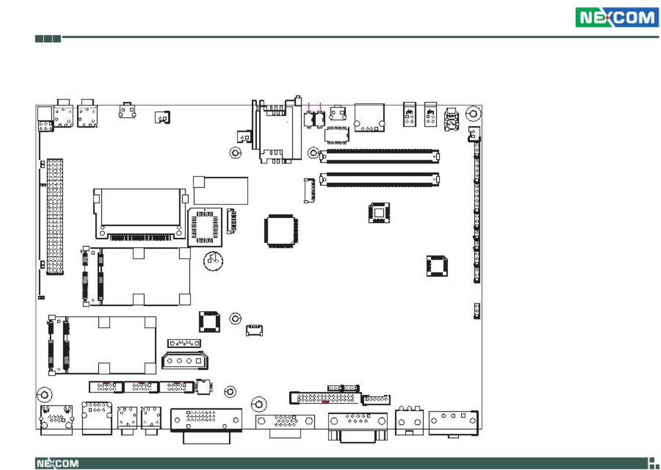
10
Appendix
C:
VTCB6110
Carrier
Board
Jumpers
and
Connectors
SW5SW4
SW2
J13
CN15
CN14
SW7
J11
J9
SW3
USB1
LED2
LED1
SW1
J2
J4
J1
CN17
CN4
JP6
J12
Blue
Tooth
J7
J3
JP5
JP4
J14
JP8
JP7
JP3
CN16
3.5G
BZ1
JP2
JP1
WLAN
CN6
J10
J8
CN12
CN9
CN7
SW6
J6
J5
LAN1
USB2
CN11
CN8
CN5
CON1
COM1
CN2
CN1
Copyright
©
2009
NEXCOM
International
Co.,
Ltd.
All
Rights
Reserved.
73
VTC
6110
User
Manual
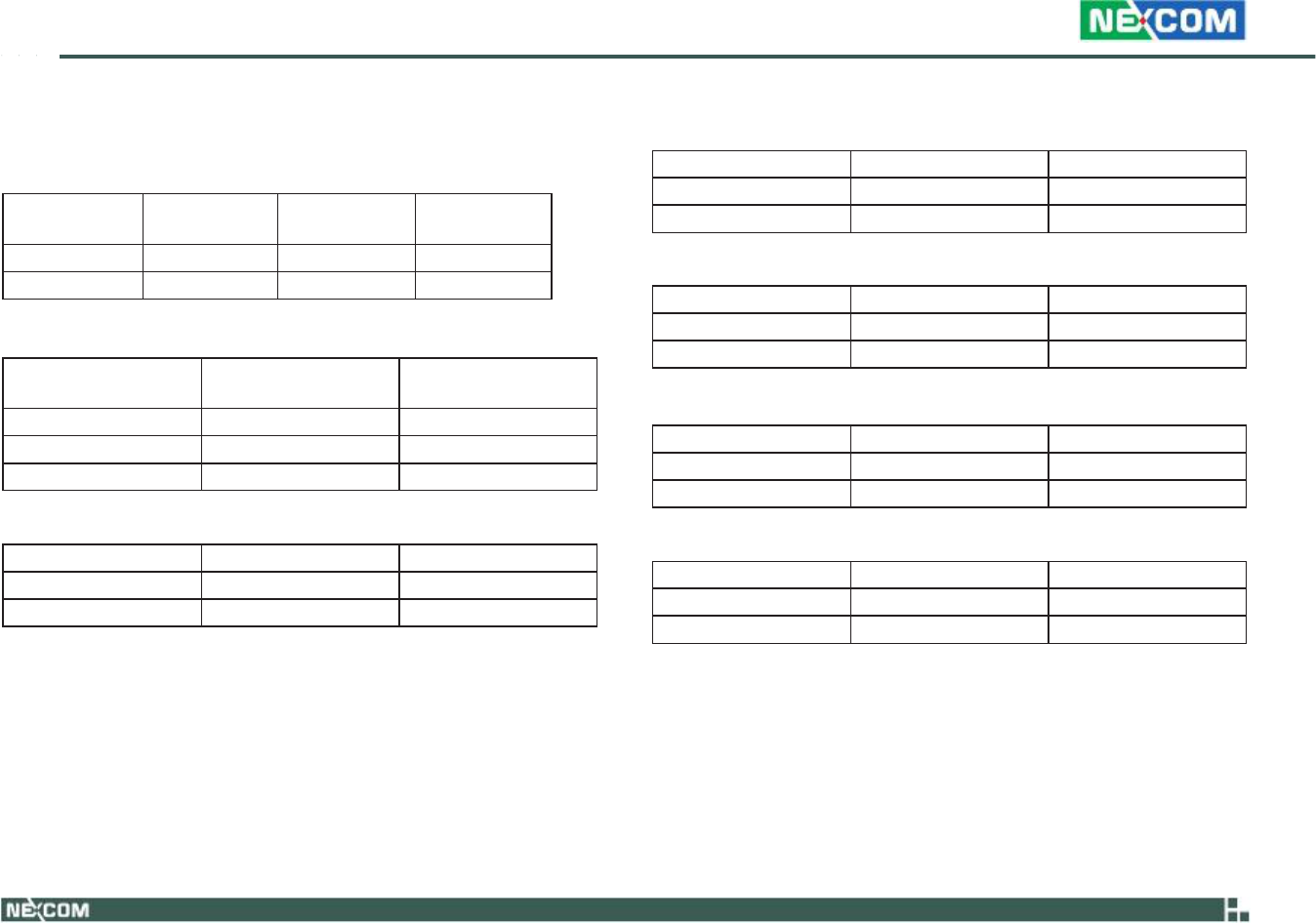
Appendix
C:
VTCB6110
Carrier
Board
Jumper
Settings
LVDS
Power
Input
Voltage
Select
(JP9)
SW5:
Input
Voltage
Selection
CMOS
Input
Voltage
Select
(J6)
SW6:
COM
Port
Mode
Selection
BIOS
Function
Select
(J1)
CF
(IDE0)
Primary
Master/Slave
Select
(JP4)
Copyright
©
2009
NEXCOM
International
Co.,
Ltd.
All
Rights
Reserved.
74
DC
Input
Voltage
Select
(JP1)
VTC
6110
User
Manual
SW6
COM
Port
Mode
RS232
(default)
RS485
SW6.1
OFF
ON
SW6.2
OFF
ON
SW6.3
OFF
ON
SW5
/
Input
Voltage
12V
(default)
24V
6V~36V
SW5.1
OFF
OFF
ON
SW5.2
OFF
ON
Ignore
Pin
Status
Function
Description
1-2
Short
Slave
2-3
(default)
Short
(default)
Master
Pin
Status
Function
Description
1-2
Short
+5V
IN
2-3
(default)
Short
(default)
+3.3V
IN
Pin
Status
Function
Description
1-2
(default)
Short
(default)
VBAT
IN
2-3
Short
Clear
CMOS
Pin
Status
Function
Description
1-2
Short
Disable
carrier
board
BIOS
2-3
(default)
Short
(default)
Disable
module
board
BIOS
Pin
Status
Function
Description
1-2
(default)
Short
(default)
IGNITION
2-3
Short
VIN_M
Appendix
C:
VTCB6110
Carrier
Board
Temp
Sensor
(JP8)
GAL
Download
(JP5)
Auto
Power
Select
(JP2)
MCU
COM
Port
(JP3)
PCI-104
VI/O
Select
Voltage
(J13)
MCU
Download
(JP6)
Copyright
©
2009
NEXCOM
International
Co.,
Ltd.
All
Rights
Reserved.
75
VTC
6110
User
Manual
Pin
Function
Description
1
+V3.3S
2
GND
3
TCK
4
TDO
5
TDI
6
TMS
Pin
Function
Description
1
+V3.3ALW
2
C2D
3
MRST
4
C2CK
5
GND
Pin
Function
Description
1
TX
2
RX
3
GND
Pin
Status
Function
Description
1-4(*)
Short*
+3.3V
3-6
Short
+5V
Pin
Function
Description
1
SENSOR+
2
GND
Pin
Status
Function
Description
1-2
(default)
Short
(default)
AUTO
2-3
Short
BUTTON
CONTROL
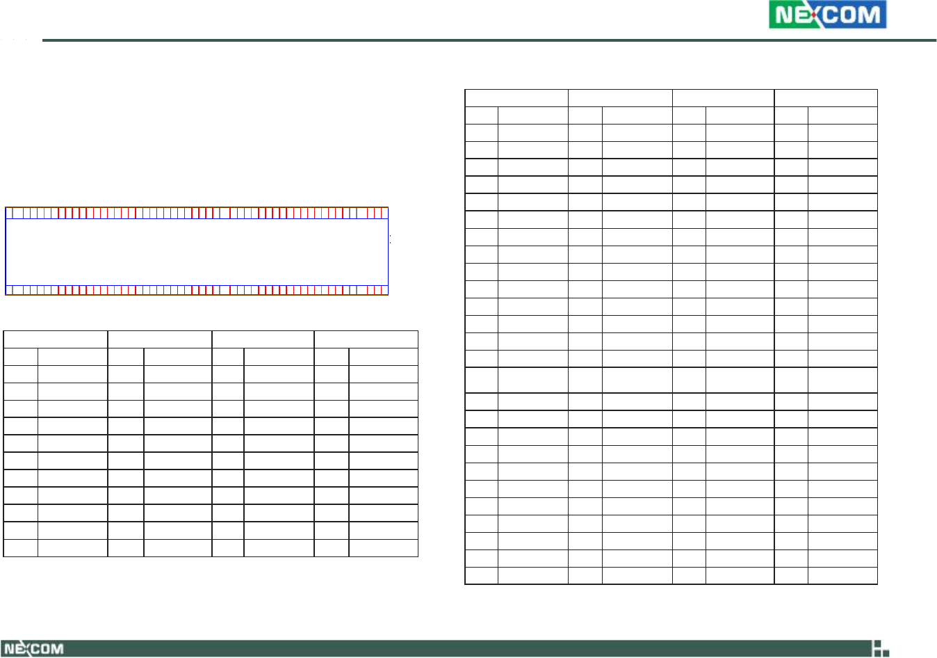
B1
B2
B3
B4
B5
B6
B7
B8
B9
B10
B11
B12
B13
B14
B15
B16
B17
B18
B19
B2
0
B21
B22
B23
B24
B25
B26
B27
B28
B29
B30
B31
B32
B33
B34
B35
B36
B37
B38
B39
B40
B41
B42
B43
B44
B45
B46
B47
B48
B49
B50
B51
B52
B53
B54
B55
B56
B57
B58
B59
B60
B61
B62
B63
B64
B65
B66
B67
B68
B69
B70
B71
B72
B73
B74
B75
B76
B77
B78
B79
B80
B81
B82
B83
B84
B85
B86
B87
B88
B89
B90
B91
B92
B93
B94
B95
B96
B97
B98
B99
B100
B101
B102
B103
B104
B105
B106
B107
B108
B109
B110
B1
B2
B3
B4
B5
B6
B7
B8
B9
B10
B11
B1
2
B13
B14
B15
B16
B17
B18
B19
B20
B21
B22
B23
B24
B25
B26
B27
B28
B29
B30
B31
B32
B33
B34
B35
B36
B37
B38
B39
B40
B41
B42
B43
B44
B45
B46
B47
B48
B49
B50
B51
B52
B53
B54
B55
B56
B57
B58
B59
B60
B61
B62
B63
B64
B65
B66
B67
B68
B69
B70
B71
B72
B73
B74
B75
B76
B77
B78
B79
B80
B81
B82
B83
B84
B85
B86
B87
B88
B89
B90
B91
B92
B93
B94
B95
B96
B97
B98
B99
B100
B101
B102
B103
B104
B105
B106
B107
B108
B109
B110
A1
A2
A3
A4
A5
A6
A7
A8
A9
A10
A11
A12
A13
A14
A15
A16
A17
A18
A19
A20
A21
A22
A23
A24
A25
A26
A27
A28
A29
A30
A31
A32
A33
A34
A35
A36
A37
A38
A39
A40
A41
A42
A43
A44
A45
A46
A47
A48
A49
A50
A51
A52
A53
A54
A55
A56
A57
A58
A59
A60
A61
A62
A63
A64
A65
A66
A67
A68
A69
A70
A71
A72
A73
A74
A75
A76
A77
A78
A79
A80
A81
A82
A83
A84
A85
A86
A87
A88
A89
A90
A91
A92
A93
A94
A95
A96
A97
A98
A99
A100
A101
A102
A103
A104
A105
A106
A107
A108
A109
A110
Appendix
C:
VTCB6110
Carrier
Board
Connectors
High
Speed
Board-to-Board
Connector:
COM
Express
Row
A
and
Row
B
Connector
size:
2
x
110
=
220
pins
Connector
location:
J4
J1
C OM E xp re ss
MH 2
MH 1
Connector
Pin
Definition
Copyright
©
2009
NEXCOM
International
Co.,
Ltd.
All
Rights
Reserved.
76
VTC
6110
User
Manual
Row
A
Row
B
Row
A
Row
B
A13
GBE0_MDI0+
B13
SMB_CK
A68
PCIE_TX0+
B68
PCIE_RX0+
A14
GBE0_CTREF
B14
SMB_DAT
A69
PCIE_TX0-
B69
PCIE_RX0-
A15
SUS_S3#
B15
SMB_ALERT#
A70
GND
B70
GND
A16
SATA0_TX+
B16
NC
A71
LVDS_A0+
B71
NC
A17
SATA0_TX-
B17
NC
A72
LVDS_A0-
B72
NC
A18
SUS_S4#
B18
SUS_STAT#
A73
LVDS_A1+
B73
NC
A19
SATA0_RX+
B19
NC
A74
LVDS_A1+
B74
NC
A20
SATA0_RX-
B20
NC
A75
LVDS_A2+
B75
NC
A21
GND
B21
GND
A76
LVDS_A2+
B76
NC
A22
NC
B22
NC
A77
LVDS_VDD_EN
B77
NC
A23
NC
B23
NC
A78
LVDS_A3+
B78
NC
A24
SUS_S5#
B24
PWR_OK
A79
LVDS_A3+
B79
LVDS_BKLT_EN
A25
NC
B25
NC
A80
GND
B80
GND
A26
NC
B26
NC
A81
LVDS_A_CK+
B81
NC
A27
BATLOW#
B27
NC
A82
LVDS_A_CK-
B82
NC
A28
ATA_ACT#
B28
NC
A83
LVDS_I2C_CK
B83
LVDS_BKLT_
CTRL
A29
AC_SYNC
B29
NC
A84
LVDS_I2C_DAT
B84
VCC_5V_SBY
A30
AC_RST#
B30
AC_SDIN0
A85
NC
B85
VCC_5V_SBY
A31
GND
B31
GND
A86
NC
B86
VCC_5V_SBY
A32
AC_BITCLK
B32
SPKR
A87
NC
B87
VCC_5V_SBY
A33
AC_SDOUT
B33
I2C_CK
A88
PCIE0_CK_REF+
B88
RSVD
A34
NC
B34
I2C_DAT
A89
PCIE0_CK_REF-
B89
NC
A35
NC
B35
THRM#
A90
GND
B90
GND
A36
USB6-
B36
NC
A91
RSVD
B91
NC
A37
USB6+
B37
NC
A92
RSVD
B92
NC
A38
USB_6_7_OC#
B38
USB_4_5_OC#
A93
NC
B93
NC
A39
USB4-
B39
USB5-
A94
RSVD
B94
NC
Row
A
Row
B
Row
A
Row
B
A1
GND
B1
GND
A56
NC
B56
NC
A2
GBE0_MDI3-
B2
GBE0_ACT#
A57
GND
B57
NC
A3
GBE0_MDI3+
B3
LPC_FRAME#
A58
NC
B58
NC
A4
NC
B4
LPC_AD0
A59
NC
B59
NC
A5
NC
B5
LPC_AD1
A60
GND
B60
GND
A6
GBE0_MDI2-
B6
LPC_AD2
A61
NC
B61
NC
A7
GBE0_MDI2+
B7
LPC_AD3
A62
NC
B62
NC
A8
GBE0_LINK#
B8
NC
A63
GPI1
B63
GPO3
A9
GBE0_MDI1-
B9
NC
A64
NC
B64
NC
A10
GBE0_MDI1+
B10
LPC_CLK
A65
NC
B65
NC
A11
GND
B11
GND
A66
GND
B66
NC
A12
GBE0_MDI0-
B12
PWRBTN#
A67
NC
B67
NC
Row
B
MH 2
MH
1
COM
Express
Connector
Row
A

Appendix
C:
VTCB6110
Carrier
Board
Copyright
©
2009
NEXCOM
International
Co.,
Ltd.
All
Rights
Reserved.
77
VTC
6110
User
Manual
Row
A
Row
B
Row
A
Row
B
A40
USB4+
B40
USB5+
A95
RSVD
B95
NC
A41
GND
B41
GND
A96
GND
B96
NC
A42
USB2-
B42
USB3-
A97
VCC_12V
B97
NC
A43
USB2+
B43
USB3+
A98
VCC_12V
B98
NC
A44
USB_2_3_OC#
B44
USB_0_1_OC#
A99
VCC_12V
B99
NC
A45
USB0-
B45
USB1-
A100
GND
B100
GND
A46
USB0+
B46
USB1+
A101
VCC_12V
B101
VCC_12V
A47
VCC_RTC
B47
NC
A102
VCC_12V
B102
VCC_12V
A48
NC
B48
NC
A103
VCC_12V
B103
VCC_12V
A49
NC
B49
SYS_RESET#
A104
VCC_12V
B104
VCC_12V
A50
NC
B50
CB_RESET#
A105
VCC_12V
B105
VCC_12V
A51
GND
B51
GND
A106
VCC_12V
B106
VCC_12V
A52
NC
B52
NC
A107
VCC_12V
B107
VCC_12V
A53
NC
B53
NC
A108
VCC_12V
B108
VCC_12V
A54
NC
B54
NC
A109
VCC_12V
B109
VCC_12V
A55
NC
B55
NC
A110
GND
B110
GND
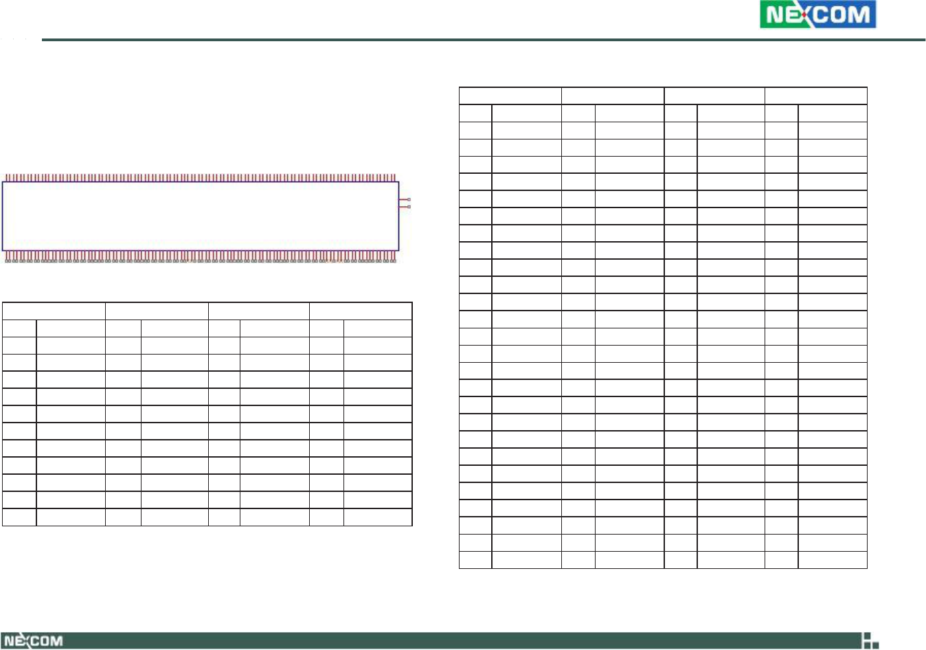
B1
B2
B3
B4
B5
B6
B7
B8
B9
B10
B11
B12
B13
B14
B15
B16
B17
B18
B19
B20
B21
B22
B23
B24
B25
B26
B27
B28
B29
B30
B31
B32
B33
B34
B35
B36
B37
B38
B39
B40
B41
B42
B43
B44
B45
B46
B47
B48
B49
B50
B51
B52
B53
B54
B55
B56
B57
B58
B59
B60
B61
B62
B63
B64
B65
B66
B67
B68
B69
B70
B71
B72
B73
B74
B75
B76
B77
B78
B79
B80
B81
B82
B83
B84
B85
B86
B87
B88
B89
B90
B91
B92
B93
B94
B95
B96
B97
B98
B99
B100
B101
B102
B103
B104
B105
B106
B107
B108
B109
B110
A1
A2
A3
A4
A5
A6
A7
A8
A9
A10
A11
A12
A13
A14
A15
A16
A17
A18
A19
A20
A21
A22
A23
A24
A25
A26
A27
A28
A29
A30
A31
A32
A33
A34
A35
A36
A37
A38
A39
A40
A41
A42
A43
A44
A45
A46
A47
A48
A49
A50
A51
A52
A53
A54
A55
A56
A57
A58
A59
A60
A61
A62
A63
A64
A65
A66
A67
A68
A69
A70
A71
A72
A73
A74
A75
A76
A77
A78
A79
A80
A81
A82
A83
A84
A85
A86
A87
A88
A89
A90
A91
A92
A93
A94
A95
A96
A97
A98
A99
A100
A101
A102
A103
A104
A105
A106
A107
A108
A109
A110
Appendix
C:
VTCB6110
Carrier
Board
High
Speed
Board-to-Board
Connector:
COM
Express
Row
C
and
Row
D
Connector
size:
2
X
110
=
220
Pins
Connector
location:
J3
J1
C OM E xpre s s
Row
D
COM
Express
Connector
MH2
MH2
MH1
MH1
Row
C
Connector
Pin
Definition
Copyright
©
2009
NEXCOM
International
Co.,
Ltd.
All
Rights
Reserved.
78
VTC
6110
User
Manual
Row
C
Row
D
Row
C
Row
D
C13
IDE_IORDY
D13
IDE_A0
C68
NC
D68
NC
C14
IDE_IOR#
D14
IDE_A1
C69
NC
D69
NC
C15
NC
D15
IDE_A2
C70
GND
D70
GND
C16
NC
D16
IDE_CS1#
C71
NC
D71
NC
C17
NC
D17
IDE_CS3#
C72
NC
D72
NC
C18
NC
D18
IDE_RESET#
C73
NC
D73
SDVO_CLK
C19
NC
D19
NC
C74
NC
D74
NC
C20
PCI_GNT0#
D20
NC
C75
NC
D75
NC
C21
GND
D21
GND
C76
GND
D76
GND
C22
PCI_REQ0#
D22
PCI_AD1
C77
NC
D77
IDE_CBLID#
C23
PCI_RESET#
D23
PCI_AD3
C78
NC
D78
NC
C24
PCI_AD0
D24
PCI_AD5
C79
NC
D79
NC
C25
PCI_AD2
D25
PCI_AD7
C80
GND
D80
GND
C26
PCI_AD4
D26
PCI_C/BE0#
C81
NC
D81
NC
C27
PCI_AD6
D27
PCI_AD9
C82
NC
D82
NC
C28
PCI_AD8
D28
PCI_AD11
C83
NC
D83
NC
C29
PCI_AD10
D29
PCI_AD13
C84
GND
D84
GND
C30
PCI_AD12
D30
PCI_AD15
C85
NC
D85
NC
C31
GND
D31
GND
C86
NC
D86
NC
C32
PCI_AD14
D32
PCI_PAR
C87
GND
D87
GND
C33
PCI_C/BE1#
D33
PCI_SERR#
C88
NC
D88
NC
C34
PCI_PERR#
D34
PCI_STOP#
C89
NC
D89
NC
C35
PCI_LOCK#
D35
PCI_TRDY#
C90
GND
D90
GND
C36
PCI_DEVSEL#
D36
PCI_FRAME#
C91
NC
D91
NC
C37
PCI_IRDY#
D37
PCI_AD16
C92
NC
D92
NC
C38
PCI_C/BE2#
D38
PCI_AD18
C93
GND
D93
GND
C39
PCI_AD17
D39
PCI_AD20
C94
NC
D94
NC
Row
C
Row
D
Row
C
Row
D
C1
GND
D1
GND
C56
NC
D56
SDVOB_GREEN-
C2
IDE_D7
D2
IDE_D5
C57
NC
D57
NC
C3
IDE_D6
D3
IDE_D10
C58
NC
D58
SDVOB_BLUE+
C4
IDE_D3
D4
IDE_D11
C59
NC
D59
SDVOB_BLUE-
C5
IDE_D15
D5
IDE_D12
C60
GND
D60
GND
C6
IDE_D8
D6
IDE_D4
C61
NC
D61
SDVO_CLK+
C7
IDE_D9
D7
IDE_D0
C62
NC
D62
SDVO_CLK-
C8
IDE_D2
D8
IDE_REQ
C63
NC
D63
NC
C9
IDE_D13
D9
IDE_IOW#
C64
NC
D64
NC
C10
IDE_D1
D10
IDE_ACK#
C65
NC
D65
NC
C11
GND
D11
GND
C66
NC
D66
NC
C12
IDE_D14
D12
IDE_IRQ
C67
NC
D67
GND

Appendix
C:
VTCB6110
Carrier
Board
Copyright
©
2009
NEXCOM
International
Co.,
Ltd.
All
Rights
Reserved.
79
VTC
6110
User
Manual
Row
C
Row
D
Row
C
Row
D
C40
PCI_AD19
D40
PCI_AD22
C95
PEG_RX13-
D95
PEG_TX13-
C41
GND
D41
GND
C96
GND
D96
GND
C42
PCI_AD21
D42
PCI_AD24
C97
RSVD
D97
PEG_ENABLE#
C43
PCI_AD23
D43
PCI_AD26
C98
PEG_RX14+
D98
PEG_TX14+
C44
PCI_C/BE3#
D44
PCI_AD28
C99
PEG_RX14-
D99
PEG_TX14-
C45
PCI_AD25
D45
PCI_AD30
C100
GND
D100
GND
C46
PCI_AD27
D46
PCI_IRQC#
C101
PEG_RX15+
D101
PEG_TX15+
C47
PCI_AD29
D47
PCI_IRQD#
C102
PEG_RX15-
D102
PEG_TX15-
C48
PCI_AD31
D48
PCI_CLKRUN#
C103
GND
D103
GND
C49
PCI_IRQA#
D49
PCI_M66EN
C104
VCC_12V
D104
VCC_12V
C50
PCI_IRQB#
D50
PCI_CLK
C105
VCC_12V
D105
VCC_12V
C51
GND
D51
GND
C106
VCC_12V
D106
VCC_12V
C52
PEG_RX0+
D52
PEG_TX0+
C107
VCC_12V
D107
VCC_12V
C53
PEG_RX0-
D53
PEG_TX0-
C108
VCC_12V
D108
VCC_12V
C54
TYPE0#
D54
PEG_LANE_RV#
C109
VCC_12V
D109
VCC_12V
C55
PEG_RX1+
D55
PEG_TX1+
C110
GND
D110
GND
49
Appendix
C:
VTCB6110
Carrier
Board
CompactFlash
Connector
Connector
size:
2
x
25
=
50
pins
Connector
location:
J12
50
26
1
Connector
Pin
Definition
Copyright
©
2009
NEXCOM
International
Co.,
Ltd.
All
Rights
Reserved.
80
VTC
6110
User
Manual
Pin
Description
Pin
Description
23
Data
2
24
IOCS16#
(NC)
25
CF_CD2#
(Pull-down)
26
CF_CD1#
(Pull-down)
27
Data
11
28
Data
12
29
Data
13
30
Data
14
31
Data
15
32
HDC
CS300
33
CF_VS1#
(NC)
34
IOR
35
IOW
36
CF_WE#
(+5V)
37
Interrupt
15
38
+5V
39
CF_CSEL#
(Master
or
Slave)
40
CF_VS2#
(NC)
41
Reset
#
42
IOCHRDY
43
DMA
REQ
/
DACK
(NC)
44
DMA
ACK#
/CF_REG#
(+5V)
45
HDD
Active
Led
46
DMA66
Detect
/
CF_PDIAG#
47
Data
8
48
Data
9
49
Data
10
50
Gnd
Pin
Description
Pin
Description
1
Gnd
2
Data
3
3
Data
4
4
Data
5
5
Data
6
6
Data
7
7
HDC
CS100
8
Gnd
9
Gnd
10
Gnd
11
Gnd
12
Gnd
13
+5V
14
Gnd
15
Gnd
16
Gnd
17
Gnd
18
Disk
Address
2
19
Disk
Address
1
20
Disk
Address
0
21
Data
0
22
Data
1

3 42
Appendix
C:
VTCB6110
Carrier
Board
GPIO
Connector
Connector
size:
DSUB-9
pin
Connector
location:
COM1
5
1
9
6
Connector
Pin
Definition
Copyright
©
2009
NEXCOM
International
Co.,
Ltd.
All
Rights
Reserved.
81
RS232
Connector:
COM1,
COM2
Connector
size:
2
x
10
=
20
Pins
Pin
Header,
(2.0
mm
Pitch)
Connector
location:
COM1
(CN9),
COM2
(CN7)
CN10
1
5
6
7
8
9
10
BOX-2.0mm-M-180
Connector
Pin
Definition
VTC
6110
User
Manual
Pin
Definition
Pin
Definition
1
DCD
2
RXD
3
TXD
4
DTR
5
Gnd
6
DSR
7
RTS
8
CTS
9
RI
Pin
Description
Pin
Description
1
GIN1
2
GIN2
3
GIN3
4
GIN4
5
GOUT4
6
GOUT1
7
GOUT2
8
GOUT3
9
GND

3 42
Appendix
C:
VTCB6110
Carrier
Board
RS232/485
Connector:
COM3
Connector
size:
2
x
10
=
20
Pins
Pin
Header,
(2.0
mm
Pitch)
Connector
location:
CN12
GAL
Programmer
PIN
Header
Connector
size:
2.54mm-M-180
Connector
location:
JP5
CN10
1
5
6
7
8
9
10
BOX-2.0mm-M-180
1
2
3
4
5
6
JP5
PIN-2.54mm-M-180
Connector
Pin
Definition
Copyright
©
2009
NEXCOM
International
Co.,
Ltd.
All
Rights
Reserved.
82
Connector
Pin
Definition
VTC
6110
User
Manual
Pin
Definition
Pin
Definition
1
DCD
(RS232)
TX-/RX-
(RS485)
2
RXD
(RS232)
TX+/RX+
(RS485)
3
TXD
(RS232)
4
DTR
(RS232)
5
Gnd
6
DSR
(RS232)
7
RTS
(RS232)
8
CTS
(RS232)
9
RI
(RS232)
Pin
Definition
Pin
Definition
1
+3.3V
2
GND
3
TCK
4
TDO
5
TDI
6
TMS

Appendix
C:
VTCB6110
Carrier
Board
MCU
Programmer
Pin
Header
Connector
size:
2.54mm-M-180
Connector
location:
JP6
VGA
Connector
Connector
size:
DSUB-15
Connector
location:
CON1
1
2
3
4
5
JP6
PIN-2.54mm-M-180
Connector
Pin
Definition
Copyright
©
2009
NEXCOM
International
Co.,
Ltd.
All
Rights
Reserved.
83
Connector
Pin
Definition
VTC
6110
User
Manual
Pin
Definition
Pin
Definition
1
RED
2
GREEN
3
BLUE
4
NC
5
Gnd
6
Gnd
7
Gnd
8
Gnd
9
VCC
10
Gnd
11
NC
12
DDCDAT
13
Hsync
14
Vsync
15
DDCCLK
Pin
Definition
Pin
Definition
1
+3.3ALW
2
C2D
3
MRST
4
C2CK
5
GND

3
42
11
10
Appendix
C:
VTCB6110
Carrier
Board
LVDS
Connector
+
USB0
Connector
size:
2
x
15
(2.0mm)
Connector
location:
CN3
CN3
1
5
6
7
8
9
12
13
14
15
16
17
18
19
20
21
22
23
24
25
26
27
28
29
30
BOX-2.0mm-M-180
Connector
Pin
Definition
Copyright
©
2009
NEXCOM
International
Co.,
Ltd.
All
Rights
Reserved.
84
VTC
6110
User
Manual
Pin
Definition
Pin
Definition
1
LVDS_CLK
2
LVDS_DAT
3
Panel_VDD
4
LVDS_1(OUT0)
5
LVDS_9(OUT3)
6
LVDS_0(OUT0#)
7
LVDS_8(OUT3#)
8
Panel_VDD
9
LVDS_GND
10
LVDS_GND
11
LVDS_7(CLK)
12
LVDS_3(OUT1)
13
LVDS_6(CLK#)
14
LVDS_2(OUT1#)
15
LVDS_GND
16
LVDS_GND
Pin
Definition
Pin
Definition
17
LVDS_5(OUT2)
18
Panel_backlight(+12V)
19
LVDS_4(OUT2#)
20
Panel_backlight(+12V)
21
LVDS_GND
22
Power
on
push
buttom
23
USB_0#
24
USB_GND
25
USB_0
26
USB_VCC
(+5V)
27
USB_GND
28
USB_GND
29
Panel_backlight(+12V)
30
GND
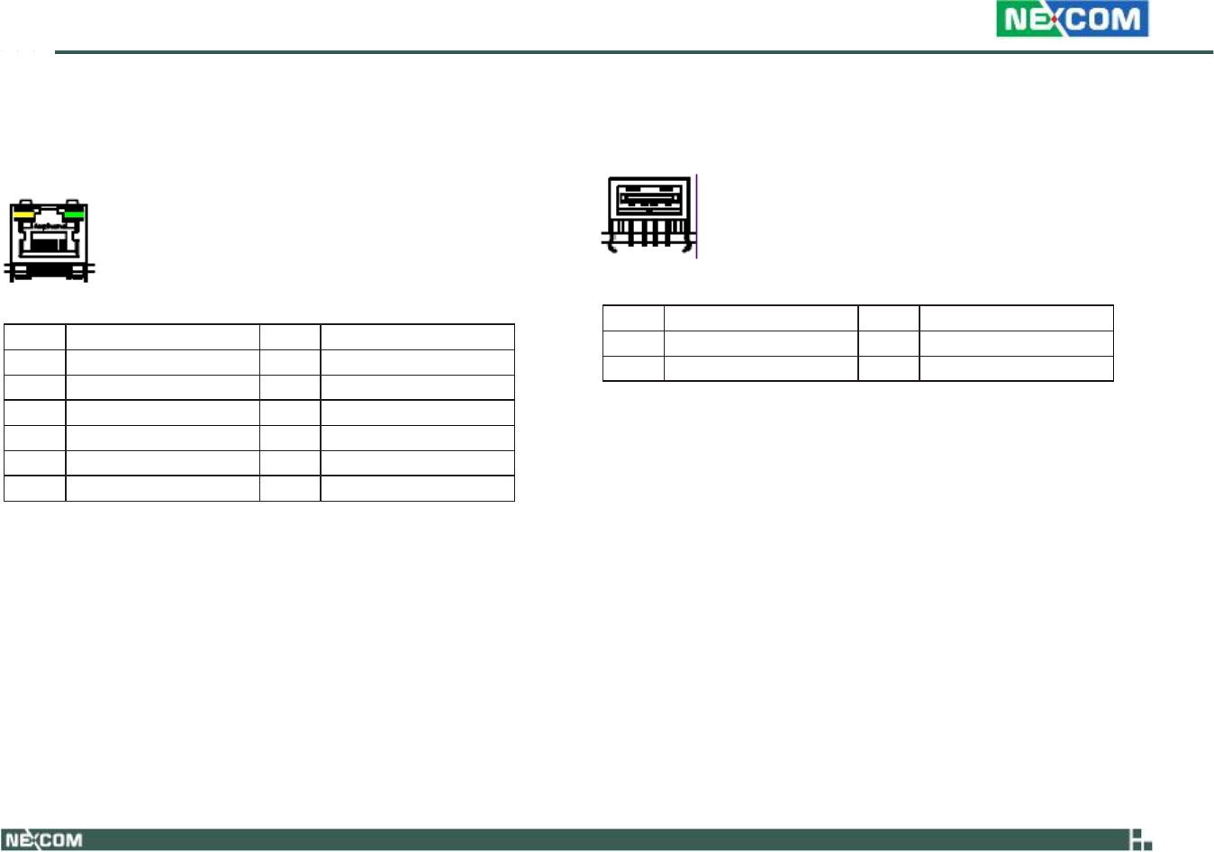
Appendix
C:
VTCB6110
Carrier
Board
LAN
Connector
Connector
size:
RJ-45
USB
Connector
Connector
location:
USB1
Connector
location:
LAN1
Connector
Pin
Definition
Connector
Pin
Definition
Copyright
©
2009
NEXCOM
International
Co.,
Ltd.
All
Rights
Reserved.
85
VTC
6110
User
Manual
Pin
Definition
Pin
Definition
1
TX+
2
TX-
3
RX+
4
N/C1
5
N/C2
6
RX-
7
N/C3
8
N/C4
9
LAN
Speed
LED
10
+3.3V
11
LAN
Link
LED
12
+3.3V
Pin
Definition
Pin
Definition
1
VCC
2
DATA-
3
DATA+
4
GND
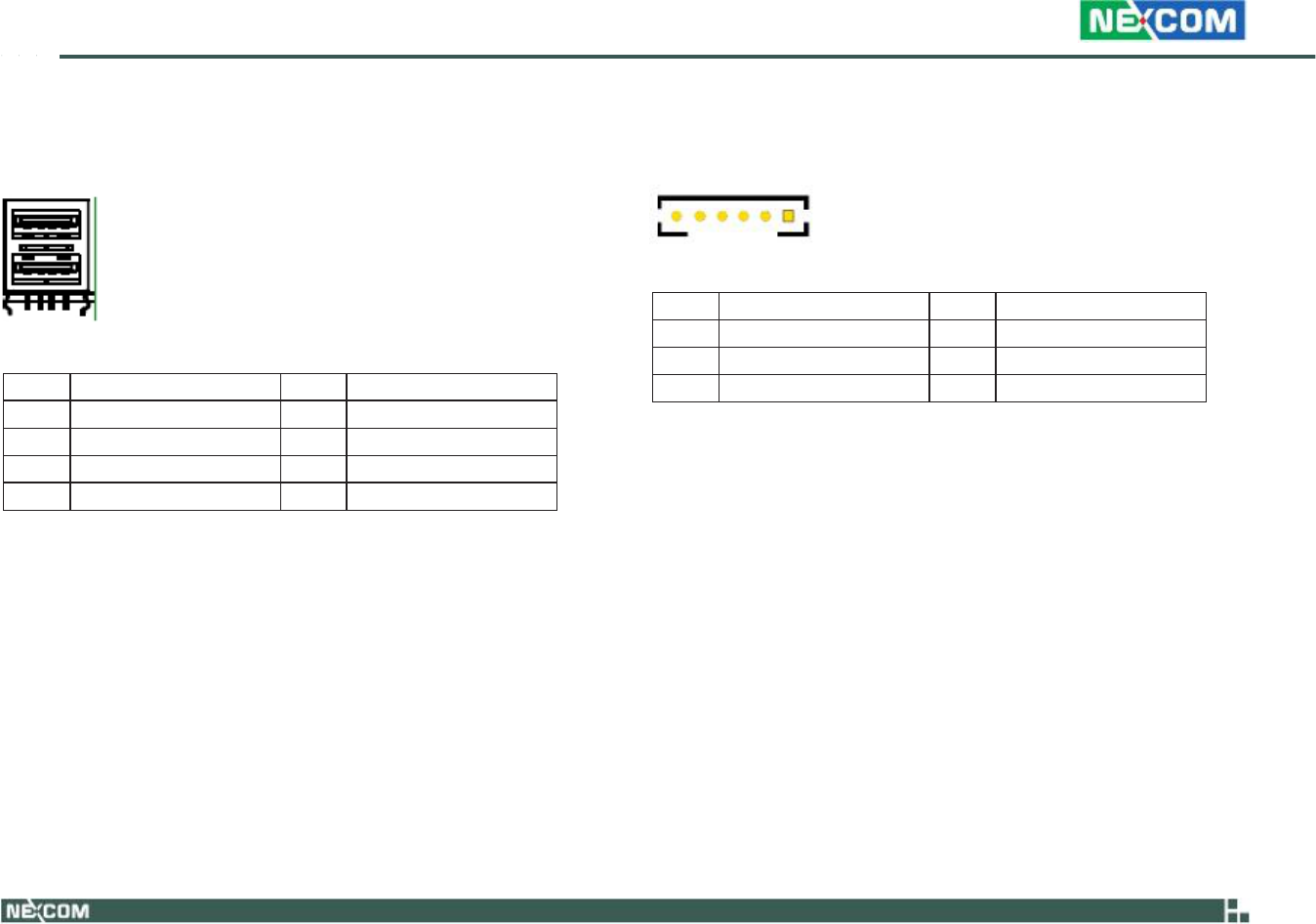
Appendix
C:
VTCB6110
Carrier
Board
USB
Connector
Connector
location:
USB2
LVDS
Power
Connector
Connector
location:
J5
1
Connector
Pin
Definition
Connector
Pin
Definition
Copyright
©
2009
NEXCOM
International
Co.,
Ltd.
All
Rights
Reserved.
86
VTC
6110
User
Manual
Pin
Definition
Pin
Definition
1
VCC
2
DATA1-
3
DATA1+
4
GND
5
VCC
6
DATA-
7
DATA+
8
GND
Pin
Definition
Pin
Definition
1
Panel_backlight
2
Panel_VDD
3
GND
4
GND
5
LVDS_PANEL
6
LVDS_BIASON
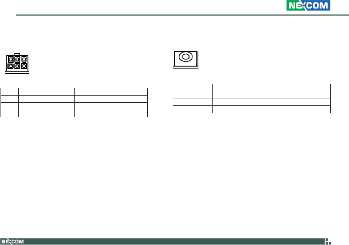
Appendix
C:
VTCB6110
Carrier
Board
External
12V
&
5V
Power
and
SMBUS
Connector
Connector
location:
CN2
Mic-in
Connector
location:
CN11
and
CN15
6
3
4
1
Connector
Pin
Definition
FOR AT&T NO This Function
Copyright
©
2009
NEXCOM
International
Co.,
Ltd.
All
Rights
Reserved.
87
Connector
Pin
Definition
VTC
6110
User
Manual
Pin
Definition
Pin
Definition
1
NC
2
MIC_JD
3
NC
4
MIC_OUT
5
GND
6
GND
Pin
Definition
Pin
Definition
1
5V
2
12V
3
SMBCLK
4
GND
5
GND
6
SMBDATA

Appendix
C:
VTCB6110
Carrier
Board
Line-out
Connector
location:
CN8
and
CN14
PCI-104
VI/O
Voltage
Setting
Connector
location:
J13
2
4
6
Connector
Pin
Definition
1
3
5
Connector
Pin
Definition
Copyright
©
2009
NEXCOM
International
Co.,
Ltd.
All
Rights
Reserved.
88
VTC
6110
User
Manual
Pin
Definition
Pin
Definition
1
LINE_OUT_L
2
SURR_JD
3
NC
4
LINE_OUT_R
5
GND
6
GND
Pin
No.
Status
Function
Description
1-3,
2-4
(default)
Short
+3.3V
3-5,
4-6
Short
+5V

Appendix
C:
VTCB6110
Carrier
Board
PCI-104
Connector
Connector
location:
CN16
Connector
Pin
Definition
Copyright
©
2009
NEXCOM
International
Co.,
Ltd.
All
Rights
Reserved.
89
Power
Button
Connector
location:
SW1
Reset
Button
Connector
location:
SW2
VTC
6110
User
Manual
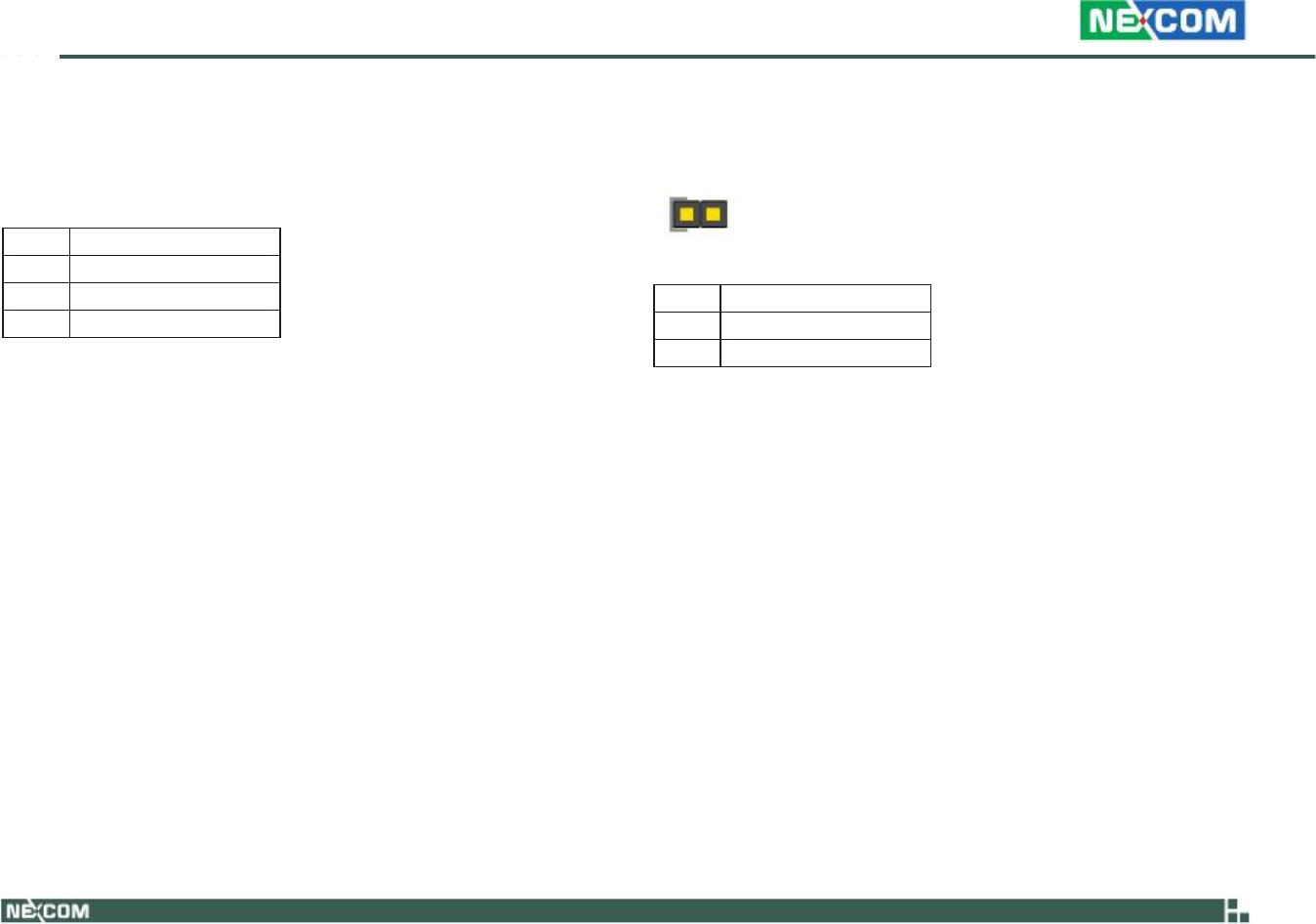
Appendix
C:
VTCB6110
Carrier
Board
MCU
COM
Port
Connector
location:
JP3
Connector
Pin
Definition
Copyright
©
2009
NEXCOM
International
Co.,
Ltd.
All
Rights
Reserved.
90
ACC_ON
LED
Connector
location:
JP7
1
Connector
Pin
Definition
VTC
6110
User
Manual
Pin
Function
Description
1
TX
2
RX
3
GND
Pin
Function
Description
1
+3.3V
LED
2
GND

Appendix
C:
VTCB6110
Carrier
Board
Temp
Sensor
Connector
location:
JP8
DC
Power
Input
Connector
Connector
location:
CN1
1
Connector
Pin
Definition
Connector
Pin
Definition
Copyright
©
2009
NEXCOM
International
Co.,
Ltd.
All
Rights
Reserved.
91
VTC
6110
User
Manual
Pin
Function
Description
1
GND
2
VIN
(6V~36V)
3
IGNITION
Pin
Function
Description
1
SENSOR+
2
GND
Appendix
C:
VTCB6110
Carrier
Board
Power
On
and
IDE
Active
LED
Connector
location:
LED1
T1
B1
Connector
Pin
Definition
Copyright
©
2009
NEXCOM
International
Co.,
Ltd.
All
Rights
Reserved.
92
GPIO
and
UMTS
LEDs
Connector
location:
LED2
T2
B2
LED
I/O
Port
Address
and
Data
VTC
6110
User
Manual
LED
Function
Description
T2
I/O
PORT
Address:
0EE0;
Bit0:
1
(Light),
0
(Dark)
B2
UMTS
STATUS
LED
Function
Description
T1
POWER
LED
B1
HD
LED

Appendix
C:
VTCB6110
Carrier
Board
Serial
ATA
Connector
location:
CN6
Serial
ATA
Power
Input
Connector
location:
J10
7
1
4
1
Connector
Pin
Definition
Copyright
©
2009
NEXCOM
International
Co.,
Ltd.
All
Rights
Reserved.
93
Connector
Pin
Definition
VTC
6110
User
Manual
Pin
Definition
Pin
Definition
1
GND
2
SATA_TXP0
-
3
SATA_TXN0
4
GND
5
SATA_RXN0
6
SATA_RXP0
7
GND
Pin
Definition
Pin
Definition
1
+V12S
2
GND
3
GND
4
+V5S
Appendix
C:
VTCB6110
Carrier
Board
Mini-PCIe
Socket
(for
3.5G
module)
PCIe
Interface
Connector
location:
CN10
Mini-PCIe
Socket
(for
WLAN
module)
USB
+
PCIe
Interface
Connector
location:
CN13
2
1
52
51
2
1
52
51
Connector
Pin
Definition
Copyright
©
2009
NEXCOM
International
Co.,
Ltd.
All
Rights
Reserved.
94
Connector
Pin
Definition
VTC
6110
User
Manual
Pin
Definition
Pin
Definition
Pin
Definition
Pin
Definition
1
MIC
+
2
+V3.3S
27
GND
28
NC
3
MIC
-
4
GND
29
GND
30
NC
5
SPK
+
6
NC
31
NC
32
NC
7
GND
8
USIM
PWR
33
RESET
34
GND
9
GND
10
USIM
DATa
35
GND
36
USB_D-
11
VCC_
MSM26_
DIG
12
USIM
CLK
37
GND
38
USB_D+
13
NC
14
USIM
RST
39
+V3.3S
40
GND
15
GND
16
NC
41
+V3.3S
42
LED_
WWAN#
17
NC
18
GND
43
GND
44
NC
19
NC
20
W_DIS-
ABLE#
45
NC
46
NC
21
GND
22
NC
47
NC
48
NC
23
NC
24
NC
49
NC
50
GND
25
NC
26
GND
51
NC
52
+V3.3S
Pin
Definition
Pin
Definition
Pin
Definition
Pin
Definition
1
WAKE#
2
+V3.3S
27
GND
28
+V1.5S
3
NC
4
GND
29
GND
30
SMB_CLK
5
NC
6
+V1.5S
31
PETn0
32
SMB_DATA
7
CLKREQ#
8
NC
33
PETp0
34
GND
9
GND
10
NC
35
GND
36
USB_D-
11
REFCLK-
12
NC
37
NC
38
USB_D+
13
REFCLK+
14
NC
39
NC
40
GND
15
GND
16
NC
41
NC
42
LED_
WWAN#
17
NC
18
GND
43
NC
44
LED_
WLAN#
19
NC
20
DISABLE#
45
NC
46
LED_
WPAN#
21
GND
22
PERST#
47
NC
48
+V1.5S
23
PERn0
24
+3.3S
49
NC
50
GND
25
PERp0
26
GND
51
NC
52
+V3.3S
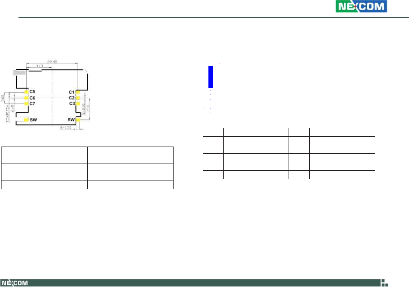
MH2
MH1
Appendix
C:
VTCB6110
Carrier
Board
SIM
Card
Connector
Connector
location:
CN4
Bluetooth
Connector
Connector
location:
J7
1
2
3
4
5
6
7
8
109
J7
Connector
Pin
Definition
Copyright
©
2009
NEXCOM
International
Co.,
Ltd.
All
Rights
Reserved.
95
VTC
6110
User
Manual
Pin
Definition
Pin
Definition
1
GND
2
USB_6P_L
3
USB_6N_L
4
NC
5
NC
6
BT_AUDIO_EN_R
7
NC
8
BT_3.3V
9
NC
10
GND
Pin
Definition
Pin
Definition
C1
POWER
VOLTAGE
C2
RESET
SIGNAL
C3
CLOCK
SIGNAL
C5
GND
C6
VPP:PROGRAM
VOLTAGE
C7
I/O
SW
Contact
present
switch
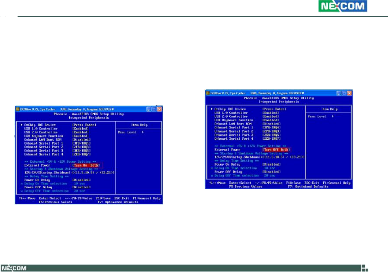
Appendix
D:
BIOS
Setup
A
PPENDIX
D:
V
EHICLE
P
OWER
M
ANAGEMENT
S
ETUP
External
Power
Output
Setting
External
+12V
and
+5V
Turn
Off
Simultaneously
External
+12V
and
+5V
Turn
On
Simultaneously
Copyright
©
2009
NEXCOM
International
Co.,
Ltd.
All
Rights
Reserved.
96
VTC
6110
User
Manual
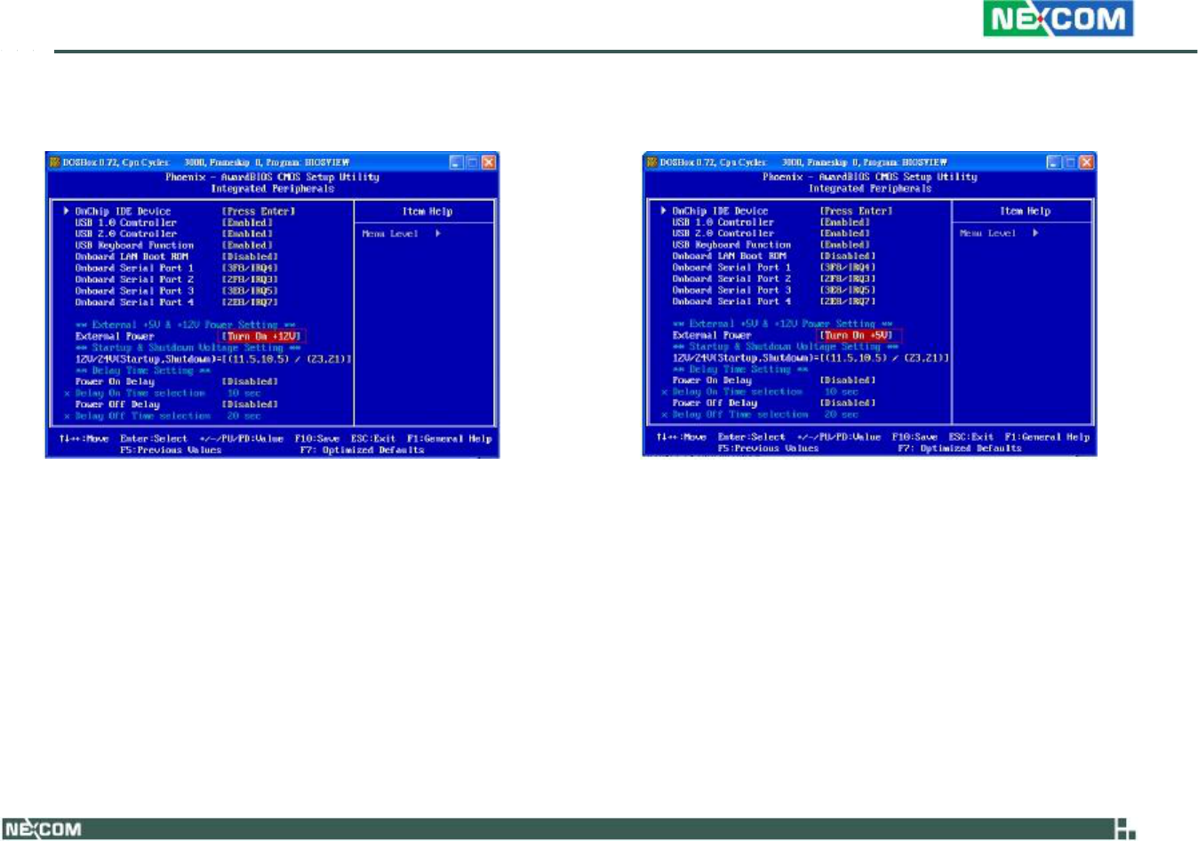
Appendix D: BIOS Setup
External
+12V
Turn
On
Only
External
+5V
Turn
On
Only
Copyright
©
2009
NEXCOM
International
Co.,
Ltd.
All
Rights
Reserved.
97
VTC
6110
User
Manual
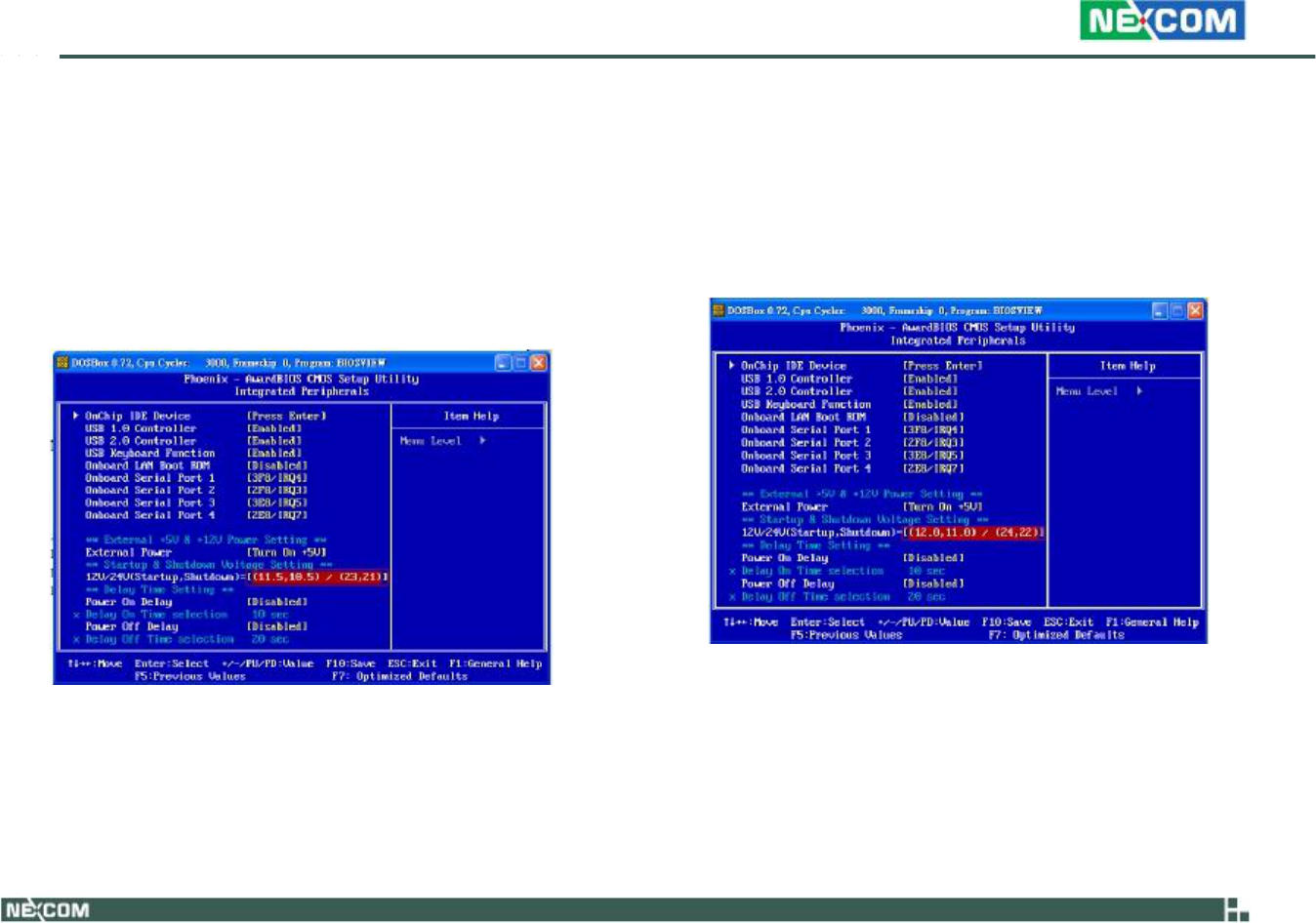
Appendix
D:
BIOS
Setup
Startup
and
Shutdown
Voltage
Setting
1.
If
the
input
voltage
setting
is
12V:
set
the
startup
voltage
to
11.5V
and
the
shutdown
voltage
to
10.5V.
If
the
input
voltage
setting
is
24V:
set
the
startup
voltage
to
23V
and
the
shutdown
voltage
to
21V.
2.
If
the
input
voltage
setting
is
12V:
set
the
startup
voltage
to
12V
and
the
shutdown
voltage
to
11V.
If
the
input
voltage
setting
is
24V:
set
the
startup
voltage
to
24V
and
the
shutdown
voltage
to
22V.
If
the
input
voltage
setting
is
6V~36V,
ignore
the
startup/shutdown
set-
ting.
If
the
input
voltage
setting
is
6V~36V,
ignore
the
startup/shutdown
set-
ting.
Copyright
©
2009
NEXCOM
International
Co.,
Ltd.
All
Rights
Reserved.
98
VTC
6110
User
Manual
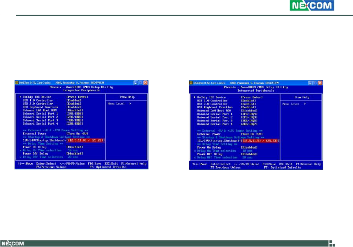
Appendix
D:
BIOS
Setup
3.
If
the
input
voltage
setting
is
12V:
set
the
startup
voltage
to
12.5V
and
the
shutdown
voltage
to
11V.
If
the
input
voltage
setting
is
24V:
set
the
startup
voltage
to
25V
and
the
shutdown
voltage
to
22V.
If
the
input
voltage
setting
is
6V~36V,
ignore
the
startup/shutdown
set-
ting.
4.
If
the
input
voltage
setting
is
12V:
set
the
startup
voltage
to
12.5V
and
the
shutdown
voltage
to
11.5V.
If
input
voltage
setting
is
24V:
set
the
startup
voltage
to
25V
and
the
shutdown
voltage
to
23V.
If
the
input
voltage
setting
is
6V~36V
ignore
the
startup/shutdown
set-
ting.
Copyright
©
2009
NEXCOM
International
Co.,
Ltd.
All
Rights
Reserved.
99
VTC
6110
User
Manual

Appendix
D:
BIOS
Setup
Power-on
Delay
Setting
Disable
Power-on
Delay
Enable
Power-on
Delay
Delay
time
can
be
set
at
10sec/30sec/1min./5min./10min./15min./30min./
1hour.
Copyright
©
2009
NEXCOM
International
Co.,
Ltd.
All
Rights
Reserved.
100
VTC
6110
User
Manual
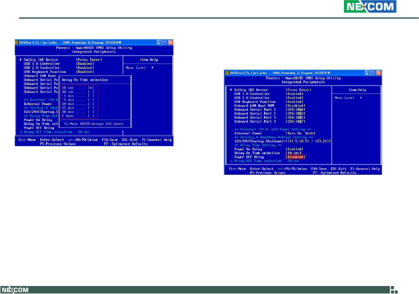
Appendix D: BIOS Setup
Power-off
Delay
Setting
Disable
Power-off
Delay
Copyright
©
2009
NEXCOM
International
Co.,
Ltd.
All
Rights
Reserved.
101
VTC
6110
User
Manual
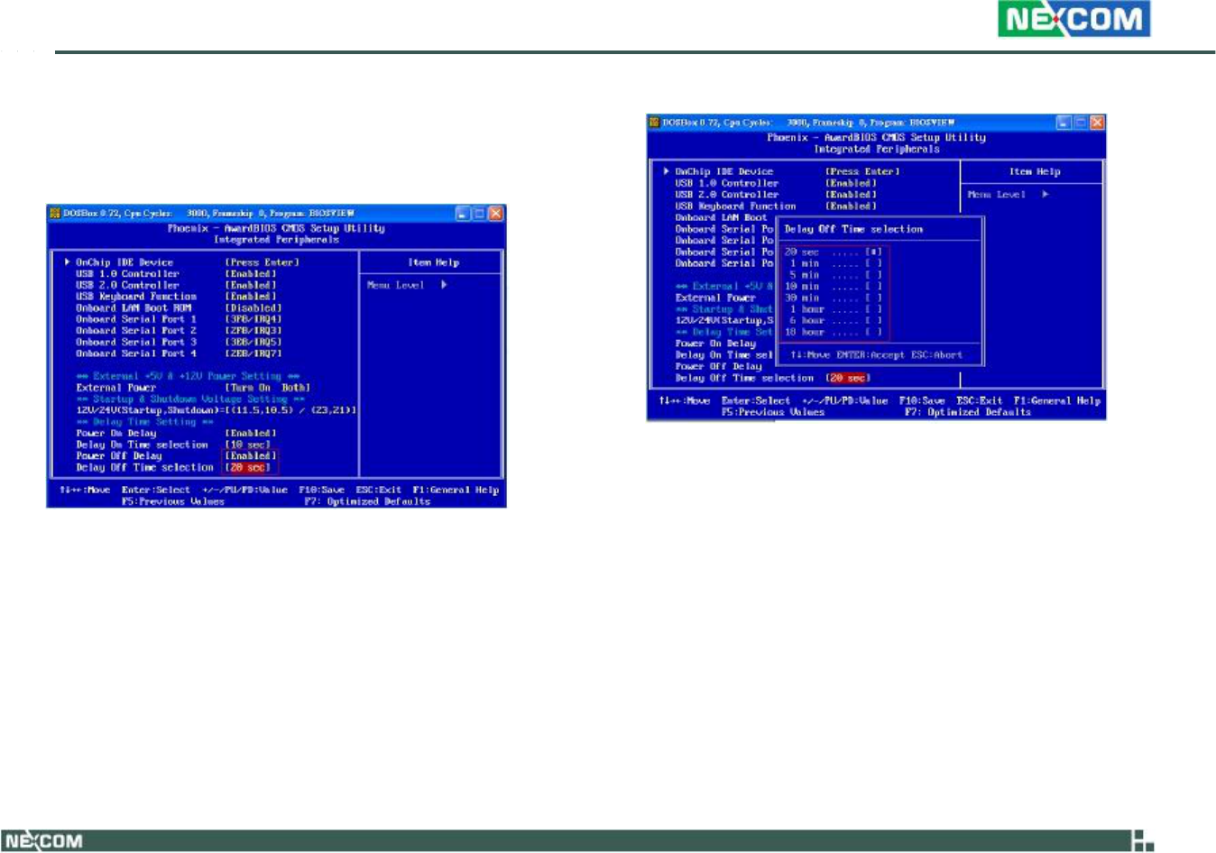
Appendix D: BIOS Setup
Enable
Power-off
Delay
Delay time can be set at 20sec/1min./5min./10min./30min./1hour/6hour/
18hour.
Copyright
©
2009
NEXCOM
International
Co.,
Ltd.
All
Rights
Reserved.
102
VTC
6110
User
Manual
Appendix E: Power Consumption
A
PPENDIX
E:
P
OWER
C
ONSUMPTION
OS:
XP English
Burn-in
Software:
Version 5.0
* Device: N/A
Copyright
©
2009
NEXCOM
International
Co.,
Ltd.
All
Rights
Reserved.
103
VTC
6110
User
Manual
Idle
Mode
100%
Burn-in
Mode
S3
S4
S5
1.47A / 12V
2.76A / 12V
0.11A / 12V
0.01A /12V
0.01A /12V
Federal Communications Commission (FCC) Statement
15.21
You are cautioned that changes or modifications not expressly approved by the part responsible for compliance could void the user’s authority to operate the
equipment.
15.105(b)
Federal Communications Commission (FCC) Statement
This equipment has been tested and found to comply with the limits for a Class B digital device, pursuant to part 15 of the FCC rules. These limits are designed to
provide reasonable protection against harmful interference in a residential installation. This equipment generates, uses and can radiate radio frequency energy and,
if not installed and used in accordance with the instructions, may cause harmful interference to radio communications. However, there is no guarantee that
interference will not occur in a particular installation. If this equipment does cause harmful interference to radio or television reception, which can be determined by
turning the equipment off and on, the user is encouraged to try to correct the interference by one or more of the following measures:
-Reorient or relocate the receiving antenna.
-Increase the separation between the equipment and receiver.
-Connect the equipment into an outlet on a circuit different from that to which the receiver is connected.
-Consult the dealer or an experienced radio/TV technician for help.
This device complies with Part 15 of the FCC Rules.Operation is subject to the following two conditions:
1) this device may not cause harmful interference and
2) this device must accept any interference received,, including interference that may cause undesired operation of the device.
FCC RF Radiation Exposure Statement:
1.This Transmitter must not be co-located or operating in conjunction with any other antenna or transmitter.
2.This equipment complies with FCC RF radiation exposure limits set forth for an uncontrolled environment. This equipment should be installed and operated
with a minimum distance of 20 centimeters between the radiator and your body.