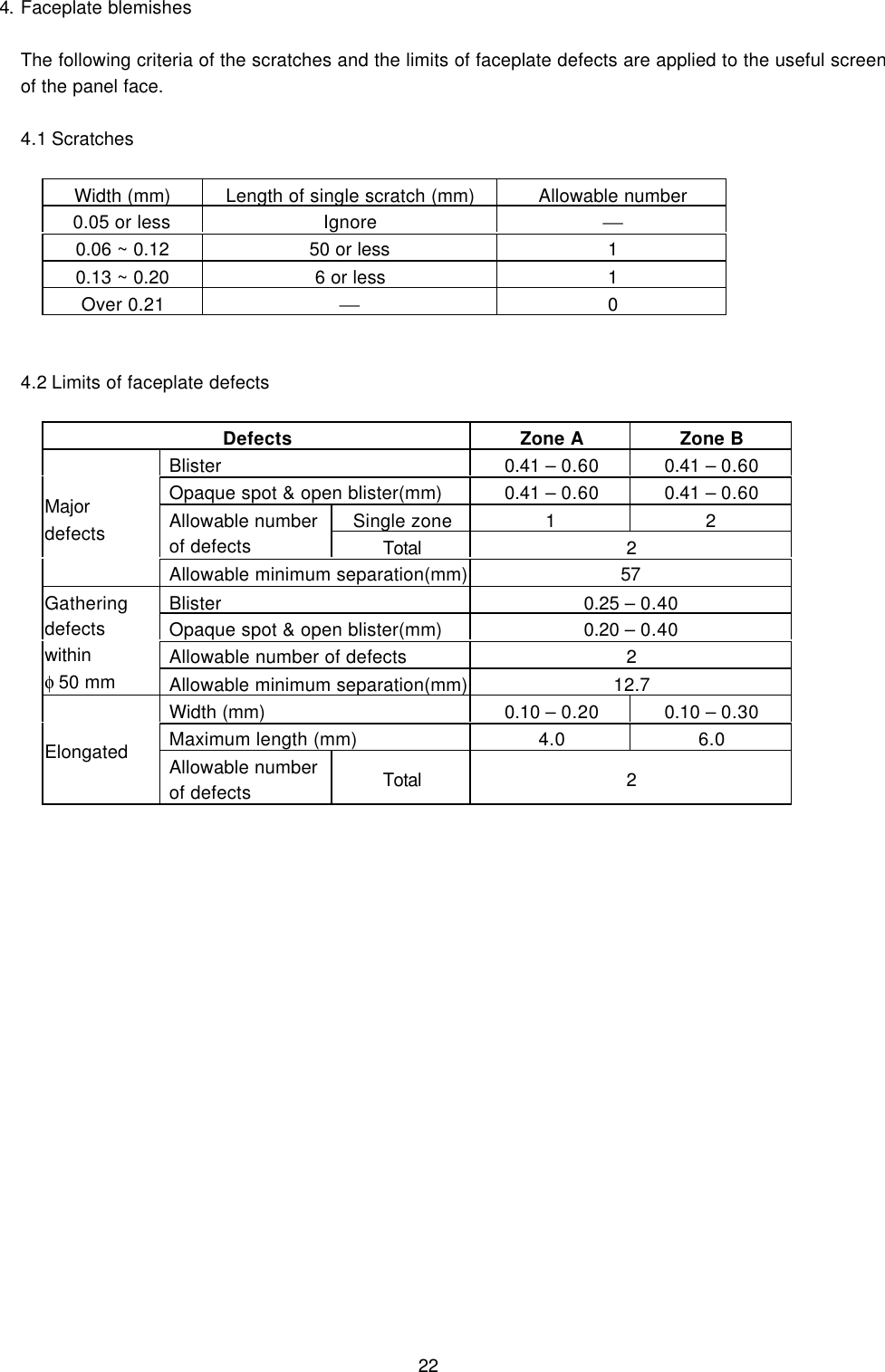
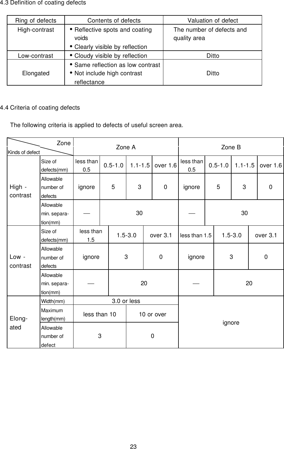
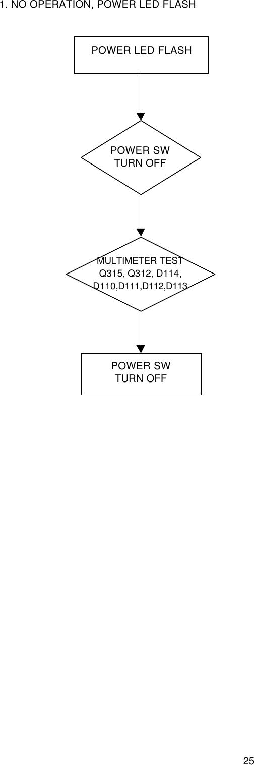
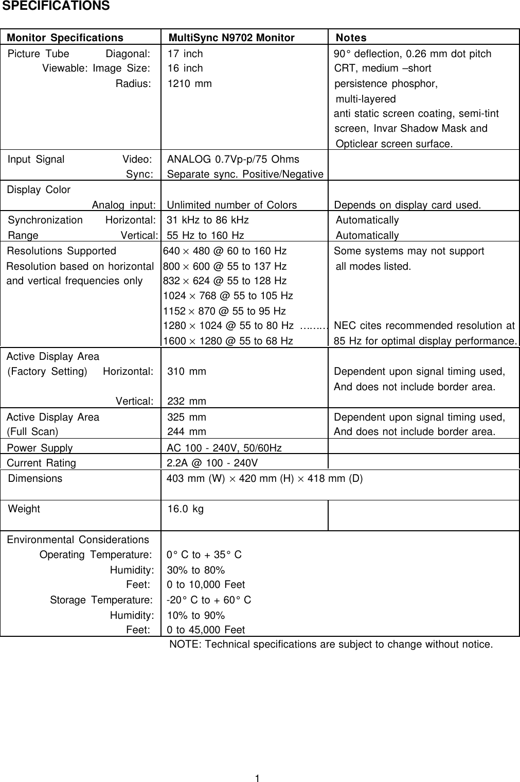
NPG Display Branch N9702 COLOR MONITOR User Manual N9702
NPG Display Ltd Taiwan Branch COLOR MONITOR N9702
UserManual.wiki
>
NPG Display Branch
>
N9702 User Manual
Exhibit 7
Navigation menu
Upload a User Manual
Namespaces
Wiki Guide
HTML
PDF
Info
Views
User Manual
Discussion / Help
Navigation
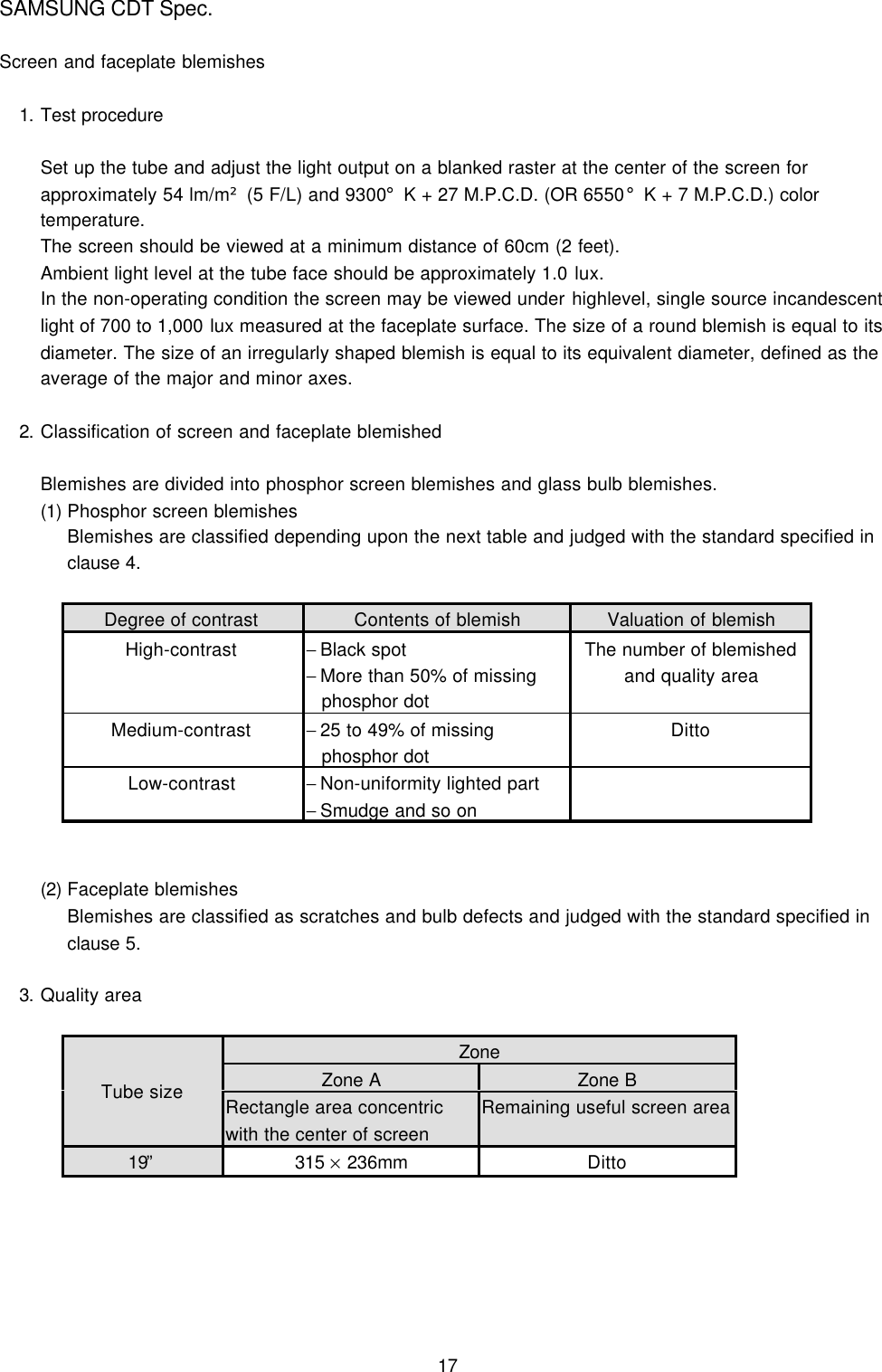
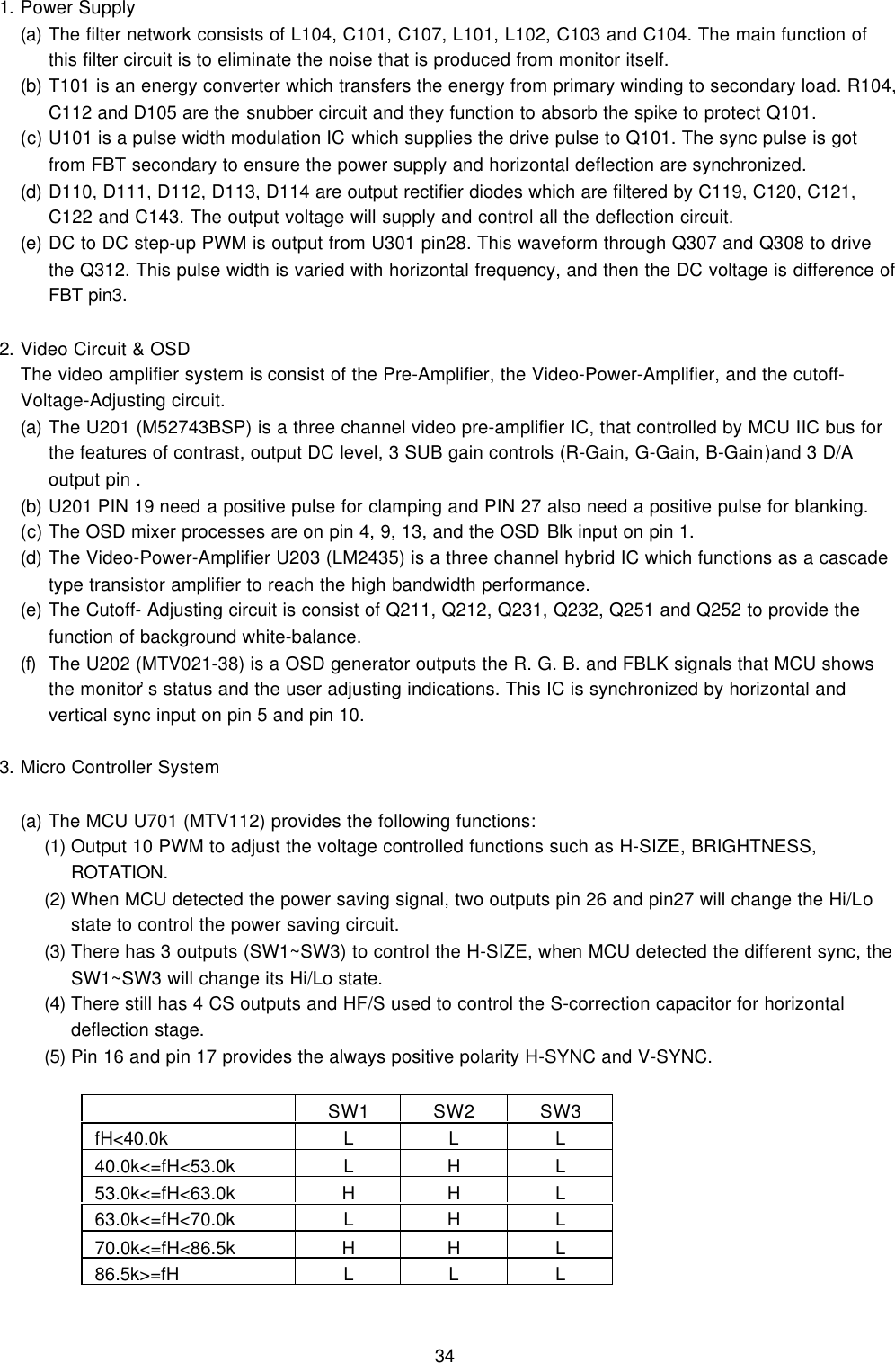
![213.2 High contrast blemishesAllowable number of blemishes Min. separation [mm]Blemish Zone A Zone B Total (zone A & B) Zone A Zone BA1 trio 111 B* (1) 000 * (2) 1 2 2 50 50C* (3) 1 2 2 50 20green 3 2blue 5 4D1 dotred 5 410 50 20EIncase of C+D 50 20*Note: (1) 3 or more consecutive same color phosphor dots(2) 2 consecutive same color phosphor dots(3) 2 consecutive different color phosphor dots3.3 Medium contrast blemishesAllowable max. number Allowable min. separation [mm]Blemish Zone A Zone B Zone A Zone B3 consecutive dots 1 2 -302 consecutive dots 3 6 30 201 dot ignore Ignore 3.4 Low contrast blemishesBlemishes in zone A Equivalent diameter of the total area of low-contrast blemishes should be less than 13mm.Extended blemishes inboth zone A and BEquivalent diameter of the total area of low-contrast blemishes should be less than 50mm.3.5 Other defectsEquivalent diameter of the total area should be less than 13mm.](https://usermanual.wiki/NPG-Display-Branch/N9702/User-Guide-87343-Page-21.png)