NPG Display Branch N9702 COLOR MONITOR User Manual N9702
NPG Display Ltd Taiwan Branch COLOR MONITOR N9702
Exhibit 7
1
SPECIFICATIONS
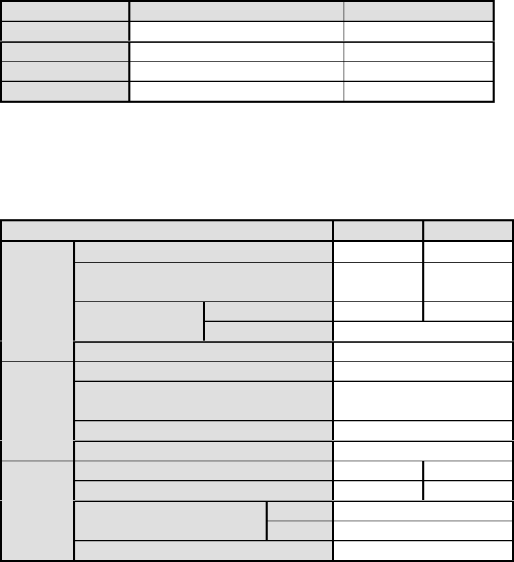
Monitor Specifications MultiSync N9702 Monitor Notes
Picture Tube Diagonal:
Viewable: Image Size:
Radius:
17 inch
16 inch
1210 mm
90° deflection, 0.26 mm dot pitch
CRT, medium –short
persistence phosphor,
multi-layered
anti static screen coating, semi-tint
screen, Invar Shadow Mask and
Opticlear screen surface.
Input Signal Video:
Sync:
ANALOG 0.7Vp-p/75 Ohms
Separate sync. Positive/Negative
Display Color
Analog input:
Unlimited number of Colors
Depends on display card used.
Synchronization Horizontal:
Range Vertical:
31 kHz to 86 kHz
55 Hz to 160 Hz
Automatically
Automatically
Resolutions Supported
Resolution based on horizontal
and vertical frequencies only
640 × 480 @ 60 to 160 Hz
800 × 600 @ 55 to 137 Hz
832 × 624 @ 55 to 128 Hz
1024 × 768 @ 55 to 105 Hz
1152 × 870 @ 55 to 95 Hz
1280 × 1024 @ 55 to 80 Hz ………
1600 × 1280 @ 55 to 68 Hz
Some systems may not support
all modes listed.
NEC cites recommended resolution at
85 Hz for optimal display performance.
Active Display Area
(Factory Setting) Horizontal:
Vertical:
310 mm
232 mm
Dependent upon signal timing used,
And does not include border area.
Active Display Area
(Full Scan)
325 mm
244 mm
Dependent upon signal timing used,
And does not include border area.
Power Supply AC 100 - 240V, 50/60Hz
Current Rating 2.2A @ 100 - 240V
Dimensions 403 mm (W) × 420 mm (H) × 418 mm (D)
Weight 16.0 kg
Environmental Considerations
Operating Temperature:
Humidity:
Feet:
Storage Temperature:
Humidity:
Feet:
0° C to + 35° C
30% to 80%
0 to 10,000 Feet
-20° C to + 60° C
10% to 90%
0 to 45,000 Feet
NOTE: Technical specifications are subject to change without notice.
2
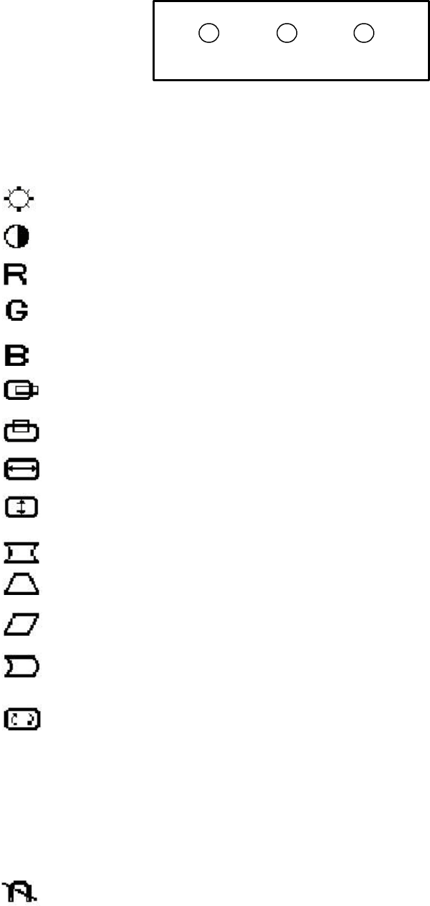
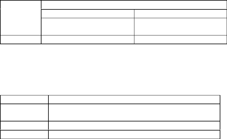
CONTROLS
On-screen display control buttons on the front of the monitor function as follows:
SELECT Enters and exits the OSM menu and decides the icon.
CONTROL
−
/
+Selects one of the controls and increases or decreases the adjustment.
RESET Resets the highlighted control to the factory Setting.
Adjusts the overall image and background screen brightness.
Adjusts the image brightness in relation to the background.
Red Color Control: Adjust the red contrast of the display.
Green Color Control: Adjust the green contrast of the display.
Blue Color Control: Adjust the blue contrast of the display.
Moves the image horizontally (left or right).
Moves the image vertically (up or down).
Increases or decreases the horizontal size of the image.
Increases or decreases the vertical size of the image.
Increases or decreases the curvature of the sides either inward or outward.
Increases or decreases the top of the screen to be the same as the bottom.
Increases or decreases the tilt of the sides either to the left or right.
Increases or decreases the curvature of the sides either to the left or right.
Rotates the entire display clockwise or counterclockwise.
Degauss Control: Eliminates the buildup of stray magnetic fields that alter the correct
scan of the electron beams and affect the purity of the screen colors, focus and
convergence. When activated, your screen image will jump and waver a bit as the screen is
+
–
SELECT RESET

3
demagnetized.
Caution: Please allows a minimum of 20 minutes to elapse
between uses of the Degauss Control.
9300K This color setting is adjusted at the factory to the stated Kelvin
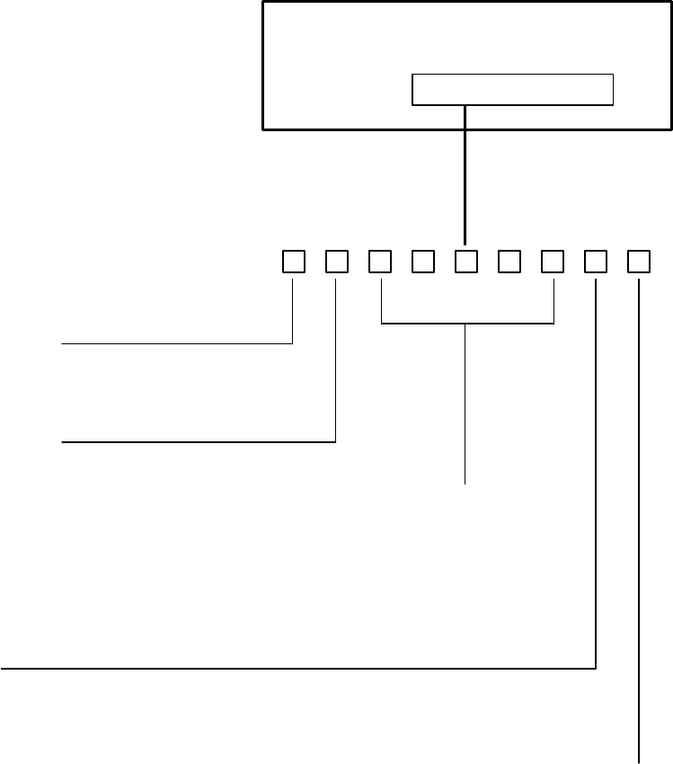
Moves the OSM menu vertically (up or down).
Moves the OSM menu horizontally (left or right).
EXIT: To exit the OSM window. Select EXIT in “Icon select window”, then push SELECT
button to exit OSM window.
Note: If no buttons are pushed after 10 seconds while in OSM, the window will
automactically disappear.
4
SERIAL NUMBER INFORMATION
Refer to the serial number information shown below.
SERIAL NUMBER LABEL
Manufactured Year :
( Last digit )
Manufactured Month :
January to September 1 to 9
October X
November Y
December Z
Factory mark :
NPG CHINA ...............................Y
It doesn’t have meaning specially
MODEL SERIAL No.
00001 ~ on ward
(Start from 00001 ~ when
month is changed.)
5
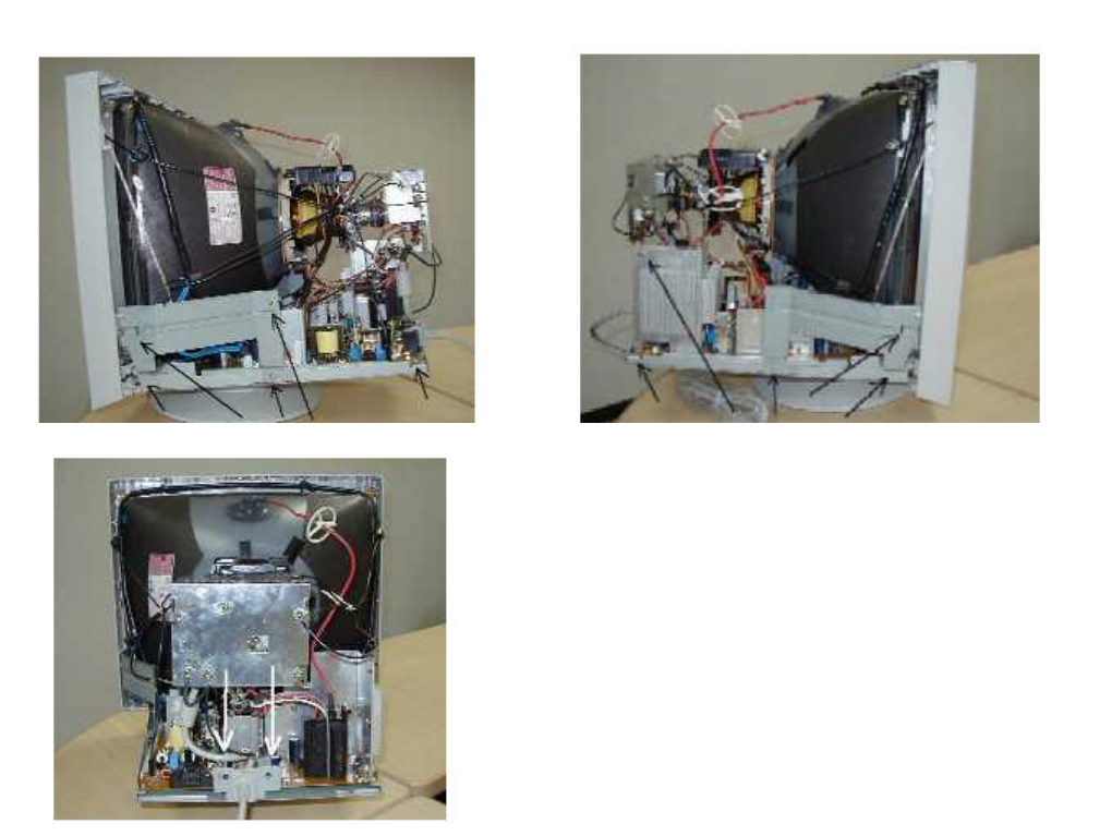
DISASSEMBLY
Ÿ Before you disassemble the set, turn off power and pull out the power plug.
Ÿ Use a proper screwdriver. If you user screwdriver that does not fit, you may damage the screws.
Ÿ Disassembly is the opposite process of assembly.
Ÿ Carefully discharge the CRT anode potential by grounding to CRT dag ground harness before
removing Anode Cap.
MAIN BOARD and CRT BOARD
EXPLANATION
1. Disassemble a screw like a picture.
2. Unsolder the GND wire (CRT coating earth wire) from MAIN BOARD ASSY and CRT BOARD ASSY.
This model has two kinds of CRT. Depend on CRT, the GND wire assembly is some different. Be
careful.
3. Disconnect the connector “S201”, “S202”, “S203”, Coating earth connector, and screen lead from the
CRT BOARD ASSY.
4. Disconnect the CRT BOARD ASSY from the CRT.
5. Disconnect the connector “S301”, “S601”, “S703”, “S701”, “S104” and “P102” from the MAIN BOARD
ASSY.
6. Remove the Anode Cap from the CRT.
NOTE: Carefully discharge the CRT anode by shorting it to ground before removing Anode Cap.
6
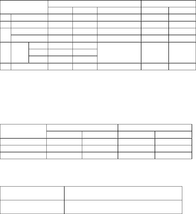
ADJUSTMENT SPECIFICATIONS
TABLE OF CONTENTS
Page
(1) Adjustment Tools ..................................................................................................................... 7
(2) Timing Table ........................................................................................................................... 7
(3) Definition for Normal Condition ................................................................................................. 7
(4) B+ Adjustment ........................................................................................................................ 7
(5) H. V. Adjustment ..................................................................................................................... 8
(6) X-ray Test ............................................................................................................................... 8
(7) H-Center Adjustment ............................................................................................................... 8
(8) H-Size Adjustment .................................................................................................................. 8
(9) Mode 11 Pre-Adjustment ......................................................................................................... 8
(10) White Balance Adjustment ..................................................................................................... 8
(11) Focus Adjust ......................................................................................................................... 8
(12) Convergence Adjust .............................................................................................................. 9
(13) Automatically adjust .............................................................................................................. 9
(14) White balance check and ABL adjust ...................................................................................... 9
(15) Power Saving Test ................................................................................................................ 9
(16) DCC 1/2B Test ...................................................................................................................... 10
(17) Timing Sheet ......................................................................................................................... 11
7
N9702 Adjustment Specifications Ver. 1.0
2000,1,06
(1) Adjustment tools:
(A) Color Analyzer (B) CHAROMA 2135 or Function Generator
(C) Multi meter (D) Hi-Pot Probe
(E) Convergence Meter (F) Degauss Probe
(G) Power Meter (H) Automatic Alignment System
(I) DDC test fixture
(2) TIMING TABLE(FACTORY MODE –16 MODES)
MODE RESOLUTION H-SYNC EREQ. V-SYNC FREQ H . POLARITY V . POLARITY
1VGA400 31.4kHz 70Hz -+
2VGA640*480 31.4kHz 60Hz - -
3640*480(75) 37.5kHz 75Hz - -
4640*480(85) 43.2kHz 85Hz - -
5800*600(75) 46.8kHz 75Hz + +
6MACⅡ 50K 49.7kHz 75Hz - -
7800*600(85) 53.6kHz 85Hz + +
81024*768(75) 60.0kHz 75Hz + +
91280*1024(60) 64.0kHz 60Hz + +
10 1024*768(85) 68.6kHz 85Hz + +
11 1280*1024(75) 79.9kHz 75Hz + +
12 Free run Adj. 30.0kHz 69Hz -+
13 H.CENTERING,EHT 85.938kHz 85Hz -+
(3) Definition for Normal Condition:
(A) INPUT AC VOLTAGE 110V/50HZ.
(B) WARM UP TIME 30 MINUTES.
(C) CROSSHATCH PATTERN.
(D) ALL VR ADJ CENTER.
(E) CRT FACE TO EAST DIRECTION
(F) COLOR TEMP 9300K
(4) B+ Adjustment:
(A) MODE: 69kHz 1024*768(85)
(B) PATTERN: CROSSHATCH
(C) Adjustment: Adjust VR102 to make the cathode of D112 has 14.8V±0.1V on cathode.
(D) CHECK: CHECK OTHER POWER SOURCE should be 82±2V,7.0±0.3V,
46V±2V,-12.1V±0.5V.
8
(5) H.V. Adjustment:
(A) MODE: 86kHz 85Hz
(B) PATTERN: ALL BLACK(Brightness cut off)
(C) Adjustment: Adjust VR302 to make the high voltage has 25.5±0.2KV
(6) H-Free run Adjustment:
(A) MODE: 30kHz
(B) PATTERN: ALL WHITE
(C) Adjustment: a. Tp6 connect 1uF/50V E-Cap to Ground.
b. Adjust VR306 to take H o/p Frequency is 30kHz or the screen stand up.
c. Take away E-Cap.
(7) X-RAY test:
(A) MODE: 86kHz 85Hz
(B) PATTERN: CROSSHATCH(Brightness just cut off)
(C) Test: a. Make TP1 and TP2 to be short circuit confirm the X-ray reactive.
b. Reset the power.
(8) H-CENTER adjustment
(A) MODE: 86kHz 85Hz
(B) PATTERN: CROSSHATCH
(C) Adjustment: Adjust VR301 to make raster is centrally on CRT
(9) H-size adjustment:
(A) MODE: 37.5kHz 640*480(75)
(B) PATTERN: CROSSHATCH
(C) Adjust H-SIZE, OSD set to Max, then adjust VR305 to make the full scan.
(10) MODE 11 Pre-Adjustment:
(A) MODE: 79.9kHz 1280*1024(75)
(B) PATTERN: CROSSHATCH
(C) Adjust V-CENTER, H-SIZE, V-SIZE, PINCUSHION, TRAPEZOID, H-PHASE to make Picture
Position Center and Picture Size 310*232mm.
(11) WHITE BALANCE adjustment
(A) MODE: 69kHz 1024*768(85)
(B) PATTERN: ALL BLACK
(C) Adjustment: a. WARM UP 30 min.
b. Make External Degauss.
c. Factory mode R-BIAS/G-BIAS/B-BIAS set to 20% data.
d. Adjust SCREEN VR (FBT) to 500±10V
e. CUT OFF Adjustment: Video signal off (0Vp-p), bright set to MAX, adjust
VR304 VR (G1), at the brightness 1~1.5FL.(4.2±0.8 cd/m²)
f. Adjust R-BIAS, G-BIAS, B-BIAS to make x=283±5, y=297±5, with
readjusting G2 to keep the brightness between 1~1.5FL(4.2±0.8 cd/m²).
9
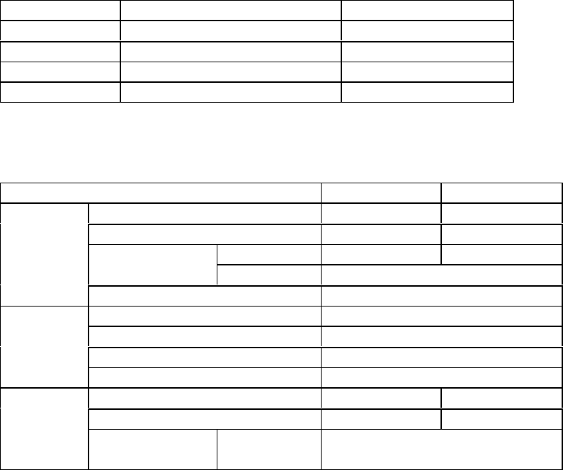
(12) FOCUS adjust:
(A) MODE: 86k 1280*960(85) ALL WHITE
(B) Adjust H.parabola Vp-p by OSM H-Focus control to keep P303 pin1 300Vp-p
(C) MODE: 46.875kHz 800*600(75) ALL WHITE
(D) Adjust H.parabola Vp-p same (B)
(E) MODE: 69kHz 1024*768(85)
(F) PATTERN: CROSSHATCH
(G) Adjust Focus VR(S), horizontal line must be clearly.
Adjust Focus VR(D), vertical line must be clearly.
(13) Convergence adjust:
(A) MODE: 69kHz 1024*768(85)
(B) PATTERN: CROSSHATCH.
(C) Adjustment: Use the convergence meter to check the spec. if can not follow the spec, adjust
Yoke coil to make be follow the spec.
(14) Automatically adjust:
Adjust H-SIZE, V-SIZE, H-PHASE, V-PHASE, PINCUSHION, TRAPEZOID R.G.B. GAIN by
factory product line automatic adjustment system─systemER9300 ,ER2300)(Adjust
NO.1~11MODE).
H.SIZE : 310±3mm
V.SIZE : 232±2mm
H.POSI : ±2mm
V.POSI : ±2mm
(15) White balance check and ABL adjust:
(A) MODE: 69kHz 1024*768(85)
(B) PATTERN: CENTER BLOCK(WINDOW)
(C) Contrast control set to Max and brightness control set to the Max, adjust R.G.B. GAIN
standard as below
9300K x=0.283±0.010 7500K x=0.300+0.010
y=0.297±0.010 y=0.315-0.010
Y=206±10 cd/m² Y=206+10 cd/m
6500K x=0.315±0.010
y=0.325±0.010
Y=206±10 cd/m²
(D) PATTERN: FULL WHITE 9300K.
(E) If they are out of spec, adjust to following:
BRIGHTNESS: Back raster is 0.2 cd/m² position
CONTRAST MAX: (MAX-5 digit )~(MAX)
Adjust R/G/B gain to be 9300K color due to about spec.
(F) When adjust 7500/6500K color,keep brightness and contrast max position to (E) condition.
Adjust R/G/B/ GAIN to be 7500/6500K color due to about spec..
(G) Adjustment: Brightness control and contrast control set to Max, adjust VR303 to Y=29~31FT-
L(103±3cd/m²)
10
(16) POWER SAVING Test:
(A) MODE: 60kHz 1024*768(75)
(B) PATTERN: ANY PATTERN.
(C) Adjustment:
a. It should be into suspend mode when signal quit after 5 sec.2nd the power output must be
≦15W. Check the LED color :Orange.
b. It should be into power off mode when into suspend mode after 3sec.and the power
output must be≦8W. Check the LED color :Orange
c. Transfer the signal and check the screen is normal. Check the LED color :Green
(17) DDC 1/2B Test:
(A) MODE: Any MODE.
(B) PATTERN: Any PATTERN.
(C) Scan bar code label and apply serial NO. to EDID Data.
11
(18) TIMING TABLE
Preset Mode No.
123456
VGA VGA VESA VESA VESA (MAC)
Signal Name 640*400 640*480 640*480 640*480 800*600 832*624
(75) (85) (75) (75)
Resolution
640*400 640*480 640*480 640*480 800*600 832*624
Dot Clock (MH 25.175 25.175 31.500 36.000 49.500 57.283
fh (kHz 31.47 31.469 37.50 43.269 46.875 49.725
fv (Hz) 70.09 59.940 75.00 85.008 75.00 74.550
Total
(dot)
800 800 840 832 1056 1152
(uS) 31.78 31.778 26.667 23.111 21.333 20.111
Disp (dot) 640 640 640 640 800 832
(uS) 25.42 25.422 20.317 17.778 16.162 14.523
Front (dot) 16 16 16 56 16 32
(uS) 0.64 0.636 0.508 1.556 0.323 0.559
Sync Pulse (dot) 96 96 64 56 80 64
(uS) 3.18 3.813 2.032 1.556 1.616 1.117
Back (dot) 48 48 120 80 160 224
(uS) 1.91 1.907 3.810 2.222 3.232 3.910
Total
(H)
449 525 500 509 625 667
(mS) 14.268 16.683 13.333 11.764 13.333 13.414
Disp (H) 400 480 480 480 600 624
(mS) 12.711 15.253 12.800 11.093 12.800 12.549
Front (H) 12 10 1 1 1 1
(mS) 0.381 0.318 0.027 0.023 0.021 0.020
Sync Pulse (H) 223333
(mS) 0.064 0.064 0.080 0.069 0.064 0.060
Back (H) 35 33 16 25 21 39
(mS) 1.112 1.049 0.427 0.578 0.448 0.784
Interlace
NON NON NON NON NON NON
Polarity (H/V NEG/POS NEG/NEG NEG/NEG NEG/NEG POS/POS NEG/NEG
Composite Sync
Composite Video
Character Font 7*9 7*9 7*9 7*9 7*9 7*9
Serration OFF OFF OFF OFF OFF OFF
EQP OFF OFF OFF OFF OFF OFF
12
Preset Mode No.
78910 11
VESA VESA VESA VESA VESA
Signal Name 800*600 1024*768 1280*1024 1024*768 1280*1024
(85) (75) (60) (85) (75)
Resolution
800*600 1024*768 1280*1024 1024*768 1280*1024
Dot Clock (MHz) 56.250 78.750 108.000 94.5 135.0
fh (kHz) 53.674 60.023 63.981 68.677 79.976
fv (Hz) 85.061 75.029 60.020 85 75.025
Total
(dot)
1048 1312 1688 1376 1688
(uS) 18.631 16.660 15.630 14.561 12.504
Disp (dot) 800 1024 1280 1024 1280
(uS) 14.222 13.003 11.852 10.836 9.481
Front (dot) 32 16 48 48 16
(uS) 0.569 0.203 0.444 0.508 0.119
Sync (dot) 64 96 112 96 144
(uS) 1.138 1.219 1.037 1.016 1.067
Back (dot) 152 176 248 208 248
(uS) 2.702 2.235 2.296 2.201 1.873
Total
(H)
631 800 1066 808 1066
(mS) 11.756 13.328 16.661 11.765 13.329
Disp (H) 600 768 1024 768 1024
(mS) 11.179 12.795 16.005 11.183 12.804
Front (H) 11111
(mS) 0.019 0.017 0.016 0.015 0.013
Sync (H) 33333
(mS) 0.056 0.050 0.047 0.044 0.038
Back (H) 27 28 38 36 38
(mS) 0.503 0.466 0.594 0.524 0.475
Interlace
NON NON NON NON NON
Polarity (H/V) POS/POS POS/POS POS/POS POS/POS POS/POS
Composite Sync
Composite Video
Character Font 7*9 7*9 7*9 7*9 7*9
Serration OFF OFF OFF OFF OFF
EQP OFF OFF OFF OFF OFF
13
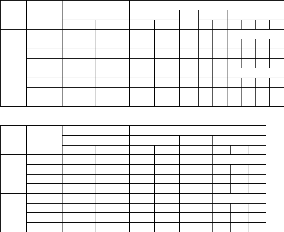
Preset Mode No.
15 16
Signal Name FREE H.CENT
Resolution
640*400 1024*768
Dot Clock (MHz) 25.24 125.4
fh (kHz) 30.05 85.938
fv (Hz) 69.56 85.002
Total
(dot)
840 1728
(uS) 33.278 11.636
Disp (dot) 640 1280
(uS) 25.357 8.62
Front (dot) 16 64
(uS) 0.631 0.431
Sync (dot) 64 160
(uS) 2.536 1.077
Back (dot) 120 224
(uS) 4.754 1.508
Total
(H)
432 1011
(mS) 14.376 11.764
Disp (H) 400 960
(mS) 13.311 11.171
Front (H) 1 1
(mS) 0.033 0.012
Sync (H) 2 3
(mS) 0.067 0.035
Back (H) 29 47
(mS) 0.956 0.547
Interlace
NON NON
Polarity (H/V) NEG/POS POS/POS
Composite Sync
Composite Video
Character Font 7*9 7*9
Serration OFF OFF
EQP OFF OFF
14
INSPECTION
1. Inspection of PLUG & PLAY communication
1-1. A construction of System
This system should be connected as shown below.
1-2. Starting method
1) Input Signal
Input signal must be separate sync. Timing is the signal whose vertical synchronization frequency is
between 55Hz and 25kHz.
Horizontal synchronization frequency should be set to 31.5kHz.
2) Power ON procedure
ž First, put the floppy disk for PnP Inspection into PC and turn on PC.
ž Turn on Fixture.
ž Make sure that fixture’s LED turns on and off.
ž Turn on signal generator and monitor.
3) Starting PC Software
ž Inspection of PnP communication
To check the PnP communication, for N9702, EDID file name is N9702.
Type “P N9702” on DOS command line and press return key.
ž Writing EDID to EEPROM and inspection of PnP communication
To write EDID to EEPROM and check the PnP communication of N9702, type “WP N9702”
on DOS prompt line and press return key.
Monitor
Fixture
Signal Cable
RGB H VPower Cable
Power Cable
Signal Generator
[
TEST PROGRAM
PART No. 599910408 Program Disk
PC
15
1-3. Operation
ž The operation should be performed according to the screen message.
ž The message of “Normally Complete” means that writing of EDID data or PnP inspection completed
normally.
The message of “Error” means that writing of EDID data or PnP inspection finished incorrectly.
ž When the PnP inspection is completed, read EDID data would be displayed. And if the read EDID
data differed from the original EDID data, the different bytes would be displayed in red.
ž For the details of error, see the messages displayed at the bottom right of the screen.
The meaning of the messages is shown on section 4.
ž After writing of EDID data or inspection of DDC2B, monitor can not be communicated by DDC1.
In that case, turn off and on the monitor again, which will make the DDC1 communication test
possible.
ž Make sure that fixture’s LED flashes on and off before writing EDID data, inspecting DDC1 and
DDC2B. If the fixture’s LED does not flash on and off, turn off and turn on the monitor and the fixture.
1-4. Error Messages
ž Start Bit Error
This message is displayed when the start bit is not “H” while sending data from PC to MPU on the
fixture. This error will be caused by noise etc. on the line.
ž Command Error
This message is displayed when the different command is sent from PC to MPU on the fixture.
ž Hardware Error
This message means that the PC does not recognize ACK command sent from the MPU on the
fixture.
ž File Open Error
This message means that the input EDID file name was wrong.
ž Command line Switch Error
This message means that the input communication command is incorrect.
ž Parity Error
This message is displayed when the MPU on the fixture recognized the parity bit is incorrect.
This error can be caused by noise etc. on the line.
ž EDID Data Error
This message is displayed when the null bit is not detected in EDID data read by DDC1
communication.
ž EDID Data Sort Error
This message is displayed when the header code is not detected in EDID data read by DDC1
communication.
ž Time Out Error
This message is displayed when the PC does not recognize ACK commands sent from MPU within
10 msec after the PC had sent communication command or EDID data.
If this error occurs, check the connection on PC, fixture and monitor.
16
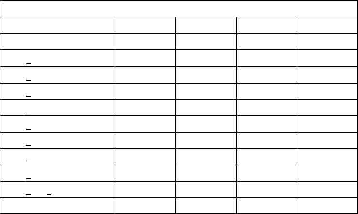
1-5. EDID data file
The EDID data file text is shown below. When you write or inspect EDID for this monitor, the following
table can be used.
File name: N9702
0123456789ABCDEF
00 00 FF FF FF FF FF FF 00 38 A3 F0 AB 01 01 01 01
10 *1) *2) 01 02 08 25 1B 78 EA 22 28 A1 54 48 99 26
20 11 48 4C FF FF 80 31 59 45 59 61 59 71 4F 81 59
30 81 99 A9 4F D1 40 86 3D 00 C0 51 00 30 40 40 A0
40 13 00 64 0B 11 00 00 1E 00 00 00 FD 00 37 A0 1F
50 60 18 00 0A 20 20 20 20 20 20 00 00 00 FC 00 4D
60 75 6C 74 69 53 79 6E 63 20 39 30 0A 00 00 00 FF
70 00 *3) *3) *3) *3) *3) *3) *3) *3) *3) *3) *3) *3) *3) 00 *4)
Table 1-1. Data list (Management number)
※1 : address 10h Month of Manufacture × 4
※2 : address 11h Year of Manufacture – 1990
※3 : address 71h ~7Dh Serial Number String (ASCII code) If less than 13 bytes then terminate
with ASCII code 0Ah and pad field with ASCII code 20h.
※4 : address 7h This Address should be programmed such that a one-byte checksum of
the entire 128 byte EDID equals 00h.
Diagram 1-1 Timing chart of DDC2B
CONTROL
BYTE
DATA n DATA n+ 1 DATA n+X
A
C
K
A
C
K
A
C
K
S
T
A
R
T
S
P
BUS ACTIVITY
MASTER
SDA LINE
12pin
BUS ACTIVITY
17
SAMSUNG CDT Spec.
Screen and faceplate blemishes
1. Test procedure
Set up the tube and adjust the light output on a blanked raster at the center of the screen for
approximately 54 lm/m² (5 F/L) and 9300°K + 27 M.P.C.D. (OR 6550°K + 7 M.P.C.D.) color
temperature.
The screen should be viewed at a minimum distance of 60cm (2 feet).
Ambient light level at the tube face should be approximately 1.0 lux.
In the non-operating condition the screen may be viewed under highlevel, single source incandescent
light of 700 to 1,000 lux measured at the faceplate surface. The size of a round blemish is equal to its
diameter. The size of an irregularly shaped blemish is equal to its equivalent diameter, defined as the
average of the major and minor axes.
2. Classification of screen and faceplate blemished
Blemishes are divided into phosphor screen blemishes and glass bulb blemishes.
(1) Phosphor screen blemishes
Blemishes are classified depending upon the next table and judged with the standard specified in
clause 4.
Degree of contrast Contents of blemish Valuation of blemish
High-contrast − Black spot
− More than 50% of missing
phosphor dot
The number of blemished
and quality area
Medium-contrast − 25 to 49% of missing
phosphor dot
Ditto
Low-contrast − Non-uniformity lighted part
− Smudge and so on
(2) Faceplate blemishes
Blemishes are classified as scratches and bulb defects and judged with the standard specified in
clause 5.
3. Quality area
Zone
Zone A Zone B
Tube size Rectangle area concentric
with the center of screen
Remaining useful screen area
19”315 × 236mm Ditto
18
4. Limits of phosphor screen blemishes
(1) High-contrast blemishes
The following criteria is applied to high-contrast blemishes.
Allowable No. of blemishes Allowable
Minimum
Separation(mm)
Blemish Zone A Zone B Total
(Zone A & B) Zone A Zone B A + B
A1 trio 1 1 2 ----- 20
B(1) 0 0 0
(2) 1 2 2 20 20C
(3) 1 2 2 ---- 20 20
Green 3 4
Red 5 6D
1 dot
Blue 5 6
10 50 20 20
EIn case of
A+C
50 20 20
FIn case of
A+C+D
50 20 20
(1) 3 or more consecutive same color phosphor dots
(2) 2 consecutive same color phosphor dots
(3) 2 consecutive different color phosphor dots
(2) Medium-contrast blemishes
The following criteria is applied to medium-contrast blemishes.
Allowable maximum
number
Allowable minimum
separation(mm)Blemish
Zone A Zone B Zone A Zone A+B
3 consecutive dot 2 4 30 30
2 consecutive dot 3 7 20 20
1 dot ignore ignore
Note) Minimum separation is 20 mm among any high and medium contrast blemishes
(excluding 1 dot medium contrast blemishes).
(3) Low-contrast blemishes
The following criteria is applied to low-contrast blemishes.
Blemishes
In zone A
Equivalent diameter of the total area of low-
contrast blemishes should be less than 13mm.
Extended blemishes
In both zones A and B
Equivalent diameter of the total area of low-
contrast blemishes should be less than 50mm.
19
5. Limits of faceplate blemishes
(1) Scratches
The following criteria is applied to scratches on the faceplate of color display tubes.
Maximum size of scratches allowable
Width (mm) Length of single scratch(mm) Allowable number
0.05 or less Ignore
0.06 ~ 0.12 50 or less 1
0.13 ~ 0.20 10 or less 1
Over 0.20 0
(2) Limits of faceplate defects
The following criteria is applied to defects of useful screen on panel face.
Zone Zone A Zone B
Blister (mm) 0.41 ~ 0.60 0.41 ~ 0.60
Opaque spot &
open blister (mm)
0.31 ~ 0.50 0.31 ~ 0.50
Single zone 1 2Allowable number
of defects Total 3
Major
defects
Allowable minimum separation(mm) 50
Blister (mm) 0.25 ~ 0.60
Opaque spot &
open blister (mm)
0.20 ~ 0.60
Allowable number of defects 4
Gathering
defects
within
ϕ
50mm Allowable minimum separation 12.7
Width (mm) 0.10 ~ 0.20 0.10 ~ 0.30
Maximum length (mm) 4.0 6.0
Single 2Allowable number of defects
Total 2
Elongated
Allowable minimum separation 76
20
LG CDT Spec.
Limits of Screen and Faceplate Blemish
1. Test Procedure
Set up the tube and adjust the light output on a blank raster at the center of the screen for
approximately 15 FL and C.I.E x = 0.281, y = 0.311 (or x = 0.313, y = 0.329) color coordinate.
The screen should be viewed at the minimum distance of 60 cm (2 feet).
Ambient light level at the tube face should be approximately 5.0 Lux.
In the non-operating condition the screen may be viewed under high level, single-source incandescent
light of 700 to 1,000 lux measured at the faceplate surface.
The size of a round blemish is equal to its diameter. The size of an irregularly shaped blemish is equal
to its equivalent diameter, defined as the average of the major and minor axis.
2. Quality area
Zone
Zone A Zone B
Tube size Rectangle area concentric
with the center of screen
Remained useful screen area
41 cm 300mm x 225mm Remained area
3. Phosphor screen blemishes
3.1 The criteria of blemish classification
Category Contents of blemish
Entire defects Blank Spot
50% or more of complete dot is missing
Partial defects 25 to 49% of complete dot is missing
Other defects Non-uniformity lighted part
21
3.2 High contrast blemishes
Allowable number of blemishes Min. separation [mm]
Blemish Zone A Zone B Total (zone A & B) Zone A Zone B
A1 trio 111
B* (1) 000
* (2) 1 2 2 50 50
C* (3) 1 2 2 50 20
green 3 2
blue 5 4
D1 dot
red 5 4
10 50 20
EIncase of C+D 50 20
*Note: (1) 3 or more consecutive same color phosphor dots
(2) 2 consecutive same color phosphor dots
(3) 2 consecutive different color phosphor dots
3.3 Medium contrast blemishes
Allowable max. number Allowable min. separation [mm]
Blemish Zone A Zone B Zone A Zone B
3 consecutive dots 1 2 -30
2 consecutive dots 3 6 30 20
1 dot ignore Ignore
3.4 Low contrast blemishes
Blemishes in zone A Equivalent diameter of the total area of low-
contrast blemishes should be less than 13mm.
Extended blemishes in
both zone A and B
Equivalent diameter of the total area of low-
contrast blemishes should be less than 50mm.
3.5 Other defects
Equivalent diameter of the total area should be less than 13mm.
22
4. Faceplate blemishes
The following criteria of the scratches and the limits of faceplate defects are applied to the useful screen
of the panel face.
4.1 Scratches
Width (mm) Length of single scratch (mm) Allowable number
0.05 or less Ignore
0.06 ~ 0.12 50 or less 1
0.13 ~ 0.20 6 or less 1
Over 0.21 0
4.2 Limits of faceplate defects
Defects Zone A Zone B
Blister 0.41 – 0.60 0.41 – 0.60
Opaque spot & open blister(mm) 0.41 – 0.60 0.41 – 0.60
Single zone 1 2Allowable number
of defects Total 2
Major
defects
Allowable minimum separation(mm) 57
Blister 0.25 – 0.40
Opaque spot & open blister(mm) 0.20 – 0.40
Allowable number of defects 2
Gathering
defects
within
φ 50 mm Allowable minimum separation(mm) 12.7
Width (mm) 0.10 – 0.20 0.10 – 0.30
Maximum length (mm) 4.0 6.0
Elongated Allowable number
of defects Total 2
23
4.3 Definition of coating defects
Ring of defects Contents of defects Valuation of defect
High-contrast Ÿ Reflective spots and coating
voids
Ÿ Clearly visible by reflection
The number of defects and
quality area
Low-contrast Ÿ Cloudy visible by reflection Ditto
Elongated
Ÿ Same reflection as low contrast
Ÿ Not include high contrast
reflectance
Ditto
4.4 Criteria of coating defects
The following criteria is applied to defects of useful screen area.
Zone
Kinds of defect Zone A Zone B
Size of
defects(mm)
less than
0.5 0.5-1.0 1.1-1.5 over 1.6 less than
0.5 0.5-1.0 1.1-1.5 over 1.6
Allowable
number of
defects
ignore 5 3 0 ignore 5 3 0High -
contrast
Allowable
min. separa-
tion(mm)
30 30
Size of
defects(mm)
less than
1.5 1.5-3.0 over 3.1 less than 1.5 1.5-3.0 over 3.1
Allowable
number of
defects
ignore 3 0 ignore 3 0Low -
contrast
Allowable
min. separa-
tion(mm)
20 20
Width(mm) 3.0 or less
Maximum
length(mm) less than 10 10 or over
Elong-
ated Allowable
number of
defect
3 0
ignore
24
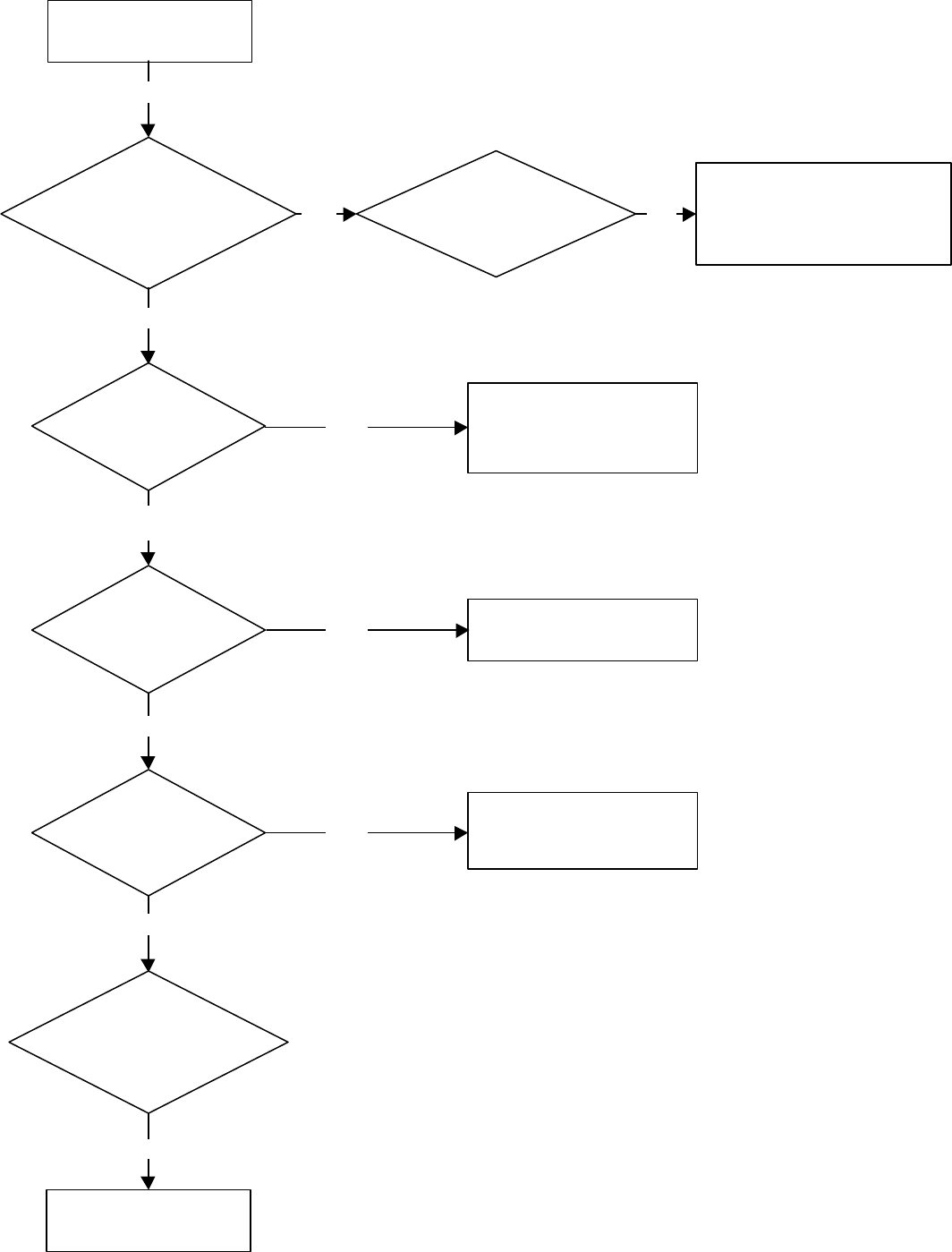
TROUBLE SHOOTING
Refer to User’s Manual trouble shooting section before using this chart.
TABLE OF CONTENTS
Page
1. NO OPERATION, POWER LED FLASH ...................................................................................... 25
2. NO OPERATION, POWER LED OFF .......................................................................................... 26
3. VIDEO NOISE, UNSYNCHRONOUS .......................................................................................... 27
4. NO VIDEO ................................................................................................................................. 28
5. NO RASTER .............................................................................................................................. 29
6. TROUBLE IN H.V SYNC ............................................................................................................ 30
7. PINCUSHION POOR ................................................................................................................. 31
8. FOCUS POOR ........................................................................................................................... 32
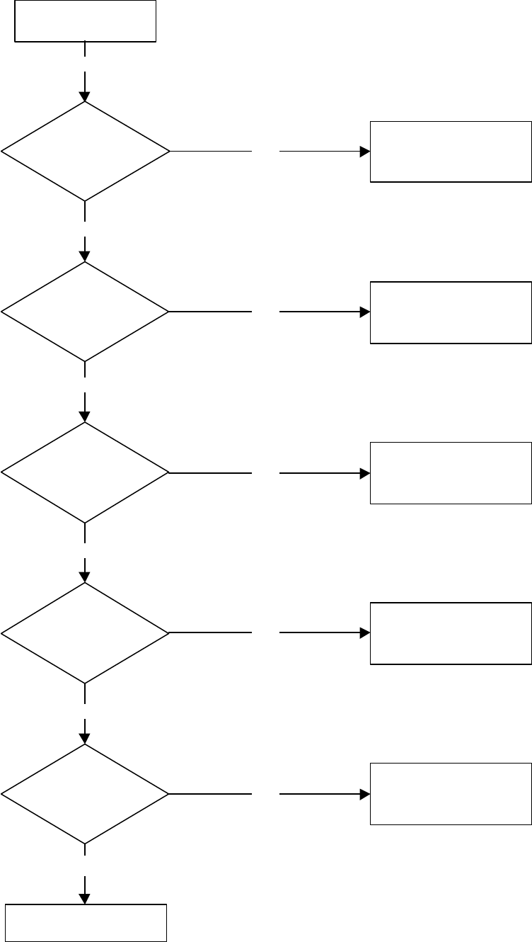
25
1. NO OPERATION, POWER LED FLASH
POWER LED FLASH
POWER SW
TURN OFF
POWER SW
TURN OFF
MULTIMETER TEST
Q315, Q312, D114,
D110,D111,D112,D113
26
2. NO OPERATION, POWER LED OFF
1. DC P/S O/P VOLTAGE SET AT 17V,CURRENT SET
AT 200MA. POSITIVE CONNECT TO C109”+”.
NEGATIVE CONNECT TO C105”-“.
2. SCOPE SET AT 10V/DIV, 10US/DIV, PROBE
CONNECT TO Q101-GATE AND C105”-“.
POWER SW
TURN OFF
CHECK
F101
CHECK
Q101
CHECK
U101
U101 PIN6
PULSE O/P
POWER SW
TURN ON FAILURE
R111, ZD103
CHECK
U101 PIN 7 VCC
PIN 4 SAWTOOTH
PIN 8 = 5V
NO
27
3. VIDEO NOISE, UNSYNCHRONOUS
CHECK HORIZONTAL
FREQUENCY C114 TO GND
CHECK
Q312 FREQUENCY
SYNCRONIZE
WITH H-SYNC
CHECK U301
NORMAL OPERATION
CHECK
Q101 G-S FREQUENCY
SYNCRONIZE
WITH H-SYNC
CHECK C114, R116
D109, R115, R117
YES
YES
NONO
NO
28
4. NO VIDEO
NO VIDEO
YES
CHECK
SCREEN CONTROL
CLOCKWISE
YES
CHECK
U201 PIN 2, 6, 11
SIGNAL LEVEL
YES
CHECK
U201 PIN 29, 32, 35
SIGNAL LEVEL
TROUBLE IN U201
CLAMP(PIN 19)
U201 12V VOLTAGE
YES
CHECK
U203 PIN 1, 2, 3
SIGNAL LEVEL
CHECK
CATHODE VIDEO
LEVEL
TROUBLE IN CRT
YES
YES
TROUBLE IN U203
R216, R236, R256
NO
TROUBLE IN U203
12V, 80V VOLTAGE
NO
NO
TROUBLE IN
R/G/B SIGNAL,
SIGNAL CABLE
NO
REFER
NO RASTER
NO
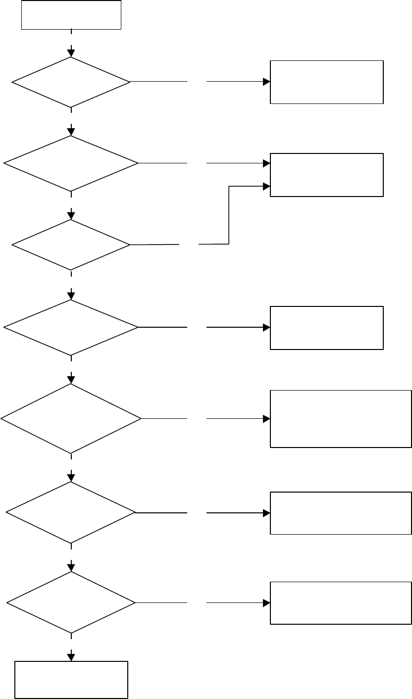
29
5. NO RASTER
CHECK
U301 PIN 1, PIN 2
H/V SYNC
NO RASTER
CHECK
B+
TROUBLE IN
MCU U701
YES
YES
TROUBLE IN
Q315,Q316,T301,D320,
D321,T302
CHECK Q315
COLLECTOR ABOUT
1050Vp-p
CHECK G1
VOLTAGE ABOUT
-45~65V
TROUBLE IN
G2 VOLTAGE
YES
YES
TROUBLE IN
Q323, Q331, R394, D314,
T302, C328, U701
NO
NO
CHECK
T302 PIN 3 VOLTAGE
62V AT 31.5KHz, 180V
AT 86KHz
TROUBLE IN
U301,Q312,D317,D111,R31A,
R384, Q307, Q308
OR DEFLECTION YOKE
YES
NO
CHECK
U301 PIN 26, 3
H/V SYNC
TROUBLE IN
U301
YES
YES
NO
NO
POWER SUPPLY
CHECK
NO
YES
CHECK
U701 PIN IS LOW
NO
30
6. TROUBLE IN H. V SYNC
TROUBLE IN
HOR. OR VER. SYNC
CHECK
CONNECTOR S701
(PIN6,7), SIGNAL
TROUBLE IN
SIGNAL CABLE
CHECK
U701(PIN 13,15)
H/V SYNC.
SIGNAL
TROUBLE IN
H/V SYNC LINE &
Q701, Q702
CHECK
U701(PIN 16,17)
H/V SYNC.
SIGNAL
CHECK
U701(PIN 40)
VOLTAGE
5V?
TROUBLE IN
5V LINE
YES
NO
YES
YES
YES
CHECK
U301(PIN 1, 2)
TROUBLE IN
U301
YES
YES
NO
NO
NO
CHECK
U701 (PIN 18, 19)
FREQ.8MHz
TROUBLE IN
H.V SIGNAL LINE
R301, R302, C301, C302
TROUBLE IN
X701, U701
NO
YES
NO
31
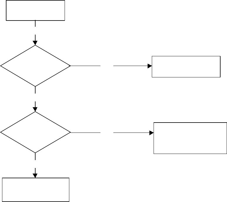
7. PINCUSHION POOR
PINCUSHION
POOR
PARABOLA
WAVE
CHECK
U301 PIN 24
PARABOLA
TROUBLE IN U301
CHECK C350, Q332,
Q314,Q342,R332, R330,
R32A,R32C,R30Y,32T
CHECK Q309, Q311,
Q332,Q341,Q342,C350
NO
NO
YES
YES
YES
32
8. FOCUS POOR
1. CHECK STATIC FOCUS AND
DYNAMIC FOCUS VR LINE TO
CRT SOCKET
2. CRT SOCKET OR CRT POOR
FOCUS POOR
CHECK
T302 12PIN H-DYNAMIC
PARABOLA WAVEFORM 500Vpp,
V-DYNAMIC PARABOLA
WAVEFORM 180Vpp
ADJUST
T302 STATIC FOCUS VR AND
DYNAMIC FOCUS VR
CHECK
T303 H AND V PARABOLA
WAVEFORM
CHECK
C323 H-PARABOLA
WAVEFORM 50Vpp
CHECK
U301 10PIN FOCUS; Q302
BASE H-PARABOLA
4-Vpp
GO TO
FACTORY MODE,
CHOICE H-FOCUS ICON, ADJUST
TO 70~100%, CHECK U301
10PIN FOCUS 4Vpp
TROUBLE IN U301
TROUBLE IN
T303, Q305, R360, R359,
R331, R32G, R329, R330,
R332,R32H,C320,C324,
TROUBLE IN T801
TROUBLE IN
Q302, Q338, Q304, Q303
R327, R363, R326
YES
YES NO
NO
YES
YES
NO
NO
NO
NO
H-PARABOLA
V-PARABOLA
NO
33
N9702 Theory of circuit operation
This monitor contains the following blocks
Page
1. Power Supply ............................................................................................................................34
2. Video Circuit & OSD ...................................................................................................................34
3. Micro Controller System .............................................................................................................34
4. Vertical Deflection ......................................................................................................................35
5. Horizontal Deflection ..................................................................................................................35
6. FBT Secondary & Dynamic Focus ...............................................................................................36
34
1. Power Supply
(a) The filter network consists of L104, C101, C107, L101, L102, C103 and C104. The main function of
this filter circuit is to eliminate the noise that is produced from monitor itself.
(b) T101 is an energy converter which transfers the energy from primary winding to secondary load. R104,
C112 and D105 are the snubber circuit and they function to absorb the spike to protect Q101.
(c) U101 is a pulse width modulation IC which supplies the drive pulse to Q101. The sync pulse is got
from FBT secondary to ensure the power supply and horizontal deflection are synchronized.
(d) D110, D111, D112, D113, D114 are output rectifier diodes which are filtered by C119, C120, C121,
C122 and C143. The output voltage will supply and control all the deflection circuit.
(e) DC to DC step-up PWM is output from U301 pin28. This waveform through Q307 and Q308 to drive
the Q312. This pulse width is varied with horizontal frequency, and then the DC voltage is difference of
FBT pin3.
2. Video Circuit & OSD
The video amplifier system is consist of the Pre-Amplifier, the Video-Power-Amplifier, and the cutoff-
Voltage-Adjusting circuit.
(a) The U201 (M52743BSP) is a three channel video pre-amplifier IC, that controlled by MCU IIC bus for
the features of contrast, output DC level, 3 SUB gain controls (R-Gain, G-Gain, B-Gain)and 3 D/A
output pin .
(b) U201 PIN 19 need a positive pulse for clamping and PIN 27 also need a positive pulse for blanking.
(c) The OSD mixer processes are on pin 4, 9, 13, and the OSD Blk input on pin 1.
(d) The Video-Power-Amplifier U203 (LM2435) is a three channel hybrid IC which functions as a cascade
type transistor amplifier to reach the high bandwidth performance.
(e) The Cutoff- Adjusting circuit is consist of Q211, Q212, Q231, Q232, Q251 and Q252 to provide the
function of background white-balance.
(f) The U202 (MTV021-38) is a OSD generator outputs the R. G. B. and FBLK signals that MCU shows
the monitor’s status and the user adjusting indications. This IC is synchronized by horizontal and
vertical sync input on pin 5 and pin 10.
3. Micro Controller System
(a) The MCU U701 (MTV112) provides the following functions:
(1) Output 10 PWM to adjust the voltage controlled functions such as H-SIZE, BRIGHTNESS,
ROTATION.
(2) When MCU detected the power saving signal, two outputs pin 26 and pin27 will change the Hi/Lo
state to control the power saving circuit.
(3) There has 3 outputs (SW1~SW3) to control the H-SIZE, when MCU detected the different sync, the
SW1~SW3 will change its Hi/Lo state.
(4) There still has 4 CS outputs and HF/S used to control the S-correction capacitor for horizontal
deflection stage.
(5) Pin 16 and pin 17 provides the always positive polarity H-SYNC and V-SYNC.
SW1 SW2 SW3
fH<40.0k L L L
40.0k<=fH<53.0k LHL
53.0k<=fH<63.0k H H L
63.0k<=fH<70.0k LHL
70.0k<=fH<86.5k H H L
86.5k>=fH L L L
35
Input Output
Sync Sync PS CS
Mode State
HVHV
Mute
121234
ON Pulses Pulses Pulse Pulse LH H Depend on fH
Stand By No pulses Pulses L L HLHLLLL
Suspend Pulses No pulses L L HLHLLLL
User
PMS_OFF No pulses No pulses L L HLLLLLL
ON Pulses Pulses Pulses Pulses LH H Depend on fH
Stand By No pulses Pulses L L L H H LLLL
Suspend Pulses No pulses L L L H H LLLL
Factory
PMS_OFF No pulses No pulses L L L H H LLLL
Input Output
Sync Sync Rotation SW
Mode State
HVHVDAC 123
ON Pulses Pulses Pulse Pulse Adj. data Depend on fH
Stand By No pulses Pulses L L 107/255 HHH
Suspend Pulses No pulses L L 107/255 HHH
User
PMS_OFF No pulses No pulses L L 0/255 HHH
ON Pulses Pulses Pulses Pulses Adj. data Depend on fH
Stand By No pulses Pulses L L Adj. data HHH
Suspend Pulses No pulses L L Adj. data HHH
Factory
PMS_OFF No pulses No pulses L L Adj. data HHH
(b) The U702 is an EEPROM IC which stores the parameters of each mode and the user adjusting result
and also DDC data. It is controlled by IIC bus from MCU.
4. Vertical Deflection
(a) Vertical deflection Saw-tooth waveform is provided by U301, pin 23, and amplified by U401 TDA8172.
(b) A voltage multiplier connected to pin 3 and pin 6, consists of D402, C409 to avoid flyback scanning line
appeared during the vertical flyback period.
(c) U301 (TDA9111) pin 21 provides a DC level as a V-Position control voltage.
(d) U401 pin 5 is output to drive vertical yoke.
5. Horizontal Deflection
(a) U301 is a horizontal signal processing IC. Horizontal Driver signal is output from pin 26 of U301
TDA9111 and through Q333, Q334 to drive Q316 and T301.
(b) T301 is an on/off type driver transformer. It functions to convert primary energy to secondary, and drive
the horizontal output transistor Q315, R369 and C363 are the snubber.
(c) Horizontal linearity and Cs circuit:
(1) Horizontal linearity and Cs is changed by RL301,RL301 can change Horizontal
Tr(C337),Linear(L302) and Cs(C336).It control by HF/S from U701 pin 30
36
(2) C344 is the Cs capacitor, and Q324 controls C345, Q326 controls C347, Q325 controls C346, Q327
controls C348. The U701 pin 1, 2, 3, 4 controls the Q324, Q326, Q325 and Q327 respectively. So
different frequency has different combination to meet the requirement.
Cs Table By Frequency
CS1 CS2 CS3 CS4
fH < 30K 0 0 0 0
30K < fH < 34K 0 0 0 0
34K < fH < 37K 0 0 1 0
37K < fH < 46K 0 1 1 0
46K < fH < 53K 1 0 0 1
53K < fH < 63K 1 1 0 1
63K < fH < 68K 0 0 1 1
68K < fH < 75K 1 0 1 1
75K < fH < 85K 0 1 1 1
85K < fH < 86.5K 1 1 1 1
86.5K < fH 0 0 0 0
6. FBT Secondary & Dynamic Focus
(a) Focus and screen voltage are come from FBT bleeder.
(b) G1 bias is controlled through R399, R30F, VR304, R30B and Q323.
(c) Q309 is controlled by MCU pin 31 Mute2, and it will blank the picture during mode change.
(d) Q401 is the blanking buffer to G1 to blank the retrace line of picture.
(e) Q339, Q340, D302,ZD301,D326,R322 and R318 are the x-ray protection circuit. Once the HV rises
abnormally, U301 win shut down itself, all the horizontal deflection is stopped by then.
(f) Dynamic Focus:
(1) H-Focus: U301 pin 10 outputs a parabolic waveform and through Q302 into Q338 to get a reverse
amplified waveform. This waveform is through the SEPP Q303 and Q304, as a current gain then
input into T303.
(2) V-Focus: U401 pin 5 output waveform through R329, C322, R32G and C324 to get a parabolic
waveform. This waveform is amplified by Q305 and input into T303.
(3) H-Focus and V-Focus are into T303 to get a combined waveform that will input to FBT.
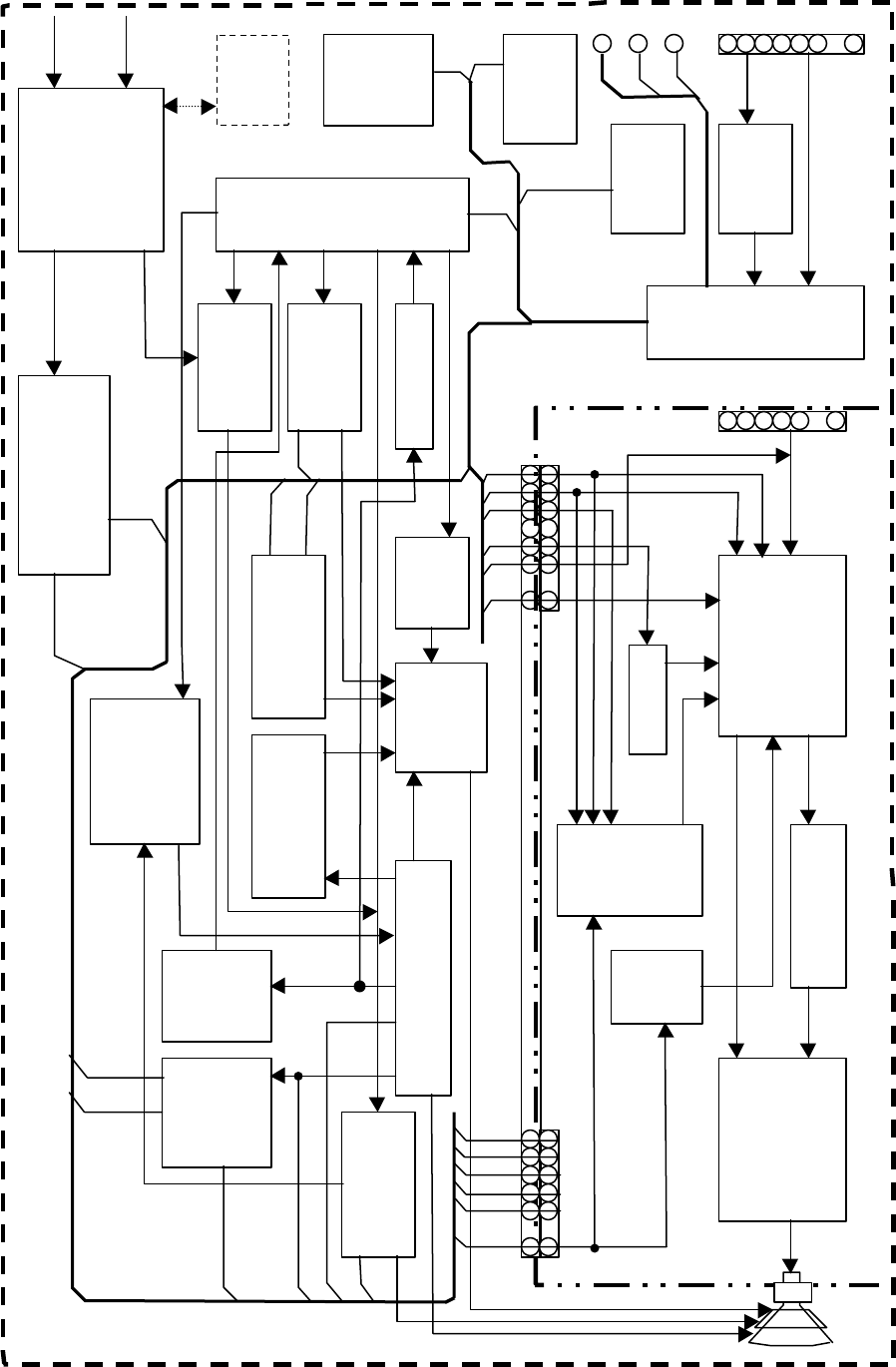
37
POWER SUPPLY
U101,U102,T101,
BD101,Q101
MCU
U701
H,V BUFFER
Q701,702
H
V
HSCL,HSDA,PC/5V,PC/#5
AC
I/P
PFC
U103
H,V
OSC
U301
POWER SAVING Q114,
Q115,116,104,105,112
76V,15V,6.3V
H-DRIVER
Q316
E/W Q309,311
CORRECTION
H-S
B+ STEP-UP
Q312,307,308
40V
DEGAUSS
Q108,110
H-O/P
Q315
HOT T302
H-LINEAR Q322
CS-SELECT Q324~7
RASTER CENTER
Q313,314
VERTICAL O/P
U401
ROTATION
Q601,602
EEPROM
U702
X-RAY
POTECT
Q339,340
DYNAMIC Q304,
FOCUS Q305,303,
Q302,338
BRIT
Q323,329,
Q331
HV ADJ
DC RESTORE
Q211,212,231,
232,251,252,
VIDEO PACK U203
VIDEO PRE-AMP
U201
OSD
U202
ABL Q272 H-BLK
Q273
6.3V
12V
GND
HBLK
G1
76V
R,G,B
ISDA
VF
ABL
ISCL
ST
CLP
CLP
ST
OSD/R,G,B,FB
VF
R,G,B,/CUT OFF
HBLK
76V,12V,
6.3V
PS1,
PS2
CS1~4
SW1~3,
HF/S
MUTE
BRIT
ISCL
ISDA
ISCL
ISDA
DEG
TILT
BRIT ,DEG,TILT,
PS1, PS2,MUTE,ST, H-
S,CS1~4,HF/S,CLP,
SW1~3,ISCL,ISDA
G1
VF
ABL
HBLK
H-S
R,G,B R,G,B