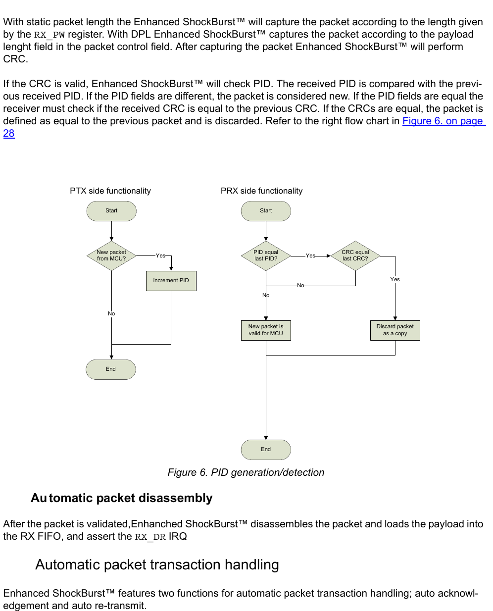
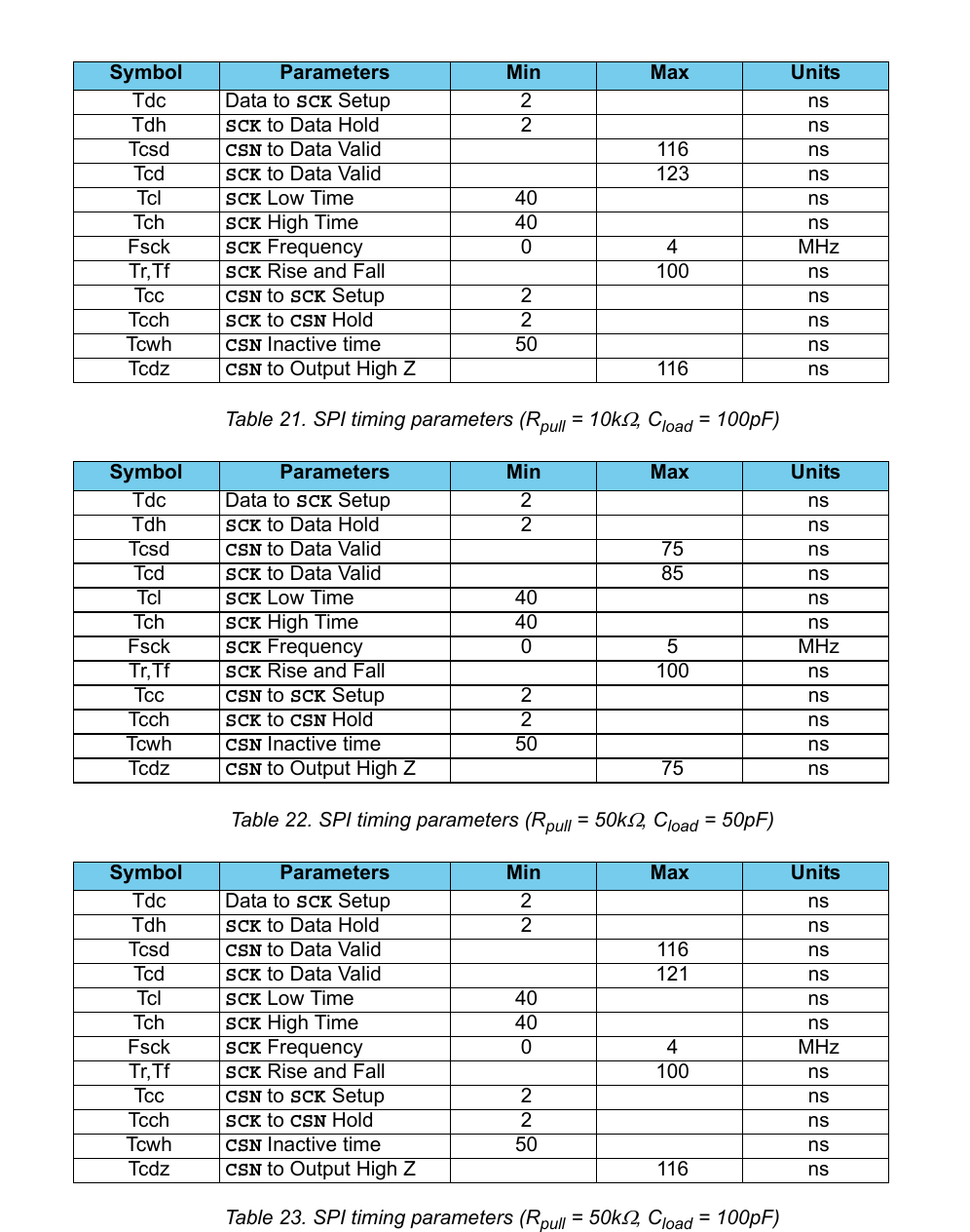
NUMA Electronics 319-NRM001 2.4G NRM User Manual nRF24L01 Product Specification V2 0
NUMA Electronics Inc. 2.4G NRM nRF24L01 Product Specification V2 0
UserManual.wiki
>
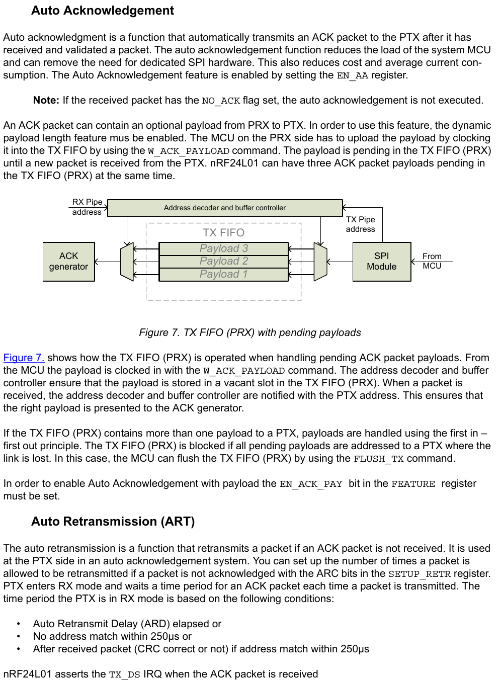
NUMA Electronics
>
319 NRM001 User Manual
User manual
Navigation menu
Upload a User Manual
Namespaces
Wiki Guide
HTML
PDF
Info
Views
User Manual
Discussion / Help
Navigation
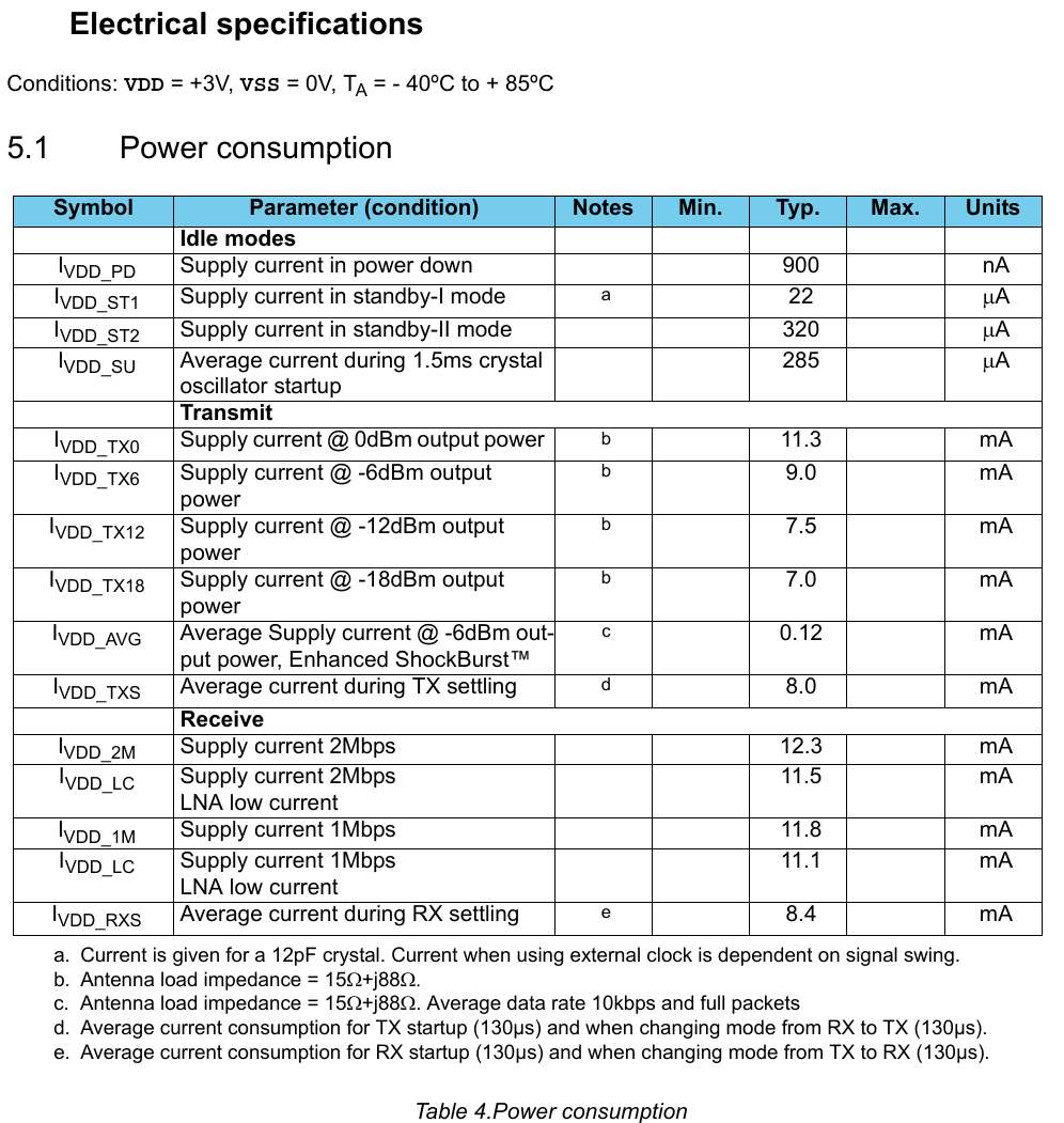
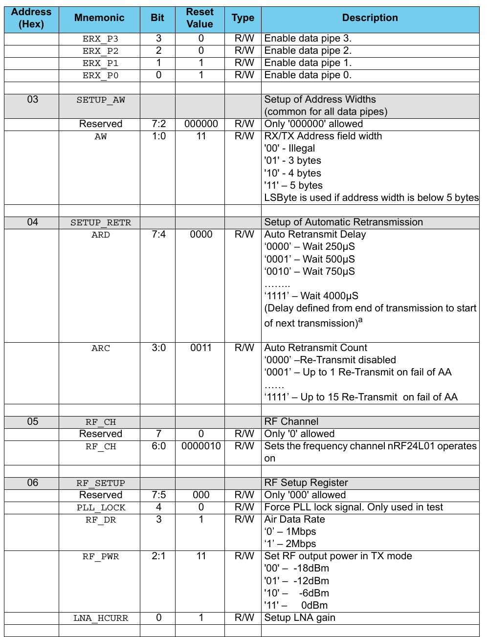
![RF channel frequencyThe RF channel frequency determines the center of the channel used by the nRF24L01. The channel occupies a bandwidth of 1MHz at 1Mbps and 2MHz at 2Mbps. nRF24L01 can operate on frequencies from 2.400GHz to 2.525GHz. The resolution of the RF channel frequency setting is 1MHz. At 2Mbps the channel occupies a bandwidth wider than the resolution of the RF channel frequency setting. To ensure non-overlapping channels in 2Mbps mode, the channel spacing must be 2MHz or more. At 1Mbps the channel bandwidth is the same as the resolution of the RF frequency setting.The RF channel frequency is set by the RF_CH register according to the following formula:F0= 2400 + RF_CH [MHz]A transmitter and a receiver must be programmed with the same RF channel frequency to be able to com-municate with each other. PA controlThe PA control is used to set the output power from the nRF24L01 power amplifier (PA). In TX mode PA control has four programmable steps, see Table 14.The PA control is set by the RF_PWR bits in the RF_SETUP register.Conditions: VDD = 3.0V, VSS = 0V, TA = 27ºC, Load impedance = 15Ω+j88Ω. Table 14. RF output power setting for the nRF24L016.5 LNA gainThe gain in the Low Noise Amplifier (LNA) in the nRF24L01 receiver is controlled by the LNA gain setting. The LNA gain makes it possible to reduce the current consumption in RX mode with 0.8mA at the cost of 1.5dB reduction in receiver sensitivity.The LNA gain has two steps and is set by the LNA_HCURR bit in the RF_SETUP register.6.6 RX/TX controlThe RX/TX control is set by PRIM_RX bit in the CONFIG register and sets the nRF24L01 in transmit/receive.SPI RF-SETUP(RF_PWR) RF output power DC current consumption11 0dBm 11.3mA10 -6dBm 9.0mA01 -12dBm 7.5mA00 -18dBm 7.0mA](https://usermanual.wiki/NUMA-Electronics/319-NRM001/User-Guide-1873057-Page-15.png)
![07 STATUS Status Register (In parallel to the SPI command word applied on the MOSI pin, the STATUS reg-ister is shifted serially out on the MISO pin)Reserved 7 0 R/W Only '0' allowedRX_DR 6 0 R/W Data Ready RX FIFO interrupt. Asserted when new data arrives RX FIFOb.Write 1 to clear bit.TX_DS 5 0 R/W Data Sent TX FIFO interrupt. Asserted when packet transmitted on TX. If AUTO_ACK is acti-vated, this bit is set high only when ACK is received.Write 1 to clear bit.MAX_RT 4 0 R/W Maximum number of TX retransmits interruptWrite 1 to clear bit. If MAX_RT is asserted it must be cleared to enable further communication. RX_P_NO 3:1 111 R Data pipe number for the payload available for reading from RX_FIFO000-101: Data Pipe Number110: Not Used111: RX FIFO EmptyTX_FULL 0 0 R TX FIFO full flag. 1: TX FIFO full. 0: Available locations in TX FIFO.08 OBSERVE_TX Transmit observe registerPLOS_CNT 7:4 0 R Count lost packets. The counter is overflow pro-tected to 15, and discontinues at max until reset. The counter is reset by writing to RF_CH. See page 65 and page 74.ARC_CNT 3:0 0 R Count retransmitted packets. The counter is reset when transmission of a new packet starts. See page 65.09 CDReserved 7:1 000000 RCD 0 0 R Carrier Detect. See page page 74.0A RX_ADDR_P0 39:0 0xE7E7E7E7E7R/W Receive address data pipe 0. 5 Bytes maximum length. (LSByte is written first. Write the number of bytes defined by SETUP_AW)0B RX_ADDR_P1 39:0 0xC2C2C2C2C2R/W Receive address data pipe 1. 5 Bytes maximum length. (LSByte is written first. Write the number of bytes defined by SETUP_AW)0C RX_ADDR_P2 7:0 0xC3 R/W Receive address data pipe 2. Only LSB. MSBy-tes is equal to RX_ADDR_P1[39:8]0D RX_ADDR_P3 7:0 0xC4 R/W Receive address data pipe 3. Only LSB. MSBy-tes is equal to RX_ADDR_P1[39:8]0E RX_ADDR_P4 7:0 0xC5 R/W Receive address data pipe 4. Only LSB. MSBy-tes is equal to RX_ADDR_P1[39:8]0F RX_ADDR_P5 7:0 0xC6 R/W Receive address data pipe 5. Only LSB. MSBy-tes is equal to RX_ADDR_P1[39:8]Address (Hex) Mnemonic Bit Reset Value Type Description](https://usermanual.wiki/NUMA-Electronics/319-NRM001/User-Guide-1873057-Page-33.png)