NUMA Electronics 319-NRM001 2.4G NRM User Manual nRF24L01 Product Specification V2 0
NUMA Electronics Inc. 2.4G NRM nRF24L01 Product Specification V2 0
User manual
Product Specification
Key Features
• Worldwide 2.4GHz ISM band operation
• Up to 2Mbps on air data rate
• Ultra low power operation
• 11.3mA TX at 0dBm output power
• 12.3mA RX at 2Mbps air data rate
• 900nA in power down
• 22µA in standby-I
• On chip voltage regulator
• 1.9 to 3.6V supply range
• Enhanced ShockBurst™
• Automatic packet handling
• Auto packet transaction handling
• 6 data pipe MultiCeiver™
319-NRM001 User's Manual
FEDERAL COMMUNICATIONS COMMISSION INTERFERENCE STATEMENT
This equipment has been tested and found to comply with the limits for a Class B digital device,
pursuant to part 15 of the FCC Rules. These limits are designed to provide reasonable protection
against harmful interference in a residential installation. This equipment generates, uses and can
radiate radio frequency energy and, if not installed and used in accordance with the instructions,
may cause harmful interference to radio communications. However, there is no guarantee that
interference will not occur in a particular installation. If this equipment does cause harmful interference
to radio or television reception, which can be determined by turning the equipment off and on, the user
is encouraged to try to correct the interference by one or more of the following measures:
-Reorient or relocate the receiving antenna.
-Increase the separation between the equipment and receiver.
-Connect the equipment into an outlet on a circuit different from that to which the receiver is connected.
-Consult the dealer or an experienced radio/ TV technician for help.
CAUTION:
Any changes or modifications not expressly approved by the grantee of this device could
void the user's authority to operate the equipment.
Labeling requirements
This device complies with Part 15 of the FCC Rules. Operation is subject to the following
two conditions: (1) this device may not cause harmful interference, and (2) this device must
accept any interference received, including interference that may cause undesired operation.
RF exposure warning
The equipment complies with FCC RF exposure limits set forth for an uncontrolled environment.
The equipment must not be co-located or operating in conjunction with any other antenna or transmitter.
End Product Labeling
This transmitter module is authorized only for use in device where the antenna may be installed such that
20cm may be maintained between the antenna and users. The final end product must be labeled in a visible
area with the following: "Contains FCC ID: YKH319-NRM001 "
Information for the OEMs and Integrators
The following statement must be included with all versions of this document supplied to an
OEM or integrator, but should not be distributed to the end user.
1) This device is intended for OEM integrators only.
2) Please see the full Grant of Equipment document for other restrictions

Features
•Radio
XWorldwide 2.4GHz ISM band operation
X126 RF channels
XCommon RX and TX pins
XGFSK modulation
X1 and 2Mbps air data rate
X1MHz non-overlapping channel spacing at 1Mbps
X2MHz non-overlapping channel spacing at 2Mbps
• Transmitter
XProgrammable output power: 0, -6, -12 or -18dBm
X11.3mA at 0dBm output power
• Receiver
XIntegrated channel filters
X12.3mA at 2Mbps
X-82dBm sensitivity at 2Mbps
X-85dBm sensitivity at 1Mbps
XProgrammable LNA gain
• RF Synthesizer
XFully integrated synthesizer
XNo external loop filer, VCO varactor diode or resonator
XAccepts low cost ±60ppm 16MHz crystal
• Enhanced ShockBurst™
X1 to 32 bytes dynamic payload length
XAutomatic packet handling
XAuto packet transaction handling
X6 data pipe MultiCeiver™ for 1:6 star networks
• Power Management
XIntegrated voltage regulator
X1.9 to 3.6V supply range
XIdle modes with fast start-up times for advanced power management
X22uA Standby-I mode, 900nA power down mode
XMax 1.5ms start-up from power down mode
XMax 130us start-up from standby-I mode
• Host Interface
X4-pin hardware SPI
XMax 8Mbps
X3 separate 32 bytes TX and RX FIFOs
X5V tolerant inputs
• Compact 20-pin 4x4mm QFN package
Absolute maximum ratings
Table 2. Absolute maximum ratings
Operating conditions Minimum Maximum Units
Supply voltages
VDD -0.3 3.6 V
VSS 0V
Input voltage
VI-0.3 5.25 V
Output voltage
VOVSS to VDD VSS to VDD
Total Power Dissipation
PD (TA=85°C) 60 mW
Temperatures
Operating Temperature -40 +85 °C
Storage Temperature -40 +125 °C

Operating conditions
Table 3. Operating conditions
Symbol Parameter (condition) Notes Min. Typ. Max. Units
VDD Supply voltage 1.9 3.0 3.6 V
VDD Supply voltage if input signals >3.6V 2.7 3.0 3.3 V
TEMP Operating Temperature -40 +27 +85 ºC

Electrical specifications
Conditions: VDD = +3V, VSS = 0V, TA = - 40ºC to + 85ºC
5.1 Power consumption
Table 4.Power consumption
Symbol Parameter (condition) Notes Min. Typ. Max. Units
Idle modes
IVDD_PD Supply current in power down 900 nA
IVDD_ST1 Supply current in standby-I mode a
a. Current is given for a 12pF crystal. Current when using external clock is dependent on signal swing.
22 μA
IVDD_ST2 Supply current in standby-II mode 320 μA
IVDD_SU Average current during 1.5ms crystal
oscillator startup
285 μA
Transmit
IVDD_TX0 Supply current @ 0dBm output power b
b. Antenna load impedance = 15Ω+j88Ω.
11.3 mA
IVDD_TX6 Supply current @ -6dBm output
power
b9.0 mA
IVDD_TX12 Supply current @ -12dBm output
power
b7.5 mA
IVDD_TX18 Supply current @ -18dBm output
power
b7.0 mA
IVDD_AVG Average Supply current @ -6dBm out-
put power, Enhanced ShockBurst™
c
c. Antenna load impedance = 15Ω+j88Ω. Average data rate 10kbps and full packets
0.12 mA
IVDD_TXS Average current during TX settling d
d. Average current consumption for TX startup (130µs) and when changing mode from RX to TX (130µs).
8.0 mA
Receive
IVDD_2M Supply current 2Mbps 12.3 mA
IVDD_LC Supply current 2Mbps
LNA low current
11.5 mA
IVDD_1M Supply current 1Mbps 11.8 mA
IVDD_LC Supply current 1Mbps
LNA low current
11.1 mA
IVDD_RXS Average current during RX settling e
e. Average current consumption for RX startup (130µs) and when changing mode from TX to RX (130µs).
8.4 mA

General RF conditions
Table 5. General RF conditions
Transmitter operation
Table 6.Transmitter operation
Symbol Parameter (condition) Notes Min. Typ. Max. Units
fOP Operating frequency a
a. Usable band is determined by local regulations
2400 2525 MHz
PLLres PLL Programming resolution 1 MHz
fXTAL Crystal frequency 16 MHz
Δf1M Frequency deviation @ 1Mbps ±160 kHz
Δf2M Frequency deviation @ 2Mbps ±320 kHz
RGFSK Air Data rate b
b. Data rate in each burst on-air
1000 2000 kbps
FCHAN-
NEL 1M
Non-overlapping channel spac-
ing @ 1Mbps
c
c. The minimum channel spacing is 1Mhz
1MHz
FCHAN-
NEL 2M
Non-overlapping channel spac-
ing @ 2Mbps
c2MHz
Symbol Parameter (condition) Notes Min. Typ. Max. Units
PRF Maximum Output Power a
a. Antenna load impedance = 15Ω+j88Ω
0+4dBm
PRFC RF Power Control Range 16 18 20 dB
PRFCR RF Power Accuracy ±4 dB
PBW2 20dB Bandwidth for Modulated Carrier
(2Mbps)
1800 2000 kHz
PBW1 20dB Bandwidth for Modulated Carrier
(1Mbps)
900 1000 kHz
PRF1 1st Adjacent Channel Transmit Power
2MHz
-20 dBm
PRF2 2nd Adjacent Channel Transmit Power
4MHz
-50 dBm

Receiver operation
Table 7. Receiver operation
Symbol Parameter (condition) Notes Min. Typ. Max. Units
RXmax Maximum received signal at <0.1% BER 0 dBm
RXSENS Sensitivity (0.1%BER) @2Mbps -82 dBm
RXSENS Sensitivity at (0.1%BER) @1Mbps -85 dBm
RX selectivity according to ETSI EN 300 440-1 V1.3.1 (2001-09) page 27
C/ICO C/I Co-channel (@2Mbps) a
a. Data rate is 2Mbps for the following C/I measurements
7dB
C/I1ST 1st Adjacent Channel Selectivity C/I 2MHz 1dB
C/I2ND 2nd Adjacent Channel Selectivity C/I 4MHz -21 dB
C/I3RD 3rd Adjacent Channel Selectivity C/I 6MHz -27 dB
C/ICO C/I Co-channel (@1Mbps) b
b. Data rate is 1Mbps for the following C/I measurements
9dB
C/I1ST 1st Adjacent Channel Selectivity C/I 1MHz 8dB
C/I2ND 2nd Adjacent Channel Selectivity C/I 2MHz -22 dB
C/I3RD 3rd Adjacent Channel Selectivity C/I 3MHz -30 dB
RX selectivity with nRF24L01 equal modulation on interfering signal
C/ICO C/I Co-channel (@2Mbps) (Modulated car-
rier)
a11 dB
C/I1ST 1st Adjacent Channel Selectivity C/I 2MHz 4dB
C/I2ND 2nd Adjacent Channel Selectivity C/I 4MHz -20 dB
C/I3RD 3rd Adjacent Channel Selectivity C/I 6MHz -27 dB
C/ICO C/I Co-channel (@1Mbps) b12 dB
C/I1ST 1st Adjacent Channel Selectivity C/I 1MHz 8dB
C/I2ND 2nd Adjacent Channel Selectivity C/I 2MHz -21 dB
C/I3RD 3rd Adjacent Channel Selectivity C/I 3MHz -30 dB
Crystal specifications
Table 8. Crystal specifications
Symbol Parameter (condition) Notes Min. Typ. Max. Units
Fxo Crystal Frequency 16 MHz
ΔF Tolerance a b
a. Frequency accuracy including; tolerance at 25ºC, temperature drift, aging and crystal loading.
b. Frequency regulations in certain regions sets tighter requirements to frequency tolerance (Ex:
Japan and Korea max. +/- 50ppm)
±60 ppm
C0Equivalent parallel capacitance 1.5 7.0 pF
CLLoad capacitance 8 12 16 pF
ESR Equivalent Series Resistance 100 Ω
DC characteristics
Table 9. Digital input pin
Table 10. Digital output pin
Power on reset
Table 11. Power on reset
Symbol Parameter (condition) Notes Min. Typ. Max. Units
VIH HIGH level input voltage 0.7VDD 5.25aV
VIL LOW level input voltage VSS 0.3VDD V
Symbol Parameter (condition) Notes Min. Typ. Max. Units
VOH HIGH level output voltage (IOH=-0.25mA) VDD -0.3 VDD V
VOL LOW level output voltage (IOL=0.25mA) 0.3 V
Symbol Parameter (condition) Notes Min. Typ. Max. Units
TPUP Power ramp up time a
a. From 0V to 1.9V
100 ms
TPOR Power on reset b
b. Measured when the VDD reaches 1.9V to when the reset finishes
1.6 5.3 10.3 ms

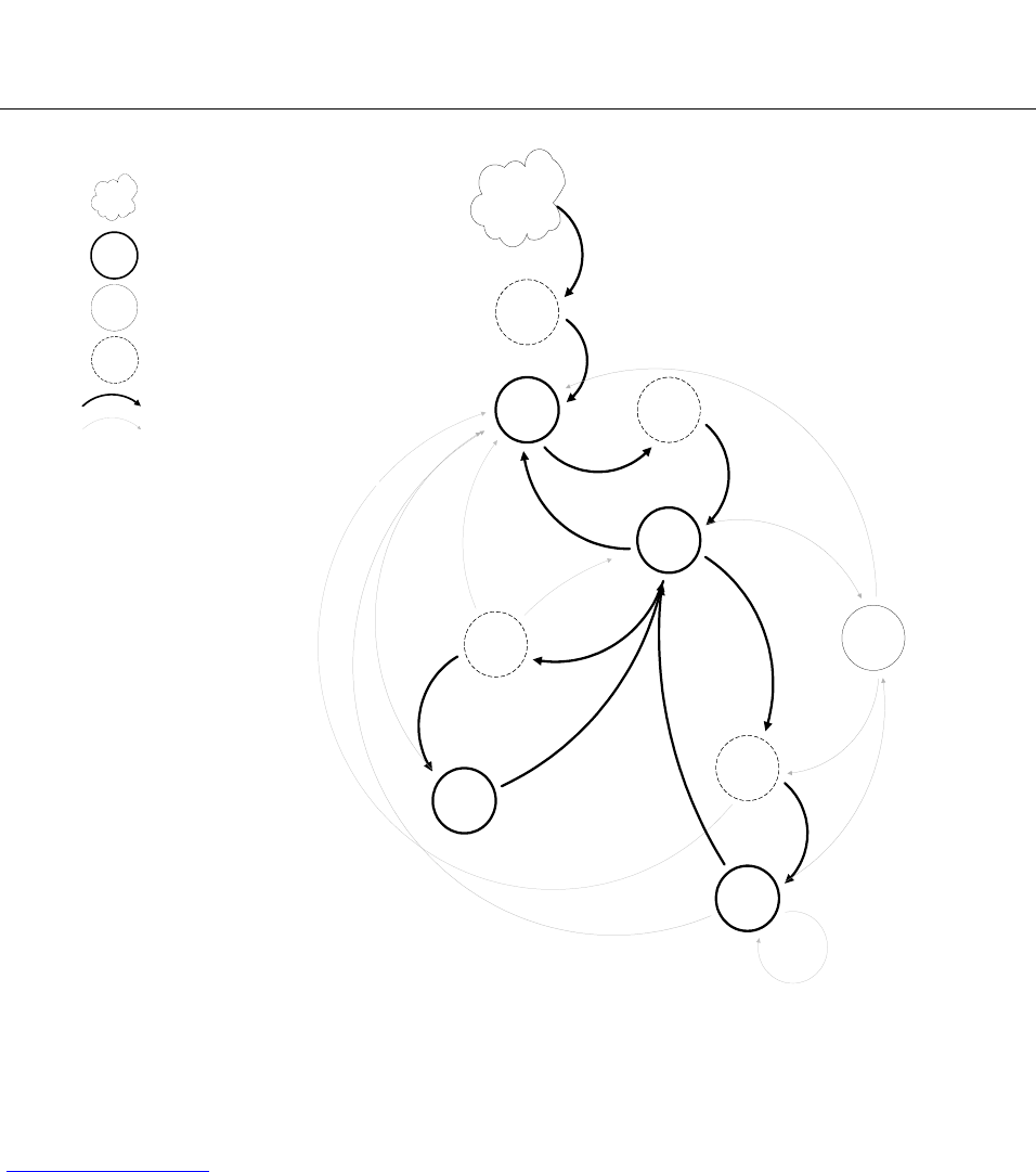
Radio Control
This chapter describes the different modes the 319-NRM001 radio transceiver can operate in and the param-
eters used to control the radio.
The 319-NRM001 has a built-in state machine that controls the transitions between the different operating
modes of the chip. The state machine takes input from user defined register values and internal signals.
Operational Modes
The 319-NRM001 can be configured in four main modes of operation. This section describes these modes.
.
Figure 3. Radio control state diagram
Power Down Mode
In power down mode 319-nrm0011 is disabled with minimal current consumption. In power down mode all the
register values available from the SPI are maintained and the SPI can be activated. For start up time see
Table 13. on page 22. Power down mode is entered by setting the PWR_UP bit in the CONFIG register low.
Standby Modes
By settting the PWR_UP bit in the CONFIG register to 1, the device enters standby-I mode. Standby-I mode
is used to minimize average current consumption while maintaining short start up times. In this mode part
of the crystal oscillator is active. This is the mode the nRF24L01 returns to from TX or RX mode when CE
is set low.
In standby-II mode extra clock buffers are active compared to standby-I mode and much more current is
used compared to standby-I mode. Standby-II occurs when CE is held high on a PTX device with empty TX
FIFO. If a new packet is uploaded to the TX FIFO, the PLL starts and the packet is transmitted.
VDD >= 1.9V
Undefined
Power on
reset
10.3ms
Power Down
Standby-I
RX Mode
TX Mode
Standby-II
RX Settling
130 us
Start up
1.5ms
PWR_UP = 1
PWR_UP = 0
TX Settling
130 us
TX FIFO not empty
PRIM_RX = 0
CE = 1 for more than 10µs
PRIM_RX = 1
CE = 1
CE = 0
TX FIFO empty
CE = 1
TX FIFO not empty
CE = 1
PRIM_RX = 0
TX FIFO empty
CE = 1
PWR_UP = 0
PWR_UP = 0
PWR_UP=0
CE = 0
PWR_UP=0
PWR_UP=0
TX finished with one packet
CE = 0
CE = 1
TX FIFO not empty
Possible operating mode
Recommended path between operating modes
Possible path between operating modes
Recommended operating mode
Transition state
CE = 1 Pin signal condition
PWR_DN = 1 Bit state condition
Undefined
TX FIFO empty System information
Undefined
Legend:

The register values are maintained during standby modes and the SPI may be activated. For start up time
see Table 13. on page 22.
RX mode
The RX mode is an active mode where the 319-NRM001 radio is a receiver. To enter this mode, the
319-NRM001 must have the PWR_UP bit set high, PRIM_RX bit set high and the CE pin set high.
In this mode the receiver demodulates the signals from the RF channel, constantly presenting the demod-
ulated data to the baseband protocol engine. The baseband protocol engine constantly searches for a
valid packet. If a valid packet is found (by a matching address and a valid CRC) the payload of the packet
is presented in a vacant slot in the RX FIFO. If the RX FIFO is full, the received packet is discarded.
The 319-NRM001 remains in RX mode until the MCU configures it to standby-I mode or power down mode. If
the automatic protocol features (Enhanced ShockBurst™) in the baseband protocol engine are enabled,
the 319-NRM001 can enter other modes in order to execute the protocol.
In RX mode a carrier detect signal is avaliable. The carrier detect is a signal that is set high when a RF sig-
nal is detected inside the receiving frequency channel. The signal must be FSK modulated for a secure
detection. Other signals can also be detected. The Carrier Detect (CD) is set high when an RF signal is
detected in RX mode, otherwise CD is low. The internal CD signal is filtered before presented to CD register.
The RF signal must be present for at least 128µs before the CD is set high. How to use the CD is described
in Appendix E on page 74.
TX mode
The TX mode is an active mode where the nRF24L01 transmits a packet. To enter this mode, the
319-NRM001 must have the PWR_UP bit set high, PRIM_RX bit set low, a payload in the TX FIFO and, a high
pulse on the CE for more than 10µs.
The 319-NRM001 stays in TX mode until it finishes transmitting a current packet. If CE = 0 nRF24L01 returns
to standby-I mode. If CE = 1, the next action is determined by the status of the TX FIFO. If the TX FIFO is
not empty the 319-NRM0001 remains in TX mode, transmitting the next packet. If the TX FIFO is empty the
319-NRM001 goes into standby-II mode.The 319-NRM001 transmitter PLL operates in open loop when in TX
mode. It is important to never keep the 319-NRM001 in TX mode for more than 4ms at a time. If the auto
retransmit is enabled, the 319-NRM001 is never in TX mode long enough to disobey this rule.
Operat ional modes configuration
The following table (Table 12.) describes how to configure the operational modes.
Mode PWR_UP
register
PRIM_RX
register CE FIFO state
RX mode111-
TX mode 1 0 1 Data in TX FIFO. Will empty all lev-
els in TX FIFOa.
TX mode 1 0 minimum 10μs
high pulse
Data in TX FIFO.Will empty one
level in TX FIFOb.
Standby-II 1 0 1 TX FIFO empty
Standby-I 1 - 0 No ongoing packet transmission
Power Down 0 - - -
Timing Information
The timing information in this section is related to the transitions between modes and the timing for the CE
pin. The transition from TX mode to RX mode or vice versa is the same as the transition from standby-I to
TX mode or RX mode,Tstby2a.
Table 13. Operational timing of nRF24L01
When 319-NRM001is in power down mode it must settle for 1.5ms before it can enter the TX or RX modes. If
an external clock is used this delay is reduced to 150µs, see Table 13. on page 22. The settling time must
be controlled by the MCU.
Air data rate
The air data rate is the modulated signaling rate the nRF24L01 uses when transmitting and receiving data.
The air data rate can be 1Mbps or 2Mbps. The 1Mbps data rate gives 3dB better receiver sensitivity com-
pared to 2Mbps. High air data rate means lower average current consumption and reduced probability of
on-air collisions.
The air data rate is set by the RF_DR bit in the RF_SETUP register.
A transmitter and a receiver must be programmed with the same air data rate to be able to communicate
with each other.
For compatibility with nRF2401A, nRF24E1, nRF2402 and nRF24E2 the air data rate must be set to
1Mbps.
a. In this operating mode if the CE is held high the TX FIFO is emptied and all necessary ACK and pos-
sible retransmits are carried out. The transmission continues as long as the TX FIFO is refilled. If the
TX FIFO is empty when the CE is still high, nRF24L01 enters standby-II mode. In this mode the trans-
mission of a packet is started as soon as the CSN is set high after a upload (UL) of a packet to TX
FIFO.
b. This operating mode pulses the CE high for at least 10µs. This allows one packet to be transmitted.
This is the normal operating mode. After the packet is transmittet, the nRF24L01 enters standby-I
mode.
Name nRF24L01 Max. Min. Comments
Tpd2stby Power Down Î Standby mode 1.5ms Internal crystal
oscillator
Tpd2stby Power Down Î Standby mode 150µs With external
clock
Tstby2a Standby modes Î TX/RX mode 130µs
Thce Minimum CE high 10µs
Tpece2csn Delay from CE pos. edge to CSN low 4µs
RF channel frequency
The RF channel frequency determines the center of the channel used by the nRF24L01. The channel
occupies a bandwidth of 1MHz at 1Mbps and 2MHz at 2Mbps. nRF24L01 can operate on frequencies from
2.400GHz to 2.525GHz. The resolution of the RF channel frequency setting is 1MHz.
At 2Mbps the channel occupies a bandwidth wider than the resolution of the RF channel frequency setting.
To ensure non-overlapping channels in 2Mbps mode, the channel spacing must be 2MHz or more. At
1Mbps the channel bandwidth is the same as the resolution of the RF frequency setting.
The RF channel frequency is set by the RF_CH register according to the following formula:
F0= 2400 + RF_CH [MHz]
A transmitter and a receiver must be programmed with the same RF channel frequency to be able to com-
municate with each other.
PA control
The PA control is used to set the output power from the nRF24L01 power amplifier (PA). In TX mode PA
control has four programmable steps, see Table 14.
The PA control is set by the RF_PWR bits in the RF_SETUP register.
Conditions: VDD = 3.0V, VSS = 0V, TA = 27ºC, Load impedance = 15Ω+j88Ω.
Table 14. RF output power setting for the nRF24L01
6.5 LNA gain
The gain in the Low Noise Amplifier (LNA) in the nRF24L01 receiver is controlled by the LNA gain setting.
The LNA gain makes it possible to reduce the current consumption in RX mode with 0.8mA at the cost of
1.5dB reduction in receiver sensitivity.
The LNA gain has two steps and is set by the LNA_HCURR bit in the RF_SETUP register.
6.6 RX/TX control
The RX/TX control is set by PRIM_RX bit in the CONFIG register and sets the nRF24L01 in transmit/
receive.
SPI RF-SETUP
(RF_PWR) RF output power DC current
consumption
11 0dBm 11.3mA
10 -6dBm 9.0mA
01 -12dBm 7.5mA
00 -18dBm 7.0mA

Enhanced ShockBurst™
Enhanced ShockBurst™ is a packet based data link layer. It features automatic packet assembly and tim-
ing, automatic acknowledgement and re-transmissions of packets. Enhanced ShockBurst™ enables the
implementation of ultra low power, high performance communication with low cost host microcontrollers.
The features enable significant improvements of power efficiency for bi-directional and uni-directional sys-
tems, without adding complexity on the host controller side.
Features
The main features of Enhanced ShockBurst™ are:
• 1 to 32 bytes dynamic payload length
• Automatic packet handling
• Auto packet transaction handling
XAuto Acknowledgement
XAuto retransmit
• 6 data pipe MultiCeiver™ for 1:6 star networks
Enhanced ShockBurst™ overview
Enhanced ShockBurst™ uses ShockBurst™ for automatic packet handling and timing. During transmit,
ShockBurst™ assembles the packet and clocks the bits in the data packet into the transmitter for transmis-
sion. During receive, ShockBurst™ constantly searches for a valid address in the demodulated signal.
When ShockBurst™ finds a valid address, it processes the rest of the packet and validates it by CRC. If
the packet is valid the payload is moved into the RX FIFO. The high speed bit handling and timing is con-
trolled by ShockBurst™.
Enhanced ShockBurst™ features automatic packet transaction handling that enables the implementation
of a reliable bi-directional data link. An Enhanced ShockBurst™ packet transaction is a packet exchange
between to transceivers, where one transceiver is the Primary Receiver (PRX) and the other is the Primary
Transmitter (PTX). An Enhanced ShockBurst™ packet transaction is always initiated by a packet transmis-
sion from the PTX, the transaction is complete when the PTX has received an acknowledgment packet
(ACK packet) from the PRX.
The automatic packet transaction handling works as follows:
• The user initiates the transaction by transmitting a data packet from the PTX to the PRX. Enhanced
ShockBurst™ automatically sets the PTX in receive mode to wait for the ack packet.
• If the packet is received by the PRX, Enhanced ShockBurst™ automatically assembles and trans-
mits an acknowledgment packet (ACK packet) to the PTX before returning to receive mode
• If the PTX does not receive the ACK packet within a set time, Enhanced ShockBurst™ will automat-
ically retransmit the original data packet and set the PTX in receive mode to wait for the ACK packet
The PRX can attach user data to the ACK packet enabling a bi-directional data link. The Enhanced Shock-
Burst™ is highly configurable; it is possible to configure parameters such as maximum number of retrans-
mits and the delay from one transmission to the next retransmission. All automatic handling is done without
involvement of the MCU.
Section 7.3 on page 25 gives a description of the Enhanced ShockBurst packet format, section 7.4 on
page 26 describes autmatic packet handling, section 7.5 on page 28 describes automatic packet transac-
tion handling, section 7.6 on page 31 provides flowcharts for PTX and PRX operation.

Enhanced Shockburst™ packet format
The format of the Enhanced ShockBurst™ packet is described in this chapter. The Enhanched Shock-
Burst™ packet contains a preamble field, address field, packet control field, payload field and a CRC field.
Figure 4. on page 25 shows the packet format with MSB to the left.
Figure 4. An Enhanced ShockBurst™ packet with payload (0-32 bytes)
Preamble
The preamble is a bit sequence used to detect 0 and 1 levels in the receiver. The preamble is one byte
long and is either 01010101 or 10101010. If the first bit in the address is 1 the preamble is automatically
set to 10101010 and if the first bit is 0 the preamble is automatically set to 01010101. This is done to
ensure there are enough transitions in the preamble to stabilize the receiver.
Address
This is the address for the receiver. An address ensures that the correct packet are detected by the
receiver. The address field can be configured to be 3, 4 or, 5 bytes long with the AW register.
Note: Addresses where the level shifts only one time (that is, 000FFFFFFF) can often be detected in
noise and can give a false detection, which may give a raised Packet-Error-Rate. Addresses
as a continuation of the preamble (hi-low toggling) raises the Packet-Error-Rate.
Pa cket Control Field
Figure 5 shows the format of the 9 bit packet control field, MSB to the left.
Figure 5. Packet control field
The packet control field contains a 6 bit payload length field, a 2 bit PID (Packet Identity) field and, a 1 bit
NO_ACK flag.
7.3.3.1 Payload length
This 6 bit field specifies the length of the payload in bytes. The length of the payload can be from 0 to 32
bytes.
Preamble 1 byte Address 3-5 byte 9 bit Payload 0 - 32 byte CRC 1-2
byte
Packet Control Field
NO_ACK 1bitPID 2bitPayload length 6bit

Coding: 000000 = 0 byte (only used in empty ACK packets.) 100000 = 32 byte, 100001 = Don’t care.
This field is only used if the Dynamic Payload Length function is enabled.
PID (Packet identification)
The 2 bit PID field is used to detect if the received packet is new or retransmitted. PID prevents the PRX
device from presenting the same payload more than once to the MCU. The PID field is incremented at the
TX side for each new packet received through the SPI. The PID and CRC fields (see section 7.3.5 on page
26) are used by the PRX device to determine if a packet is retransmitted or new. When several data pack-
ets are lost on the link, the PID fields may become equal to the last received PID. If a packet has the same
PID as the previous packet, nRF24L01 compares the CRC sums from both packets. If the CRC sums are
also equal, the last received packet is considered a copy of the previously received packet and discarded.
No Acknowledgment flag(NO_ACK)
The Selective Auto Acknowledgement feature controls the NO_ACK flag.
This flag is only used when the auto acknowledgement feature is used. Setting the flag high, tells the
receiver that the packet is not to be auto acknowledged.
Payload
The payload is the user defined content of the packet. It can be 0 to 32 bytes wide and is transmitted on-air
as it is uploaded (unmodified) to the device.
CRC (Cyclic Redundancy Check)
The CRC is the error detection mechanism in the packet. It may either be 1 or 2 bytes and is calculated
over the address, Packet Control Field, and Payload.
The polynomial for 1 byte CRC is X8 + X2 + X + 1. Initial value 0xFF
The polynomial for 2 byte CRC is X16+ X12 + X5 + 1. Initial value 0xFFFF
No packet is accepted by Enhanced ShockBurst™ if the CRC fails.
Automatic packet handling
Enhanced ShockBurst™ uses ShockBurst™ for automatic packet handling. The functions are static and
dynamic payload length, automatic packet assembly, automatic packet validation and automatic packet
disassembly.
Static and Dynamic Payload Length
The Enhanced ShockBurst™ provides two alternatives for handling payload lengths, static and dynamic.
The default alternative is static payload length. With static payload length all packets between a transmitter
and a receiver have the same length. Static payload length is set by the RX_PW_Px registers on the
receiver side. The payload length on the transmitter side is set by the number of bytes clocked into the
TX_FIFO and must equal the value in the RX_PW_Px register on the receiver side
Dynamic Payload Length(DPL) is an alternative to static payload length.DPL enables the transmitter to
send packets with variabel payload length to the receiver. This means for a system with different payload
lenghts it is not necessary to scale the packet length to the longest payload.

With DPL feature the nRF24L01 can decode the payload length of the received packet automatically
instead of using the RX_PW_Px registers. The MCU can read the length of the received payload by using
the R_RX_PL_WID command.
In order to enable DPL the EN_DPL bit in the FEATURE register must be set. In RX mode the DYNPD reg-
ister has to be set. A PTX that transmits to a PRX with DPL enabled must have the DPL_P0 bit in DYNPD
set.
Au tomatic packet assembly
The automatic packet assembly assembles the preamble, address, packet control field, payload and CRC
to make a complete packet before it is transmitted.
Preamble
The preamble is automaticly generated based on the address field.
Address
The address is fetched from the TX_ADDR register. The address field can be configured to be 3, 4 or 5
bytes long with the AW register.
Packet control field
For the static packet lenght option the payload length field is not used. With DPL enabled, the value in the
payload length field is automaticly set to the number of bytes in the payload clocked into the TX FIFO.
The transmitter increments the PID field each time it generates a new packet and uses the same PID on
packets that are retransmitted. Refer to the left flow chart in Figure 6. on page 28
The PTX can set the NO_ACK flag bit in the Packet Control Field with this command:
W_TX_PAYLOAD_NOACK
However, the function must first be enabled in the FEATURE register by setting the EN_DYN_ACK bit.
When you use this option the PTX goes directly to standby-I mode after transmitting the packet and the
PRX does not transmit an ACK packet when it receives the packet.
Payload
The payload is fetched from the TX FIFO.
CRC
The CRC is automaticly calculated based on the packet content with the polynomials in 7.3.5 on page 26.
The number of bytes in the CRC is set by the CRCO bit in the CONFIG register.
Automatic packet validation
Enhanced ShockBurst™ features automatic packet validation. In receive mode the nRF24L01 is constanly
searching for a valid address (given in the RX_ADDR registers.) If a valid address is detected the
Enhanched ShockBurst™ will start to validate the packet.
With static packet length the Enhanced ShockBurst™ will capture the packet according to the length given
by the RX_PW register. With DPL Enhanced ShockBurst™ captures the packet according to the payload
lenght field in the packet control field. After capturing the packet Enhanced ShockBurst™ will perform
CRC.
If the CRC is valid, Enhanced ShockBurst™ will check PID. The received PID is compared with the previ-
ous received PID. If the PID fields are different, the packet is considered new. If the PID fields are equal the
receiver must check if the received CRC is equal to the previous CRC. If the CRCs are equal, the packet is
defined as equal to the previous packet and is discarded. Refer to the right flow chart in Figure 6. on page
28
Figure 6. PID generation/detection
Au tomatic packet disassembly
After the packet is validated,Enhanched ShockBurst™ disassembles the packet and loads the payload into
the RX FIFO, and assert the RX_DR IRQ
Automatic packet transaction handling
Enhanced ShockBurst™ features two functions for automatic packet transaction handling; auto acknowl-
edgement and auto re-transmit.
Start
New packet
from MCU? Yes
increment PID
End
Start
PID equal
last PID? Yes CRC equal
last CRC?
New packet is
valid for MCU
End
No
Discard packet
as a copy
No
Yes
PTX side functionality PRX side functionality
No
Auto Acknowledgement
Auto acknowledgment is a function that automatically transmits an ACK packet to the PTX after it has
received and validated a packet. The auto acknowledgement function reduces the load of the system MCU
and can remove the need for dedicated SPI hardware. This also reduces cost and average current con-
sumption. The Auto Acknowledgement feature is enabled by setting the EN_AA register.
Note: If the received packet has the NO_ACK flag set, the auto acknowledgement is not executed.
An ACK packet can contain an optional payload from PRX to PTX. In order to use this feature, the dynamic
payload length feature mus be enabled. The MCU on the PRX side has to upload the payload by clocking
it into the TX FIFO by using the W_ACK_PAYLOAD command. The payload is pending in the TX FIFO (PRX)
until a new packet is received from the PTX. nRF24L01 can have three ACK packet payloads pending in
the TX FIFO (PRX) at the same time.
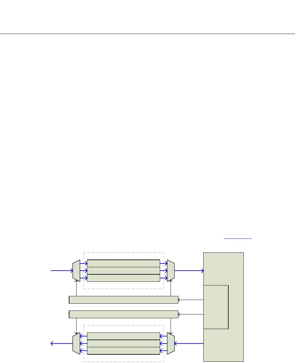
Figure 7. TX FIFO (PRX) with pending payloads
Figure 7. shows how the TX FIFO (PRX) is operated when handling pending ACK packet payloads. From
the MCU the payload is clocked in with the W_ACK_PAYLOAD command. The address decoder and buffer
controller ensure that the payload is stored in a vacant slot in the TX FIFO (PRX). When a packet is
received, the address decoder and buffer controller are notified with the PTX address. This ensures that
the right payload is presented to the ACK generator.
If the TX FIFO (PRX) contains more than one payload to a PTX, payloads are handled using the first in –
first out principle. The TX FIFO (PRX) is blocked if all pending payloads are addressed to a PTX where the
link is lost. In this case, the MCU can flush the TX FIFO (PRX) by using the FLUSH_TX command.
In order to enable Auto Acknowledgement with payload the EN_ACK_PAY bit in the FEATURE register
must be set.
Auto Retransmission (ART)
The auto retransmission is a function that retransmits a packet if an ACK packet is not received. It is used
at the PTX side in an auto acknowledgement system. You can set up the number of times a packet is
allowed to be retransmitted if a packet is not acknowledged with the ARC bits in the SETUP_RETR register.
PTX enters RX mode and waits a time period for an ACK packet each time a packet is transmitted. The
time period the PTX is in RX mode is based on the following conditions:
• Auto Retransmit Delay (ARD) elapsed or
• No address match within 250µs or
• After received packet (CRC correct or not) if address match within 250µs
nRF24L01 asserts the TX_DS IRQ when the ACK packet is received
TX FIFO
Payload 1
Payload 2
Payload 3
Address decoder and buffer controller
SPI
Module
ACK
generator
RX Pipe
address TX Pipe
address
From
MCU

nRF24L01 enters standby-I mode if there is no more untransmitted data in the TX FIFO and the CE pin is
low. If the ACK packet is not received, nRF24L01 goes back to TX mode after a delay defined by ARD and
retransmits the data. This continues until acknowledgment is received, or the maximum number of retrans-
mits is reached. Set PWR_UP =0 to abort auto retransmission. Two packet loss counters are incremented
each time a packet is lost, ARC_CNT and PLOS_CNT in the OBSERVE_TX register. The ARC_CNT counts
the number of retransmissions for the current transaction. The PLOS_CNT counts the total number of
retransmissions since the last channel change. You reset ARC_CNT by initiating a new transaction. You
reset PLOS_CNT by writing to the RF_CH register. It is possible to use the information in the OBSERVE_TX
register to make a overall assessment of the channel quality.
The ARD defines the time from the end of a transmitted packet to a retransmit starts on the PTX side. ARD
is set in SETUP_RETR register in steps of 250µs. A retransmit is made if no ACK packet is received by the
PTX.
There is a restriction for the length of ARD when using ACK packets with payload. The ARD time must
never be shorter than the sum of the startup time and the time on-air for the ACK packet.
For 1Mbps data rate and 5 byte address; 5 byte is maximum ACK packet payload length for ARD=250µs
(reset value).
For 2Mbps data rate and 5 byte address; 15 byte is maximum ACK packet payload length for ARD=250µs
(reset value).
ARD=500µs will be long enough for any payload length.
As an alternative to Auto Retransmit it is possible to manually set the nRF24L01 to retransmit a packet a
number of times. This is done by the REUSE_TX_PL command. The MCU must initiate each transmission
of the packet with the CE pin after this command has been used.

Data and Control Interface
The data and control interface gives you access to all the features in the nRF24L01. The data and control
interface consists of the following six 5Volt tolerant digital signals:
•IRQ (this signal is active low and is controlled by three maskable interrupt sources)
•CE (this signal is active high and is used to activate the chip in RX or TX mode)
•CSN (SPI signal)
•SCK (SPI signal)
•MOSI (SPI signal)
•MISO (SPI signal)
You can use the SPI to activate the nRF24L01 data FIFOs or the register map by 1 byte SPI commands
during all modes of operation.
Features
• Special SPI commands for quick access to the most frequently used features
• 0-8Mbps 4-wire SPI serial interface
• 8 bit command set
• Easily configurable register map
• Full three level FIFO for both TX and RX direction
Functional description
The SPI is a standard SPI with a maximum data rate of 8Mbps.
SPI operation
This chapter describes the SPI commands and SPI timing.
SPI Commands
The SPI commands are shown in Table 16.. Every new command must be started by a high to low transi-
tion on CSN.
In parallel to the SPI command word applied on the MOSI pin, the STATUS register is shifted serially out on
the MISO pin.
The serial shifting SPI commands is in the following format:
<Command word: MSBit to LSBit (one byte)>
<Data bytes: LSByte to MSByte, MSBit in each byte first>

Command name Command
word (binary) # Data bytes Operation
R_REGISTER 000A AAAA 1 to 5
LSByte first
Read command and status registers. AAAAA =
5 bit Register Map Address
W_REGISTER 001A AAAA 1 to 5
LSByte first
Write command and status registers. AAAAA = 5
bit Register Map Address
Executable in power down or standby modes
only.
R_RX_PAYLOAD 0110 0001 1 to 32
LSByte first
Read RX-payload: 1 – 32 bytes. A read operation
always starts at byte 0. Payload is deleted from
FIFO after it is read. Used in RX mode.
W_TX_PAYLOAD 1010 0000 1 to 32
LSByte first
Write TX-payload: 1 – 32 bytes. A write operation
always starts at byte 0 used in TX payload.
FLUSH_TX 1110 0001 0 Flush TX FIFO, used in TX mode
FLUSH_RX 1110 0010 0 Flush RX FIFO, used in RX mode
Should not be executed during transmission of
acknowledge, that is, acknowledge package will
not be completed.
REUSE_TX_PL 1110 0011 0 Used for a PTX device
Reuse last transmitted payload. Packets are
repeatedly retransmitted as long as CE is high.
TX payload reuse is active until
W_TX_PAYLOAD or FLUSH TX is executed. TX
payload reuse must not be activated or deacti-
vated during package transmission
ACTIVATE 0101 0000 1 This write command followed by data 0x73 acti-
vates the following features:
• R_RX_PL_WID
• W_ACK_PAYLOAD
• W_TX_PAYLOAD_NOACK
A new ACTIVATE command with the same data
deactivates them again. This is executable in
power down or stand by modes only.
The R_RX_PL_WID, W_ACK_PAYLOAD, and
W_TX_PAYLOAD_NOACK features registers are
initially in a deactivated state; a write has no
effect, a read only results in zeros on MISO. To
activate these registers, use the ACTIVATE com-
mand followed by data 0x73. Then they can be
accessed as any other register in nRF24L01. Use
the same command and data to deactivate the
registers again.
R_RX_PL_WIDa0110 0000 Read RX-payload width for the top
R_RX_PAYLOAD in the RX FIFO.
W_ACK_PAYLOADa1010 1PPP 1 to 32
LSByte first
Used in RX mode.
Write Payload to be transmitted together with
ACK packet on PIPE PPP. (PPP valid in the
range from 000 to 101). Maximum three ACK
packet payloads can be pending. Payloads with
same PPP are handled using first in - first out
principle. Write payload: 1– 32 bytes. A write
operation always starts at byte 0.
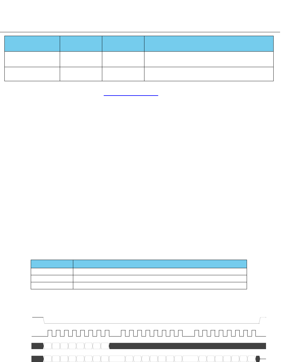
Table 16. Command set for the nRF24L01 SPI
The W_REGISTER and R_REGISTER commands can operate on single or multi-byte registers. When
accessing multi-byte registers you read or write to the MSBit of LSByte first. You can terminate the writing
before all bytes in a multi-byte register are written, leaving the unwritten MSByte(s) unchanged. For exam-
ple, the LSByte of RX_ADDR_P0 can be modified by writing only one byte to the RX_ADDR_P0 register. The
content of the status register is always read to MISO after a high to low transition on CSN.
Note: The 3 bit pipe information in the STATUS register is updated during the IRQ pin high to low
transition. If the STATUS register is read during an IRQ pin high to low transition, the pipe
information is unreliable.
SPI timing
Table 17. Abbreviations used in Figure 23. to Figure 25.
Figure 23. SPI read operation
W_TX_PAYLOAD_NO
ACKa
1011 000 1 to 32
LSByte first
Used in TX mode. Disables AUTOACK on this
specific packet.
NOP 1111 1111 0 No Operation. Might be used to read the STATUS
register
a. To activate this feature use the ACTIVATE SPI command followed by data 0x73. The corresponding bits
in the FEATURE register shown in Table 24. on page 58 have to be set.
Abbreviation Description
Cn SPI command bit
Sn STATUS register bit
Dn Data Bit (Note: LSByte to MSByte, MSBit in each byte first)
Command name Command
word (binary) # Data bytes Operation
C7 C6 C5 C4 C3 C2 C1 C0
S7 S6 S5 S4 S3 S2 S1 S0 D7 D6 D5 D4 D3 D2 D1 D0
D15
D14 D1 3 D12
D11 D10
D9 D8
CSN
SCK
MOSI
MISO
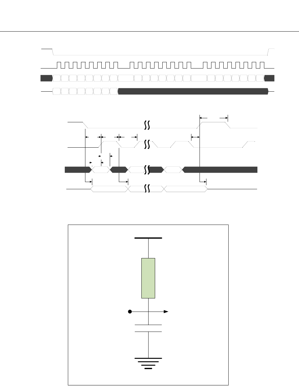
Figure 24. SPI write operation
Figure 25. SPI NOP timing diagram
Figure 26. Rpull and Cload
C7 C6 C5 C4 C3 C2 C1 C0 D7 D6 D5 D4 D3 D2 D1 D0 D15 D14 D13 D12 D11 D10 D9 D8
S7 S6 S5 S4 S3 S2 S1 S0
CSN
SCK
MO S I
MISO
C7 C6 C0
S7 S0
TcdzTcdTcsd
Tdh
Tdc
TcchTclTclTchTcc Tch
TcwhTcwh
CSN
SCK
MOSI
MISO
Vdd
Rpull
Cload
ExternalPin of nRF24L01

Table 18. SPI timing parameters (Cload = 5pF)
Table 19. SPI timing parameters (Cload = 10pF)
Table 20. SPI timing parameters (Rpull = 10k
Ω
, Cload = 50pF)
Symbol Parameters Min Max Units
Tdc Data to SCK Setup 2 ns
Tdh SCK to Data Hold 2 ns
Tcsd CSN to Data Valid 38 ns
Tcd SCK to Data Valid 55 ns
Tcl SCK Low Time 40 ns
Tch SCK High Time 40 ns
Fsck SCK Frequency 0 8 MHz
Tr,Tf SCK Rise and Fall 100 ns
Tcc CSN to SCK Setup 2 ns
Tcch SCK to CSN Hold 2 ns
Tc w h CSN Inactive time 50 ns
Tcd z CSN to Output High Z 38 ns
Symbol Parameters Min Max Units
Tdc Data to SCK Setup 2 ns
Tdh SCK to Data Hold 2 ns
Tcsd CSN to Data Valid 42 ns
Tcd SCK to Data Valid 58 ns
Tcl SCK Low Time 40 ns
Tch SCK High Time 40 ns
Fsck SCK Frequency 0 8 MHz
Tr,Tf SCK Rise and Fall 100 ns
Tcc CSN to SCK Setup 2 ns
Tcch SCK to CSN Hold 2 ns
Tc w h CSN Inactive time 50 ns
Tcd z CSN to Output High Z 42 ns
Symbol Parameters Min Max Units
Tdc Data to SCK Setup 2 ns
Tdh SCK to Data Hold 2 ns
Tcsd CSN to Data Valid 75 ns
Tcd SCK to Data Valid 86 ns
Tcl SCK Low Time 40 ns
Tch SCK High Time 40 ns
Fsck SCK Frequency 0 5 MHz
Tr,Tf SCK Rise and Fall 100 ns
Tcc CSN to SCK Setup 2 ns
Tcch SCK to CSN Hold 2 ns
Tc w h CSN Inactive time 50 ns
Tcd z CSN to Output High Z 75 ns

Table 21. SPI timing parameters (Rpull = 10k
Ω
, Cload = 100pF)
Table 22. SPI timing parameters (Rpull = 50k
Ω
, Cload = 50pF)
Table 23. SPI timing parameters (Rpull = 50k
Ω
, Cload = 100pF)
Symbol Parameters Min Max Units
Tdc Data to SCK Setup 2 ns
Tdh SCK to Data Hold 2 ns
Tcsd CSN to Data Valid 116 ns
Tcd SCK to Data Valid 123 ns
Tcl SCK Low Time 40 ns
Tch SCK High Time 40 ns
Fsck SCK Frequency 0 4 MHz
Tr,Tf SCK Rise and Fall 100 ns
Tcc CSN to SCK Setup 2 ns
Tcch SCK to CSN Hold 2 ns
Tc w h CSN Inactive time 50 ns
Tcd z CSN to Output High Z 116 ns
Symbol Parameters Min Max Units
Tdc Data to SCK Setup 2 ns
Tdh SCK to Data Hold 2 ns
Tcsd CSN to Data Valid 75 ns
Tcd SCK to Data Valid 85 ns
Tcl SCK Low Time 40 ns
Tch SCK High Time 40 ns
Fsck SCK Frequency 0 5 MHz
Tr,Tf SCK Rise and Fall 100 ns
Tcc CSN to SCK Setup 2 ns
Tcch SCK to CSN Hold 2 ns
Tc w h CSN Inactive time 50 ns
Tcd z CSN to Output High Z 75 ns
Symbol Parameters Min Max Units
Tdc Data to SCK Setup 2 ns
Tdh SCK to Data Hold 2 ns
Tcsd CSN to Data Valid 116 ns
Tcd SCK to Data Valid 121 ns
Tcl SCK Low Time 40 ns
Tch SCK High Time 40 ns
Fsck SCK Frequency 0 4 MHz
Tr,Tf SCK Rise and Fall 100 ns
Tcc CSN to SCK Setup 2 ns
Tcch SCK to CSN Hold 2 ns
Tc w h CSN Inactive time 50 ns
Tcd z CSN to Output High Z 116 ns
Data FIFO
The data FIFOs are used to store payload that is transmitted (TX FIFO) or payload that is received and
ready to be clocked out (RX FIFO). The FIFOs are accessible in both PTX mode and PRX mode.
The following FIFOs are present in nRF24L01:
• TX three level, 32 byte FIFO
• RX three level, 32 byte FIFO
Both FIFOs have a controller and are accessible through the SPI by using dedicated SPI commands. A TX
FIFO in PRX can store payload for ACK packets to three different PTX devices. If the TX FIFO contains
more than one payload to a pipe, payloads are handled using the first in - first out principle. The TX FIFO in
a PRX is blocked if all pending payloads are addressed to pipes where the link to the PTX is lost. In this
case, the MCU can flush the TX FIFO by using the FLUSH_TX command.
The RX FIFO in PRX may contain payload from up to three different PTX devices.
A TX FIFO in PTX can have up to three payloads stored.
The TX FIFO can be written to by three commands, W_TX_PAYLOAD and W_TX_PAYLOAD_NO_ACK in PTX
mode and W_ACK_PAYLOAD in PRX mode. All three commands give access to the TX_PLD register.
The RX FIFO can be read by the command R_RX_PAYLOAD in both PTX and PRX mode. This command
gives access to the RX_PLD register.
The payload in TX FIFO in a PTX is NOT removed if the MAX_RT IRQ is asserted. Figure 27. is a block dia-
gram of the TX FIFO and the RX FIFO.
Figure 27. FIFO block diagram
In the FIFO_STATUS register it is possible to read if the TX and RX FIFO is full or empty. The TX_REUSE
bit is also available in the FIFO_STATUS register. TX_REUSE is set by the SPI command REUSE_TX_PL,
and is reset by the SPI commands W_TX_PAYLOAD or FLUSH TX.
Data
TX FIFO
32 byte
32 byte
32 byte
TX FIFO Controller
Data
Control
SPI
command
decoder
RX FIFO
32 byte
32 byte
32 byte
RX FIFO Controller
Data Data
Control
SPI

Interrupt
The nRF24L01 has an active low interrupt (IRQ) pin. The IRQ pin is activated when TX_DS IRQ, RX_DR
IRQ or MAX_RT IRQ are set high by the state machine in the STATUS register. The IRQ pin resets when
MCU writes '1' to the IRQ source bit in the STATUS register. The IRQ mask in the CONFIG register is used
to select the IRQ sources that are allowed to assert the IRQ pin. By setting one of the MASK bits high, the
corresponding IRQ source is disabled. By default all IRQ sources are enabled.
Note: The 3 bit pipe information in the STATUS register is updated during the IRQ pin high to low
transition. If the STATUS register is read during an IRQ pin high to low transition, the pipe
information is unreliable.

Register Map
You can configure and control the radio chip by accessing the register map through the SPI by using read
and write commands.
Register map table
All undefined bits in the table below are redundant. They are read out as '0'.
Note: Addresses 18 to 1B are reserved for test purposes, altering them will make the chip malfunc-
tion.
Address
(Hex) Mnemonic Bit Reset
Value Type Description
00 CONFIG Configuration Register
Reserved 7 0 R/W Only '0' allowed
MASK_RX_DR 6 0 R/W Mask interrupt caused by RX_DR
1: Interrupt not reflected on the IRQ pin
0: Reflect RX_DR as active low interrupt on the
IRQ pin
MASK_TX_DS 5 0 R/W Mask interrupt caused by TX_DS
1: Interrupt not reflected on the IRQ pin
0: Reflect TX_DS as active low interrupt on the
IRQ pin
MASK_MAX_RT 4 0 R/W Mask interrupt caused by MAX_RT
1: Interrupt not reflected on the IRQ pin
0: Reflect MAX_RT as active low interrupt on the
IRQ pin
EN_CRC 3 1 R/W Enable CRC. Forced high if one of the bits in
the EN_AA is high
CRCO 2 0 R/W CRC encoding scheme
'0' - 1 byte
'1' – 2 bytes
PWR_UP 1 0 R/W 1: POWER UP, 0:POWER DOWN
PRIM_RX 0 0 R/W RX/TX control
1: PRX, 0: PTX
01 EN_AA
Enhanced
ShockBurst™
Enable ‘Auto Acknowledgment’ Function Dis-
able this functionality to be compatible with
nRF2401, see page 65
Reserved 7:6 00 R/W Only '00' allowed
ENAA_P5 5 1 R/W Enable auto acknowledgement data pipe 5
ENAA_P4 4 1 R/W Enable auto acknowledgement data pipe 4
ENAA_P3 3 1 R/W Enable auto acknowledgement data pipe 3
ENAA_P2 2 1 R/W Enable auto acknowledgement data pipe 2
ENAA_P1 1 1 R/W Enable auto acknowledgement data pipe 1
ENAA_P0 0 1 R/W Enable auto acknowledgement data pipe 0
02 EN_RXADDR Enabled RX Addresses
Reserved 7:6 00 R/W Only '00' allowed
ERX_P5 5 0 R/W Enable data pipe 5.
ERX_P4 4 0 R/W Enable data pipe 4.

ERX_P3 3 0 R/W Enable data pipe 3.
ERX_P2 2 0 R/W Enable data pipe 2.
ERX_P1 1 1 R/W Enable data pipe 1.
ERX_P0 0 1 R/W Enable data pipe 0.
03 SETUP_AW Setup of Address Widths
(common for all data pipes)
Reserved 7:2 000000 R/W Only '000000' allowed
AW 1:0 11 R/W RX/TX Address field width
'00' - Illegal
'01' - 3 bytes
'10' - 4 bytes
'11' – 5 bytes
LSByte is used if address width is below 5 bytes
04 SETUP_RETR Setup of Automatic Retransmission
ARD 7:4 0000 R/W Auto Retransmit Delay
‘0000’ – Wait 250µS
‘0001’ – Wait 500µS
‘0010’ – Wait 750µS
……..
‘1111’ – Wait 4000µS
(Delay defined from end of transmission to start
of next transmission)a
ARC 3:0 0011 R/W Auto Retransmit Count
‘0000’ –Re-Transmit disabled
‘0001’ – Up to 1 Re-Transmit on fail of AA
……
‘1111’ – Up to 15 Re-Transmit on fail of AA
05 RF_CH RF Channel
Reserved 7 0 R/W Only '0' allowed
RF_CH 6:0 0000010 R/W Sets the frequency channel nRF24L01 operates
on
06 RF_SETUP RF Setup Register
Reserved 7:5 000 R/W Only '000' allowed
PLL_LOCK 4 0 R/W Force PLL lock signal. Only used in test
RF_DR 3 1 R/W Air Data Rate
‘0’ – 1Mbps
‘1’ – 2Mbps
RF_PWR 2:1 11 R/W Set RF output power in TX mode
'00' – -18dBm
'01' – -12dBm
'10' – -6dBm
'11' – 0dBm
LNA_HCURR 0 1 R/W Setup LNA gain
Address
(Hex) Mnemonic Bit Reset
Value Type Description

07 STATUS Status Register (In parallel to the SPI command
word applied on the MOSI pin, the STATUS reg-
ister is shifted serially out on the MISO pin)
Reserved 7 0 R/W Only '0' allowed
RX_DR 6 0 R/W Data Ready RX FIFO interrupt. Asserted when
new data arrives RX FIFOb.
Write 1 to clear bit.
TX_DS 5 0 R/W Data Sent TX FIFO interrupt. Asserted when
packet transmitted on TX. If AUTO_ACK is acti-
vated, this bit is set high only when ACK is
received.
Write 1 to clear bit.
MAX_RT 4 0 R/W Maximum number of TX retransmits interrupt
Write 1 to clear bit. If MAX_RT is asserted it must
be cleared to enable further communication.
RX_P_NO 3:1 111 R Data pipe number for the payload available for
reading from RX_FIFO
000-101: Data Pipe Number
110: Not Used
111: RX FIFO Empty
TX_FULL 0 0 R TX FIFO full flag.
1: TX FIFO full.
0: Available locations in TX FIFO.
08 OBSERVE_TX Transmit observe register
PLOS_CNT 7:4 0 R Count lost packets. The counter is overflow pro-
tected to 15, and discontinues at max until
reset. The counter is reset by writing to RF_CH.
See page 65 and page 74.
ARC_CNT 3:0 0 R Count retransmitted packets. The counter is
reset when transmission of a new packet starts.
See page 65.
09 CD
Reserved 7:1 000000 R
CD 0 0 R Carrier Detect. See page page 74.
0A RX_ADDR_P0 39:0 0xE7E7E
7E7E7
R/W Receive address data pipe 0. 5 Bytes maximum
length. (LSByte is written first. Write the number
of bytes defined by SETUP_AW)
0B RX_ADDR_P1 39:0 0xC2C2C
2C2C2
R/W Receive address data pipe 1. 5 Bytes maximum
length. (LSByte is written first. Write the number
of bytes defined by SETUP_AW)
0C RX_ADDR_P2 7:0 0xC3 R/W Receive address data pipe 2. Only LSB. MSBy-
tes is equal to RX_ADDR_P1[39:8]
0D RX_ADDR_P3 7:0 0xC4 R/W Receive address data pipe 3. Only LSB. MSBy-
tes is equal to RX_ADDR_P1[39:8]
0E RX_ADDR_P4 7:0 0xC5 R/W Receive address data pipe 4. Only LSB. MSBy-
tes is equal to RX_ADDR_P1[39:8]
0F RX_ADDR_P5 7:0 0xC6 R/W Receive address data pipe 5. Only LSB. MSBy-
tes is equal to RX_ADDR_P1[39:8]
Address
(Hex) Mnemonic Bit Reset
Value Type Description

10 TX_ADDR 39:0 0xE7E7E
7E7E7
R/W Transmit address. Used for a PTX device only.
(LSByte is written first)
Set RX_ADDR_P0 equal to this address to han-
dle automatic acknowledge if this is a PTX
device with Enhanced ShockBurst™ enabled.
See page 65.
11 RX_PW_P0
Reserved 7:6 00 R/W Only '00' allowed
RX_PW_P0 5:0 0 R/W Number of bytes in RX payload in data pipe 0 (1
to 32 bytes).
0 Pipe not used
1 = 1 byte
…
32 = 32 bytes
12 RX_PW_P1
Reserved 7:6 00 R/W Only '00' allowed
RX_PW_P1 5:0 0 R/W Number of bytes in RX payload in data pipe 1 (1
to 32 bytes).
0 Pipe not used
1 = 1 byte
…
32 = 32 bytes
13 RX_PW_P2
Reserved 7:6 00 R/W Only '00' allowed
RX_PW_P2 5:0 0 R/W Number of bytes in RX payload in data pipe 2 (1
to 32 bytes).
0 Pipe not used
1 = 1 byte
…
32 = 32 bytes
14 RX_PW_P3
Reserved 7:6 00 R/W Only '00' allowed
RX_PW_P3 5:0 0 R/W Number of bytes in RX payload in data pipe 3 (1
to 32 bytes).
0 Pipe not used
1 = 1 byte
…
32 = 32 bytes
15 RX_PW_P4
Reserved 7:6 00 R/W Only '00' allowed
Address
(Hex) Mnemonic Bit Reset
Value Type Description

RX_PW_P4 5:0 0 R/W Number of bytes in RX payload in data pipe 4 (1
to 32 bytes).
0 Pipe not used
1 = 1 byte
…
32 = 32 bytes
16 RX_PW_P5
Reserved 7:6 00 R/W Only '00' allowed
RX_PW_P5 5:0 0 R/W Number of bytes in RX payload in data pipe 5 (1
to 32 bytes).
0 Pipe not used
1 = 1 byte
…
32 = 32 bytes
17 FIFO_STATUS FIFO Status Register
Reserved 7 0 R/W Only '0' allowed
TX_REUSE 6 0 R Reuse last transmitted data packet if set high.
The packet is repeatedly retransmitted as long
as CE is high. TX_REUSE is set by the SPI com-
mand REUSE_TX_PL, and is reset by the SPI
commands W_TX_PAYLOAD or FLUSH TX
TX_FULL 5 0 R TX FIFO full flag. 1: TX FIFO full. 0: Available
locations in TX FIFO.
TX_EMPTY 4 1 R TX FIFO empty flag.
1: TX FIFO empty.
0: Data in TX FIFO.
Reserved 3:2 00 R/W Only '00' allowed
RX_FULL 1 0 R RX FIFO full flag.
1: RX FIFO full.
0: Available locations in RX FIFO.
RX_EMPTY 0 1 R RX FIFO empty flag.
1: RX FIFO empty.
0: Data in RX FIFO.
N/A ACK_PLDc255:0 X W Written by separate SPI command
ACK packet payload to data pipe number PPP
given in SPI command
Used in RX mode only
Maximum three ACK packet payloads can be
pending. Payloads with same PPP are handled
first in first out.
N/A TX_PLD 255:0 X W Written by separate SPI command TX data pay-
load register 1 - 32 bytes.
This register is implemented as a FIFO with
three levels.
Used in TX mode only
Address
(Hex) Mnemonic Bit Reset
Value Type Description
Table 24. Register map of nRF24L01
N/A RX_PLD 255:0 X R Read by separate SPI command
RX data payload register. 1 - 32 bytes.
This register is implemented as a FIFO with
three levels.
All RX channels share the same FIFO
1C DYNPDcEnable dynamic payload length
Reserved 7:6 0 R/W Only ‘00’ allowed
DPL_P5 5 0 R/W Enable dyn. payload length data pipe 5.
(Requires EN_DPL and ENAA_P5)
DPL_P4 4 0 R/W Enable dyn. payload length data pipe 4.
(Requires EN_DPL and ENAA_P4)
DPL_P3 3 0 R/W Enable dyn. payload length data pipe 3.
(Requires EN_DPL and ENAA_P3)
DPL_P2 2 0 R/W Enable dyn. payload length data pipe 2.
(Requires EN_DPL and ENAA_P2)
DPL_P1 1 0 R/W Enable dyn. payload length data pipe 1.
(Requires EN_DPL and ENAA_P1)
DPL_P0 0 0 R/W Enable dyn. payload length data pipe 0.
(Requires EN_DPL and ENAA_P0)
1D FEATUREcR/W Feature Register
Reserved 7:3 0 R/W Only ‘00000’ allowed
EN_DPL 2 0 R/W Enables Dynamic Payload Length
EN_ACK_PAYd1 0 R/W Enables Payload with ACK
EN_DYN_ACK 0 0 R/W Enables the W_TX_PAYLOAD_NOACK command
a. This is the time the PTX is waiting for an ACK packet before a retransmit is made. The PTX is in RX mode
for a minimum of 250µS, but it stays in RX mode to the end of the packet if that is longer than 250µS. Then
it goes to standby-I mode for the rest of the specified ARD. After the ARD it goes to TX mode and then
retransmits the packet.
b. The RX_DR IRQ is asserted by a new packet arrival event. The procedure for handling this interrupt
should be: 1) read payload through SPI, 2) clear RX_DR IRQ, 3) read FIFO_STATUS to check if there
are more payloads available in RX FIFO, 4) if there are more data in RX FIFO, repeat from 1)
c. To activate this feature use the ACTIVATE SPI command followed by data 0x73. The corresponding bits
in the FEATURE register must be set.
d. If ACK packet payload is activated, ACK packets have dynamic payload lengths and the Dynamic Pay-
load Length feature should be enabled for pipe 0 on the PTX and PRX. This is to ensure that they receive
the ACK packets with payloads. If the payload in ACK is more than 15 byte in 2Mbps mode the ARD must
be 500µS or more, and if the payload is more than 5byte in 1Mbps mode the ARD must be 500µS or more.
Address
(Hex) Mnemonic Bit Reset
Value Type Description

Appendix A - Enhanced ShockBurst™ - Configuration and Communi-
cation Example
Enhanced ShockBurst™ Transmitting Payload
1. The configuration bit PRIM_RX has to be low.
2. When the application MCU has data to transmit, the address for the receiving node (TX_ADDR)
and payload data (TX_PLD) has to be clocked into nRF24L01 through the SPI. The width of TX-
payload is counted from number of bytes written into the TX FIFO from the MCU. TX_PLD must
be written continuously while holding CSN low. TX_ADDR does not have to be rewritten if it is
unchanged from last transmit. If the PTX device shall receive acknowledge, data pipe 0 has to be
configured to receive the ACK packet. The RX address for data pipe 0 (RX_ADDR_P0) has to be
equal to the TX address (TX_ADDR) in the PTX device. For the example in Figure 12. on page 37
the following address settings have to be performed for the TX5 device and the RX device:
TX5 device: TX_ADDR = 0xB3B4B5B605
TX5 device: RX_ADDR_P0 = 0xB3B4B5B605
RX device: RX_ADDR_P5 = 0xB3B4B5B605
3. A high pulse on CE starts the transmission. The minimum pulse width on CE is 10µs.
4. nRF24L01 ShockBurst™:
XRadio is powered up.
X16MHz internal clock is started.
XRF packet is completed (see the packet description).
XData is transmitted at high speed (1Mbps or 2Mbps configured by MCU).
5. If auto acknowledgement is activated (ENAA_P0=1) the radio goes into RX mode immediately,
unless the NO_ACK bit is set in the received packet. If a valid packet has been received in the
valid acknowledgement time window, the transmission is considered a success. The TX_DS bit in
the STATUS register is set high and the payload is removed from TX FIFO. If a valid ACK packet
is not received in the specified time window, the payload is retransmitted (if auto retransmit is
enabled). If the auto retransmit counter (ARC_CNT) exceeds the programmed maximum limit
(ARC), the MAX_RT bit in the STATUS register is set high. The payload in TX FIFO is NOT
removed. The IRQ pin is active when MAX_RT or TX_DS is high. To turn off the IRQ pin, the inter-
rupt source must be reset by writing to the STATUS register (see Interrupt chapter). If no ACK
packet is received for a packet after the maximum number of retransmits, no further packets can
be transmitted before the MAX_RT interrupt is cleared. The packet loss counter (PLOS_CNT) is
incremented at each MAX_RT interrupt. That is, ARC_CNT counts the number of retransmits that
was required to get a single packet through. PLOS_CNT counts the number of packets that did not
get through after maximum number of retransmits.
6. nRF24L01 goes into standby-I mode if CE is low. Otherwise next payload in TX FIFO is transmit-
ted. If TX FIFO is empty and CE is still high, nRF24L01 enters standby-II mode.
7. If nRF24L01 is in standby-II mode, it goes to standby-I mode immediately if CE is set low.
Enhanced ShockBurst™ Receive Payload
1. RX is selected by setting the PRIM_RX bit in the CONFIG register to high. All data pipes that
receive data must be enabled (EN_RXADDR register), auto acknowledgement for all pipes running
Enhanced ShockBurst™ has to be enabled (EN_AA register), and the correct payload widths
must be set (RX_PW_Px registers). Addresses have to be set up as described in item 2 in the
Enhanced ShockBurst™ transmit payload chapter above.
2. Active RX mode is started by setting CE high.
3. After 130µs nRF24L01 is monitoring the air for incoming communication.
4. When a valid packet has been received (matching address and correct CRC), the payload is
stored in the RX-FIFO, and the RX_DR bit in STATUS register is set high. The IRQ pin is active

when RX_DR is high. RX_P_NO in STATUS register indicates what data pipe the payload has been
received in.
5. If auto acknowledgement is enabled, an ACK packet is transmitted back, unless the NO_ACK bit
is set in the received packet. If there is a payload in the TX_PLD FIFO, this payload is added to
the ACK packet.
6. MCU sets the CE pin low to enter standby-I mode (low current mode).
7. MCU can clock out the payload data at a suitable rate through the SPI.
8. nRF24L01 is now ready for entering TX or RX mode or power down mode.

Appendix B - Configuration for compatibility with nRF24XX
How to setup nRF24L01 to receive from an nRF2401/nRF2402/nRF24E1/nRF24E2:
1. Use the same CRC configuration as the nRF2401/nRF2402/nRF24E1/nRF24E2
2. Set the PWR_UP and PRIM_RX bit to 1
3. Disable auto acknowledgement on the data pipe that is addressed
4. Use the same address width as the PTX device
5. Use the same frequency channel as the PTX device
6. Select data rate 1Mbps on both nRF24L01 and nRF2401/nRF2402/nRF24E1/nRF24E2
7. Set correct payload width on the data pipe that is addressed
8. Set CE high
How to setup nRF24L01 to transmit to an nRF2401/nRF24E1:
1. Use the same CRC configuration as the nRF2401/nRF2402/nRF24E1/nRF24E2
2. Set the PRIM_RX bit to 0
3. Set the Auto Retransmit Count to 0 to disable the auto retransmit functionality
4. Use the same address width as the nRF2401/nRF2402/nRF24E1/nRF24E2 uses
5. Use the same frequency channel as the nRF2401/nRF2402/nRF24E1/nRF24E2 uses
6. Select data rate 1Mbps on both nRF24L01 and nRF2401/nRF2402/nRF24E1/nRF24E2
7. Set PWR_UP high
8. Clock in a payload that has the same length as the nRF2401/nRF2402/nRF24E1/nRF24E2 is
configured to receive
9. Pulse CE to transmit the packet

Appendix C - Carrier wave output power
The output power of a radio is a critical factor for achieving wanted range. Output power is also the first test
criteria needed to qualify for all telecommunication regulations.
Configuration
1. Set PWR_UP = 1 in the CONFIG register
2. Wait 1.5ms PWR_UP->standby
3. Clear the PRIM_RX in the CONFIG register
4. Set all auto acknowledgement functionality in the EN_AA register and the SETUP_RETR register
to 0
5. Set output power
6. Set PLL_LOCK to 1
7. Configure TX address as 5 bytes with all 0xFF
8. Fill the TX payload with 32 bytes of 0xFF
9. Turn off CRC
10. Set the wanted RF channel
11. Transmit the packet by pulsing CE (minimum 10µs)
12. Wait until the transmission ends (indicated by IRQ going active, a fixed delay of 1ms can also be
used)
13. Set CE high
14. Use the SPI command for re-use of last sent packet (REUSE_TX_PL)
15. Keep CE high as long as the carrier is needed
The nRF24L01 should now output a carrier.
Note: This is not a clean carrier but is slightly modulated by the preamble.
Hosted Information
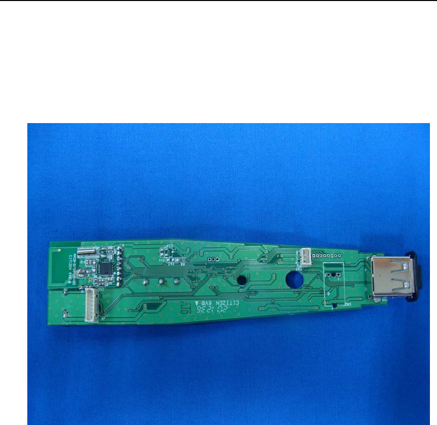
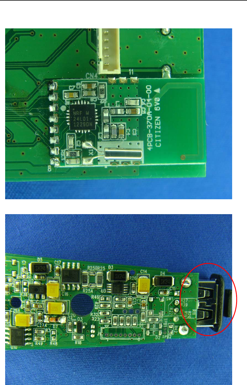
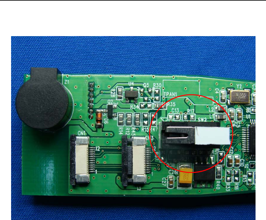
The “KC-52002B” is a test-hosted board for NUMA’s “2.4G NRM” RF module.
The hosted board manufacture and model name is NUMA Electronics Inc. /
KC-52002B
The board is equipped barcode scanner and USB function. The hosted doesn’t
have any from metal shielded.
1. Hardware Setup
The RF module need to soldered on the test-hosted board.
The test-hosted board power by USB (DC 5V).
Before into the test mode need to press a button and plug-in
the USB to PC or Notebook PC.