NXP Austria OM5569-NT322E NTAG I2C plus Explorer Kit User Manual Integration Manual EXPLORE NFC
NXP Austria GmbH NTAG I2C plus Explorer Kit Integration Manual EXPLORE NFC
UserManual.wiki
>
NXP Austria
>
OM5569 NT322E User Manual
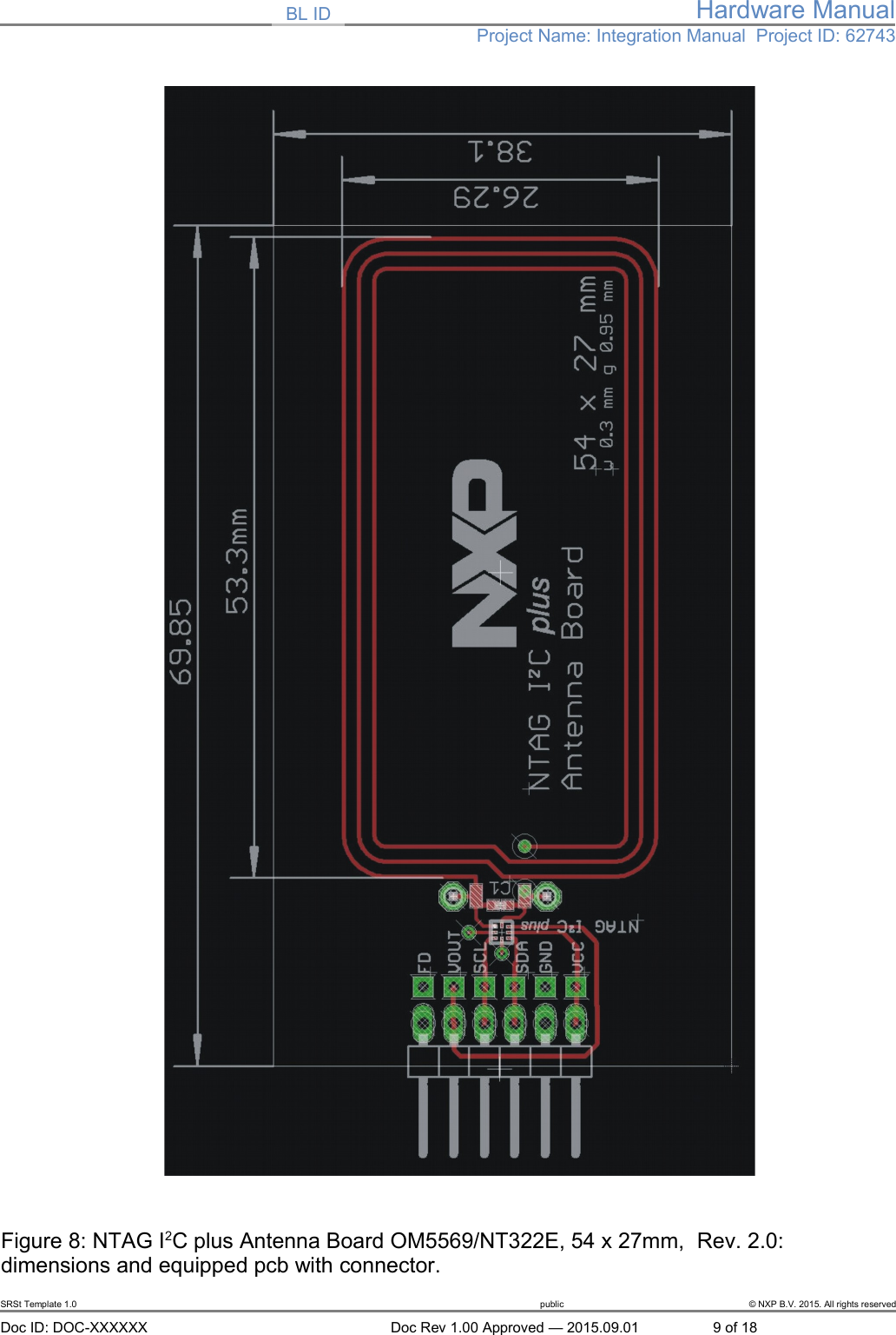
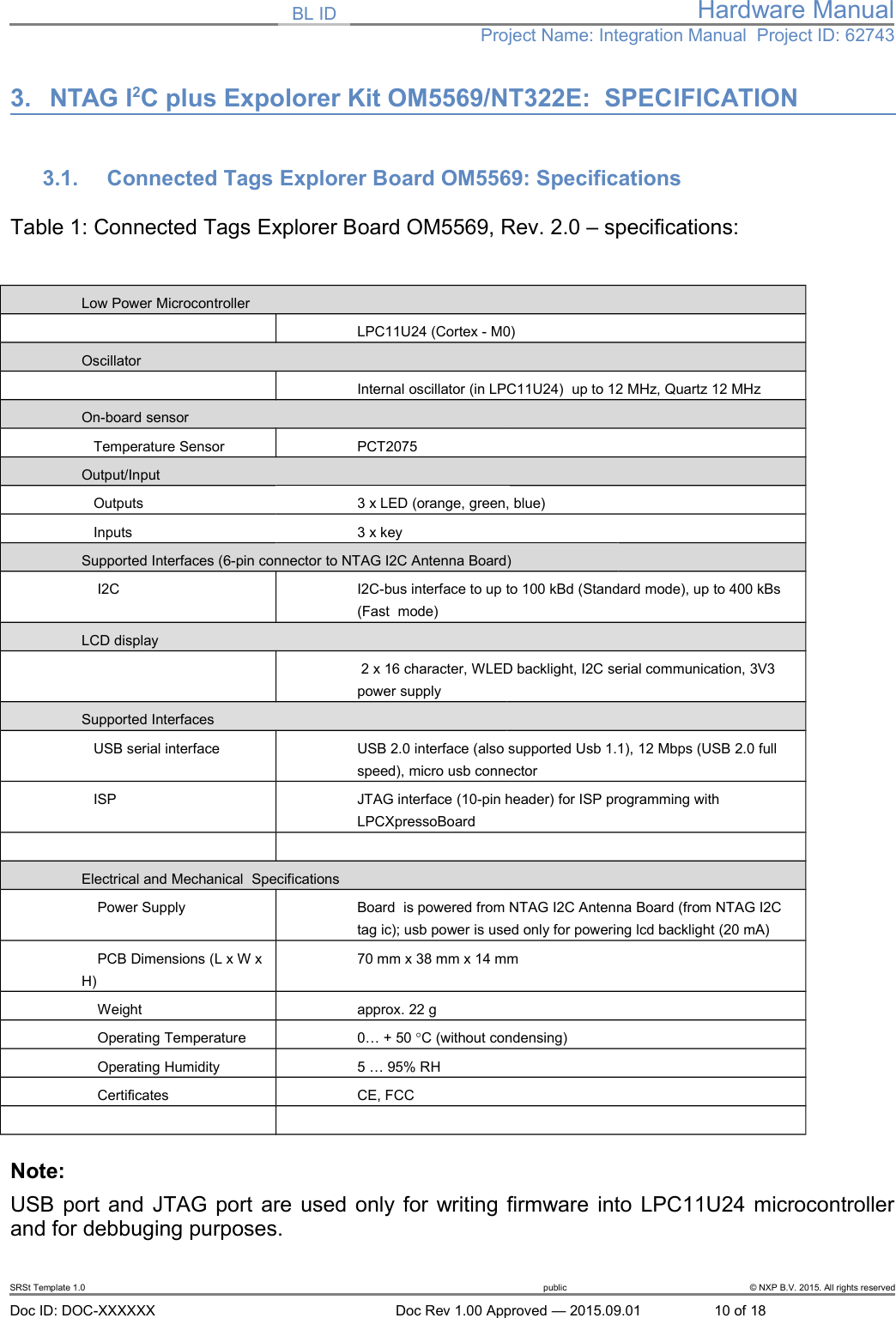
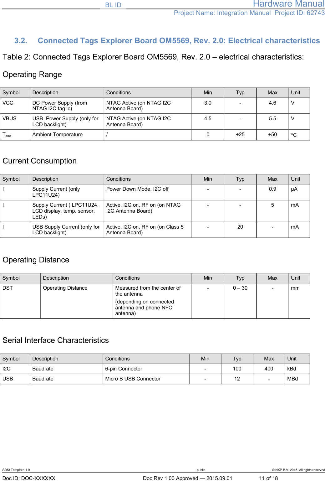
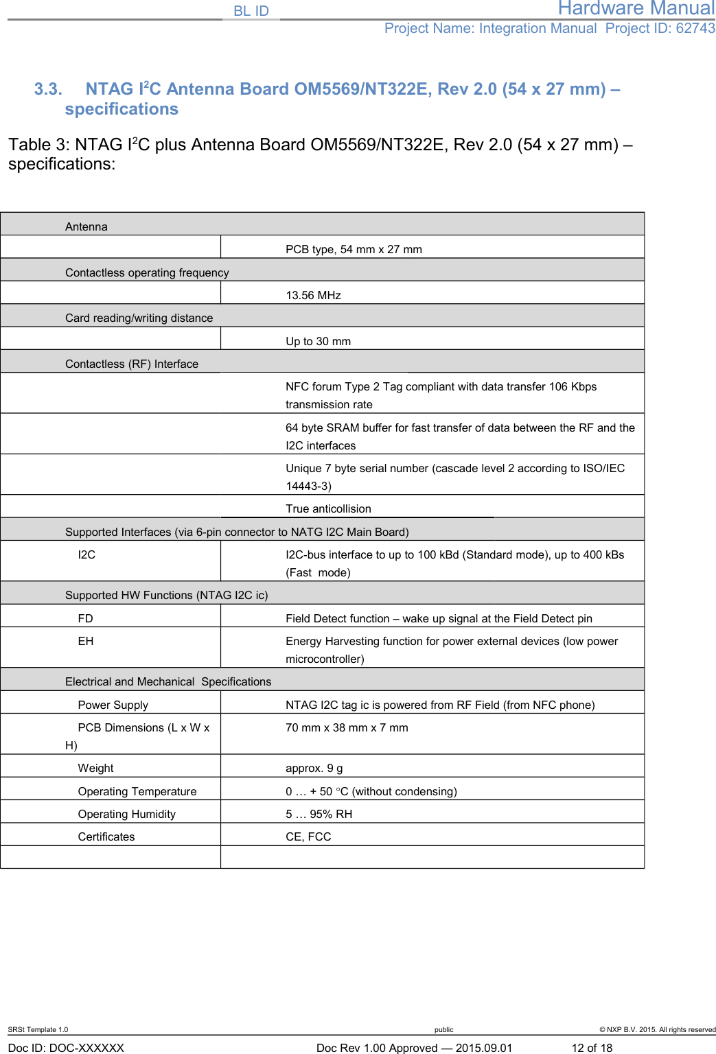
Hardware Manual
Navigation menu
Upload a User Manual
Namespaces
Wiki Guide
HTML
PDF
Info
Views
User Manual
Discussion / Help
Navigation