NXP Austria OM5569-NT322E NTAG I2C plus Explorer Kit User Manual Integration Manual EXPLORE NFC
NXP Austria GmbH NTAG I2C plus Explorer Kit Integration Manual EXPLORE NFC
Hardware Manual

Document information
Info Content
Author Pavel Slamnik
Author Role Design Engineer
Keywords NTAG I2C plus Explorer Kit OM5569-NT322E, RFID, NFC, TAG, NTAG
Hardware Manual: NTAG I2C plus Explorer
Kit OM5569/NT322E
Doc Rev 1.00 Approved — 2015.09.01 BL ID

BL ID Hardware Manual
Project Name: Integration Manual Project ID: 62743
Revision History
Revision Date Description Author
1.01 2015.12.07 First Version Pavel Slamnik
Copyright: @2009, NXP Semiconductors
The information contained herein is the exclusive and confidential property of NXP Semiconductors and, except as
otherwise indicated, shall not be disclosed or reproduced in whole or in part.
SRS Template_vs 1.0 public © NXP B.V. 2015. All rights reserved
Doc ID: DOC-XXXXXX Doc Rev 1.00 Approved — 2015.09.01 2 of 18
BL ID Hardware Manual
Project Name: Integration Manual Project ID: 62743
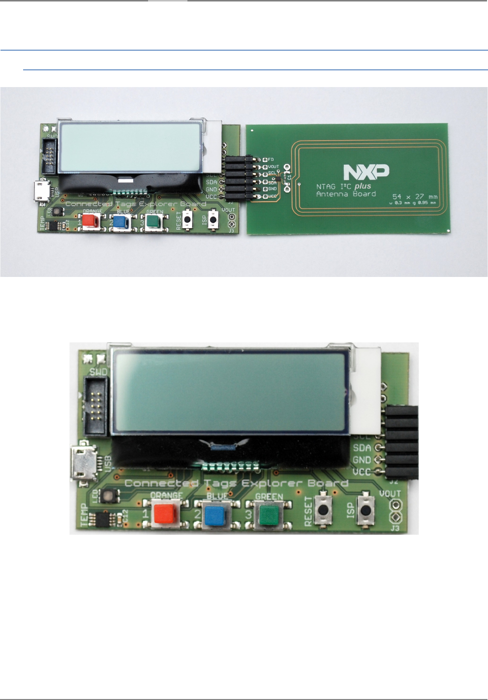
1. NTAG I2C plus Explorer Kit OM5569/NT322E: Photo
Figure 1: NTAG I2C plus Explorer Kit OM5569/NT322E – Connected Tags Explorer Board
with NTAG I2C plus Antenna Board 54 x 27mm (pcb type).
Figure 2: Connected Tags Explorer Board OM5569, Rev 2.0.
SRSt Template 1.0 public © NXP B.V. 2015. All rights reserved
Doc ID: DOC-XXXXXX Doc Rev 1.00 Approved — 2015.09.01 3 of 18
BL ID Hardware Manual
Project Name: Integration Manual Project ID: 62743
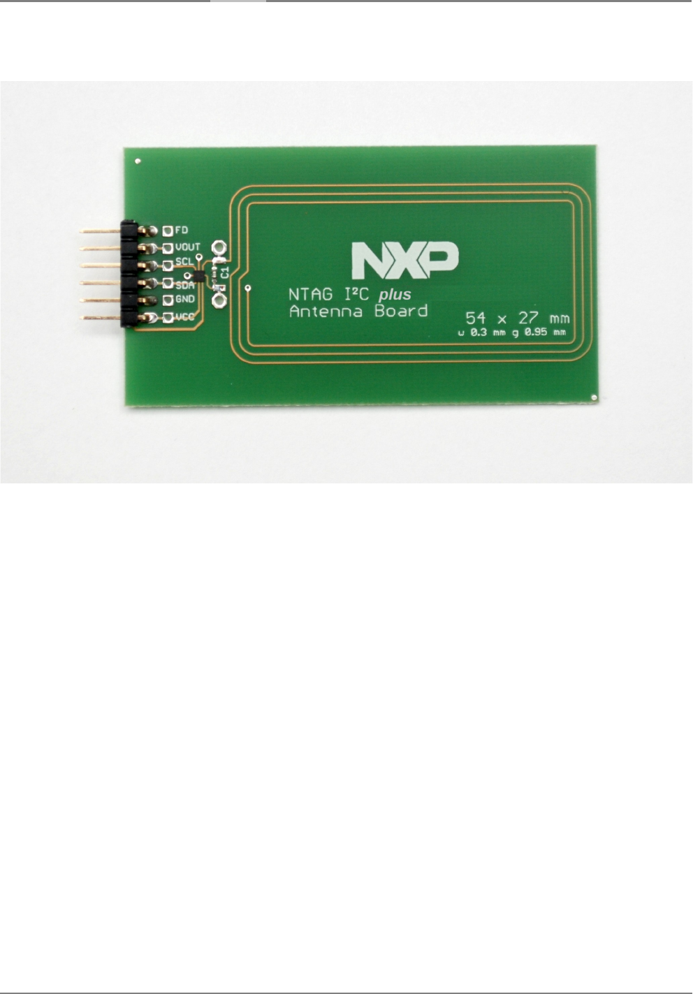
Figure 3: NTAG I2C plus Antenna Board OM5569/NT322E, 54 x 27 mm.
SRSt Template 1.0 public © NXP B.V. 2015. All rights reserved
Doc ID: DOC-XXXXXX Doc Rev 1.00 Approved — 2015.09.01 4 of 18

BL ID Hardware Manual
Project Name: Integration Manual Project ID: 62743
2. NTAG I2C plus Explorer Kit OM5569/NT322E: Description
2.1. Operational desription
To demonstrate the unique properties of the NTAG I2C tag chip, NXP developed the NTAG
I2C plus Explorer Kit OM5569/NT322E which consists from Connected Tags Explorer Board
OM5569 and one NTAG I2C plus Antenna Board OM5569/NT322E (54 x 27 mm ).
NXP’s NTAG I2C plus Explorer Kit is an all-in-one demonstration/development resource for
NFC connected tags. Designed to emulate using an NTAG I2C tag chip in an embedded
electronic system, the kit centers around a multi-purpose microprocessor-based
development/Explorer board, and includes a full complement of hardware and software tools
to support investigation of the NTAG I2C chip operation, the NFC RF communication link,
and the I2C serial bus connected link; perform a variety of demonstrations; and develop/test
your own applications.
NTAG I2C tag chips mounted on a variety of different antenna types (FR4 PCB-based with
separate antenna pads for custom antenna use, as well as a Flex antenna board based for
easier product insertion testing) and with built-in I2C serial bus interface connectors.
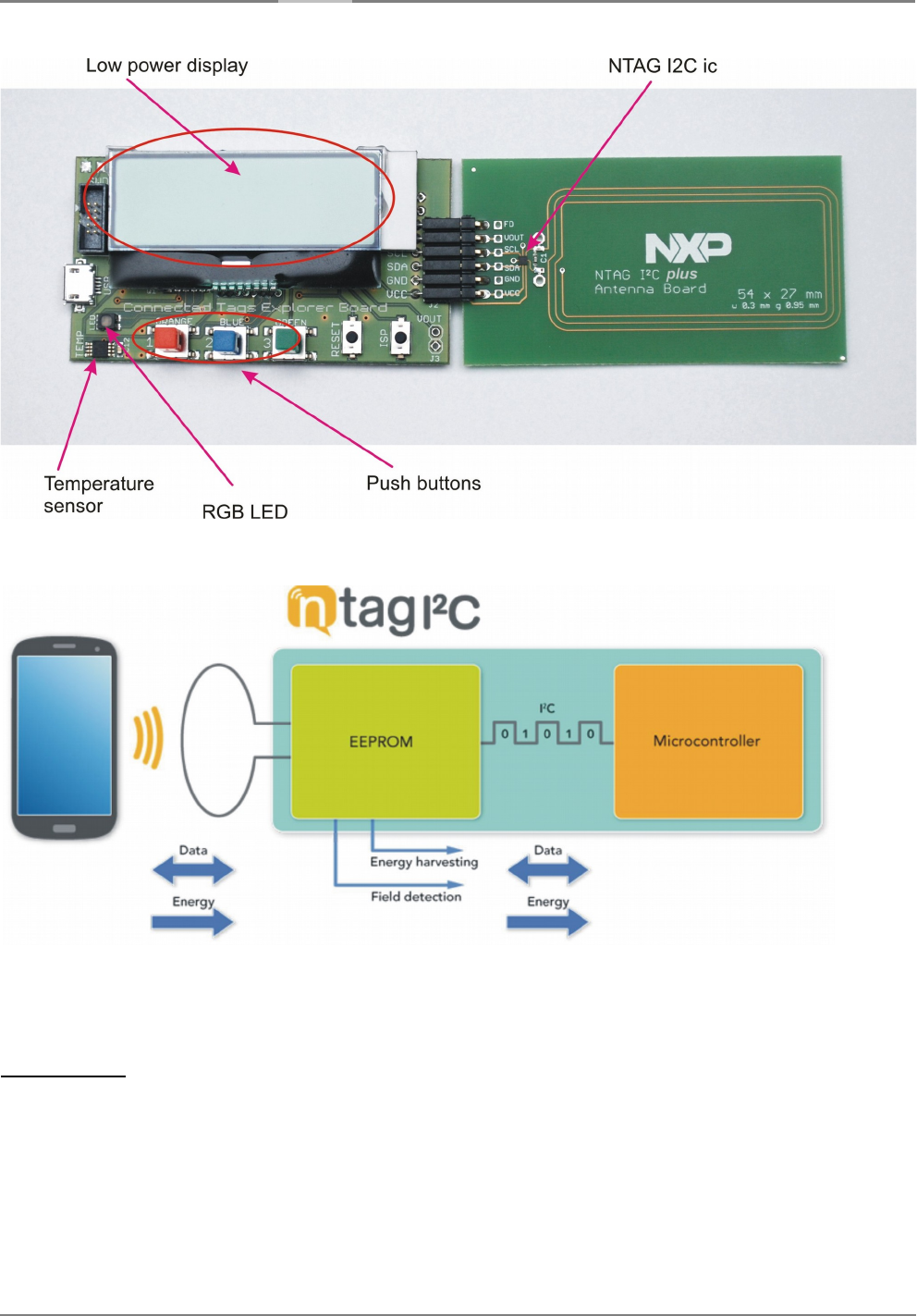
The Connected Tags Explorer board contains an NXP microcontroller (LPC11U24 Cortex-
M0), a RGB (red - green - blue) LED and OBG (orange – blue – green) push button as well
as an NXP temperature sensor (PCT 2075) and an LCD screen to show the messages
coming from the NTAG and the application. NTAG I2C plus Antenna Board contains NTAG
I2C intergated circuits (NT3H1101/NT3H1201) and pcb wired (or flex) antenna. Connection
between these two boards is via I2C serial link.
The Android application, called NTAG I2C Demo, can be found and freely downloaded from
the Google Play Store. This document applies to the NTAG I2C Demoboard application
version 1.5 and above. The Android application is intended to operate on devices running
Android version 4.0 and beyond. The application has been optimized for a correct visioning
of the graphical elements in smartphones featuring different resolutions.
The NTAG I2C Android App is meant to be working with the Connected Tags Explorer board,
and an adjacent PCB or flex antennas to test all the features and functionalities the NTAG
I2C is offering.
USB port and JTAG port are used only for writing firmware into LPC11U24 microcontroller
and for debbuging purposes.
The below picture is a view of the Connected Tags Explorer board and the NTAG I2C plus
Antenna Board 54 x 27 mm.
SRSt Template 1.0 public © NXP B.V. 2015. All rights reserved
Doc ID: DOC-XXXXXX Doc Rev 1.00 Approved — 2015.09.01 5 of 18
BL ID Hardware Manual
Project Name: Integration Manual Project ID: 62743
Figure 4: Connected Tags Explorer board with NTAG I2C plus Antenna Board 54 x 27 mm.
Figure 5: Connected Tags Explorer Board with NTAG I2C plus Antenna Board and NFC
device – princip of operation.
Disclaimer :
This module is intended only for development and evaluation purposes, and cannot be used
in a finished product.
SRSt Template 1.0 public © NXP B.V. 2015. All rights reserved
Doc ID: DOC-XXXXXX Doc Rev 1.00 Approved — 2015.09.01 6 of 18
BL ID Hardware Manual
Project Name: Integration Manual Project ID: 62743
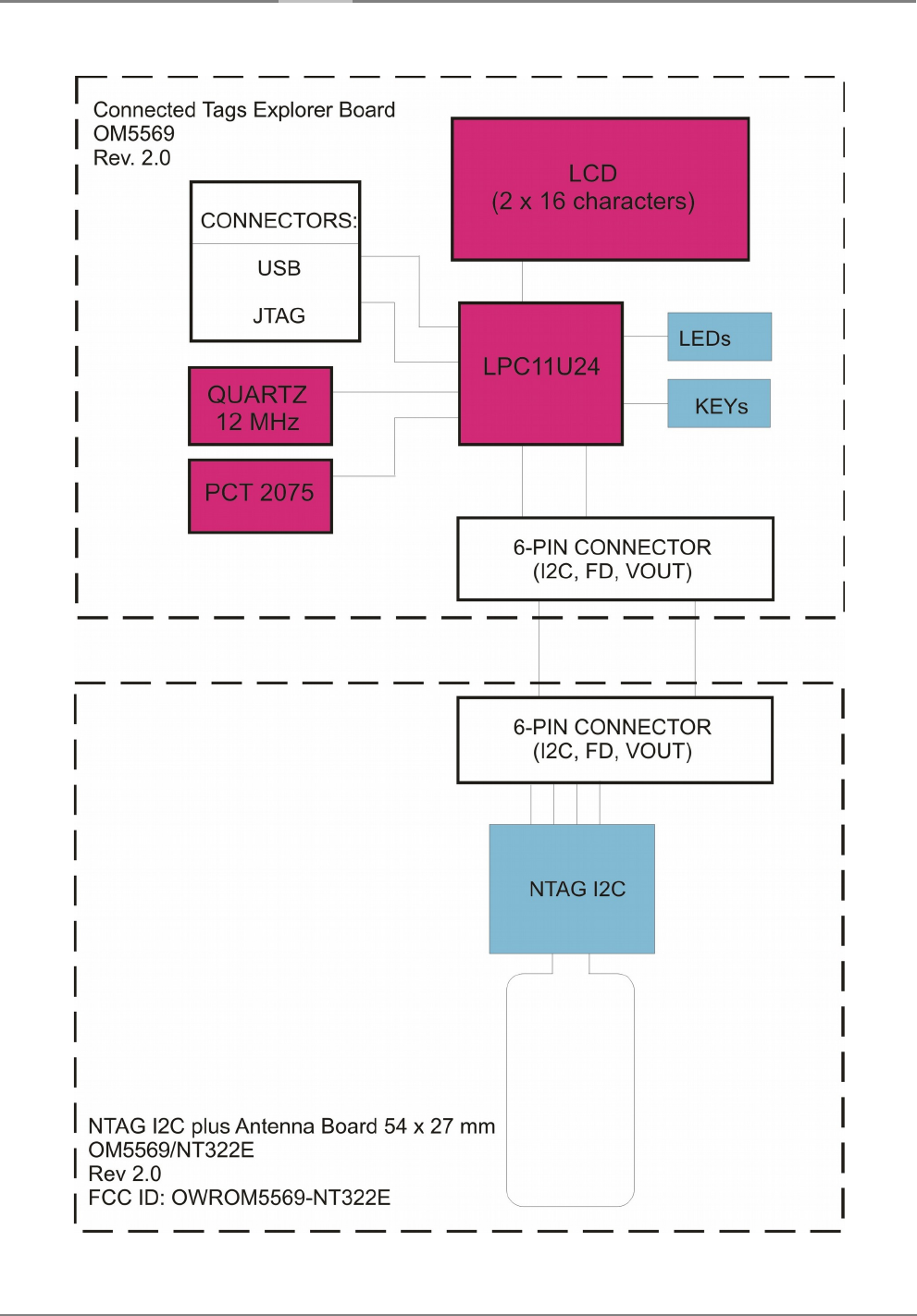
Figure 6: Connected Tags Explorer Board Rev. 2.0 with NTAG I2C plus Antenna Board –
Block diagram.
SRSt Template 1.0 public © NXP B.V. 2015. All rights reserved
Doc ID: DOC-XXXXXX Doc Rev 1.00 Approved — 2015.09.01 7 of 18
BL ID Hardware Manual
Project Name: Integration Manual Project ID: 62743
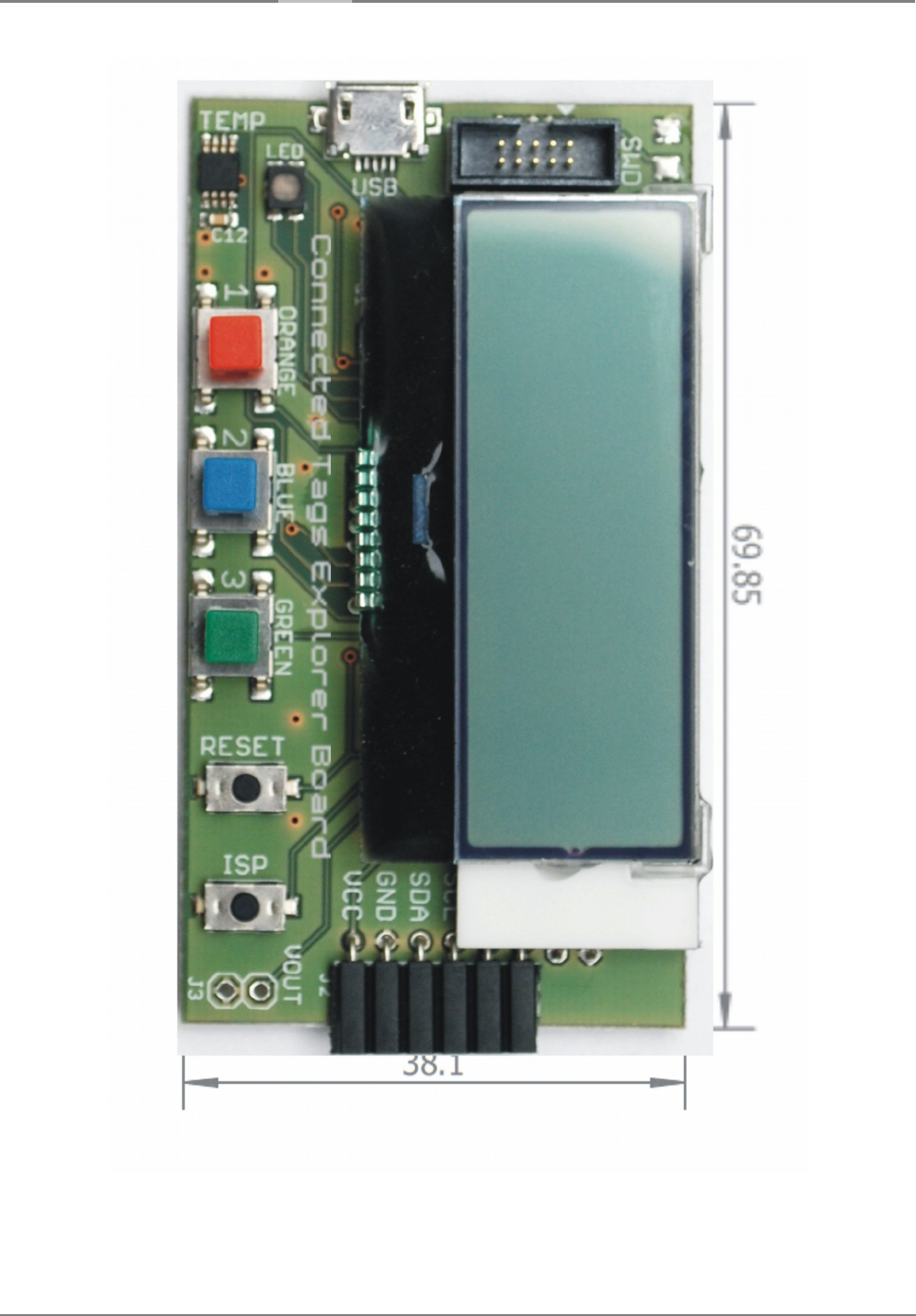
Figure 7: Connected Tags Explorer Board OM5569, Rev. 2.0: dimensions and equipped pcb
with connectors.
SRSt Template 1.0 public © NXP B.V. 2015. All rights reserved
Doc ID: DOC-XXXXXX Doc Rev 1.00 Approved — 2015.09.01 8 of 18
BL ID Hardware Manual
Project Name: Integration Manual Project ID: 62743
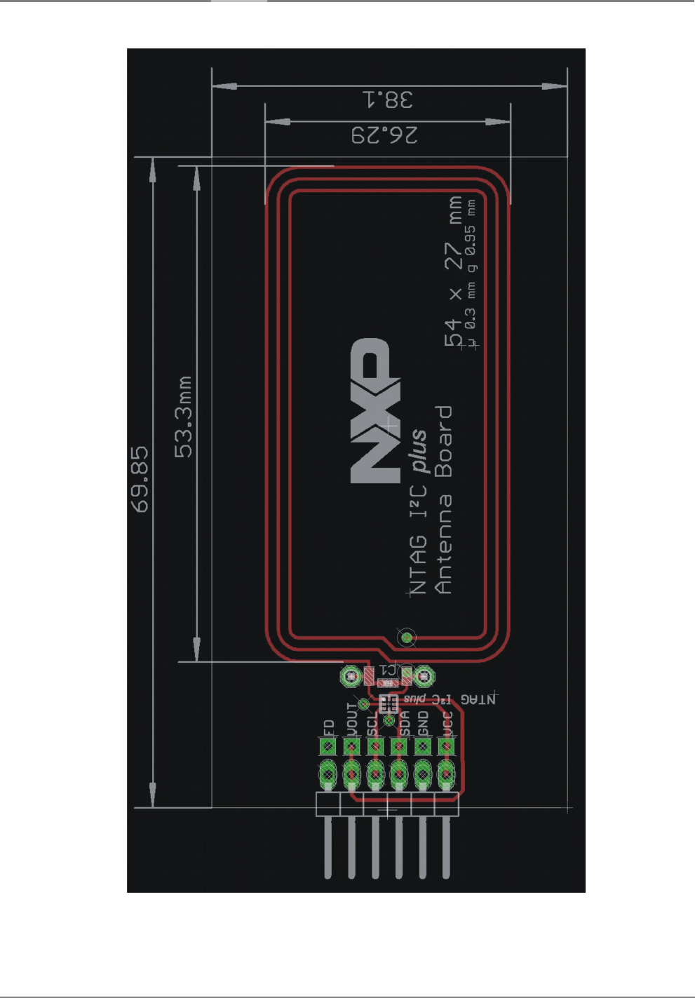
Figure 8: NTAG I2C plus Antenna Board OM5569/NT322E, 54 x 27mm, Rev. 2.0:
dimensions and equipped pcb with connector.
SRSt Template 1.0 public © NXP B.V. 2015. All rights reserved
Doc ID: DOC-XXXXXX Doc Rev 1.00 Approved — 2015.09.01 9 of 18
BL ID Hardware Manual
Project Name: Integration Manual Project ID: 62743
3. NTAG I2C plus Expolorer Kit OM5569/NT322E: SPECIFICATION
3.1. Connected Tags Explorer Board OM5569: Specifications
Table 1: Connected Tags Explorer Board OM5569, Rev. 2.0 – specifications:
Low Power Microcontroller
LPC11U24 (Cortex - M0)
Oscillator
Internal oscillator (in LPC11U24) up to 12 MHz, Quartz 12 MHz
On-board sensor
Temperature Sensor PCT2075
Output/Input
Outputs 3 x LED (orange, green, blue)
Inputs 3 x key
Supported Interfaces (6-pin connector to NTAG I2C Antenna Board)
I2C I2C-bus interface to up to 100 kBd (Standard mode), up to 400 kBs
(Fast mode)
LCD display
2 x 16 character, WLED backlight, I2C serial communication, 3V3
power supply
Supported Interfaces
USB serial interface USB 2.0 interface (also supported Usb 1.1), 12 Mbps (USB 2.0 full
speed), micro usb connector
ISP JTAG interface (10-pin header) for ISP programming with
LPCXpressoBoard
Electrical and Mechanical Specifications
Power Supply Board is powered from NTAG I2C Antenna Board (from NTAG I2C
tag ic); usb power is used only for powering lcd backlight (20 mA)
PCB Dimensions (L x W x
H)
70 mm x 38 mm x 14 mm
Weight approx. 22 g
Operating Temperature 0… + 50 C (without condensing)
Operating Humidity 5 … 95% RH
Certificates CE, FCC
Note:
USB port and JTAG port are used only for writing firmware into LPC11U24 microcontroller
and for debbuging purposes.
SRSt Template 1.0 public © NXP B.V. 2015. All rights reserved
Doc ID: DOC-XXXXXX Doc Rev 1.00 Approved — 2015.09.01 10 of 18
BL ID Hardware Manual
Project Name: Integration Manual Project ID: 62743
3.2. Connected Tags Explorer Board OM5569, Rev. 2.0: Electrical characteristics
Table 2: Connected Tags Explorer Board OM5569, Rev. 2.0 – electrical characteristics:
Operating Range
Symbol Description Conditions Min Typ Max Unit
VCC DC Power Supply (from
NTAG I2C tag ic)
NTAG Active (on NTAG I2C
Antenna Board)
3.0 - 4.6 V
VBUS USB Power Supply (only for
LCD backlight)
NTAG Active (on NTAG I2C
Antenna Board)
4.5 - 5.5 V
Tamb Ambient Temperature / 0 +25 +50 C
Current Consumption
Symbol Description Conditions Min Typ Max Unit
I Supply Current (only
LPC11U24)
Power Down Mode, I2C off - - 0.9 µA
I Supply Current ( LPC11U24,
LCD display, temp. sensor,
LEDs)
Active, I2C on, RF on (on NTAG
I2C Antenna Board)
- - 5 mA
I USB Supply Current (only for
LCD backlight)
Active, I2C on, RF on (on Class 5
Antenna Board)
- 20 - mA
Operating Distance
Symbol Description Conditions Min Typ Max Unit
DST Operating Distance Measured from the center of
the antenna
(depending on connected
antenna and phone NFC
antenna)
- 0 – 30 - mm
Serial Interface Characteristics
Symbol Description Conditions Min Typ Max Unit
I2C Baudrate 6-pin Connector - 100 400 kBd
USB Baudrate Micro B USB Connector - 12 - MBd
SRSt Template 1.0 public © NXP B.V. 2015. All rights reserved
Doc ID: DOC-XXXXXX Doc Rev 1.00 Approved — 2015.09.01 11 of 18
BL ID Hardware Manual
Project Name: Integration Manual Project ID: 62743
3.3. NTAG I2C Antenna Board OM5569/NT322E, Rev 2.0 (54 x 27 mm) –
specifications
Table 3: NTAG I2C plus Antenna Board OM5569/NT322E, Rev 2.0 (54 x 27 mm) –
specifications:
Antenna
PCB type, 54 mm x 27 mm
Contactless operating frequency
13.56 MHz
Card reading/writing distance
Up to 30 mm
Contactless (RF) Interface
NFC forum Type 2 Tag compliant with data transfer 106 Kbps
transmission rate
64 byte SRAM buffer for fast transfer of data between the RF and the
I2C interfaces
Unique 7 byte serial number (cascade level 2 according to ISO/IEC
14443-3)
True anticollision
Supported Interfaces (via 6-pin connector to NATG I2C Main Board)
I2C I2C-bus interface to up to 100 kBd (Standard mode), up to 400 kBs
(Fast mode)
Supported HW Functions (NTAG I2C ic)
FD Field Detect function – wake up signal at the Field Detect pin
EH Energy Harvesting function for power external devices (low power
microcontroller)
Electrical and Mechanical Specifications
Power Supply NTAG I2C tag ic is powered from RF Field (from NFC phone)
PCB Dimensions (L x W x
H)
70 mm x 38 mm x 7 mm
Weight approx. 9 g
Operating Temperature 0 … + 50 C (without condensing)
Operating Humidity 5 … 95% RH
Certificates CE, FCC
SRSt Template 1.0 public © NXP B.V. 2015. All rights reserved
Doc ID: DOC-XXXXXX Doc Rev 1.00 Approved — 2015.09.01 12 of 18

BL ID Hardware Manual
Project Name: Integration Manual Project ID: 62743
4. INSTALLING MANUAL
4.1. Desktop use
NTAG I²C plus Explorer Kit OM5569/NT322E consists from Connected Tags Explorer Board
OM5569 with NTAG I2C plus Antenna Board OM5569/NT322E 54 x 27 mm.
It is intended for development use in development environment such are development
departements in factories, at institutes, etc. It demonstrates the unique properties of the
NTAG I²C tag chip.
External power supply is not required (only for LCD backlight – but it is not necessary for
operating Connected Tags Explorer Board).
Firmware is already written in LPC11U24 microcontroller and no extra programming via
JTAG interface is needed. A NFC mobile phone is needed for demonstration (an application
for mobile phone is avaliable on Android market). User can write his own application and
write it via JTAG interface into microcontroller.
4.2. Power supply
Connected Tags Explorer Board with NTAG I²C plus Anttena Board is powered via RF field
from NFC mobile phone (13,56 MHz). It is no need for external power supply or battery (only
for LCD backlight - but it is not necessary for operating NTAG I²C Explorer Board).
NTAG I²C tag ic on NTAG I²C plus Antenna Board provides up to 2V with 5 mA current
output (typical) on Vout pin. This is enough to power low power microcontroller LPC11U24,
LCD display, temperature sensor and LED.
Note 1:
Power supply from USB port on personal computer has to comply with LPS requirement of
IEC60950-1.
Maximum lenght for USB cable is 3 meter.
SRSt Template 1.0 public © NXP B.V. 2015. All rights reserved
Doc ID: DOC-XXXXXX Doc Rev 1.00 Approved — 2015.09.01 13 of 18

BL ID Hardware Manual
Project Name: Integration Manual Project ID: 62743
5. USER MANUAL
The NTAG I²C plus Explorer Kit is developed to demonstrate the unique properties of the
NTAG I²C tag chip.
The NTAG I²C plus Explorer Kit consists from two boards: Connected Tags Explorer Board
and NTAG I²C plus Antenna board. The Connected Tags Explorer Board contains an NXP
microcontroller (LPC11U24 Cortex-M0), three LEDs (orange, blue and green), three buttons
as well as an temperature sensor (PCT 2075), LCD display. The NTAG I²C plus Antenna
board contains NTAG I2C intergated circuit and pcb wired antenna. Connection between
these two boards is via I2C serial link.
The Android application, called NTAG I2C Demo, can be found and freely downloaded from
the Google Play Store. The Android application is intended to operate on devices running
Android version 4.0 and beyond. The application has been optimized for a correct visioning
of the graphical elements in smartphones featuring different resolutions.
How to test functionality of NTAG I²C tag ic with android application is written in detail in
document: NTAG I2C Explorer Board Programming and Testing.pdf.
CAUTION
The NTAG I²C plus Explorer Kit contains components that can be potentially damaged by
electrostatic discharge. Always store and transport the NTAG I²C plus Explorer Kit in the
supplied ESD bag when not in use. Always handle the NTAG I²C plus Explorer Kit in an ESD
controlled environment.
5.1. Main Functions
-Sending and receiving data to/from NTAG I²C tag ic to NFC Mobile Device via RF
contactless communication (13,56 MHz).
-Supportting contactless RF communication ic according NFC Forum Type 2 tag
compliant protocol.
-Supportting RF data transmission with 106 Kbps transmission rate.
-Communicatin with NFC Mobile device in distance up to 30 mm.
-The data exchange from Explorer Board to NTAG I²C plus Antenna Board (via I2C serial
communication).
-NTAG I²C plus Explorer Kit is powering via RF field from NFC Mobile Device.
SRSt Template 1.0 public © NXP B.V. 2015. All rights reserved
Doc ID: DOC-XXXXXX Doc Rev 1.00 Approved — 2015.09.01 14 of 18

BL ID Hardware Manual
Project Name: Integration Manual Project ID: 62743
5.2. General functions
-Reading/writing to/from NTAG I2C tag ic is possible with NFC mobile phone with android
application.
-Explorer Board with NTAG I2C plus Antenna Board can communicate with NFC mobile
phone in distance up to 30 mm from the center of the NTAG I2C plus Antenna Board to
the center of phone NFC antenna.
-Data transfer from/to NTAG I2C tag ic is possible in RF electromagnetic field (created from
NFC phone). Nonmetal material between phone antenna and NTAG I2C plus Antenna
Board has no influence to reading distance or reading reliability.
-Reading/writing to/from NTAG I2C tag ic is very simple: user approaches his Connected
Tags Explorer Board with NTAG I2C plus Antenna board to NFC phone antenna. The
android application, called NTAG I2
I2C Demo NFC, must be started on mobile phone. User
can turn on/off LEDs on NTAG I2C plus Explorer Kit (with android application) to
demonstrate communication with NTAG I2C tag ic or can press the switches on
Connected Tags Explorer Board (and see pressed switches on android application).
5.3. Instructions for safe work, maintaining and care
•Be careful not to damage the connectors, antenna, PCB, ICs and other connected
parts.
•Because of the specifics of the device and the damage, only quallified staff, authorized
by the producer, are allowed to repair the device. All interventions of the unauthorized
person and mechanical damage means repealing of the guarantee.
SRSt Template 1.0 public © NXP B.V. 2015. All rights reserved
Doc ID: DOC-XXXXXX Doc Rev 1.00 Approved — 2015.09.01 15 of 18

BL ID Hardware Manual
Project Name: Integration Manual Project ID: 62743
6. ELECTROMAGNETIC COMPATIBILITY
NTAG I²C plus Explorer Kit fulfils the following requirements of electromagnetic compatibility:
FCC, Part 15.
6.5.1. FCC Compliance Statement
NOTE:
This equipment has been tested and found to comply with the limits for a Class B digital
device, pursuant to Part 15 of the FCC Rules. These limits are designed to provide
reasonable protection against harmful interference when the equipment is operated in a
residential environment. This equipment generates, uses, and can radiate radio frequency
energy and, if not installed and used in accordance with the instruction manual, may cause
harmful interference to radio communications. However, there is no guarantee that
interference will not occur in a particular installation. If this equipment does cause harmful
interference to radio or television reception, which can be determined by turning the
equipment off and on, the user is encouraged to try to correct the interference by one or
more of the following measures:
- Reorient or relocate the receiving antenna.
- Increase the separation between the equipment and receiver.
- Connect the equipment into an outlet on a circuit different from that to which the receiver
is connected.
- Consult the dealer or an experienced radio/TV technician for help.
Caution!
The Federal Communications Commission warns the users that changes or modifications to
the unit not expressly approved by the party responsible for compliance could void the user’s
authority to operate the equipment.
SRSt Template 1.0 public © NXP B.V. 2015. All rights reserved
Doc ID: DOC-XXXXXX Doc Rev 1.00 Approved — 2015.09.01 16 of 18

BL ID Hardware Manual
Project Name: Integration Manual Project ID: 62743
6.5.2. COMPLIANCE INFORMATION according to 47CFR 2.1033
We, declare that the product
NTAG I²C plus Explorer Kit OM5569/NT322E
FCC 12.225, FCC ID: OWROM5569-NT322E
is in conformity with Part 15 of the FCC Rules.
Operation of this product is subject to the following conditions:
(1) this device may not cause harmful interference
(2) this device must accept any interference received, including interference that may
cause undesired operation.
Note:
Any changes or modifications not expressly approved by the party responsible for
compliance could void the user's authority to operate the equipment.
NTAG I2C plus Explorer Kit OM5569/NT322E consists from Connected Tags Explorer Board
and NTAG I2C plus Antenna Board (54 x 27 mm). FCC certified is Connected Tags Explorer
Board OM5569 with NTAG I2C plus Antenna Board OM5569/NT322E 54 x 27 mm.
FCC ID number is written only on NTAG I2C plus Antenna Board OM5569/NT322E 54 x 27
mm.
SRSt Template 1.0 public © NXP B.V. 2015. All rights reserved
Doc ID: DOC-XXXXXX Doc Rev 1.00 Approved — 2015.09.01 17 of 18

BL ID Hardware Manual
Project Name: Integration Manual Project ID: 62743
WARRANTY, LIMITATIONS OF LIABILITY
WARRANTY POLICY
Manufacturer warrants that any product (“Product“) sold by Manufacturer to an end user
(“User”) shall be free of defects in material and workmanship for a period a one year (or other
period if specified) from date of sale by Manufacturer.
If any Product, Product's part fail to conform or is defective then Manufacturer, at its option,
will repair or replace it at the premises of the User (On-Site).
To obtain warranty service, you must send the Product in either its original packaging or
packaging offering an equal degree of protection directly to Manufacturer. Please contact
Manufacturer for warranty replacement fee information.
LIMITATIONS AND EXCLUSIONS
This warranty does not cover customer instruction, installation, set up adjustments or signal
reception problems (RFID readers).
This warranty does not cover cosmetic damage or damage due to acts of God, accident,
misuse, abuse, negligence, commercial use, or modification of, or to any part of the Product,
including the antenna. This warranty does not cover damage due to improper operation or
maintenance, connection to improper voltage supply, or attempted repair by anyone other
than a facility authorized by Manufacturer to service the Product.
Proof of purchase in the form of a bill of sale or receipted invoice which is evidence that the
unit is within the Warranty period must be presented to obtain warranty service.
This warranty is invalid if the factory applied serial number has been altered or removed from
the Product.
THIS WARRANTY REPRESENTS THE ENTIRE AGREEMENT BETWEEN
MANUFACTURER AND USER WITH RESPECT TO THE SUBJECT MATTER HEREIN AND
SUPERSEDES ALL PRIOR OR CONTEMPORANEOUS ORAL OR WRITTEN
COMMUNICATIONS, REPRESENTATIONS, UNDERSTANDINGS OR AGREEMENTS
RELATING TO THIS SUBJECT.
End User: _________________________________________________________
Model Number: _____ NATG I 2
C plus Explorer_Kit, OM5569/NT322E_______________
Serial Number: _____________________________________________________
Startup Date: __________________ Waranty End Date: _________________
SRSt Template 1.0 public © NXP B.V. 2015. All rights reserved
Doc ID: DOC-XXXXXX Doc Rev 1.00 Approved — 2015.09.01 18 of 18