NXP Austria PNEV5180B PN8180 Customer Evaluation Board User Manual Integration Manual EXPLORE NFC
NXP Austria GmbH PN8180 Customer Evaluation Board Integration Manual EXPLORE NFC
UserManual.wiki
>
NXP Austria
>
PNEV5180B User Manual
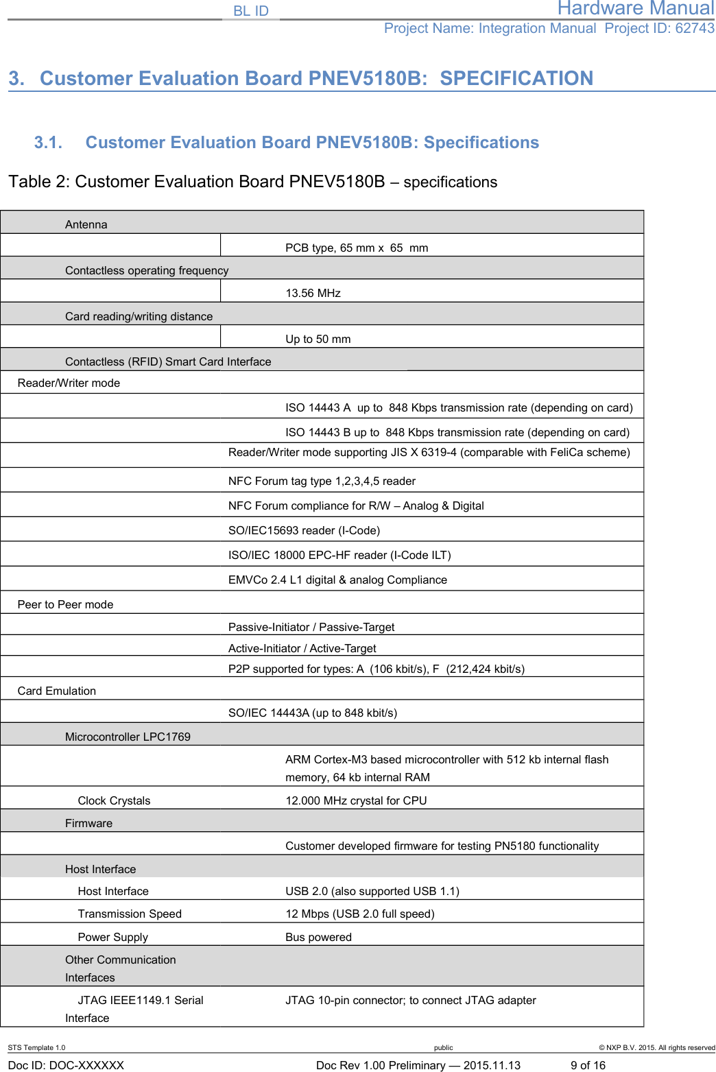
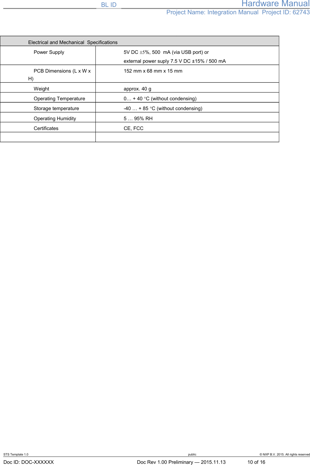
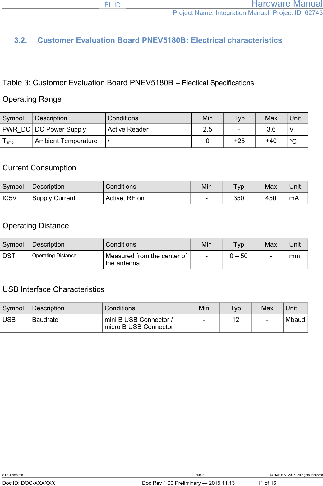
Hardware Manual
Navigation menu
Upload a User Manual
Namespaces
Wiki Guide
HTML
PDF
Info
Views
User Manual
Discussion / Help
Navigation