NXP Austria PNEV7462B PN7462AU Customer Demo Board User Manual Integration Manual EXPLORE NFC
NXP Austria GmbH PN7462AU Customer Demo Board Integration Manual EXPLORE NFC
Manual
Document information
Info Content
Author Pavel Slamnik
Author Role Design Engineer
Keywords PN7462AU Customer Demo Board, PNEV7462B, RFID, NFC,
Integration Manual: PN7462AU Customer
Demo Board, PNEV7462B
Doc Rev 1.00 Approved — 2016 BL ID

BL ID Integration Manual
Project Name: Integration Manual Project ID: 62766
Revision History
Revision Date Description Author
1.0 2016.07.15 First Version Pavel Slamnik
SRS Template_vs 1.0 public © NXP B.V. 2016. All rights reserved
Doc ID: DOC-XXXXXX Doc Rev 1.00 Approved — 2016.07.15 2 of 16
Copyright: @2009, NXP Semiconductors
The information contained herein is the exclusive and confidential property of NXP Semiconductors and, except as
otherwise indicated, shall not be disclosed or reproduced in whole or in part.

BL ID Integration Manual
Project Name: Integration Manual Project ID: 62766
Contents
SRSt Template 1.0 public © NXP B.V. 2016. All rights reserved
Doc ID: DOC-XXXXXX Doc Rev 1.00 Approved — 2016.07.15 3 of 16

BL ID Integration Manual
Project Name: Integration Manual Project ID: 62766
STS Template 1.0 public © NXP B.V. 2016. All rights reserved
Doc ID: DOC-XXXXXX Doc Rev 1.00 Preliminary — 2016.07.15 4 of 16
BL ID Integration Manual
Project Name: Integration Manual Project ID: 62766
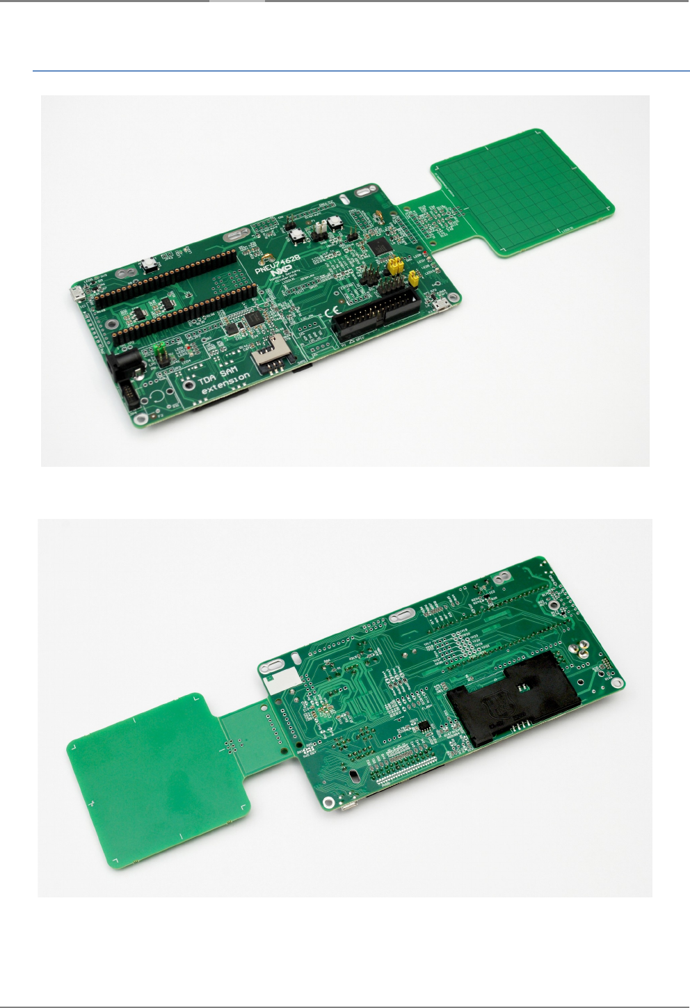
1. PN7462AU Customer Demo Board PNEV7462B: Photo
Figure 1: PN7462AU Customer Demo Board PNEV7462B – side view.
Figure 2: PN7462AU Customer Demo Board PNEV7462B – top view.
STS Template 1.0 public © NXP B.V. 2016. All rights reserved
Doc ID: DOC-XXXXXX Doc Rev 1.00 Preliminary — 2016.07.15 5 of 16

BL ID Integration Manual
Project Name: Integration Manual Project ID: 62766
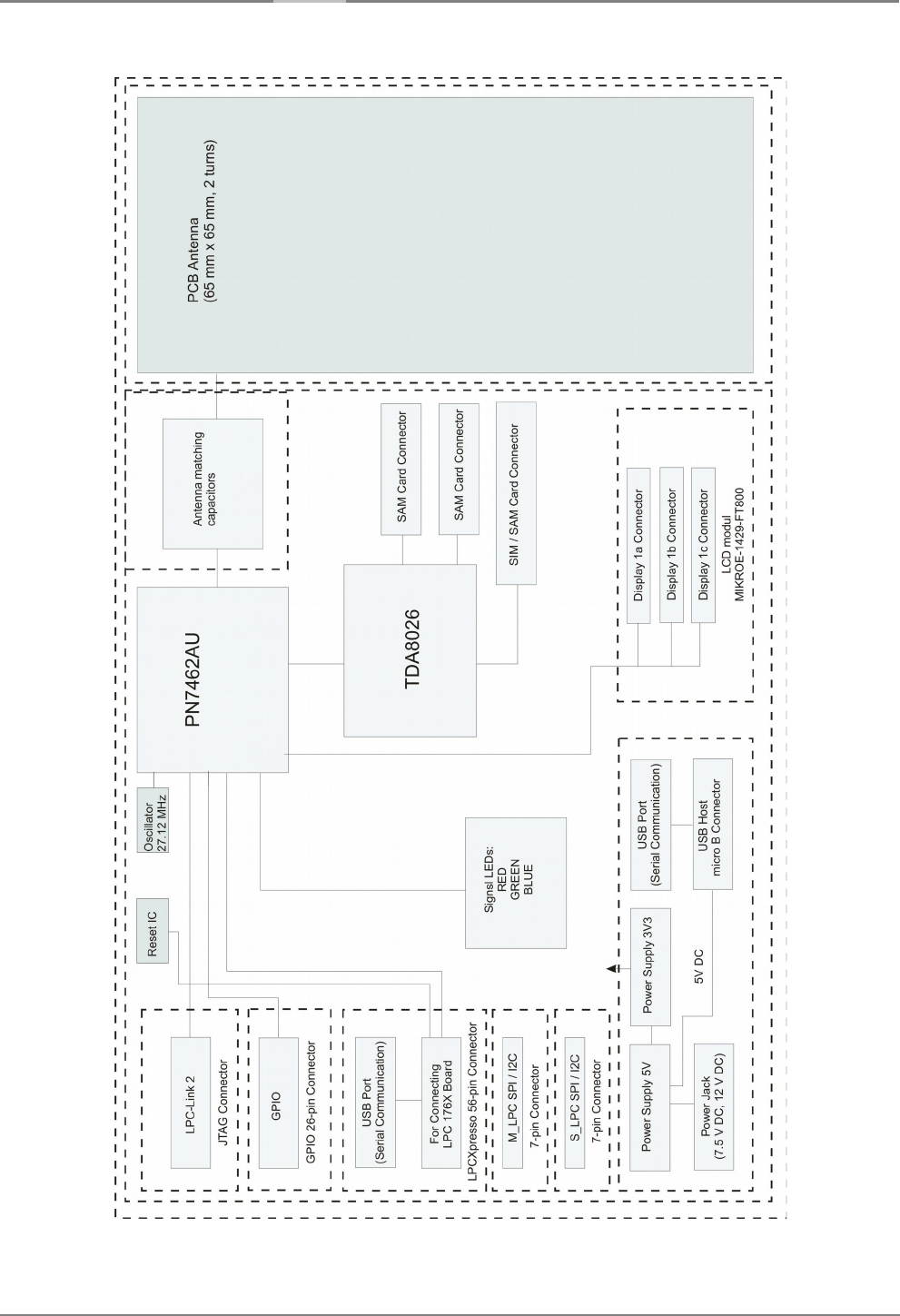
2. PN7462AU Customer Demo Board PNEV7462B: Description
1. Operational desription
PN7462AU Customer Demo Board, PNEV7462B, is first enaluation board which represents one single
integrated circuit controller solution for state-of-the-art RF interface (ISO/IEC 14443, ISO/IEC 15693, ISO/IEC
18000-3m3, Full NFC support) and contact interface (ISO/IEC 7816).
It includes Cortex-M0 core microcontroller and it can be loaded with fully-custom applications. Optimized RF
antenna operation and low-power modes enable best-in-class performance. The onboard two USB connectors
permits direct connection and communication with personal computer. LPC-Link2 debug adapter is added on
the board. Also LPCExpresso connector to add a LPCExpresso board is present too. For smart card evaluation
purposes are added two different connectors.
The heart of this Customer Demo Board is PN7462AU integrated circuit which includes at the same silicon:
· 20 MHz Cortex-M0 core microcontroller with 160 kB Flash memory for application code
· State-of-the-art RF interface (ISO/IEC 14443, ISO/IEC 15693, ISO/IEC 18000-3m3, Full NFC support)
· contact interface (ISO/IEC 7816)
· different communication ports / controllers.
· EMVCo and NFC forum compliances
NFC part of PN7462AU ic is a highly integrated high power output NFC frontend for contactless communication
at 13.56 MHz. This frontend part of IC utilizes an outstanding modulation and demodulation concept completely
integrated for different kinds of contactless communication methods and protocols at 13.56 MHz. Matching
capacitors are needed for proper connection between pcb antena and NFC part of IC PN7462AU power output.
Optimized RF antenna operation and low-power modes enable best-in-class performance.
Microcontroller part of PN7462AU ic consists from Cortex-M0 microcontroller with 160 kB flash memory, 12 kB
RAM and 4 kB EEPROM memory. Different communication interfaces (serial and GPIO ports) permits USB
communication to personal computer, I2C and SPI ports to LPCXpresso board, JTAG connection to LPC-LINK2
board, SPI and I2C serial communication with external boards (option). JTAG connector is needed to connect
computer to write application into PN7462AU Cortex-M0 microcontrollers flash memory and EEPROM. As an
option also is provided connection to external LCD modul.
ISO/IEC 7816 interface part of PN7462AU ic is connected via TDA8026 (multiple smart card slot interface ic) to
three SIM /SAM card connectors.
Some status LEDs are added for indicating Customer demo Board PNEV7462B states (readin or writing cards,
mode status, erros etc.). Some test points are added to check states on pins.
The onboard two USB connectors permits direct connection and communication with personal computer. LPC-
Link2 debug adapter is added on the board. Also LPCExpresso connector to add a LPCExpresso board is
present too. LPC-Link2 debug adapter is added on the board. Also LPCExpresso connector to add a
LPCExpresso board is present too. For smart card evaluation purposes are added two different connectors.
Power supply for PNEV7462B board is via one of two usb ports or via external power supply (7.0 … 13.5 V
DC / 1000 mA).
Disclaimer :
This module is intended only for development and evaluation purposes, and cannot be used in a finished
product.
STS Template 1.0 public © NXP B.V. 2016. All rights reserved
Doc ID: DOC-XXXXXX Doc Rev 1.00 Preliminary — 2016.07.15 6 of 16
BL ID Integration Manual
Project Name: Integration Manual Project ID: 62766
Figure 3: PN7462AU Customer demo Board, PNEV7462B - Block diagram.
STS Template 1.0 public © NXP B.V. 2016. All rights reserved
Doc ID: DOC-XXXXXX Doc Rev 1.00 Preliminary — 2016.07.15 7 of 16
BL ID Integration Manual
Project Name: Integration Manual Project ID: 62766
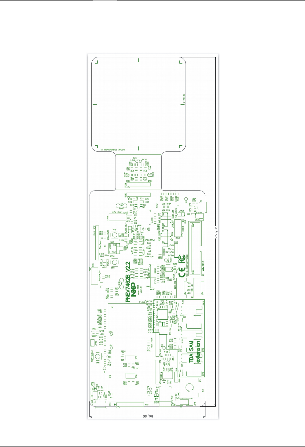
Figure 4: PN7462AU Customer demo Board, PNEV7462B: dimensions, pcb with elements.
STS Template 1.0 public © NXP B.V. 2016. All rights reserved
Doc ID: DOC-XXXXXX Doc Rev 1.00 Preliminary — 2016.07.15 8 of 16
BL ID Integration Manual
Project Name: Integration Manual Project ID: 62766
3. PN7462AU Customer Demo Board, PNEV7462B: SPECIFICATION
3.1. PN7462AU Customer Demo Board, PNEV7462B: Specifications
Table 2: PN7462AU Customer demo Board, PNEV7462B – specifications
Antenna
PCB type, 65 mm x 65 mm
Contactless operating frequency
13.56 MHz
Card reading/writing distance
Up to 50 mm
Contactless (RFID) Smart Card Interface (inside PN7462AU ic)
Reader/Writer mode
ISO 14443 A up to 848 Kbps transmission rate (depending on card)
ISO 14443 B up to 848 Kbps transmission rate (depending on card)
Reader/Writer mode supporting JIS X 6319-4 (comparable with FeliCa scheme)
NFC Forum tag type 1,2,3,4,A and 4B
NFC IP1 and NFC IP2 support
SO/IEC15693 reader (I-Code)
ISO/IEC 153, ICODE, ISO/IEC18000-3
EMVCo 4.3 Compliance
Peer to Peer mode
Passive-Initiator / Passive-Target
Active-Initiator / Active-Target
P2P supported for types: A (106 kbit/s), F (212,424 kbit/s)
Card Emulation
SO/IEC 14443A (up to 848 kbit/s)
Contact Interface (inside
PN7462AU ic)
Class A, B and C cards support (1.8 V, 3 V, 5 V)
ISO/IEC 7816 compliance
Synchronous card support
Clock generation up to 13.56 MHz
Possibility to extend the number of contact interface thanks to the addition of slot
extenders like TDA8026
Automatic activation and deactivation sequence: initiated by software or by
hardware
Microcontroller (inside
PN7462AU ic)
ARM Cortex-M0 based microcontroller with 160 kB internal flash
memory, 12 kB internal RAM, 4 kB internal EEPROM
Clock Crystals 27.12 MHz crystal for PN6742AU
STS Template 1.0 public © NXP B.V. 2016. All rights reserved
Doc ID: DOC-XXXXXX Doc Rev 1.00 Preliminary — 2016.07.15 9 of 16
BL ID Integration Manual
Project Name: Integration Manual Project ID: 62766
Firmware
Customer developed firmware for testing PN6742AU functionality
Host Interface
USB 2.0 12 Mbps (USB 2.0 full speed), bus powered,
SPI Half duplex and full duplex, up to 7 Mbit/s
I2C Supporting fast plus (extended, up to 1 Mbds), multiple address
support
Master Interface
SPI Half duplex, from 1 Mbit/s to 6.78 Mbit/s
I2C Supporting fast mode and clock streching
Power Supply Bus powered
Power Supply 5V DC 5%, 500 mA (via USB port) or
external power suply 7.0 V … 13.5 V DC / 1000 mA
PCB Dimensions (L x W x
H)
259 mm x 86 mm x 12 mm
Weight approx. 88 g
Operating Temperature 0… + 40 C (without condensing)
Storage temperature -40 … + 85 C (without condensing)
Operating Humidity 5 … 95% RH
Certificates CE, FCC
STS Template 1.0 public © NXP B.V. 2016. All rights reserved
Doc ID: DOC-XXXXXX Doc Rev 1.00 Preliminary — 2016.07.15 10 of 16
BL ID Integration Manual
Project Name: Integration Manual Project ID: 62766
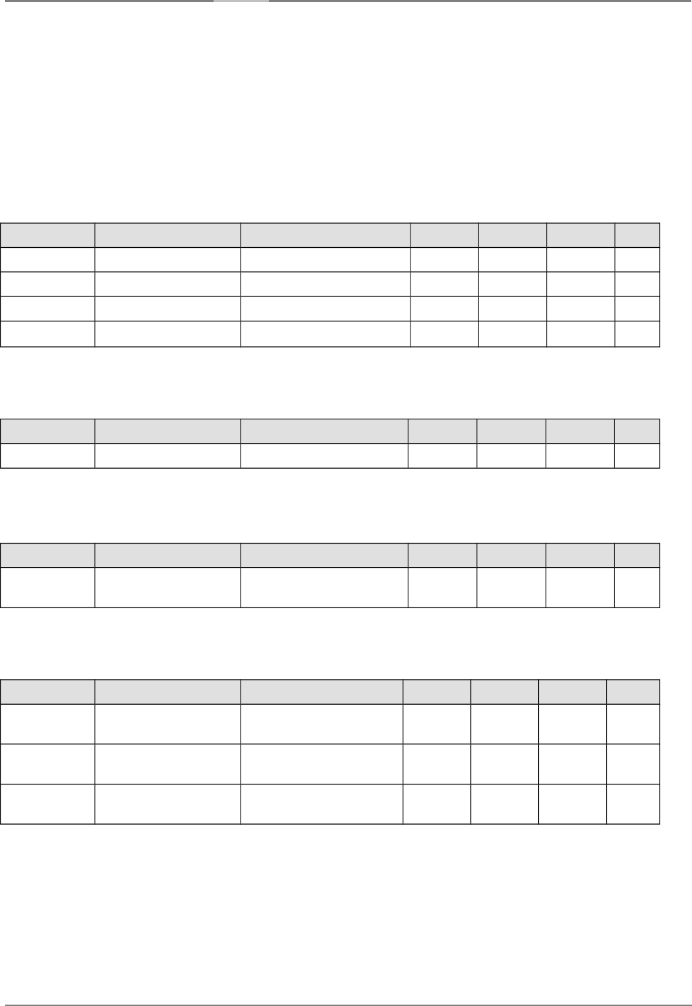
3.2. PN7462AU Customer demo Board, PNEV7462B: Electrical characteristics
Table 3: PN7462AU Customer Demo Board, PNEV7462B – Electical Specifications
Operating Range
Symbol Description Conditions Min Typ Max Unit
7_13.5V_DC AC/DC Power Supply Active Reader 7.0 12.0 13.5 V
VUSB_PN DC Power Supply Active Reader 4.75 5.0 5.25 V
VBUS_LPC DC Power Supply Active Reader 4.75 5.0 5.25 V
Tamb Ambient Temperature / 0 +25 +40 C
Current Consumption
Symbol Description Conditions Min Typ Max Unit
IC5V Supply Current Active, RF on - 300 450 mA
Operating Distance
Symbol Description Conditions Min Typ Max Unit
DST Operating Distance Measured from the
center of the antenna
- 0 – 50 - mm
USB Interface Characteristics
Symbol Description Conditions Min Typ Max Unit
USB Baudrate mini B USB Connector /
micro B USB Connector
- 12 - Mbaud
SPI Baudrate via 52-pin LPCXpresso
connector
- - 7 Mbit/s
I2C Baudrate via 52-pin LPCXpresso
connector
- - 1 Mbit/s
STS Template 1.0 public © NXP B.V. 2016. All rights reserved
Doc ID: DOC-XXXXXX Doc Rev 1.00 Preliminary — 2016.07.15 11 of 16

BL ID Integration Manual
Project Name: Integration Manual Project ID: 62766
4. INSTALLING MANUAL
4.1. Desktop use
PN7462AU Customer Demo Board, PNEV7462B, is intended for development use in
development environment such are development departements in factories, at institutes.
PNEV7462B board is powered via USB serial connection from personal computer or via
external power supply.
Usual climate conditions in development environment (room temperature and humidity) are
deep inside PN7462AU Customer Demo Board specified climate conditions.
4.2. Power supply
PN7462AU Customer Demo Board has no power supply mounted on pcb. There are three
possibilties to connect external power supply:
- powering via one of two USB ports (micro B connector) from personal computer or
- via external power supply 7.0 V … 13.5 V DC / 1000 mA.
Which option is used is set with jumper JP41 (figure cc).
The micro B USB connector is used for connection to the PC usb port – for power supply
and USB serial communication. USB A male to micro B USB (5 pin) cable is used for
connection between PN7462AU Customer Demo Board (PNEV7462B) and personal
computer.
External power supply 7.0 … 13.5 V DC / 1000 mA is connected to power jack P4 to supply
PN7462AU Customer Demo Board. On board IC NCP1117LP is used to stabilize voltage to
5 V.
Note 1:
Power supply from USB port on personal computer has to comply with LPS requirement of
IEC60950-1.
Maximum lenght for USB cable is 3 meter.
Note 2:
External power supply 7.0 V … 13.5 V DC / 1000 mA has to comply with LPS requirement of
IEC60950-1.
Maximum lenght for power cable is 3 meter.
STS Template 1.0 public © NXP B.V. 2016. All rights reserved
Doc ID: DOC-XXXXXX Doc Rev 1.00 Preliminary — 2016.07.15 12 of 16

BL ID Integration Manual
Project Name: Integration Manual Project ID: 62766
5. USER MANUAL
PN7462AU Customer Demo Board, PNEV7462B, is an example of implementation of
ISO/IEC 14443A and ISO/IEC 14443B reader/writer, NFC reader/writer, Card Emulation
Device and Contact Card Reader on the same printed board. Middle size antenna,
implemented on the same pcb (reader and antenna can be broken into separate parts),
permits reading/writing on distance up to 50 mm (RFID card or other NFC device). The
onboard USB connector permits direct connection and communication with personal
computer.
PN7462AU Customer Demo Board, PNEV7462B, is inteded to send and receive data
according to the ISO 14443A and ISO 14443B protocol. Data transfer from reader to/from
contactless cards operates at frequency 13.56 MHz. Data transfer between PN7462AU
reader IC and personal computer is via USB port. Data transfer between PN7462AU reader
IC and LPTXpresso board is via SPI or I2C serial communication.
The firmware for testing and development purposes is written into PN7462AU (into flash
memory). But user can develop his own firmware and write it via JTAG port into PN7462AU
memory.
Power supply is via usb port or via external power supply ( 7.0 V … 13.5 V DC / 1000 mA).
How to installing user developed firmware is written in detail in Quick Start Guide (and ARM
Board User Manual).
5.1. General user instructions
-Reading/writing is possible with MIFARE contactless cards, FeliCa cards or with NFC
device.
-PNEV7462B board can detect contactless card or NFC device up to 50 mm from the
center reader's antenna.
-PNEV7462B board can emulate contactless (NFC) card.
-Contactless card identification is possible in electromagnetic field (created from
contactless reader). Nonmetal material between antenna and RFID contactless card
have no influence to reading distance or reading reliability.
-Reading/writing to/from card is very simple: user approaches his contactless card to
reader's antena. PNEV7462B board detects card and confirm reading via serial (USB)
communication to personal computer (depend from customer firmware). Successfully
reading/writing can be signalised with status led diode on PNEV7462B board.
STS Template 1.0 public © NXP B.V. 2016. All rights reserved
Doc ID: DOC-XXXXXX Doc Rev 1.00 Preliminary — 2016.07.15 13 of 16

BL ID Integration Manual
Project Name: Integration Manual Project ID: 62766
5.2. Instructions for safe work, maintaining and care
•Be careful not to damage the connectors, antenna, PCB, ICs and other connected
parts.
•Because of the specifics of the device and the damage, only quallified staff, authorized
by the producer, are allowed to repair the device. All interventions of the unauthorized
person and mechanical damage means repealing of the guarantee.
STS Template 1.0 public © NXP B.V. 2016. All rights reserved
Doc ID: DOC-XXXXXX Doc Rev 1.00 Preliminary — 2016.07.15 14 of 16

BL ID Integration Manual
Project Name: Integration Manual Project ID: 62766
6. ELECTROMAGNETIC COMPATIBILITY
PN7462AU Customer Demo Board, PNEV7462B, fulfils the following requirements of
electromagnetic compatibility:
FCC, Part 15 and CE.
6.1 FCC Compliance Statement
NOTE:
This equipment has been tested and found to comply with the limits for a Class B digital
device, pursuant to Part 15 of the FCC Rules. These limits are designed to provide
reasonable protection against harmful interference when the equipment is operated in a
residential environment. This equipment generates, uses, and can radiate radio frequency
energy and, if not installed and used in accordance with the instruction manual, may cause
harmful interference to radio communications. However, there is no guarantee that
interference will not occur in a particular installation. If this equipment does cause harmful
interference to radio or television reception, which can be determined by turning the
equipment off and on, the user is encouraged to try to correct the interference by one or
more of the following measures:
- Reorient or relocate the receiving antenna.
- Increase the separation between the equipment and receiver.
- Connect the equipment into an outlet on a circuit different from that to which the receiver
is connected.
- Consult the dealer or an experienced radio/TV technician for help.
FCC Compliance for Limited Modular Approval (§15.212(b))
As note, the module is intended for PROFESSIONAL AND DEVELOPMENT USE ONLY and
cannot be used in final products. The module is tested to comply with relevant part 15 rules
without shielding and in the same configuration as it is intended to be used by developer.
PNEV7462B board has passed spurious emissions test without shielding and is certified as
limited modular transmitter. Under FCC part 15.212(b), shielding is not required.
Concerning §2.803 the PNEV7462B board will be not offered for sale to other parties or to
end users located in a residential environment.
Caution!
The Federal Communications Commission warns the users that changes or modifications to
the unit not expressly approved by the party responsible for compliance could void the user’s
authority to operate the equipment.
STS Template 1.0 public © NXP B.V. 2016. All rights reserved
Doc ID: DOC-XXXXXX Doc Rev 1.00 Preliminary — 2016.07.15 15 of 16

BL ID Integration Manual
Project Name: Integration Manual Project ID: 62766
6.2 COMPLIANCE INFORMATION according to 47CFR 2.1033
We, declare that the product
PN7462AU Customer Demo Board, PNEV7462B
FCC 12.225, Limited Modular Approval, FCC ID: OWRPNEV7462B
is in conformity with Part 15 of the FCC Rules.
Operation of this product is subject to the following conditions:
(1) this device may not cause harmful interference
(2) this device must accept any interference received, including interference that may
cause undesired operation.
Note:
Any changes or modifications not expressly approved by the party responsible for
compliance could void the user's authority to operate the equipment.
STS Template 1.0 public © NXP B.V. 2016. All rights reserved
Doc ID: DOC-XXXXXX Doc Rev 1.00 Preliminary — 2016.07.15 16 of 16