NXP Laboratories UK JN5139M4 JN5139-000-M04 Wireless Microcontroller User Manual JN DS JN513x
NXP Laboratories UK Ltd JN5139-000-M04 Wireless Microcontroller JN DS JN513x
UserManual.wiki
>
NXP Laboratories UK
>
JN5139M4 User Manual
>
Manual
Contents
1.
User Manual
2.
Manual
3.
Antenna Info 1
4.
Antenna Info 2
5.
Antenna Info 3
6.
Antenna Info 4
7.
Antenna Info 5
8.
Antenna Info 6
9.
Antenna Info 7
10.
Antenna Info 8
11.
Antenna Info 9
12.
manual
13.
Antenna Info 10
14.
Antenna Info 11
Manual
Navigation menu
Upload a User Manual
Namespaces
Wiki Guide
HTML
PDF
Info
Views
User Manual
Discussion / Help
Navigation
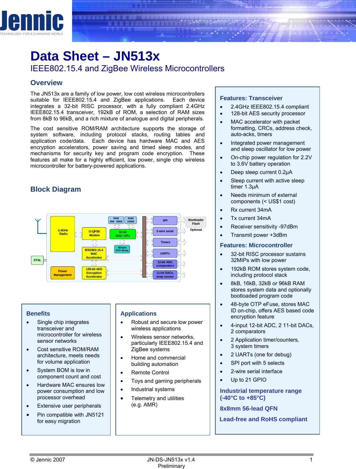
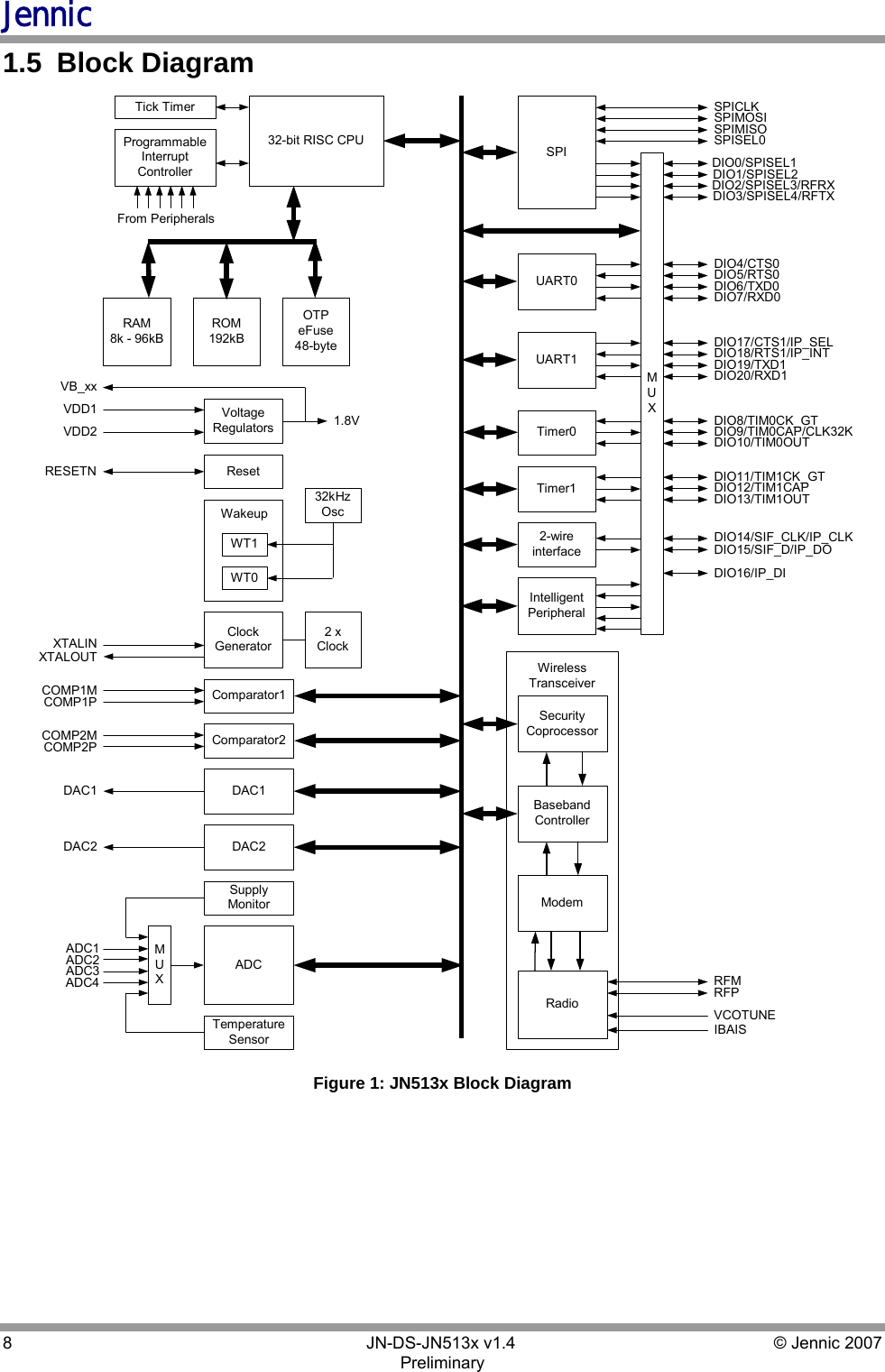
![Jennic 6 JN-DS-JN513x v1.4 © Jennic 2007 Preliminary 1 Introduction The JN513x is an IEEE802.15.4 wireless microcontroller that provides a fully integrated solution for applications using the IEEE802.15.4 standard in the 2.4 - 2.5GHz ISM frequency band [1], including ZigBee. It includes all of the functionality required to meet the IEEE802.15.4 specification and has additional processor capability to run a wide range of applications including but not limited to Remote Control, Home and Building Automation, Toys and Gaming. The device includes a Wireless Transceiver, RISC CPU, on-chip memory and an extensive range of peripherals. 1.1 Wireless Microcontroller Applications that transfer data wirelessly tend to be more complex than wired ones. Wireless protocols make stringent demands on frequencies, data formats, timing of data transfers, security and other issues. Application development must consider the requirements of the wireless network in addition to the product functionality and user interfaces. To minimise this complexity, Jennic provides a series of software libraries that control the transceiver and peripherals of the JN513x. These libraries, with functions called by an Application Programming Interface (API) remove the need for the developer to understand wireless protocols and greatly simplify the programming complexities of power modes, interrupts and hardware functionality. In addition, the JN513x is expected to be programmed in the C high-level language and debugged using the JN5 series software developer kit. In view of the above, the register details of the JN513x are not provided in the datasheet and access to all peripherals is gained using API calls to the peripheral library. Extensive reference to such calls is made throughout the datasheet and the convention used is to format the function call in the courier font e.g. vAHI_Init(). Full details of these function calls can be found in the JN-RM-2001 Integrated Peripherals API [2]. An IEEE802.15.4 compliant wireless network can be developed using the IEEE802.15.4 MAC library described in JN-RM-2002 802.15.4 Stack [3]. Applications over simple (point-point, star or tree) wireless networks can use this library directly or more complex wireless mesh networks such as ZigBee or IPv6 can be built on top of the IEEE802.15.4 library. 1.2 Wireless Transceiver The Wireless Transceiver is highly integrated and, together with the IEEE802.15.4 MAC library requires little knowledge of RF or wireless design. The Wireless Transceiver comprises a low-IF 2.45GHz radio, an O-QPSK modem, a baseband controller and a security coprocessor. The radio has a 200Ω resistive differential antenna port that includes all the required matching components on-chip, allowing a differential antenna to be connected directly to the port, minimising the system BOM costs. Connection to a single ported antenna can be achieved using a 200/50Ω 2.45GHz balun. In addition, the radio also provides an output to control transmit-receive switching of external devices such as power amplifiers allowing applications that require increased transmit power to be realised very easily. The Security coprocessor provides hardware-based 128-bit AES-CCM, CBC(1), CTR and CCM* processing as specified by the 802.15.4b standard. It does this in-band on packets during transmission and reception, requiring minimal intervention from the CPU. It is also available for off-line use under software control for encrypting and decrypting packets generated by software layers such as Zigbee and user applications. This means that these algorithms can be off-loaded by the CPU, increasing the processor bandwidth available for user applications. The transceiver elements (radio, modem and baseband) work together to provide 802.15.4 Medium Access Control under the control of a protocol stack supplied with the device as a software library. Applications incorporating IEEE802.15.4 functionality can be rapidly developed by combining user-developed application software with this library. The facilities provided by this library to applications together with examples of their use are described in more detail in [3]. (1) AES-CBC processing is only available off-line for use under software control. 1.3 RISC CPU and Memory A 32-bit RISC CPU allows software to be run on-chip, its processing power being shared between the IEEE802.15.4 MAC protocol, other higher layer protocols and the user application. The JN513x has a unified memory architecture, code memory, data memory, peripheral devices and I/O ports are organized within the same linear address space. The device contains 192kBytes of ROM, a choice of 8k, 16k, 32k or 96kBytes of RAM and a 48-byte OTP eFuse memory.](https://usermanual.wiki/NXP-Laboratories-UK/JN5139M4.Manual/User-Guide-933298-Page-6.png)
![Jennic © Jennic 2007 JN-DS-JN513x v1.4 7 Preliminary 1.4 Peripherals The following peripherals are available on-chip: • Master SPI port with five select outputs • Two UARTs • Two programmable Timer/Counters with capture/compare facility • Two programmable Sleep Timers and a Tick Timer • Two-wire serial interface (compatible with SMbus and I2C) • Slave SPI port (shared with digital I/O) • Twenty-one digital I/O lines (multiplexed with UARTs, timers and SPI selects) • Four-channel, 12-bit, 100ksps Analogue-to-Digital converter • Two 11-bit Digital-to-Analogue converters • Two programmable analogue comparators • Internal temperature sensor and battery monitor User applications access the peripherals using the Hardware Peripheral Library with a simple API. This allows applications to use a tested and easily understood view of the peripherals allowing rapid system development. The JN-RM-2001 Integrated Peripherals API [2] describes this interface in more detail.](https://usermanual.wiki/NXP-Laboratories-UK/JN5139M4.Manual/User-Guide-933298-Page-7.png)
![Jennic 12 JN-DS-JN513x v1.4 © Jennic 2007 Preliminary VDD1AnalogueI/O PinVSSAAnaloguePeripheral Figure 3 Analogue I/O Cell 2.2.6 Digital Input/Output Digital I/O pins on the JN513x can have signals applied up to 2V higher than VDD2 and are therefore TTL-compatible with VDD2 > 3V. For other DC properties of these pins see section 17.2.3 I/O Characteristics. When used in their primary function all Digital Input/Output pins are bi-directional and are connected to weak internal pull up resistors (45kΩ nominal) that can be disabled. When used in their secondary function (selected when the appropriate peripheral block is enabled) then their direction is fixed by the function, although the pull up resistors will remain enabled or disabled dependent upon how they were set. A schematic view of the digital I/O cell is in Figure 4: DIO Pin Equivalent Schematic. IOIEVDD2VSSPuRPURPROTOEDIO[x] Pin Figure 4: DIO Pin Equivalent Schematic Each DIO pin configuration is programmed by functions in Hardware Peripheral Library. The pin direction is set by calling the vAHI_DioSetDirection() function that enables OE and IE as required, or by enabling a peripheral which uses the cell as part of its I/O. The use of the pull-up resistor Rpu for each pin is controlled through the vAHI_DioSetPullup() routine in the peripheral library, the default state from reset is enabled. In reset, the digital peripherals are all off and the DIO pins are set as high-impedance inputs. During sleep and deep sleep, the DIO pins retain both their input/output state and output level that was set as sleep commences. If the DIO pins were enabled as inputs and the interrupts were enabled these pins may be used to wake up the JN513x from sleep.](https://usermanual.wiki/NXP-Laboratories-UK/JN5139M4.Manual/User-Guide-933298-Page-12.png)
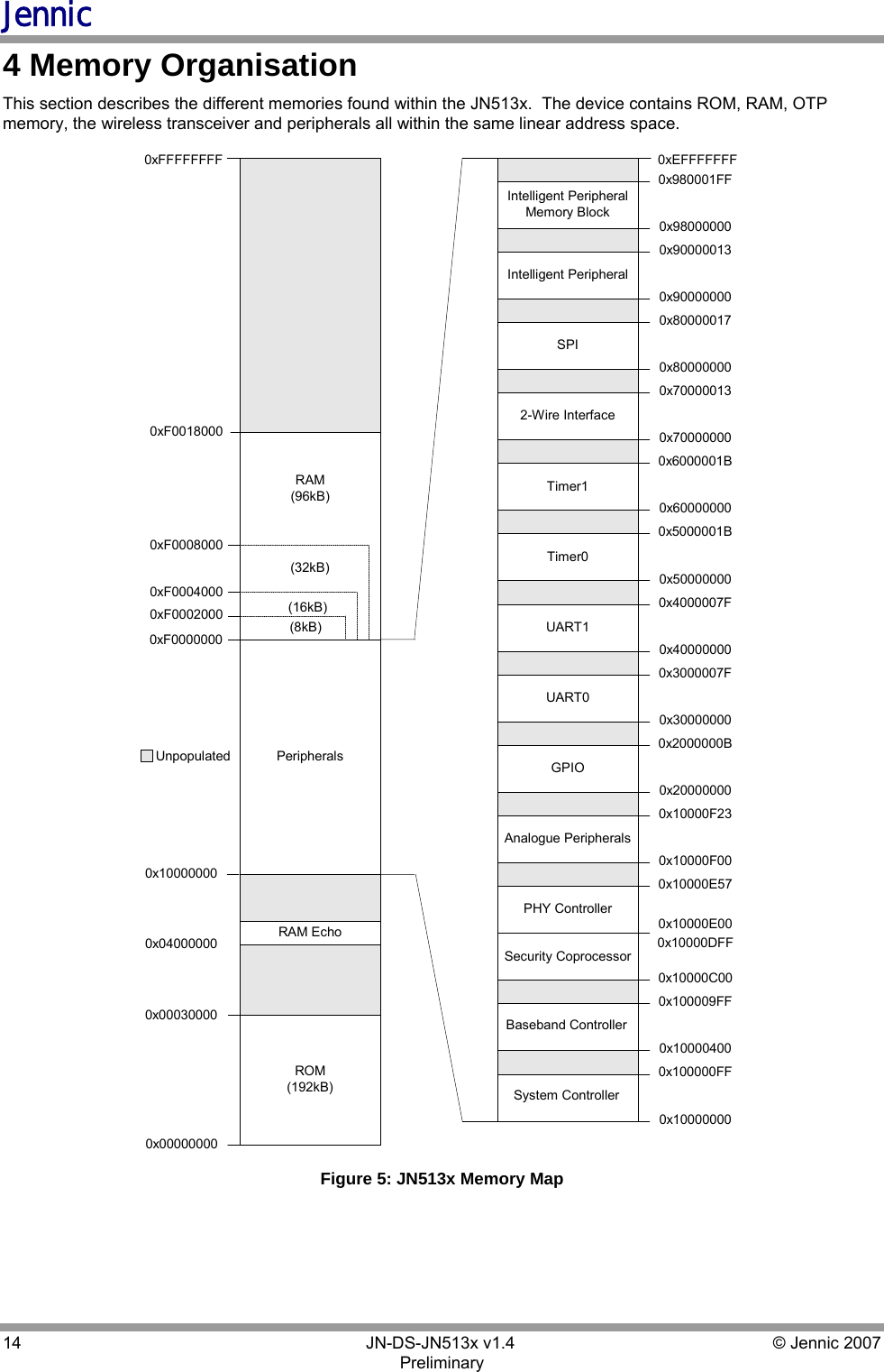
![Jennic © Jennic 2007 JN-DS-JN513x v1.4 15 Preliminary 4.1 ROM The ROM is 192K bytes in size, organized as 48k x 32-bit words and can be accessed by the CPU in a single clock cycle. The ROM contents change for different versions of the device to support differing protocol stacks and applications, all versions carry a default interrupt vector table and interrupt manager. Variants that can be used for application or protocol development carry a boot loader, to allow code from external Flash memory to be bootloaded into RAM at runtime. The operation of the boot loader is described in detail in Application Note JN-AN-1003 Boot Loader Operation [4]. For development variants the interrupt manager routes interrupt calls to the application’s soft interrupt vector table contained within RAM. Section 7 contains further information regarding the handling of interrupts. Typical ROM contents for a development variant containing a ZigBee protocol stack is shown in Figure 6. Interrupt VectorsInterrupt ManagerBoot LoaderIEEE802.15.4Stack0x000000000x00000F000x0002FFFFZigBee StackUnused Figure 6: Typical ROM contents 4.2 RAM The JN513x contains 8k, 16k, 32k or 96k bytes of high speed RAM organized as 2k, 4k, 8k or 24k x 32-bit words respectively. It can be used for both code and data storage and is accessed by the CPU in a single clock cycle. At reset, a boot loader controls the loading of segments of code and data from an external memory connected to the SPI port, into RAM. Software can control the power supply to the RAM allowing the contents to be maintained during a sleep period when other parts of the device are un-powered. 4.3 OTP eFuse Memory The JN513x contains 48-bytes of eFuse memory; this is one time programmable memory that is organised as 12 x 32-bit words, 4 words are reserved by Jennic, 2 of which support on-chip MAC ID. The remaining 8 words are fully user programmable, designed to allow the storage of configuration and product information. If secure external memory encryption is enabled then 4 words of the user eFuse are used for this (see section 4.4.1) At a low level, programming of the eFuse requires a sequence of carefully controlled steps, therefore to simplify the procedure, a simple API function call through software is provided that handles the various sequences required, this is described in JN-RM-2001 Integrated Peripherals API [2]. For reliable programming operation, a minimum system supply voltage VDD2 of 3.6V must be provided. If this condition is not satisfied, then programming reliability cannot be guaranteed. 4.4 External Memory An external memory with an SPI interface may be used to provide storage for program code and data for the device when external power is removed. The memory is connected to the SPI interface using select line SPISEL0; this](https://usermanual.wiki/NXP-Laboratories-UK/JN5139M4.Manual/User-Guide-933298-Page-15.png)
![Jennic 16 JN-DS-JN513x v1.4 © Jennic 2007 Preliminary select line is dedicated to the external memory interface and is not available for use with other external devices. See Figure 7 for connection details. JN513x SerialMemorySPISEL0SPIMISOSPIMOSISPICLKSSSDOSDICLK Figure 7: Connecting External Serial Memory At reset, the contents of this memory are copied into RAM by the software boot loader. A number of types of memory device may be used with the JN513x boot loader so long as they conform to the format of read instructions issued by the boot loader over the SPI interface. See application note [4] JN-AN-1003 Boot Loader Operation for details on the format of the read command and other details of the boot loader. 4.4.1 Secure External Memory Encryption The contents of the external serial memory may be securely encrypted to protect against system cloning or intrusion. The AES security processor combined with a user programmable 128-bit encryption key is used to encrypt the contents of the external memory. The encryption key is stored in eFuse and is programmed through software control. Initially after programming, the encryption feature is not active; this allows the system to continue to operate in an unsecured mode. Enabling of the encryption feature is through software control, once enabled all programming operations require authentication. Full details of the eFuse software functions may be found in JN-RM-2001 Integrated Peripherals API [2]. When bootloading program code from external serial memory, the JN513x automatically accesses the encryption key to execute the decryption process. User program code, does not need to handle any of the decryption process, it is a transparent process. 4.5 Peripherals All peripherals have their registers mapped into the memory space. Access to these registers requires 3 clock cycles. Applications have access to the peripherals through the peripherals library, which presents a high-level view of the peripheral’s functions through a series of dedicated software routines. These routines provide both a tested method for using the peripherals and operation of power and interrupts with the IEEE802.15.4 software protocol stack allowing bug-free application code to be developed more rapidly. See JN-RM-2001 Integrated Peripherals API [2] for more details. 4.6 Unused Memory Addresses Any attempt to access an unpopulated memory area will result in a bus error exception (interrupt) being generated.](https://usermanual.wiki/NXP-Laboratories-UK/JN5139M4.Manual/User-Guide-933298-Page-16.png)
![Jennic 18 JN-DS-JN513x v1.4 © Jennic 2007 Preliminary 6 Reset A system reset initialises the device to a predefined state and forces the CPU to start program execution from the reset vector. The reset process that the JN513x goes through is as follows. When power is applied, the 32kHz oscillator starts up and stabilises, which takes approximately 100μsec. At this point, the 16MHz crystal oscillator is enabled and power is applied to processor and peripheral logic. The logic blocks are held in reset until the 16MHz crystal oscillator stabilises, typically this takes 2.5ms. Once the oscillator is up and running the internal reset is removed from the CPU and peripheral logic and the CPU starts to run code beginning at the reset vector, consisting of initialisation code and then optionally the resident Boot Loader (described in reference [4]). Section 17.3.1 provides detailed electrical data and timing. The JN513x has four sources of reset: • Internal Power-on Reset • External Reset • Software Reset • Brown-Out-Detect Note: When the device exits a reset condition, device operating parameters (voltage, frequency, temperature, etc.) must be met to ensure operation. If these conditions are not met, then the device must be held in reset until the operating conditions are met. 6.1 Internal Power-on Reset For the majority of applications the internal power-on reset is capable of generating the required reset signal. When power is applied to the device, the power-on reset circuit monitors the rise of the VDD supply. When the VDD reaches the specified threshold, the reset signal is generated and can be observed as a rising edge on the RESETN pin. This signal is held internally until the power supply and oscillator stabilisation time has elapsed, when the internal reset signal is then removed and the CPU is allowed to run. RESETN PinInternal RESETVDD Figure 9: Internal Power-on Reset](https://usermanual.wiki/NXP-Laboratories-UK/JN5139M4.Manual/User-Guide-933298-Page-18.png)
![Jennic 20 JN-DS-JN513x v1.4 © Jennic 2007 Preliminary external sensors). The reset output feature can be enabled or disabled for the software generated reset using the function vAHI_DriveResetOut()within the peripheral library (the default state is disabled). 6.4 Brown-out Detect A brown-out detect module is used to monitor the supply voltage to the JN513x; this can be used whilst the device is awake or is in CPU doze mode. Dips in the supply voltage below a variable threshold can be detected and can be used to cause the JN513x to perform a chip reset. Equally, dips in the supply voltage can be detected and used to cause an interrupt to the processor, when the voltage either drops below the threshold or rises above it. Hysteresis is built into the brown out detect module this is nominally 100mV. The threshold voltage is selectable at levels of 2.1V, 2.4V, 2.5V or 2.6V through software control, this is described in JN-RM-2001 Integrated Peripherals API [2].](https://usermanual.wiki/NXP-Laboratories-UK/JN5139M4.Manual/User-Guide-933298-Page-20.png)
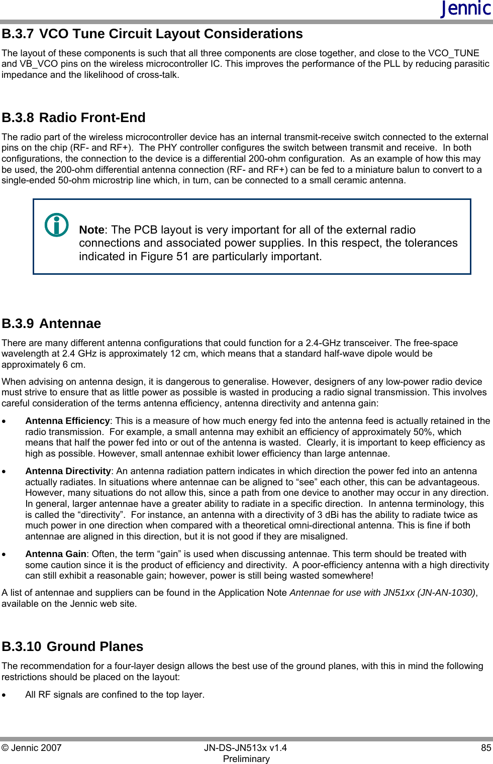
![Jennic © Jennic 2007 JN-DS-JN513x v1.4 23 Preliminary 8 Wireless Transceiver The wireless transceiver comprises a 2.45GHz radio, an O-QPSK modem, a baseband processor, a security coprocessor and PHY controller. These blocks, with protocol software provided as a library, implement an IEEE802.15.4 standards-based wireless transceiver that transmits and receives data over the air in the unlicensed 2.4GHz band. IEEE802.15.4 wireless functionality is provided with the transceiver and the protocol software described in JN-RM-2002 802.15.4 Stack [3]. Applications interface to the protocol software via an API interface that corresponds to the SAP interfaces defined in the IEEE Std 802.15.4-2006 [1] 8.1 Radio IDATAQDATAIF DATAAGCDACDACPAPAPowerPA (I)TrimPA (Q)Trim∑CalibrationReference& BIASADCLNATXRXVGA2VGA1VGAVGAPLL900LOILOQLOILOQLOILOQCalibrationVCO Figure 13: Radio Architecture The radio comprises a low-IF receive path and a direct up-conversion transmit path, which converge at the TX/RX switch. This switch includes the necessary matching components such that a 200Ω differential antenna may be directly connected without external components. Alternatively, a balun can be used for single ended antennas. The 16MHz crystal oscillator feeds a divider, which provides the frequency synthesiser with a reference frequency. The synthesiser contains programmable feedback dividers, phase detector, charge pump and internal Voltage Controlled Oscillator (VCO). The VCO has no external components, and includes calibration circuitry to compensate for differences in internal component values due to process and temperature variations. The VCO is controlled by a Phase Lock Loop (PLL) that has a loop filter comprising 3 external components. A programmable charge pump is also used to tune the loop characteristic. Finally, quadrature (I and Q) local oscillator signals for the mixer drives are derived. The receiver chain starts with the low noise amplifier / mixer combination whose outputs are passed to the polyphase bandpass filter. This filter provides the channel definition as well as image frequency rejection. The signal is then passed to two variable gain amplifier blocks. The gain control for these stages, and the bandpass filter, is derived in the automatic gain control (AGC) block within the Modem. The signal is conditioned with the anti-alias low pass filter, before being converted to a digital signal with a flash ADC. In the transmit direction, the digital I and Q streams from the Modem are passed to I and Q quadrature DAC blocks which are buffered and low-pass filtered, before being applied to the modulator mixers. The summed 2.4 GHz signal is then passed to the RF Power Amplifier (PA), whose power control can be selected from one of six settings. The output of the PA drives the antenna via the RX/TX switch.](https://usermanual.wiki/NXP-Laboratories-UK/JN5139M4.Manual/User-Guide-933298-Page-23.png)

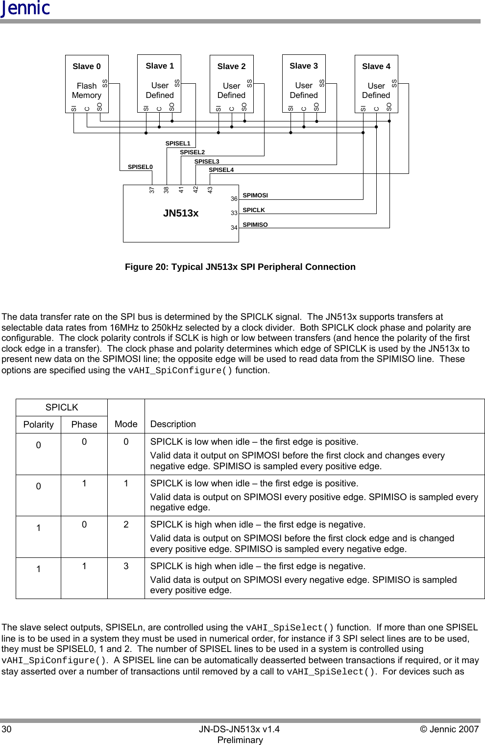
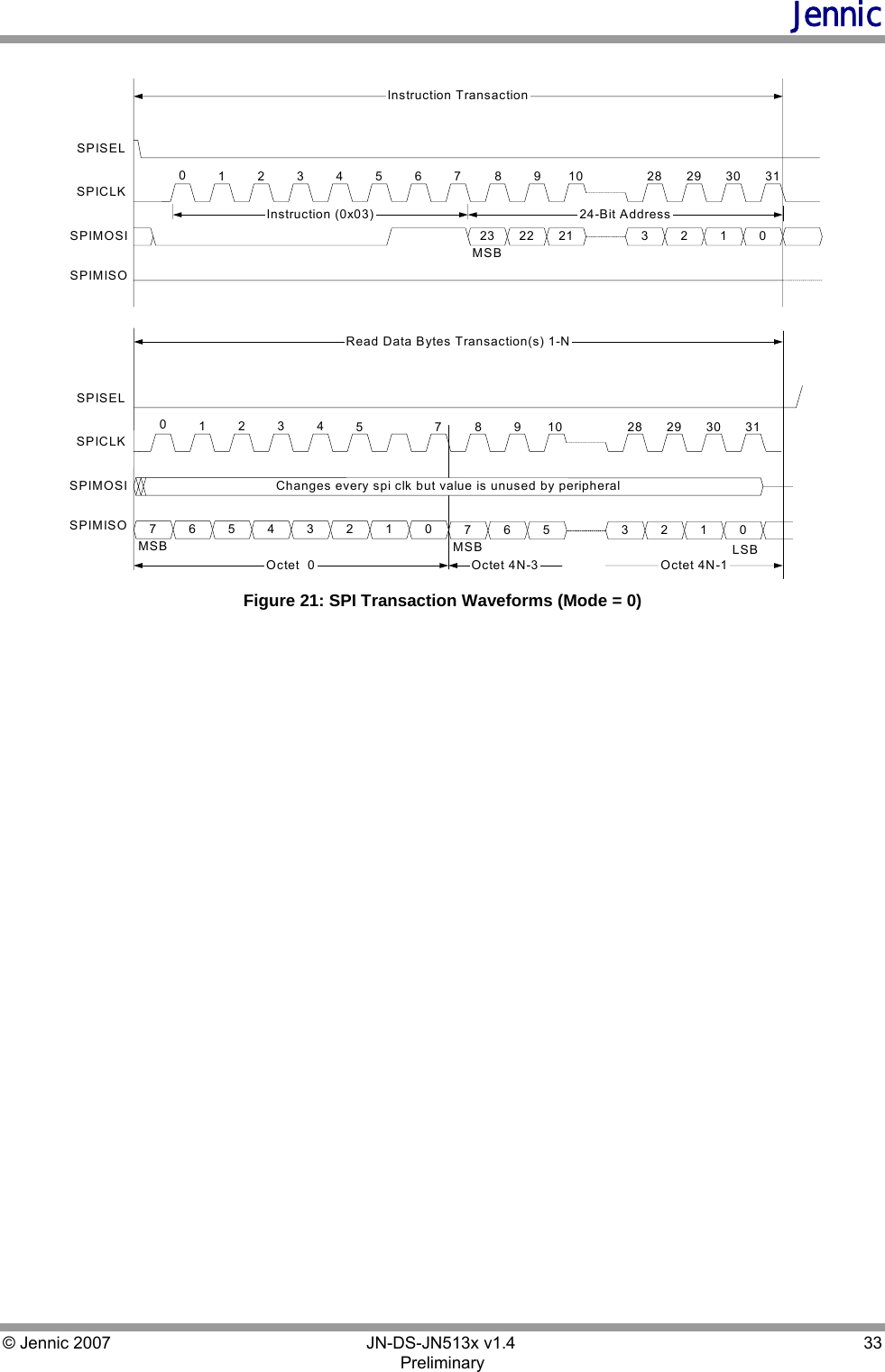
![Jennic © Jennic 2007 JN-DS-JN513x v1.4 29 Preliminary 10 Serial Peripheral Interface The Serial Peripheral Interface (SPI) allows high-speed synchronous data transfer between the JN513x and peripheral devices. The JN513x operates as a master on the SPI bus and all other devices connected to the SPI are expected to be slave devices under the control of the JN513x CPU. The SPI includes the following features: • Full-duplex, three-wire synchronous data transfer • Programmable bit rates up to 16Mbps • Programmable transaction size of 8,16 or 32 bits • Supports standard SPI modes 0, 1, 2, 3 to allow control over the relationship between clock and transmit / receive data • Automatic slave select generation (up to 5 slaves) • Maskable transaction complete interrupt • LSB First or MSB First Data Transfer ClockDividerSPI BusCycleControllerData Buffer31 15 7DIVClock EdgeSelectDataCHAR_LENLSBSPIMISOSPIMOSISPICLKSelectLatchSPISEL [4..0]16 MHz 0 Figure 19: SPI Block Diagram The SPI bus employs a simple shift register data transfer scheme. Data is clocked out of and into the active devices in a first-in, first-out fashion allowing SPI devices to transmit and receive data simultaneously. There are three dedicated pins SPICLK, SPIMOSI, SPIMISO that are shared across all devices on the bus. Master-Out-Slave-In or Master-In-Slave-Out data transfer is relative to the clock signal SPICLK generated by the JN513x. The JN513x provides five slave selects, SPISEL0 to SPISEL4 to allow five SPI peripherals on the bus. SPISEL0 is a dedicated pin and SPISEL1 to 4, are alternate functions of pins DIO0 to 3 respectively. This allows a serial flash memory to be connected to SPISEL0 and download to internal RAM via software from reset. The interface can transfer 8, 16 or 32 bits without software intervention and can keep the slave select lines asserted between transfers when required, to enable longer transfers to be performed.](https://usermanual.wiki/NXP-Laboratories-UK/JN5139M4.Manual/User-Guide-933298-Page-29.png)
![Jennic © Jennic 2007 JN-DS-JN513x v1.4 45 Preliminary JN513xCTSRTSRXDTXDUART0RS232LevelShifter123456789CDRDTDDTRSGDSRRTSCTSRIPC COM PortPin Signal156947464445 Figure 32 JN513x Serial Communication Link 13.3 Programming Example The following code shows the peripheral library calls to configure UART0 and output the message ‘Hello World’ Programming Example /* Set up uart0 */ vAHI_UartEnable(E_AHI_UART_0); /* set baud rate */ vAHI_UartSetClockDivisor(0, E_AHI_UART_RATE_38400); /* set parity, start bits, number data bits */ vAHI_UartSetControl(E_AHI_UART_0, E_AHI_UART_EVEN_PARITY, E_AHI_UART_PARITY_DISABLE, E_AHI_UART_WORD_LEN_8, E_AHI_UART_1_STOP_BIT, E_AHI_UART_RTS_HIGH); /* output message */ char acstring[] = “Hello World”; char *pcstring = acstring; while (*pcstring) { vAHI_UartWriteData(E_AHI_UART_0, *pcstring); pcstring++; }](https://usermanual.wiki/NXP-Laboratories-UK/JN5139M4.Manual/User-Guide-933298-Page-45.png)
![Jennic © Jennic 2007 JN-DS-JN513x v1.4 49 Preliminary Programming Example PRIVATE bool_t bSIFRead(uint8 u8SlaveAddress, uint8 *pau8ReadBuffer, uint32 u32Length) { int i; for (i=0; i<u32Length; i++) { /* set slave address */ vAHI_SiWriteSlaveAddr(u8SlaveAddress, E_AHI_SI_SLAVE_RW_SET); /* send read command */ vAHI_SiSetCmdReg(E_AHI_SI_START_BIT, E_AHI_SI_NO_STOP_BIT, E_AHI_SI_NO_SLAVE_READ, E_AHI_SI_SLAVE_WRITE, E_AHI_SI_SEND_ACK, E_AHI_SI_NO_IRQ_ACK); while(bAHI_SiPollTransferInProgress()); /* busy wait */ if (bAHI_SiPollArbitrationLost() | bAHI_SiPollRxNack()) { /* release bus & abort */ vAHI_SiSetCmdReg(E_AHI_SI_NO_START_BIT, E_AHI_SI_STOP_BIT, E_AHI_SI_NO_SLAVE_READ, E_AHI_SI_SLAVE_WRITE, E_AHI_SI_SEND_ACK, E_AHI_SI_NO_IRQ_ACK); return FALSE; } if (i < u32Length - 1) { /* read and ack */ vAHI_SiSetCmdReg(E_AHI_SI_NO_START_BIT, E_AHI_SI_NO_STOP_BIT, E_AHI_SI_SLAVE_READ, E_AHI_SI_NO_SLAVE_WRITE, E_AHI_SI_SEND_ACK, E_AHI_SI_NO_IRQ_ACK); } else /* last byte */ { /* read, stop, nack */ vAHI_SiSetCmdReg(E_AHI_SI_NO_START_BIT, E_AHI_SI_STOP_BIT, E_AHI_SI_SLAVE_READ, E_AHI_SI_NO_SLAVE_WRITE, E_AHI_SI_SEND_NACK, E_AHI_SI_NO_IRQ_ACK); } while(bAHI_SiPollTransferInProgress()); /* busy wait */ if (bAHI_SiPollArbitrationLost()) { /* release bus & abort */ vAHI_SiSetCmdReg(E_AHI_SI_NO_START_BIT, E_AHI_SI_STOP_BIT, E_AHI_SI_NO_SLAVE_READ, E_AHI_SI_NO_SLAVE_WRITE, E_AHI_SI_SEND_ACK, E_AHI_SI_NO_IRQ_ACK); return FALSE; } /* Store data read from device */ pau8ReadBuffer[i] = u8AHI_SiReadData8(); } /* transfer complete */ vAHI_SiSetCmdReg(E_AHI_SI_NO_START_BIT, E_AHI_SI_STOP_BIT, E_AHI_SI_NO_SLAVE_READ, E_AHI_SI_NO_SLAVE_WRITE, E_AHI_SI_SEND_ACK, E_AHI_SI_NO_IRQ_ACK); return TRUE; }](https://usermanual.wiki/NXP-Laboratories-UK/JN5139M4.Manual/User-Guide-933298-Page-49.png)
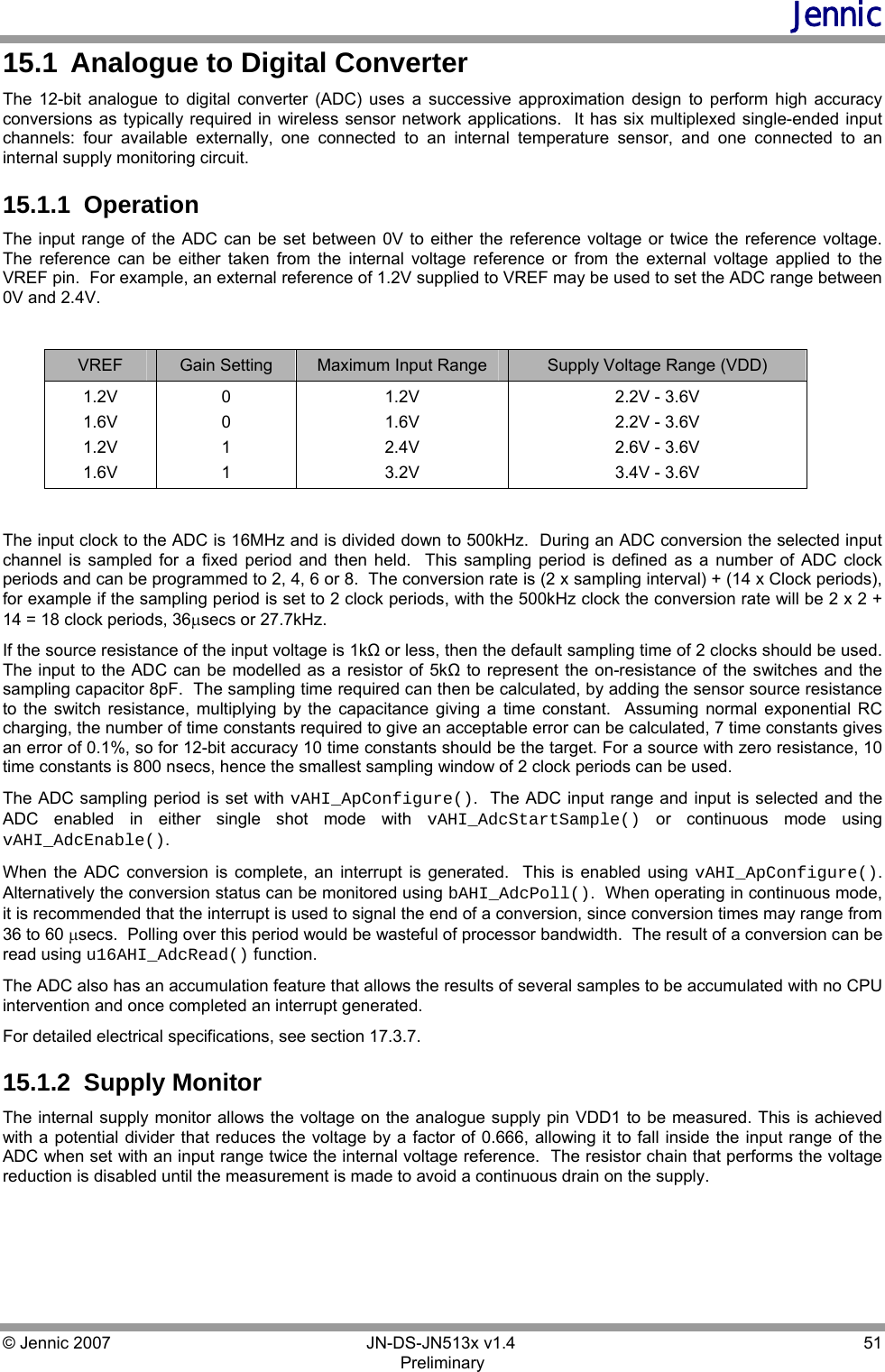
![Jennic 52 JN-DS-JN513x v1.4 © Jennic 2007 Preliminary 15.1.3 Temperature Sensor The on-chip temperature sensor can be used either to provide an absolute measure of the device temperature or to detect changes in the ambient temperature. In common with most on-chip temperature sensors, it is not trimmed and so the absolute accuracy variation is large; the user may wish to calibrate the sensor prior to use. The sensor forces a constant current through a forward biased diode to provide a voltage output proportional to the chip die temperature which can then be measured using the ADC. The measured voltage has a linear relationship to temperature as described in section 17.3.11. Because this sensor is on-chip, any measurements taken must account for the thermal time constants. For example if the device just came out of sleep mode the user application should wait until the temperature has stabilized before taking a measurement. 15.1.4 Programming Example The following example illustrates data logging using the ADC1 input channel. Programming Example PRIVATE void vAdcDataLogger(uint16 *pau16DataBuffer, uint32 u32Length) { int i; /* configure Analogue Peripheral timings, interrupt & ref voltage */ vAHI_ApConfigure( E_AHI_AP_REGULATOR_ENABLE, E_AHI_AP_INT_DISABLE, E_AHI_AP_SAMPLE_2, E_AHI_AP_CLOCKDIV_500KHZ, E_AHI_AP_INTREF); while (!bAHI_APRegulatorEnabled); /* configure & enable DAC */ vAHI_AdcEnable(E_AHI_ADC_CONVERT_ENABLE, E_AHI_AP_INPUT_RANGE_1, E_AHI_ADC_SRC_ADC_1); while(TRUE) { for (i=0;i<u32Length;i++) { vAHI_AdcStartSample(); /* start capture */ while(bAHI_AdcPoll()); /* busy wait until capture complete */ pau16DataBuffer[i] = u16AHI_AdcRead(); /* store in buffer */ } } } 15.2 Digital to Analogue Converter The Digital to Analogue Converter (DAC) provides two output channels and is capable of producing voltages of 0 to Vref or 0 to 2Vref where Vref is selected between the internal reference and the VREF pin, with a resolution of 11 bits and a minimum conversion time of 9μsecs (2MHz clock). 15.2.1 Operation The output range of each DAC can be set independently to swing between 0V to either the reference voltage or twice the reference voltage. The reference voltage is selected from the internal reference or the VREF pin. For example, an external reference of 0.8V supplied to VREF may be used to set DAC1 maximum output of 0.8V and DAC2 maximum output of 1.6V.](https://usermanual.wiki/NXP-Laboratories-UK/JN5139M4.Manual/User-Guide-933298-Page-52.png)
![Jennic 56 JN-DS-JN513x v1.4 © Jennic 2007 Preliminary the output values, and this therefore preserves any interface to the outside world. The DAC outputs are placed into a high impedance state. When entering into sleep mode, there is an option to retain the RAM contents throughout the sleep period, this is determined by vAHI_MemoryHold(). If wakeup timers or comparator event are not to be used for a wakeup event, then power can be saved by switching off the 32kHz oscillator through software control. Whilst in sleep mode one of three possible events can cause a wakeup to occur, transitions on DIO inputs, expiry of wakeup timers or comparator events. If any of these events occur, an interrupt is generated that will cause a wakeup from sleep. It is possible for multiple wakeup sources to trigger an event at the same instant and only one of them will be accountable for the wakeup period. It is therefore necessary in software to remove all other pending wakeup events prior to requesting entry back into sleep mode; otherwise, the device will re-awaken immediately. When wakeup occurs, a similar sequence of events to the reset process described in section 6.1 happens. The 16MHz oscillator is started up, once stable the power to CPU system is enabled and the reset is removed. Software determines that this is a reset from sleep and so commences with the wakeup process. 16.3.1 Wakeup Timer Event The JN513x contains two 32-bit wakeup timers that are counters clocked from the 32kHz oscillator, and can be programmed to generate a wake-up event. Following a wakeup event, the timers continue to run. These timers are described in section 12.3. Timer events can be generated from both of the two timers; one is intended for use by the 802.15.4 protocol, the other being available for use by the Application running on the CPU. These timers are available to run at any time, even during sleep mode, and are controlled by API calls as detailed in the Jennic document JN513x JN-RM-2001 Integrated Peripherals API [2]. 16.3.2 DIO Event Any DIO pin when used as an input has the capability, by detecting a transition, to generate a wake-up event. Once this feature has been enabled using the vAHI_DioInterruptEnable() function the type of transition can be specified (rising or falling edge) by using the vAHI_DioInterruptEdge() function. Even when groups of DIO lines are configured as alternative functions such as the UARTs or Timers etc, any input line in the group can still be used to provide a wakeup event. This means that an external device communicating over the UART can wakeup a sleeping device by asserting its RTS signal pin. 16.3.3 Comparator Event The comparator can generate a wakeup interrupt when a change in the relative levels of the positive and negative inputs occurs, the negative input being selectable between the external pin COMPxN or the internal voltage reference. The ability to wakeup when continuously monitoring analogue signals is useful in ultra-low power applications. The JN513x can remain in sleep mode until the voltage drops below a threshold and then be woken up to deal with the alarm condition. 16.4 Deep Sleep Mode Deep sleep mode gives the lowest power consumption. All switchable power domains are off and certain functions in the VDD supply power domain, including the 32kHz oscillator are stopped. It is entered by executing the vAHI_PowerDown() function. This mode can be exited by a power down, a hardware reset on the RESETN pin, or a DIO event. The DIO event in this mode causes a chip reset to occur.](https://usermanual.wiki/NXP-Laboratories-UK/JN5139M4.Manual/User-Guide-933298-Page-56.png)
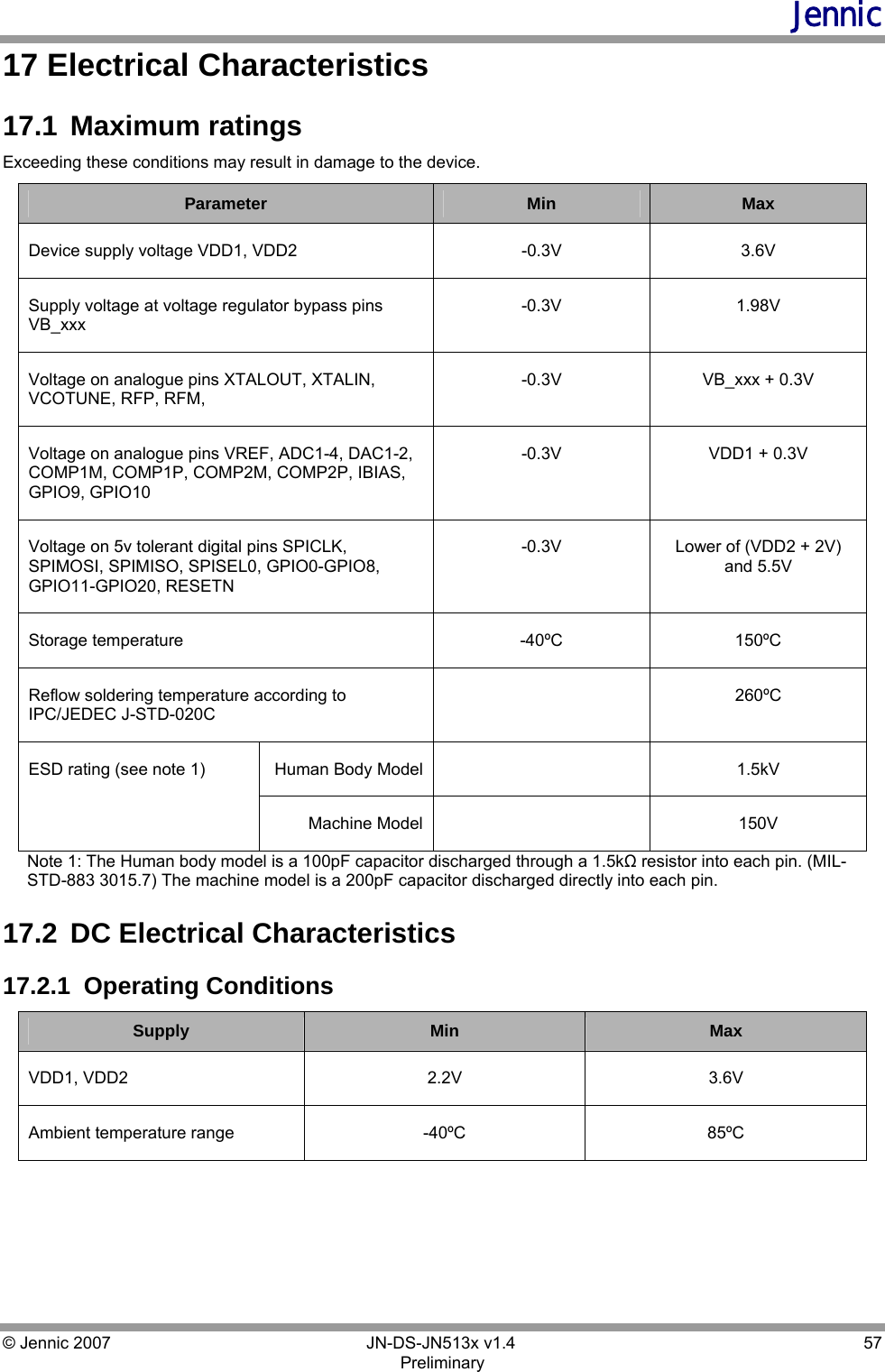
![Jennic 58 JN-DS-JN513x v1.4 © Jennic 2007 Preliminary 17.2.2 DC Current Consumption VDD = 2.2 to 3.6V, -40 to +85º C 17.2.2.1 Active Processing Mode: Min Typ Max Unit Notes CPU processing 2.7 + 0.325/MHz mA SPI, GPIOs enabled CPU processing (2 x clock) 2.7 + 0.325/MHz mA SPI, GPIOs enabled Radio transmit [boost mode] 34 [38] mA CPU in software doze – radio transmitting Radio receive [boost mode] 34 [37] mA CPU in software doze – radio in receive mode The following current figures should be added to those above if the feature is being used ADC 580 µA Temperature sensor and battery measurements require ADC DAC 220 / 250 µA One / both Comparator 67 / 1.2 µA Fast response time / low-power UART 110 µA For each UART Timer 65 µA For each Timer 2-wire serial interface 86 µA 17.2.2.2 Sleep Mode Mode: Min Typ Max Unit Notes Sleep mode with I/O wakeup 0.2 µA Waiting on I/O event. Sleep mode with I/O and timer wakeup 1.3 µA As above, but also waiting on timer event. If both wakeup timers are enabled then add another 0.3µA The following current figures should be added to those above if the feature is being used RAM retention 2.0 µA For full 96kB retained. Comparator (low-power mode) 1.2 µA Reduced response time. 17.2.2.3 Deep Sleep Mode Mode: Min Typ Max Unit Notes Deep sleep mode 0.2 0.4 µA Waiting on chip RESET or I/O event.](https://usermanual.wiki/NXP-Laboratories-UK/JN5139M4.Manual/User-Guide-933298-Page-58.png)
![Jennic © Jennic 2007 JN-DS-JN513x v1.4 67 Preliminary 17.3.12.1 Radio parameters: 2.2-3.6V, +25ºC Parameter Min Typical Max Unit Notes Receiver Characteristics Receive sensitivity -95.5 dBm Nominal for 1% PER, as per 802.15.4 section 6.5.3.3 Receive sensitivity (boost) -96.5 dBm Nominal for 1% PER, as per 802.15.4 section 6.5.3.3 Maximum input signal 0 dBm For 1% PER, measured as sensitivity Adjacent channel rejection -1 channel / +1 channel [CW Interferer] 31 / 33 [35 / 38] dB For 1% PER with wanted signal 3dB above sensitivity, as per 802.15.4 section 6.5.3.4 (modulated interferer) Alternate channel rejection [CW Interferer] 41 [45] dB For 1% PER with wanted signal 3dB above sensitivity, as per 802.15.4 section 6.5.3.4 (modulated interferer) Other in band rejection 2.4 to 2.4835 GHz, excluding adj channels 46 dB For 1% PER with wanted signal 3dB above sensitivity, measured as per 802.15.4 section 6.5.3.4 Out of band rejection >45 dB Spurious emissions (RX) -57 -47 dBm 30MHz to 1GHz 1GHz to 12GHz Intermodulation protection 40 dB For 1% PER at with wanted signal 3dB above sensitivity. Modulated Interferers at 2 & 4 channel separation RSSI linearity -3 +3 dB -95 to -10dBm. Available through Hardware API Transmitter Characteristics Transmit power 0.5 dBm Nominal Transmit power (boost) +2.5 dBm Output power control range -30 dB in 5 6dB steps Spurious emissions (TX) -36 -43 -47 dBm 30MHz to 1GHz, 1GHz to12.5GHz, The following exceptions apply 1.8 to 1.9GHz & 5.15 to 5.3GHz EVM 15 25 % At maximum output power Transmit Power Spectral Density -48 -20 dBc At greater than 3.5MHz offset, as per 802.15.4, section 6.5.3.1](https://usermanual.wiki/NXP-Laboratories-UK/JN5139M4.Manual/User-Guide-933298-Page-67.png)

![Jennic 80 JN-DS-JN513x v1.4 © Jennic 2007 Preliminary This can be used to give an equation for the required transconductance. 21221212])([4TTTTTTSmmCC CCCCCRg××++×≥ω Example: Using typical parameters of mR=40Ω, SC=1pF and 1TC=2TC=18pF ( for a load capacitance of 9pF), the equation above gives the required transconductance ( mg) as 647uA/V. The JN513x has a typical value for transconductance of 1.25mA/V The example and equation illustrate the trade-off that exists between the load capacitance and crystal ESR. For example, a crystal with a higher load capacitance can be used, but the value of max. ESR that can be tolerated is reduced. Also note, that the circuit sensitivity to external capacitance [ C1 , C2 ] is a square law. Below is measurement data showing the variation of the crystal oscillator amplifier transconductance with temperature and supply voltage, notice how small the variation is. Circuit techniques have been used to apply compensation, such that the user need only design for nominal conditions. Crystal Oscillator Transconductance Versus Temperature (VDD=3V)1.2451.251.2551.261.2651.271.2751.281.285-40 -20 0 20 40 60 80 100Temperature (C)Transconductance (mA/V) Crystal Oscillator Transconductance Versus Supply Voltage (Temp=25C)1.21.221.241.261.281.31.322.2 2.4 2.6 2.8 3.0 3.2 3.4 3.6Supply Voltage (VDD)Transconductance (mA/V)](https://usermanual.wiki/NXP-Laboratories-UK/JN5139M4.Manual/User-Guide-933298-Page-80.png)
![Jennic 90 JN-DS-JN513x v1.4 © Jennic 2007 Preliminary Appendix C Related Documents [1] IEEE Std 802.15.4-2003 IEEE Standard for Information technology – Part 15.4 Wireless Medium Access Control (MAC) and Physical Layer (PHY) Specifications for Low-Rate Wireless Personal Area Networks (LR-WPANs) [2] JN-RM-2001 Integrated Peripherals API [3] JN-RM-2002 802.15.4 Stack API [4] JN-AN-1003 Boot Loader Operation RoHS Compliance JN513x devices meet the requirements of Directive 2002/95/EC of the European Parliament and of the Council on the Restriction of Hazardous Substance (RoHS). Status Information The status of this Data Sheet is Preliminary. Jennic products progress according to the following format: Advanced The Data Sheet shows the specification of a product in planning or in development. The functionality and electrical performance specifications are target values and may be used as a guide to the final specification. Integrated circuits are identified with an R suffix, for example JN5139-Z01R. Jennic reserves the right to make changes to the product specification at anytime without notice. Preliminary The Data Sheet shows the specification of a product that is in production, but is not yet fully qualified. The functionality of the product is final. The electrical performance specifications are target values and may used as a guide to the final specification. Integrated circuits are identified with an R suffix, for example JN5139-Z01R. Jennic reserves the right to make changes to the product specification at anytime without notice. Production This is the final Data Sheet for the product. All functional and electrical performance specifications, including minimum and maximum values are final. This Data Sheet supersedes all previous document versions. Jennic reserves the right to make changes to the product specification at anytime to improve its performance.](https://usermanual.wiki/NXP-Laboratories-UK/JN5139M4.Manual/User-Guide-933298-Page-90.png)