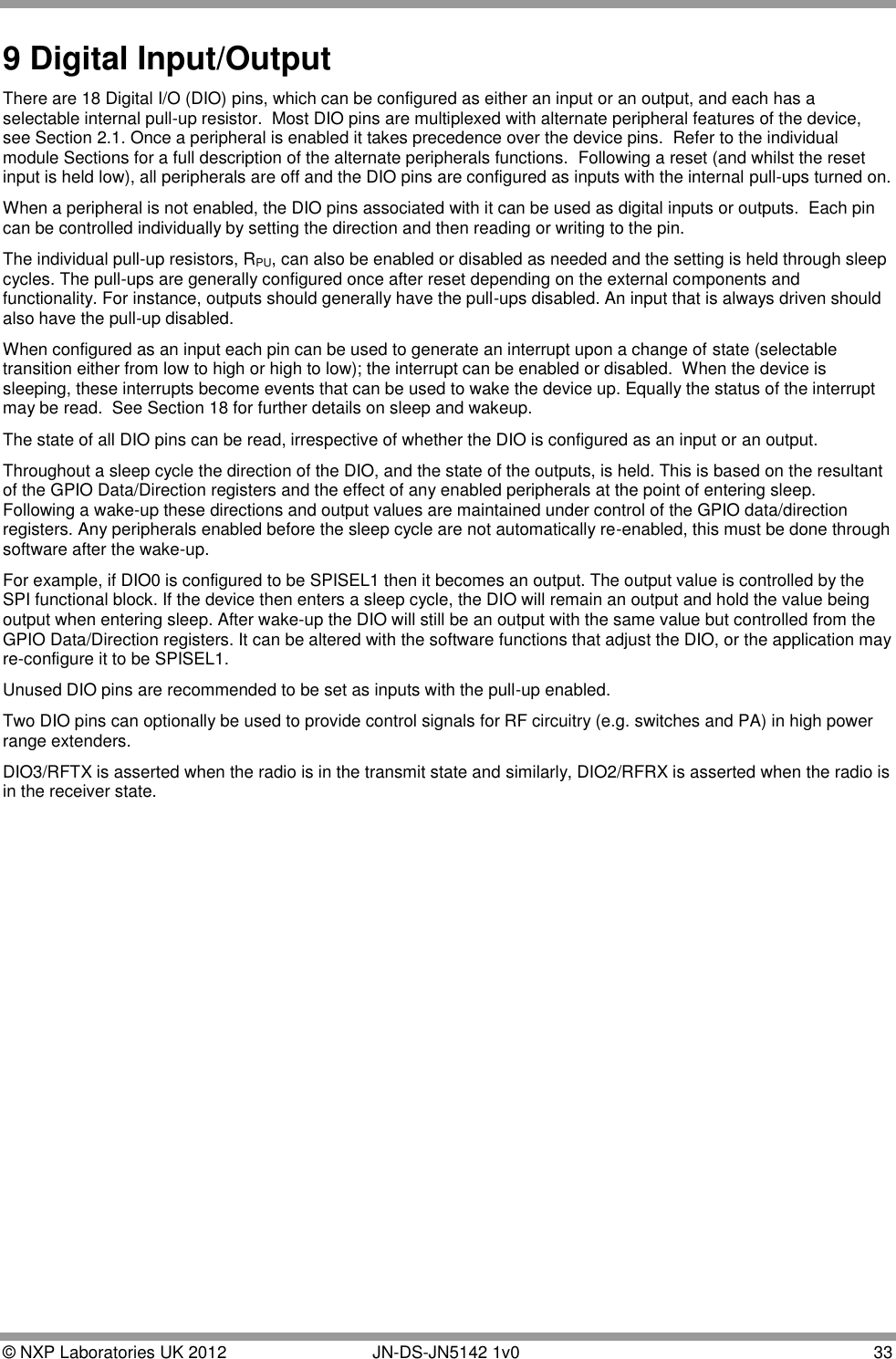
NXP Laboratories UK JN5142M0 JN5142-001-M00 IEEE802.15.4 Wireless Module User Manual JN DS JN5142
NXP Laboratories UK Ltd JN5142-001-M00 IEEE802.15.4 Wireless Module JN DS JN5142
UserManual.wiki
>
NXP Laboratories UK
>
JN5142M0 User Manual
>
Datasheet
Contents
1.
Datasheet
2.
User Datasheet
3.
Antenna Datasheet
Datasheet
Navigation menu
Upload a User Manual
Namespaces
Wiki Guide
HTML
PDF
Info
Views
User Manual
Discussion / Help
Navigation

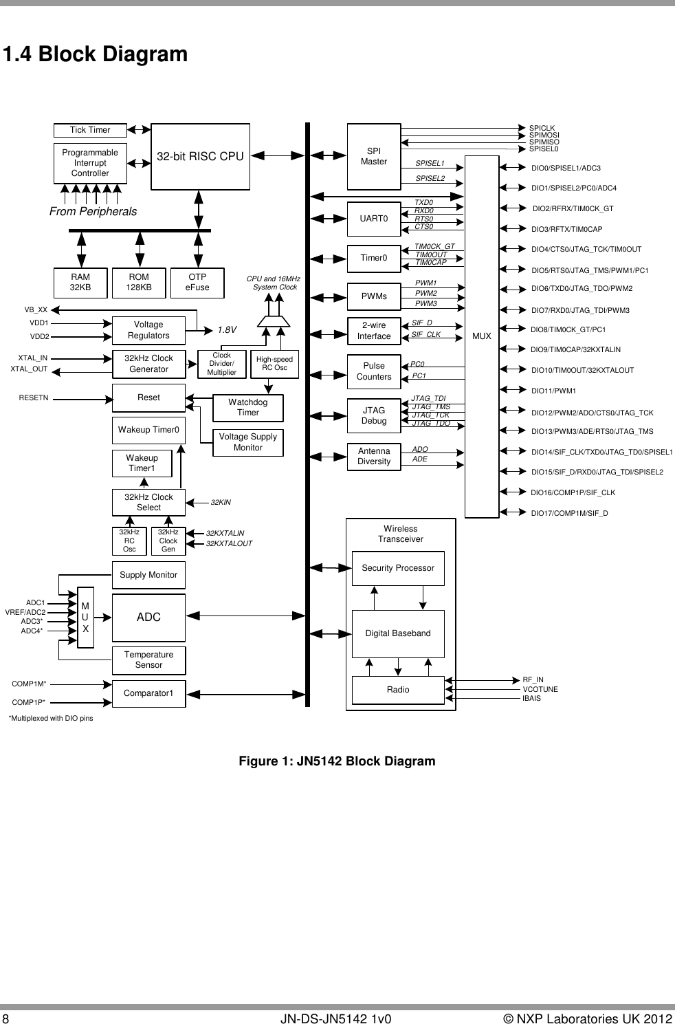
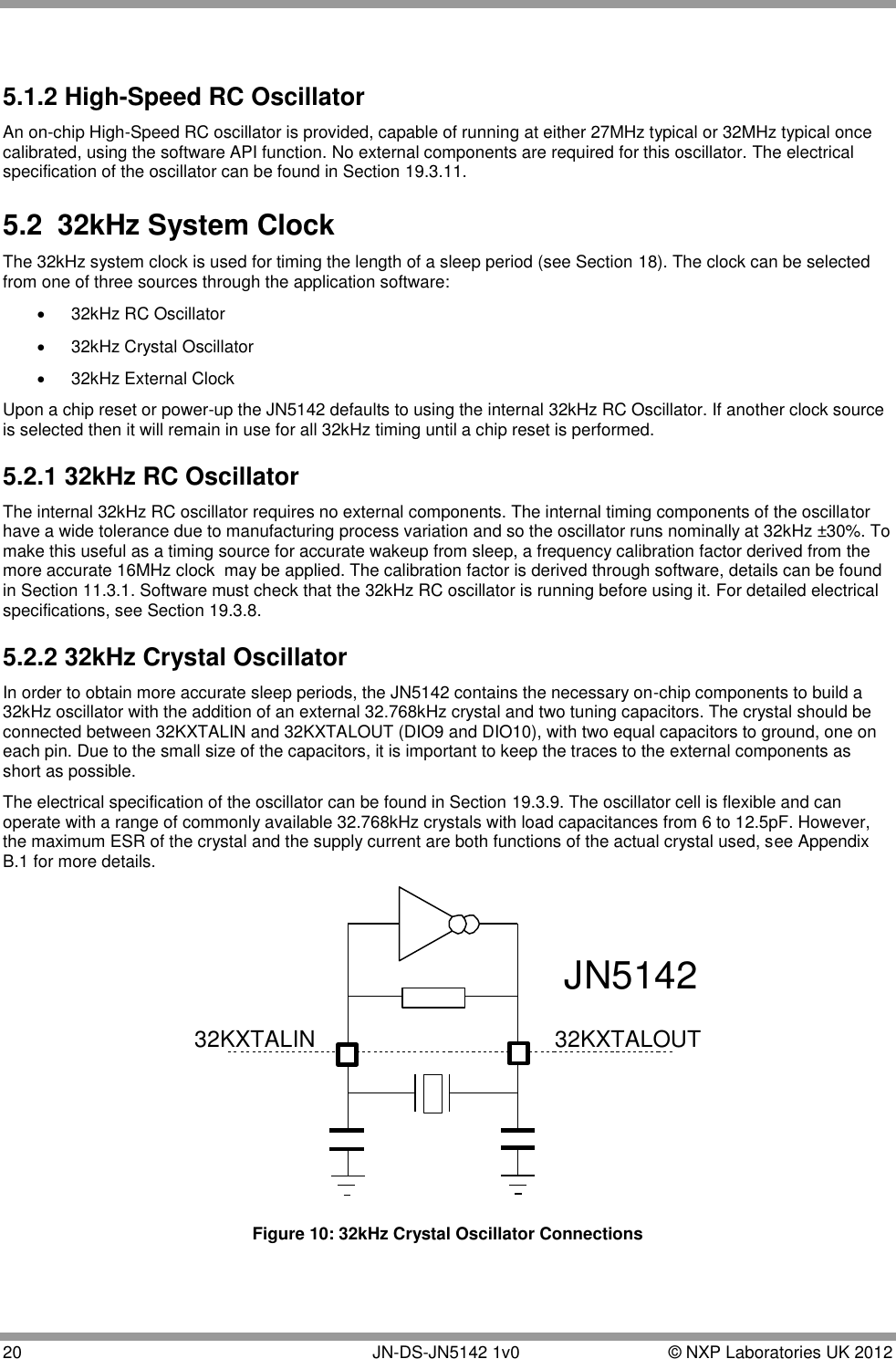
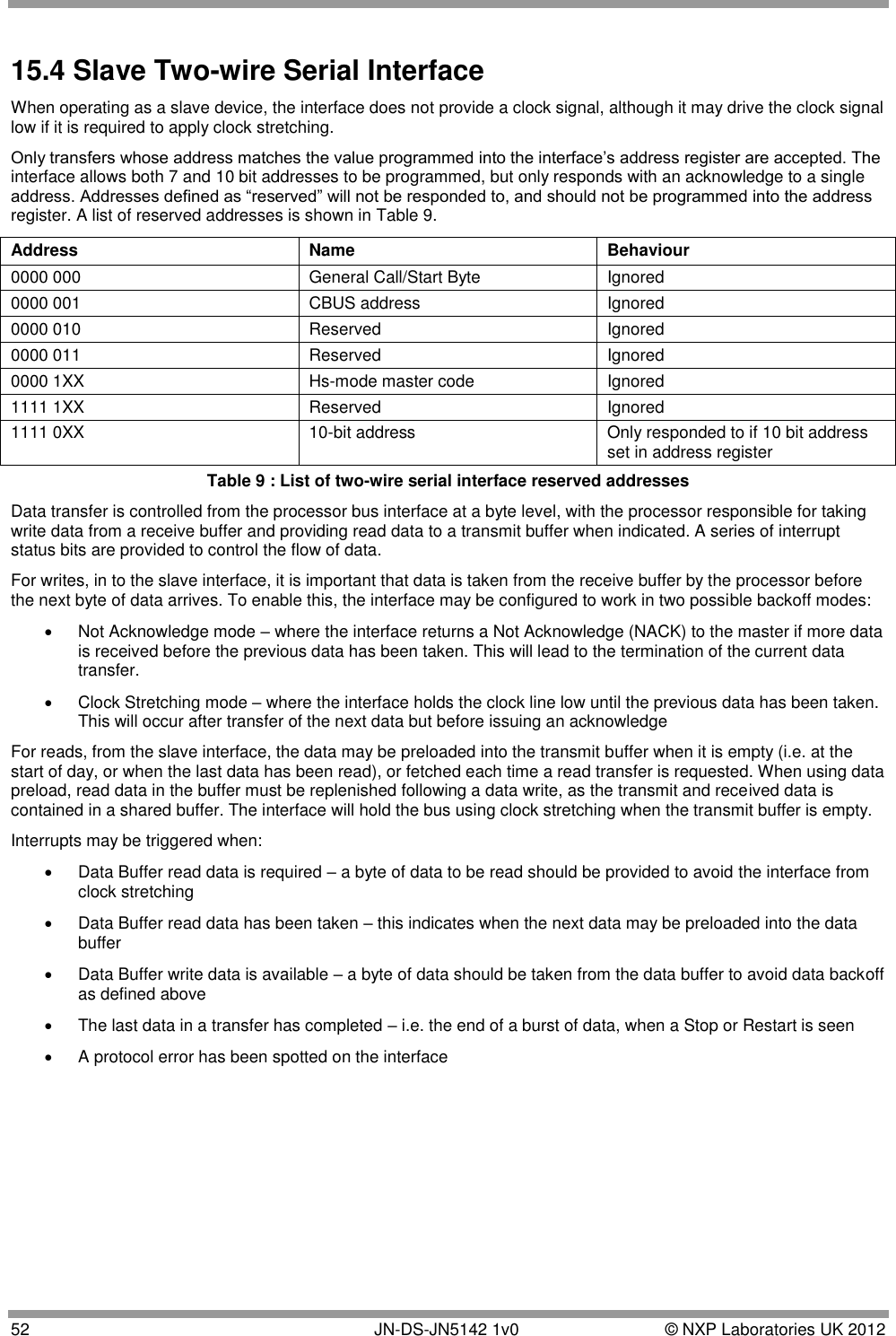
![6 JN-DS-JN5142 1v0 © NXP Laboratories UK 2012 1 Introduction The JN5142 is an IEEE802.15.4 wireless microcontroller that provides a fully integrated solution for applications using the IEEE802.15.4 standard in the 2.4 - 2.5GHz ISM frequency band [1], including RF4CE. A ROM variant provides support for JenNet-IP “Smart Device” applications such as lighting and building automation. Applications that transfer data wirelessly tend to be more complex than wired ones. Wireless protocols make stringent demands on frequencies, data formats, timing of data transfers, security and other issues. Application development must consider the requirements of the wireless network in addition to the product functionality and user interfaces. To minimise this complexity, NXP provides a series of software libraries and interfaces that control the transceiver and peripherals of the JN5142. These libraries and interfaces remove the need for the developer to understand wireless protocols and greatly simplifies the programming complexities of power modes, interrupts and hardware functionality. In view of the above, it is not necessary to provide the register details of the JN5142 in the datasheet. The device includes a Wireless Transceiver, RISC CPU, on chip memory and an extensive range of peripherals. 1.1 Wireless Transceiver The Wireless Transceiver comprises a 2.45GHz radio, a modem, a baseband controller and a security coprocessor. In addition, the radio also provides an output to control transmit-receive switching of external devices such as power amplifiers allowing applications that require increased transmit power to be realised very easily. Appendix B.4, describes a complete reference design including Printed Circuit Board (PCB) design and Bill Of Materials (BOM). The security coprocessor provides hardware-based 128-bit AES-CCM* modes as specified by the IEEE802.15.4 2006 standard. Specifically this includes encryption and authentication covered by the MIC –32/-64/-128, ENC and ENC-MIC –32/-64/-128 modes of operation. The transceiver elements (radio, modem and baseband) work together to provide IEEE802.15.4 (2006) MAC and PHY functionality under the control of a protocol stack. Applications incorporating IEEE802.15.4 functionality can be developed rapidly by combining user-developed application software with a protocol stack library. 1.2 RISC CPU and Memory A 32-bit RISC CPU allows software to be run on-chip, its processing power being shared between the IEEE802.15.4 MAC protocol, other higher layer protocols and the user application. The JN5142 has a unified memory architecture, code memory, data memory, peripheral devices and I/O ports are organised within the same linear address space. The device contains 128kbytes of ROM, 32kbytes of RAM and a 29-byte One Time Programmable (OTP) eFuse memory.](https://usermanual.wiki/NXP-Laboratories-UK/JN5142M0.Datasheet/User-Guide-1655318-Page-6.png)

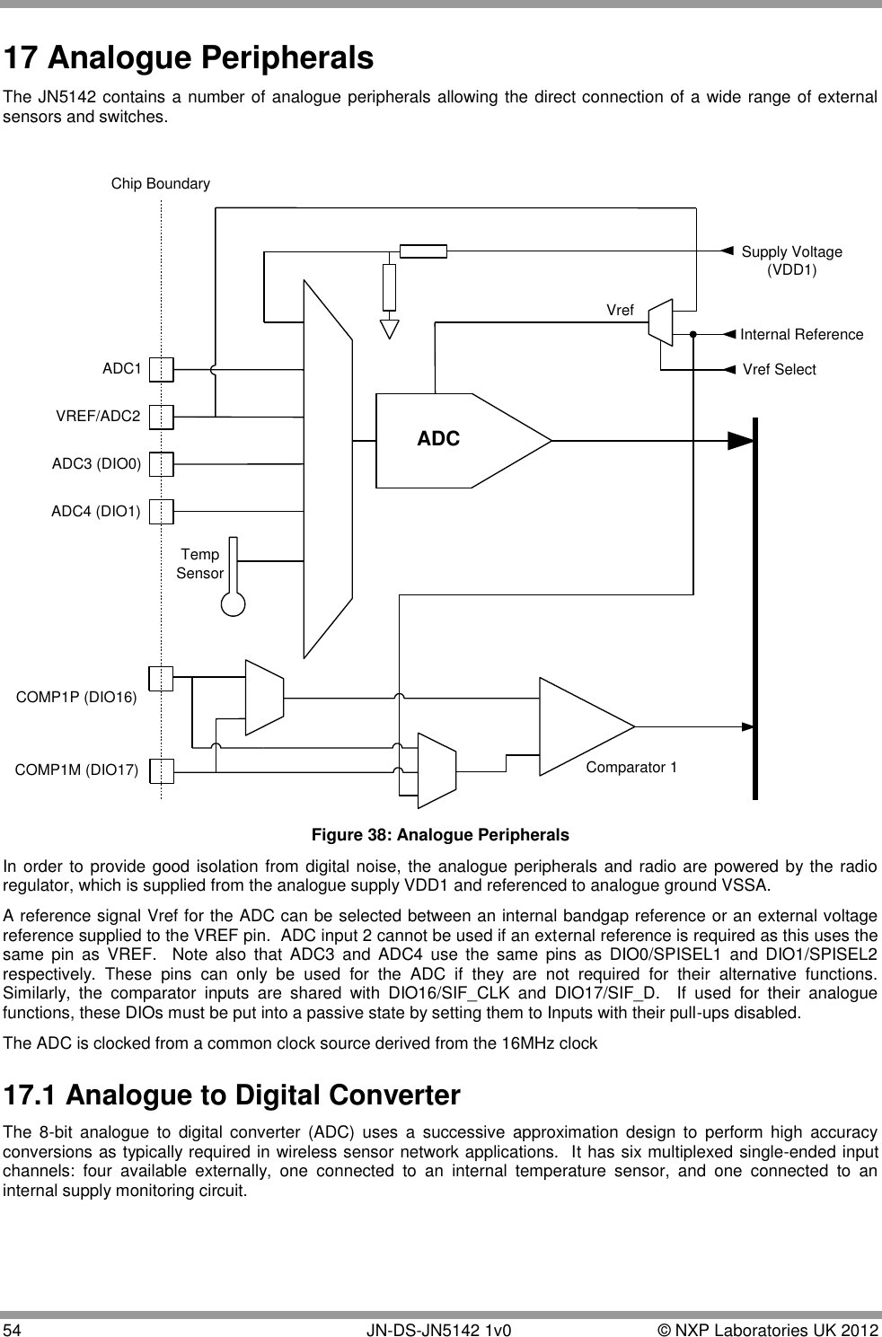
![14 JN-DS-JN5142 1v0 © NXP Laboratories UK 2012 OVDD2VSSPuRPUOEDIO[x] PinRESDADC orCOMP1 InputIIERPROTVSS Figure 4: DIO Pin Equivalent Schematic In reset, the digital peripherals are all off and the DIO pins are set as high-impedance inputs. During sleep and deep sleep, the DIO pins retain both their input/output state and output level that was set as sleep commences. If the DIO pins were enabled as inputs and the interrupts were enabled then these pins may be used to wake up the JN5142 from sleep.](https://usermanual.wiki/NXP-Laboratories-UK/JN5142M0.Datasheet/User-Guide-1655318-Page-14.png)

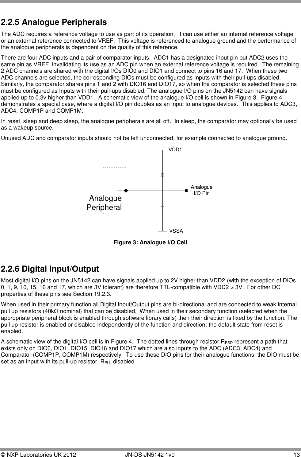
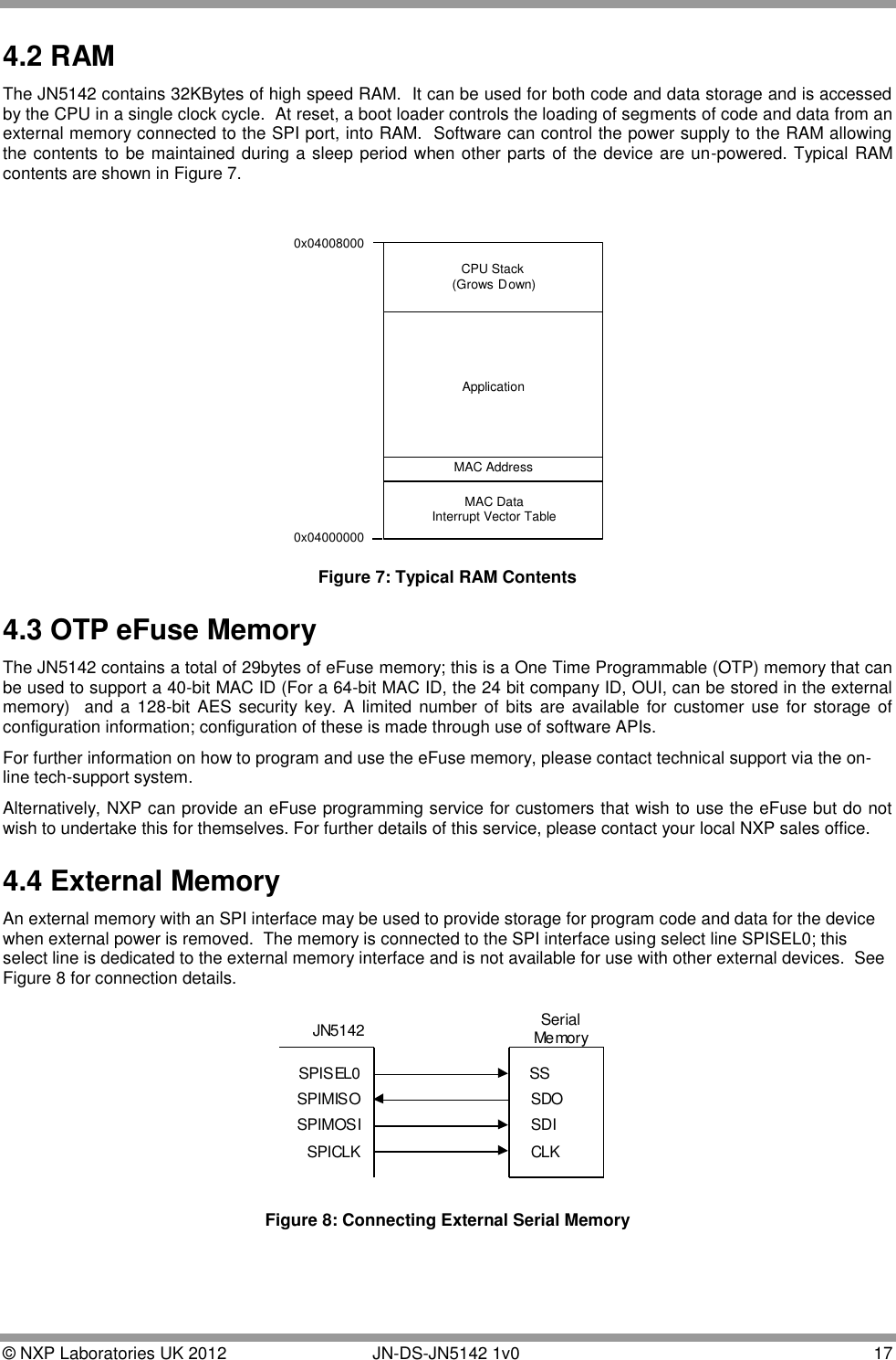
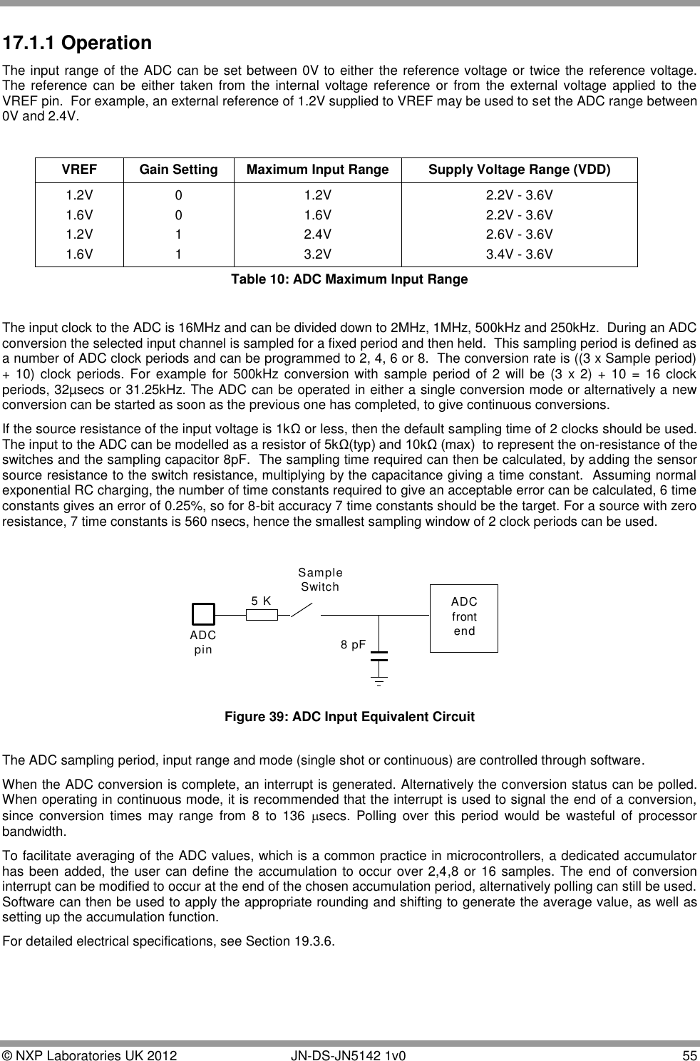
![16 JN-DS-JN5142 1v0 © NXP Laboratories UK 2012 4 Memory Organisation This section describes the different memories found within the JN5142. The device contains ROM, RAM, OTP eFuse memory, the wireless transceiver and peripherals all within the same linear address space. 0x000000000x00020000RAM(32KB)0xF00000000xFFFFFFFFUnpopulatedROM(128KB)0xF0008000RAM Echo0x04000000Peripherals0x02000000 Figure 5: JN5142 Memory Map 4.1 ROM The ROM is 128k bytes in size, and can be accessed by the processor in a single CPU clock cycle. The ROM contents include bootloader to allow external Flash memory contents to be bootloaded into RAM at runtime, a default interrupt vector table, an interrupt manager, IEEE802.15.4 MAC and APIs for interfacing on-chip peripherals. The operation of the boot loader is described in detail in Application Note [9]. The interrupt manager routes interrupt calls to the application‟s soft interrupt vector table contained within RAM. Section 7 contains further information regarding the handling of interrupts. ROM contents are shown in Figure 6. Interrupt VectorsInterrupt ManagerBoot LoaderIEEE802.15.4 Stack0x000000000x00020000APIsSpareNetwork Stack Figure 6: Typical ROM Contents](https://usermanual.wiki/NXP-Laboratories-UK/JN5142M0.Datasheet/User-Guide-1655318-Page-16.png)
![18 JN-DS-JN5142 1v0 © NXP Laboratories UK 2012 At reset, the contents of this memory are copied into RAM by the software boot loader. The Flash and EEPROM memory devices that are supported as standard through the JN5142 bootloader are given in Table 1. NXP recommends that where possible one of these devices should be selected. Manufacturer Part Number Size Type Micron (Numonyx) M25P10A M25P05A 1 Mbit 512 kbit Flash Flash Winbond W25X20B W25X10B 2 Mbit 1 Mbit Flash Flash Microchip 25AA080 25AA160 25AA320 8 kbit 16 kbit 32 kbit EEPROM EEPROM EEPROM Table 1: Supported Flash and EEPROM Memories Applications wishing to use an alternate Flash memory device should refer to Application Note [2]. This application note provides guidance on developing an interface to an alternate device. 4.4.1 External Memory Encryption The contents of the external serial memory may be encrypted. The AES security processor combined with a user programmable 128-bit encryption key is used to encrypt the contents of the external memory. The encryption key is stored in eFuse. When bootloading program code from external serial memory, the JN5142 automatically accesses the encryption key to execute the decryption process. User program code does not need to handle any of the decryption process; it is transparent. With encryption enabled, the time taken to boot code from external flash is increased. 4.5 Peripherals All peripherals have their registers mapped into the memory space. Access to these registers requires 3 clock cycles. Applications have access to the peripherals through the software libraries that present a high-level view of the peripheral‟s functions through a series of dedicated software routines. These routines provide both a tested method for using the peripherals and allow bug-free application code to be developed more rapidly. For details, see [5]. 4.6 Unused Memory Addresses Any attempt to access an unpopulated memory area will result in a bus error exception (interrupt) being generated.](https://usermanual.wiki/NXP-Laboratories-UK/JN5142M0.Datasheet/User-Guide-1655318-Page-18.png)

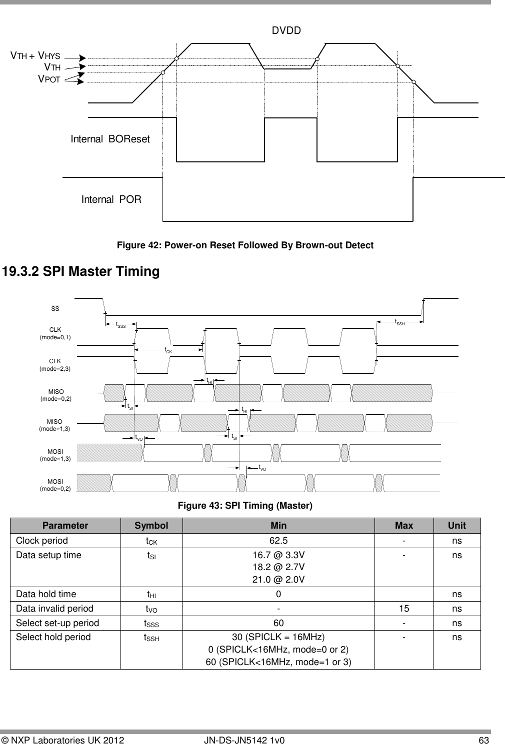
![22 JN-DS-JN5142 1v0 © NXP Laboratories UK 2012 6 Reset A system reset initialises the device to a pre-defined state and forces the CPU to start program execution from the reset vector. The reset process that the JN5142 goes through is as follows. When power is first applied or when the external reset is released, the High-Speed RC oscillator and 32MHz crystal oscillator are activated. After a short wait period (13sec approx) while the High-Speed RC starts up, and so long as the supply voltage satisfies the default Supply Voltage Monitor (SVM) threshold (2.0V+0.045V hysteresis), the internal 1.8V regulators are turned on to power the processor and peripheral logic. This is followed by a further wait (again 13sec approx) before the eFuse SVM threshold is read and applied. After a brief pause (approx 2.5sec) the SVM is checked again with the new threshold and if successful, the internal reset is removed from the CPU and peripheral logic and the CPU starts to run code beginning at the reset vector, consisting of initialisation code and the resident boot loader. [9] Section 19.3.1 provides detailed electrical data and timing. The JN5142 has five sources of reset: Internal Power-on / Brown-out Reset (BOR) External Reset Software Reset Watchdog timer Supply Voltage detect Note: When the device exits a reset condition, device operating parameters (voltage, frequency, temperature, etc.) must be met to ensure operation. If these conditions are not met, then the device must be held in reset until the operating conditions are met. (See Section 19.3) 6.1 Internal Power-On / Brown-out Reset (BOR) For the majority of applications the internal power-on reset is capable of generating the required reset signal. When power is applied to the device, the power-on reset circuit monitors the rise of the VDD supply. When the VDD reaches the specified threshold, the reset signal is generated. This signal is held internally until the power supply and oscillator stabilisation time has elapsed, when the internal reset signal is then removed and the CPU is allowed to run. The BOR circuit has the ability to reject spikes on the VDD rail to avoid false triggering of the reset module. Typically for a negative going square pulse of duration 1uS, the voltage must fall to 1.2v before a reset is generated. Similarly for a triangular wave pulse of 10us width, the voltage must fall to 1.3v before causing a reset. The exact characteristics are complex and these are only examples. RESETN PinInternal RESETVDD Figure 11: Internal Power-on Reset When the supply drops below the power on reset „falling‟ threshold, it will re-trigger the reset. If necessary, use of the external reset circuit show in Figure 12 is suggested.](https://usermanual.wiki/NXP-Laboratories-UK/JN5142M0.Datasheet/User-Guide-1655318-Page-22.png)

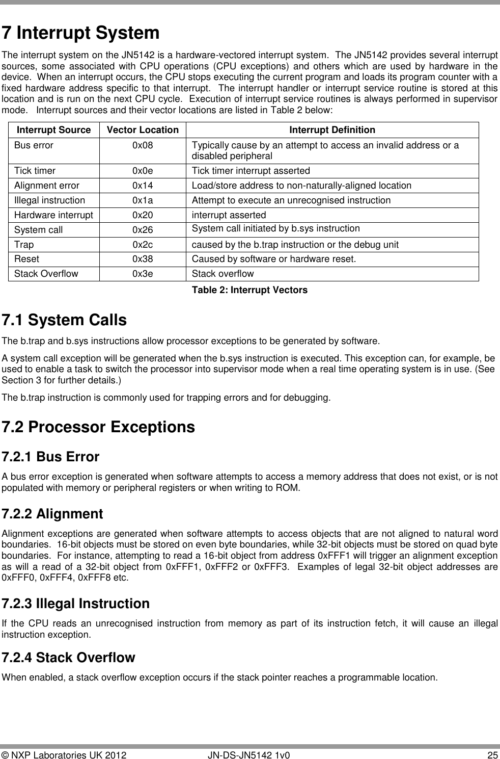
![26 JN-DS-JN5142 1v0 © NXP Laboratories UK 2012 7.3 Hardware Interrupts Hardware interrupts generated from the transceiver, analogue or digital peripherals and DIO pins are individually masked using the Programmable Interrupt Controller (PIC). Management of interrupts is provided in the peripherals library [5]. For details of the interrupts generated from each peripheral see the respective section in this datasheet. Interrupts can be used to wake the JN5142 from sleep. The peripherals, baseband controller, security coprocessor and PIC are powered down during sleep but the DIO interrupts and optionally the pulse counters, wake-up timers and analogue comparator interrupts remain powered to bring the JN5142 out of sleep. Prioritised external interrupt handling (i.e., interrupts from hardware peripherals) is provided to enable an application to control an events priority to provide for deterministic program execution. The priority Interrupt controller provides 15 levels of prioritised interrupts. The priority level of all interrupts can be set, with value 0 being used to indicate that the source can never produce an external interrupt, 1 for the lowest priority source(s) and 15 for the highest priority source(s). Note that multiple interrupt sources can be assigned the same priority level if desired. If while processing an interrupt, a new event occurs at the same or lower priority level, a new external interrupt will not be triggered. However, if a new higher priority event occurs, the external interrupt will again be asserted, interrupting the current interrupt service routine. Once the interrupt service routine is complete, lower priority events can be serviced.](https://usermanual.wiki/NXP-Laboratories-UK/JN5142M0.Datasheet/User-Guide-1655318-Page-26.png)

![© NXP Laboratories UK 2012 JN-DS-JN5142 1v0 29 Antenna A Antenna BABCOMSELSELBADO (DIO[12])ADE (DIO[13])Device RF PortRF Switch: Single-Pole, Double-Throw (SPDT) Figure 16: Simple Antenna Diversity Implementation using External RF Switch ADO (DIO[12])TX ActiveRX ActiveADE (DIO[13])1st TX-RX Cycle 2nd TX-RX Cycle (1st Retry) Figure 17: Antenna Diversity ADO Signal for TX with Acknowledgement If two DIO pins cannot be spared, DIO13 can be configured to be a normal DIO pin, and the inverse of ADO generated with an inverter on the PCB.](https://usermanual.wiki/NXP-Laboratories-UK/JN5142M0.Datasheet/User-Guide-1655318-Page-29.png)
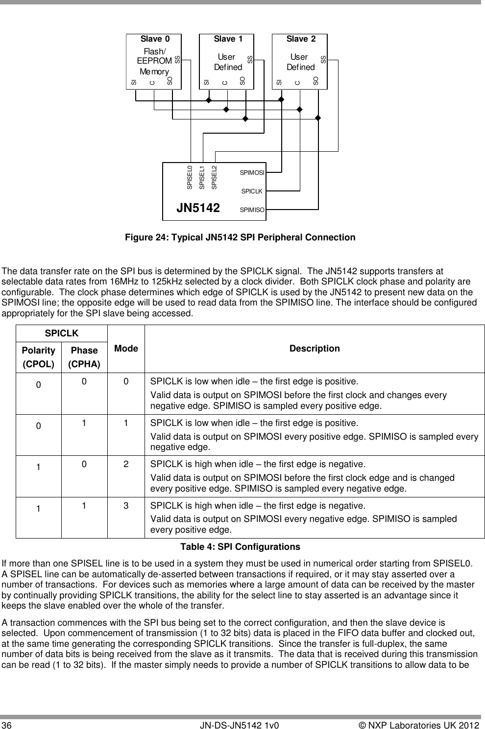
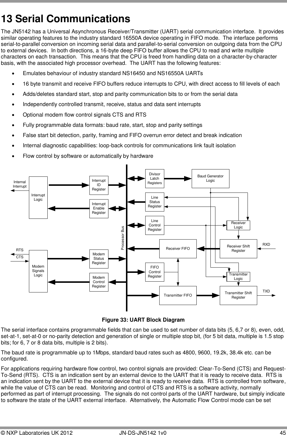
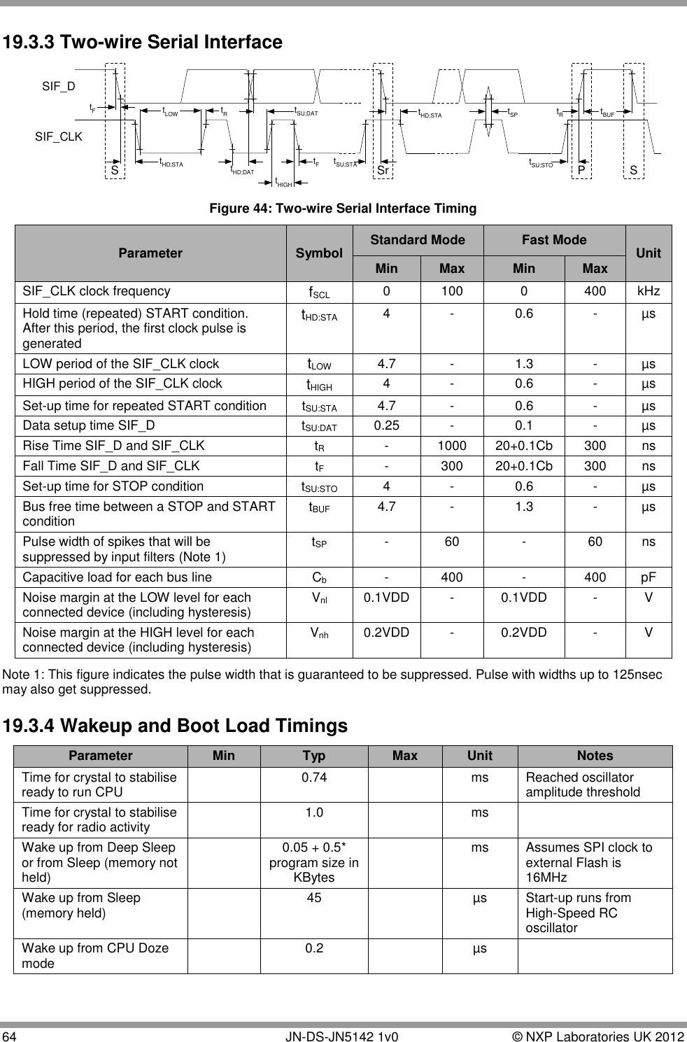
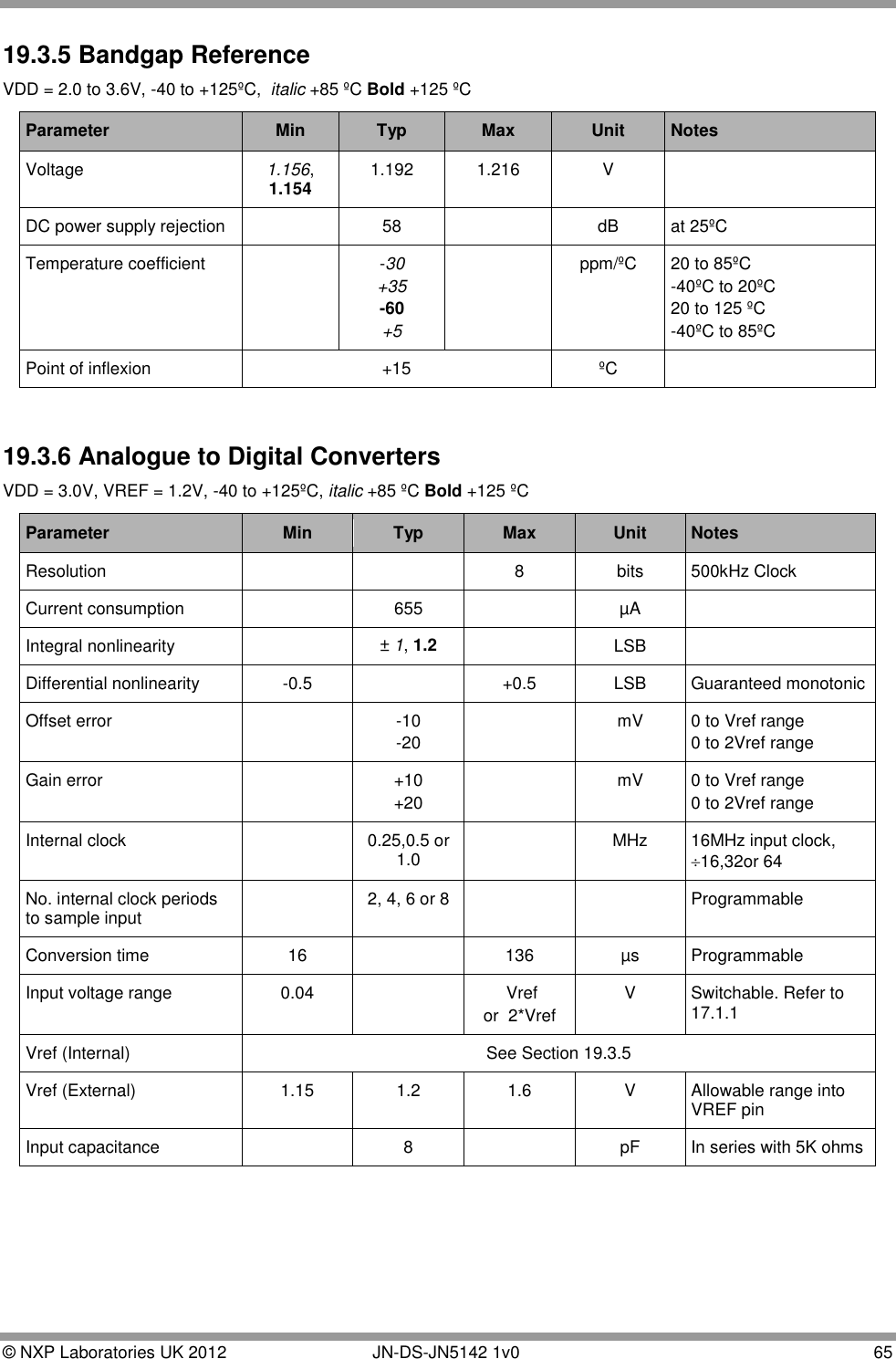
![© NXP Laboratories UK 2012 JN-DS-JN5142 1v0 35 10 Serial Peripheral Interface The Serial Peripheral Interface (SPI) allows high-speed synchronous data transfer between the JN5142 and peripheral devices. The JN5142 operates as a master on the SPI bus and all other devices connected to the SPI are expected to be slave devices under the control of the JN5142 CPU. The SPI includes the following features: Full-duplex, three-wire synchronous data transfer Programmable bit rates (up to 16Mbit/s) Programmable transaction size up to 32-bits Standard SPI modes 0,1,2 and 3 Manual or Automatic slave select generation (up to 3 slaves) Maskable transaction complete interrupt LSB First or MSB First Data Transfer Supports delayed read edges ClockDividerSPI BusCycleControllerData BufferDIVClock EdgeSelectDataCHAR_LENLSBSPIMISOSPIMOSISPICLKSelectLatchSPISEL [2..0]16 MHz Figure 23: SPI Block Diagram The SPI bus employs a simple shift register data transfer scheme. Data is clocked out of and into the active devices in a first-in, first-out fashion allowing SPI devices to transmit and receive data simultaneously. There are three dedicated pins SPICLK, SPIMOSI, SPIMISO that are shared across all devices on the bus. Master-Out-Slave-In or Master-In-Slave-Out data transfer is relative to the clock signal SPICLK generated by the JN5142. The JN5142 provides three slave selects, SPISEL0 to SPISEL2 to allow three SPI peripherals on the bus. SPISEL0 is a dedicated pin; this is generally connected to a serial Flash/EEPROM memory holding application code that is downloaded to internal RAM via software from reset. SPISEL1 is accessed, depending upon the configuration, on DIO0 or DIO14. SPISEL2 is accessed on DIO1 or DIO15. This is enabled under software control. The following table details which DIO are used for the SPISEL signals depending upon the configuration. Signal DIO Assignment Standard pins Alternative pins SPISEL1 16 38 SPISEL2 17 40 Table 3: SPISEL IO The interface can transfer from 1 to 32-bits without software intervention and can keep the slave select lines asserted between transfers when required, to enable longer transfers to be performed. When the device reset is active, the three outputs SPISEL, SPICLK and SPI_MOSI are tri-stated and SPI_MISO is set to be an input. The pull-up resistors associated with all four pins will be active at this time.](https://usermanual.wiki/NXP-Laboratories-UK/JN5142M0.Datasheet/User-Guide-1655318-Page-35.png)
![48 JN-DS-JN5142 1v0 © NXP Laboratories UK 2012 14 JTAG Debug Interface The JN5142 includes an IEEE1149.1 compliant JTAG port for the sole purpose of software code debug with the Software Development Kit. The JTAG interface is disabled by default and is enabled under software control. Therefore, debugging is only possible if enabled by the application. Once enabled, the application executes as normal until the external debugger controller initiates debug activity. The Debugger supports breakpoints and watchpoints based on four comparisons between any of program counter, load/store effective address and load/store data. There is the ability to chain the comparisons together. There is also the ability, under debugger control to perform the following commands: go, stop, reset, step over/into/out/next, run to cursor and breakpoints. In addition, under control of the debugger, it is possible to: Read and write registers on the wishbone bus Read ROM and RAM, and write to RAM Read and write CPU internal registers The Debugger interface is accessed, depending upon the configuration, through the standard or alternative pins used for UART0. This is enabled under software control and is dealt with in [4]. The following table details which DIO are used for the JTAG interface depending upon the configuration. Signal DIO Assignment Standard pins Alternative pins clock (TCK) 26 36 control (TMS) 27 37 data out (TDO) 28 38 data in (TDI) 29 40 Table 7: Hardware Debugger IO If doze mode is active when debugging is started, the processor will be woken and then respond to debugger commands. It is not possible to wake the device from sleep using the debug interface and debugging is not available while the device is sleeping. When using the debug interface, program execution is halted, and control of the CPU is handed to the debugger. The watchdog, tick timer and the timers described in Section 11 are stalled while the debugger is in control of the CPU. When control is handed from the CPU to the debugger or back a small number of CPU clock cycles are taken flushing or reloading the CPU pipeline. Because of this, when a program is halted by the debugger and then restarted again, a small number of tick timer cycles will elapse. It is possible to prevent all hardware debugging by blowing the relevant Efuse bit. For further information on how to program the eFuse, please contact technical support via the on-line tech-support system. The JTAG interface does not support boundary scan testing. It is recommended that the JN5142 is not connected as part of the board scan chain.](https://usermanual.wiki/NXP-Laboratories-UK/JN5142M0.Datasheet/User-Guide-1655318-Page-48.png)


![70 JN-DS-JN5142 1v0 © NXP Laboratories UK 2012 Radio Parameters: 2.0-3.6V, +25ºC Parameter Min Typical Max Unit Notes Receiver Characteristics Receive sensitivity -92 -95 dBm Nominal for 1% PER, as per 802.15.4 Section 6.5.3.3 Maximum input signal +10 dBm For 1% PER, measured as sensitivity Adjacent channel rejection (-1/+1 ch) [CW Interferer] 19/34 [27/49] dBc For 1% PER, with wanted signal 3dB, above sensitivity. (Note1,2) (modulated interferer) Alternate channel rejection (-2/+2 ch) [CW Interferer] 40/45 [54/54] dBc For 1% PER, with wanted signal 3dB, above sensitivity. (Note1,2) (modulated interferer) Other in band rejection 2.4 to 2.4835 GHz, excluding adj channels 48 dBc For 1% PER with wanted signal 3dB above sensitivity. (Note1) Out of band rejection 52 dBc For 1% PER with wanted signal 3dB above sensitivity. All frequencies except wanted/2 which is 8dB lower. (Note1) Spurious emissions (RX) -61 <-70 -58 dBm Measured conducted into 50ohms 30MHz to 1GHz 1GHz to 12GHz Intermodulation protection 40 dB For 1% PER at with wanted signal 3dB above sensitivity. Modulated Interferers at 2 & 4 channel separation (Note1) RSSI linearity -4 +4 dB -95 to -10dBm. Available through Hardware API Transmitter Characteristics Transmit power +0.5 +2.5 dBm Output power control range -35 dB In three 12dB steps (Note3) Spurious emissions (TX) -40 <-70 <-70 dBm Measured conducted into 50ohms 30MHz to 1GHz, 1GHz to12.5GHz, The following exceptions apply 1.8 to 1.9GHz & 5.15 to 5.3GHz EVM [Offset] 10 [2.0] 15 % At maximum output power Transmit Power Spectral Density -38 -20 dBc At greater than 3.5MHz offset, as per 802.15.4, Section 6.5.3.1](https://usermanual.wiki/NXP-Laboratories-UK/JN5142M0.Datasheet/User-Guide-1655318-Page-70.png)
![© NXP Laboratories UK 2012 JN-DS-JN5142 1v0 71 Radio Parameters: 2.0-3.6V, -40ºC Parameter Min Typical Max Unit Notes Receiver Characteristics Receive sensitivity -93.5 -96.5 dBm Nominal for 1% PER, as per 802.15.4 Section 6.5.3.3 Maximum input signal +10 dBm For 1% PER, measured as sensitivity Adjacent channel rejection (-1/+1 ch) [CW Interferer] 19/34 [TBC] dBc For 1% PER, with wanted signal 3dB, above sensitivity. (Note1,2) (modulated interferer) Alternate channel rejection (-2/+2 ch) [CW Interferer] 40/45 [TBC] dBc For 1% PER, with wanted signal 3dB, above sensitivity. (Note1,2) (modulated interferer) Other in band rejection 2.4 to 2.4835 GHz, excluding adj channels 47 dBc For 1% PER with wanted signal 3dB above sensitivity. (Note1) Out of band rejection 49 dBc For 1% PER with wanted signal 3dB above sensitivity. All frequencies except wanted/2 which is 8dB lower. (Note1) Spurious emissions (RX) -60 <-70 -57 dBm Measured conducted into 50ohms 30MHz to 1GHz 1GHz to 12GHz Intermodulation protection 39 dB For 1% PER at with wanted signal 3dB above sensitivity. Modulated Interferers at 2 & 4 channel separation (Note1) RSSI linearity -4 +4 dB -95 to -10dBm. Available through Hardware API Transmitter Characteristics Transmit power +0.75 +2.75 dBm Output power control range -35 dB In three 12dB steps (Note3) Spurious emissions (TX) -40 <-70 <-70 dBm Measured conducted into 50ohms 30MHz to 1GHz, 1GHz to12.5GHz, The following exceptions apply 1.8 to 1.9GHz & 5.15 to 5.3GHz EVM [Offset] 9 [2.0] 15 % At maximum output power Transmit Power Spectral Density -38 -20 dBc At greater than 3.5MHz offset, as per 802.15.4, Section 6.5.3.1](https://usermanual.wiki/NXP-Laboratories-UK/JN5142M0.Datasheet/User-Guide-1655318-Page-71.png)
![72 JN-DS-JN5142 1v0 © NXP Laboratories UK 2012 Radio Parameters: 2.0-3.6V, +85ºC Parameter Min Typical Max Unit Notes Receiver Characteristics Receive sensitivity -90 -93 dBm Nominal for 1% PER, as per 802.15.4 Section 6.5.3.3 Maximum input signal +5 dBm For 1% PER, measured as sensitivity Adjacent channel rejection (-1/+1 ch) [CW Interferer] 19/34 [TBC] dBc For 1% PER, with wanted signal 3dB, above sensitivity. (Note1,2) (modulated interferer) Alternate channel rejection (-2/+2 ch) [CW Interferer] 40/45 [TBC] dBc For 1% PER, with wanted signal 3dB, above sensitivity. (Note1,2) (modulated interferer) Other in band rejection 2.4 to 2.4835 GHz, excluding adj channels 49 dBc For 1% PER with wanted signal 3dB above sensitivity. (Note1) Out of band rejection 53 dBc For 1% PER with wanted signal 3dB above sensitivity. All frequencies except wanted/2 which is 8dB lower. (Note1) Spurious emissions (RX) -62 <-70 -59 dBm Measured conducted into 50ohms 30MHz to 1GHz 1GHz to 12GHz Intermodulation protection 41 dB For 1% PER at with wanted signal 3dB above sensitivity. Modulated Interferers at 2 & 4 channel separation (Note1) RSSI linearity -4 +4 dB -95 to -10dBm. Available through Hardware API Transmitter Characteristics Transmit power -0.2 +1.8 dBm Output power control range -35 dB In three 12dB steps (Note3) Spurious emissions (TX) -38 <-70 <-70 dBm Measured conducted into 50ohms 30MHz to 1GHz, 1GHz to12.5GHz, The following exceptions apply 1.8 to 1.9GHz & 5.15 to 5.3GHz EVM [Offset] 10 [2.0] 15 % At maximum output power Transmit Power Spectral Density -38 -20 dBc At greater than 3.5MHz offset, as per 802.15.4, Section 6.5.3.1](https://usermanual.wiki/NXP-Laboratories-UK/JN5142M0.Datasheet/User-Guide-1655318-Page-72.png)
![© NXP Laboratories UK 2012 JN-DS-JN5142 1v0 73 Radio Parameters: 2.0-3.6V, +125ºC Parameter Min Typical Max Unit Notes Receiver Characteristics Receive sensitivity -88 -91 dBm Nominal for 1% PER, as per 802.15.4 Section 6.5.3.3 Maximum input signal 0 dBm For 1% PER, measured as sensitivity Adjacent channel rejection (-1/+1 ch) [CW Interferer] 20/34 [TBC] dBc For 1% PER, with wanted signal 3dB, above sensitivity. (Note1,2) (modulated interferer) Alternate channel rejection (-2/+2 ch) [CW Interferer] 40/45 [TBC] dBc For 1% PER, with wanted signal 3dB, above sensitivity. (Note1,2) (modulated interferer) Other in band rejection 2.4 to 2.4835 GHz, excluding adj channels 49 dBc For 1% PER with wanted signal 3dB above sensitivity. (Note1) Out of band rejection 53 dBc For 1% PER with wanted signal 3dB above sensitivity. All frequencies except wanted/2 which is 8dB lower. (Note1) Spurious emissions (RX) -64 <-70 -61 dBm Measured conducted into 50ohms 30MHz to 1GHz 1GHz to 12GHz Intermodulation protection 41 dB For 1% PER at with wanted signal 3dB above sensitivity. Modulated Interferers at 2 & 4 channel separation (Note1) RSSI linearity -4 +4 dB -95 to -10dBm. Available through Hardware API Transmitter Characteristics Transmit power -0.8 +1.2 dBm Output power control range -35 dB In three 12dB steps (Note3) Spurious emissions (TX) -37 <-70 <-70 dBm Measured conducted into 50ohms 30MHz to 1GHz, 1GHz to12.5GHz, The following exceptions apply 1.8 to 1.9GHz & 5.15 to 5.3GHz EVM [Offset] 10 [3.0] 15 % At maximum output power Transmit Power Spectral Density -38 -20 dBc At greater than 3.5MHz offset, as per 802.15.4, Section 6.5.3.1](https://usermanual.wiki/NXP-Laboratories-UK/JN5142M0.Datasheet/User-Guide-1655318-Page-73.png)


![84 JN-DS-JN5142 1v0 © NXP Laboratories UK 2012 B.1.3 Crystal ESR and Required Transconductance The resistor in the crystal equivalent circuit represents the energy lost. To maintain oscillation, power must be supplied by the amplifier, but how much? Firstly, the Pi connected capacitors C1 and C2 with CS from the crystal, apply an impedance transformation to Rm, when viewed from the amplifier. This new value is given by: 2ˆLLSmm CCCRR The amplifier is a transconductance amplifier, which takes a voltage and produces an output current. The amplifier together with the capacitors C1 and C2, form a circuit, which provides a negative resistance, when viewed from the crystal. The value of which is given by: 221TTmNEG CCgR Where mgis the transconductance is the frequency in rad/s Derivations of these formulas can be easily found in textbooks. In order to give quick and reliable oscillator start-up, a common rule of thumb is to set the amplifier negative resistance to be a minimum of 4 times the effective crystal resistance. This gives 221 TTmCCg 24LLSmCCCR This can be used to give an equation for the required transconductance. 21221212])([4TTTTTTSmmCC CCCCCRg Example: Using typical 32MHz crystal parameters of mR=40, SC=1pF and 1TC=2TC=18pF ( for a load capacitance of 9pF), the equation above gives the required transconductance (mg) as 2.59mA/V. The JN5142 has a typical value for transconductance of 4.3mA/V The example and equation illustrate the trade-off that exists between the load capacitance and crystal ESR. For example, a crystal with a higher load capacitance can be used, but the value of max. ESR that can be tolerated is reduced. Also note, that the circuit sensitivity to external capacitance [ C1 , C2 ] is a square law. Meeting the criteria for start-up is only one aspect of the way these parameters affect performance, they also affect the time taken during start-up to reach a given, (or full), amplitude. Unfortunately, there is no simple mathematical model for this, but the trend is the same. Therefore, both a larger load capacitance and larger crystal ESR will give a longer start-up time, which has the disadvantages of reduced battery life and increased latency.](https://usermanual.wiki/NXP-Laboratories-UK/JN5142M0.Datasheet/User-Guide-1655318-Page-84.png)
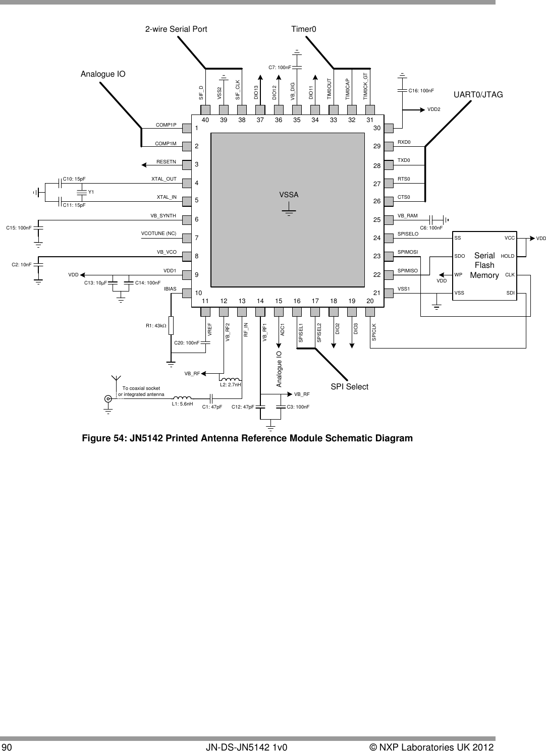
![© NXP Laboratories UK 2012 JN-DS-JN5142 1v0 89 B.4 JN5142 Module Reference Designs For customers wishing to integrate the JN5142 device directly into their system, NXP provide a range of Module Reference Designs, covering standard and high-power modules fitted with different Antennae To ensure the correct performance, it is strongly recommended that where possible the design details provided by the reference designs, are used in their exact form for all end designs, this includes component values, pad dimensions, track layouts etc. In order to minimise all risks, it is recommended that the entire layout of the appropriate reference module, if possible, be replicated in the end design. For full details, see [6]. Please contact technical support via the on-line tech-support system. (www.jennic.com/support) B.4.1 Schematic Diagram A schematic diagram of the JN5142 PCB antenna reference module is shown in 140 39 38 37 36 35 34 33 32 31VSSA23456789103029282726252423222120191817161514131211COMP1P COMP1M RESETN XTAL_OUTXTAL_IN VB_SYNTH VCOTUNE (NC) VB_VCOVDD1IBIAS VREFVB_RF2 RF_INVB_RFADC1SPISEL1SPISEL2DIO2DIO3SPICLK VSS1 SPIMISO SPIMOSI SPISELO VB_RAM CTS0 RTS0 TXD0 RXD0 VDD2 SIF_D VSS2 SIF_CLK DIO13 DIO12 VB_DIG DIO11 TIM0OUT TIM0CAP TIM0CK_GT C7: 100nF2-wire Serial Port Timer0C16: 100nF UART0/JTAGC6: 100nFSerialFlashMemoryVDDSDOWPVSSSS VCCHOLDCLKSDISPI SelectAnalogue IOC12: 47pF C3: 100nFC1: 47pFL1: 5.6nHL2: 2.7nHVB_RFR1: 43kTo coaxial socketor integrated antennaC20: 100nFC14: 100nFC13: 10µFVDDC2: 10nF C15: 100nFC10: 15pFC11: 15pFY1Analogue IOVDDVB_RF1Figure 54. Details of component values and PCB layout constraints can be found in Table 13.](https://usermanual.wiki/NXP-Laboratories-UK/JN5142M0.Datasheet/User-Guide-1655318-Page-89.png)

![92 JN-DS-JN5142 1v0 © NXP Laboratories UK 2012 B.4.2 PCB Design and Reflow Profile PCB and land pattern designs are key to the reliability of any electronic circuit design. The Institute for Interconnecting and Packaging Electronic Circuits (IPC) defines a number of standards for electronic devices. One of these is the "Surface Mount Design and Land Pattern Standard" IPC-SM-782 [3], commonly referred to as “IPC782". This specification defines the physical packaging characteristics and land patterns for a range of surface mounted devices. IPC782 is also a useful reference document for general surface mount design techniques, containing sections on design requirements, reliability and testability. NXP strongly recommends that this be referred to when designing the PCB. NXP also provide application note AN10366, “HVQFN application information” [7] which describes the reflow soldering process. The suggested reflow profile, from that application note, is shown in Figure 55. The specific paste manufacturers guidelines on peak flow temperature, soak times, time above liquidus and ramp rates should also be referenced. Figure 55: Recommended Reflow Profile for Lead-free Solder Paste (SNAgCu) or PPF Lead Frame B.4.3 Moisture Sensitivity Level (MSL) If there is moisture trapped inside a package, and the package is exposed to a reflow temperature profile, the moisture may turn into steam, which expands rapidly. This may cause damage to the inside of the package (delamination), and it may result in a cracked semiconductor package body (the popcorn effect). A package‟s MSL depends on the package characteristics and on the temperature it is exposed to during reflow soldering. This is explained in more detail in [8]. Depending on the damage after this test, an MSL of 1 (not sensitive to moisture) to 6 (very sensitive to moisture) is attached to the semiconductor package.](https://usermanual.wiki/NXP-Laboratories-UK/JN5142M0.Datasheet/User-Guide-1655318-Page-92.png)
![© NXP Laboratories UK 2012 JN-DS-JN5142 1v0 93 Related Documents [1] IEEE Std 802.15.4-2006 IEEE Standard for Information Technology – Part 15.4 Wireless Medium Access Control (MAC) and Physical Layer (PHY) Specifications for Low-Rate Wireless Personal Area Networks (LR-WPANs). [2] JN-AN-1038 Programming Flash devices not supported by the JN51xx ROM-based bootloader [3] IPC-SM-782 Surface Mount Design and Land Pattern Standard [4] JN-AN-1118 JN514x Application Debugging [5] JN-UG-3066 JN51xx Integrated Peripherals API Reference Manual [6] JN-RD-6032 Standard Module Reference Design [7] http://www.nxp.com/documents/mounting_and_soldering/HVQFN_mounting.pdf [8] http://www.nxp.com/documents/mounting_and_soldering/AN10365.pdf [9] JN-AN-1003 Boot Loader Operation RoHS Compliance JN5142 devices meet the requirements of Directive 2002/95/EC of the European Parliament and of the Council on the Restriction of Hazardous Substance (RoHS) and of the China RoHS (SJ/T11363 – 2006) requirements which came into force on 1st March 2007. Status Information The status of this Data Sheet is. Preliminary NXP Low Power RF products progress according to the following format: Advance The Data Sheet shows the specification of a product in planning or in development. The functionality and electrical performance specifications are target values of the design and may be used as a guide to the final specification. Integrated circuits are identified with an Rx suffix, for example JN5142R1. NXP reserves the right to make changes to the product specification at anytime without notice. Preliminary The Data Sheet shows the specification of a product that is commercially available, but is not yet fully qualified. The functionality of the product is final. The electrical performance specifications are target values and may used as a guide to the final specification. Integrated circuits are identified with an Rx suffix, for example JN5142R1. NXP reserves the right to make changes to the product specification at anytime without notice. Production This is the production Data Sheet for the product. All functional and electrical performance specifications, where included, including min and max values are derived from detailed product characterization. This Data Sheet supersedes all previous document versions. NXP reserves the right to make changes to the product specification at anytime.](https://usermanual.wiki/NXP-Laboratories-UK/JN5142M0.Datasheet/User-Guide-1655318-Page-93.png)