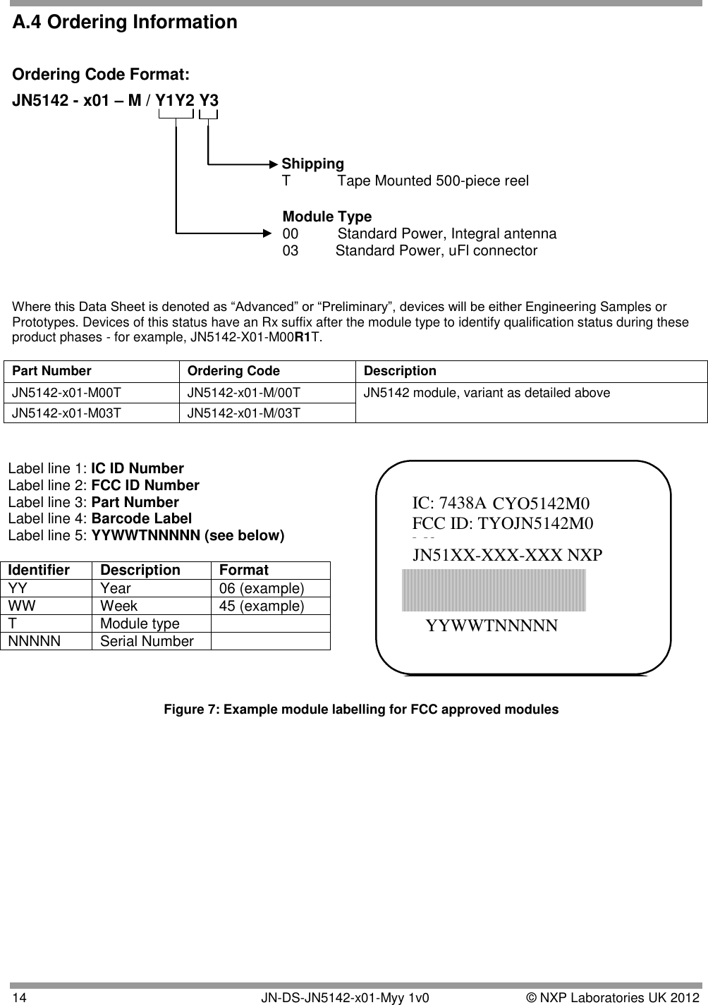
NXP Laboratories UK JN5142M0 JN5142-001-M00 IEEE802.15.4 Wireless Module User Manual JN DS JN5142 x01 Myy
NXP Laboratories UK Ltd JN5142-001-M00 IEEE802.15.4 Wireless Module JN DS JN5142 x01 Myy
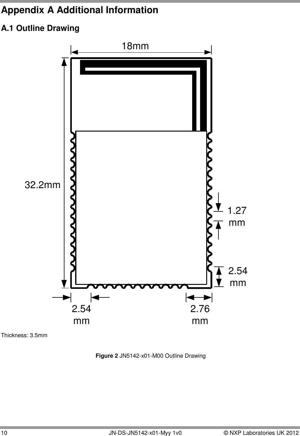
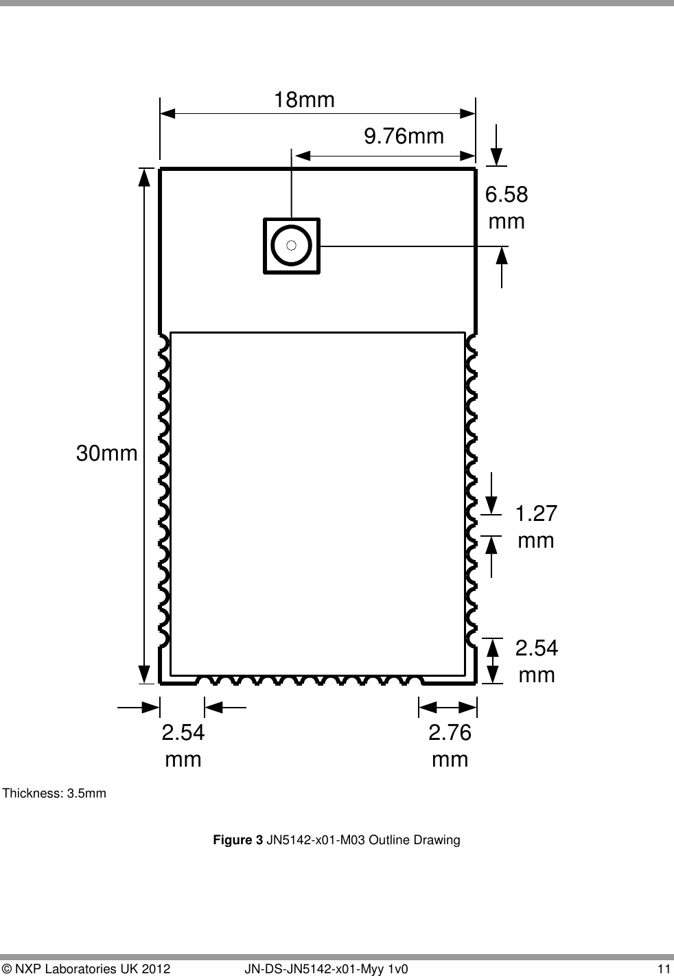
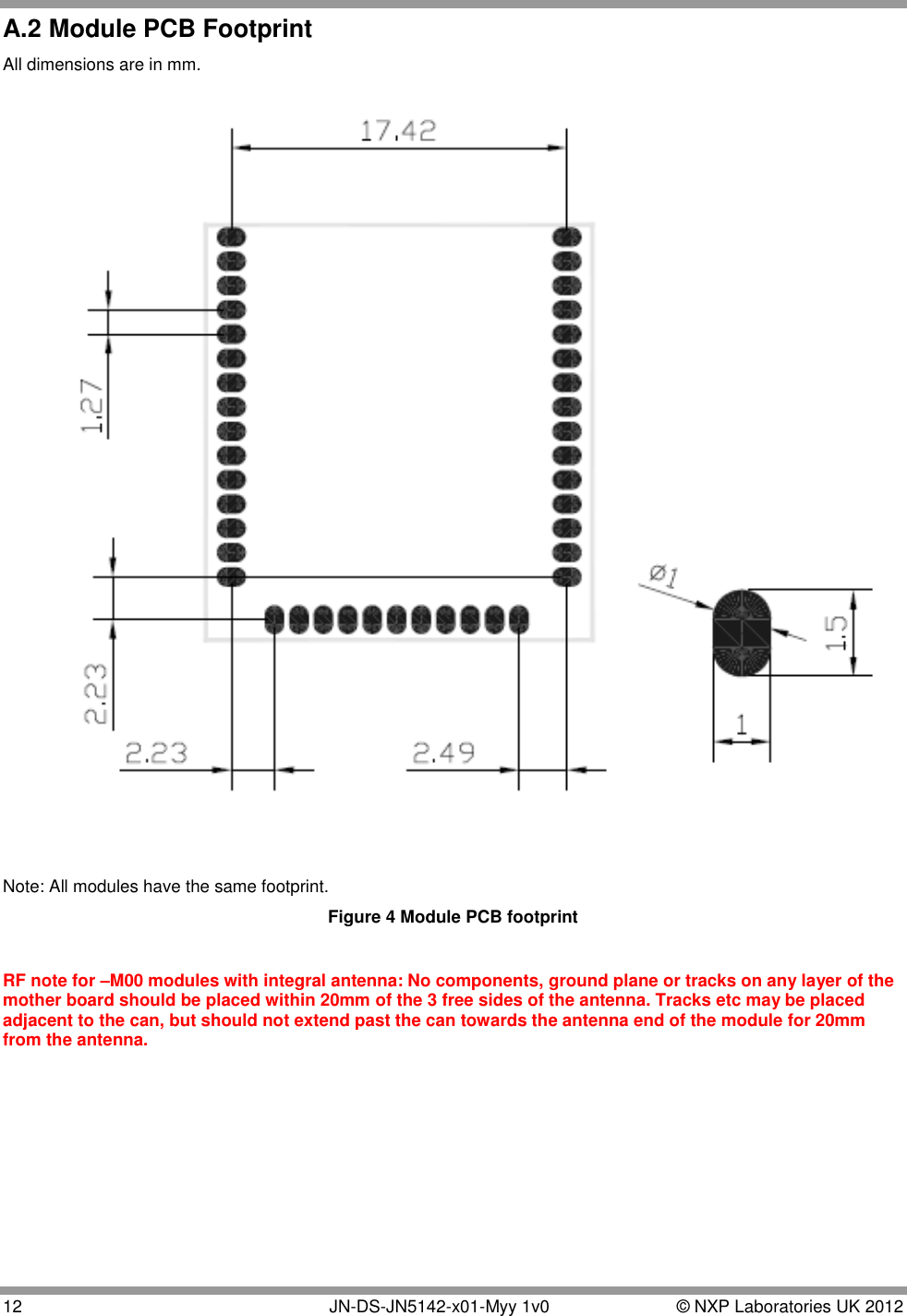
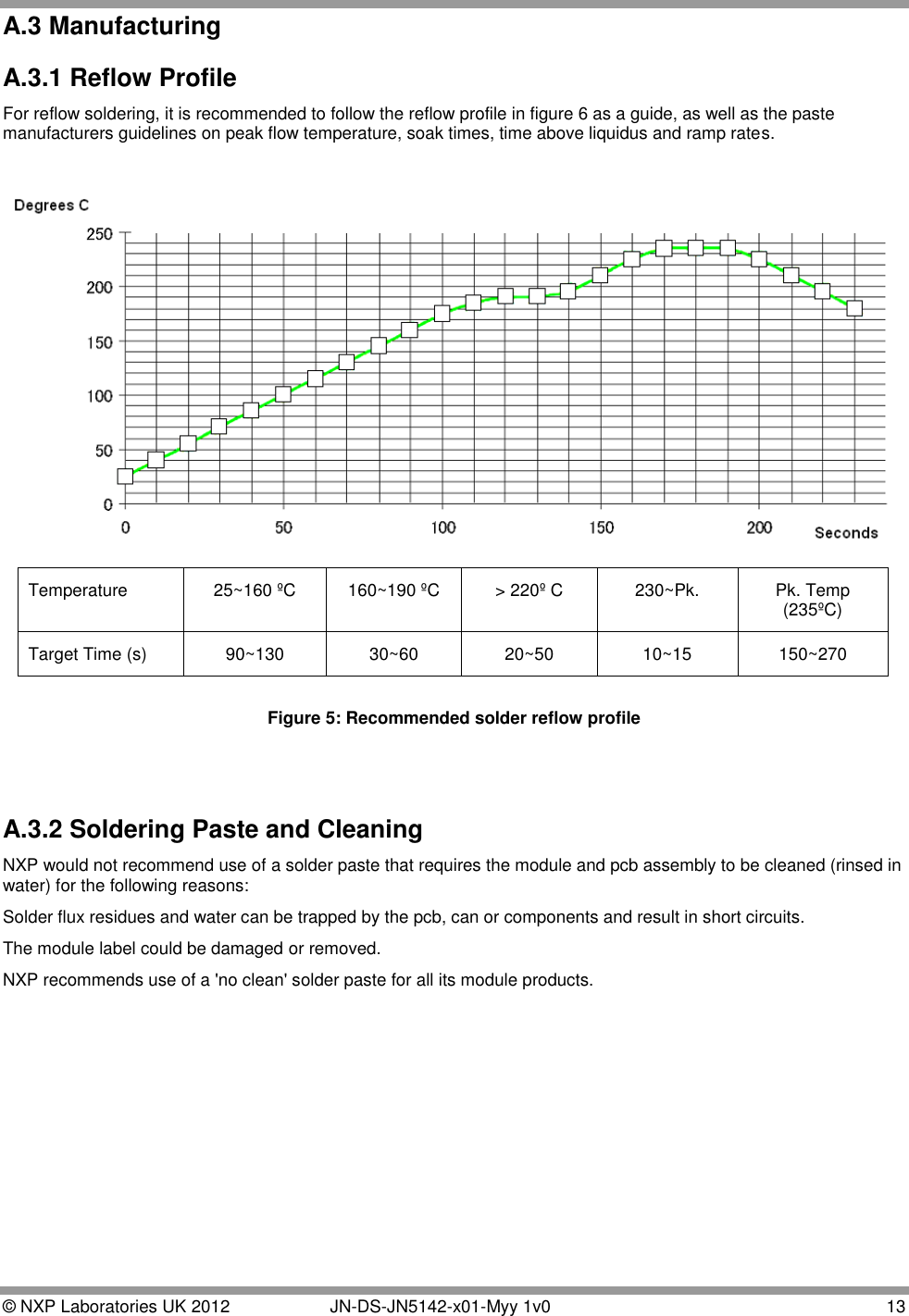
Contents
- 1. Datasheet
- 2. User Datasheet
- 3. Antenna Datasheet
User Datasheet
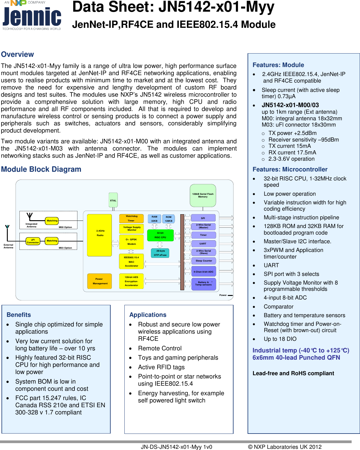
![© NXP Laboratories UK 2012 JN-DS-JN5142-x01-Myy 1v0 3 1. Introduction The JN5142-x01-Myy module family provides designers with a ready-made component that provides a fully integrated solution for applications using the IEEE802.15.4 standard in the 2.4 - 2.5GHz ISM frequency band [1], including RF4CE. A later version of the JN5142 will provide support for JenNet-IP “Smart Device” applications such as lighting. Applications that transfer data wirelessly tend to be more complex than wired ones. Wireless protocols make stringent demands on frequencies, data formats, timing of data transfers, security and other issues. Application development must consider the requirements of the wireless network in addition to the product functionality and user interfaces. To minimise this complexity, NXP provides a series of software libraries and interfaces that control the transceiver and peripherals of the JN5142. These libraries and interfaces remove the need for the developer to understand wireless protocols and greatly simplifies the programming complexities of power modes, interrupts and hardware functionality. In view of the above, it is not necessary to provide the register details of the JN5142 in the datasheet. The device includes a Wireless Transceiver, RISC CPU, on chip memory and an extensive range of peripherals. The modules integrate all of the RF components required, removing the need to perform expensive RF design and test. Products can be designed by simply connecting sensors and switches to the module IO pins. The modules use an NXP single chip IEEE802.15.4 Wireless Microcontroller, allowing designers to make use of the extensive chip development support material. Hence, this range of modules allows designers to bring wireless applications to market in the minimum time with significantly reduced development effort and cost. Two variants are available: JN5142-x01-M00 (standard module with integral antenna) and the JN5142-x01-M03 (standard module with uFL connector for use with external antennae). All modules have FCC modular approvals and are compliant with EU regulations. The variants available are described below. 1.1. Variants 1.2. Regulatory Approvals All module types have been tested against the requirements of European standard EN 300 328 v1.7.1 and a Notified Body statement of opinion for this standard is available on request. Additionally, all module types have received FCC “Modular Approvals”, in compliance with CFR 47 FCC part 15 regulations and in accordance to FCC Public notice DA00-1407, appendix A.7 contains details on the conditions applying to this modular approval. The modules are approved for use with a range of different antennas; further details of which can be found in section Appendix A.7.1. The modular approvals notice and test reports are available on request. In addition, all modules have Industry Canada modular approval and RSS210e Issue 7 (June 2007) certification. Variant Description FCCID Industry Canada ID JN5142-001-M00 Standard Power, integrated antenna, IEEE802.15.4 stack TYOJN5142M0 IC: 7438A-CYO5142M0 JN5142-J01-M00 Standard Power, integrated antenna, Jennet IP stack TYOJN5142M0 IC: 7438A-CYO5142M0 JN5142-001-M03 Standard Power, uFl connector, IEEE802.15.4 stack TYOJN5142M3 IC: 7438A-CYO5142M3 JN5142-J01-M03 Standard Power, uFl connector, Jennet IP stack TYOJN5142M3 IC: 7438A-CYO5142M3](https://usermanual.wiki/NXP-Laboratories-UK/JN5142M0.User-Datasheet/User-Guide-1655320-Page-3.png)
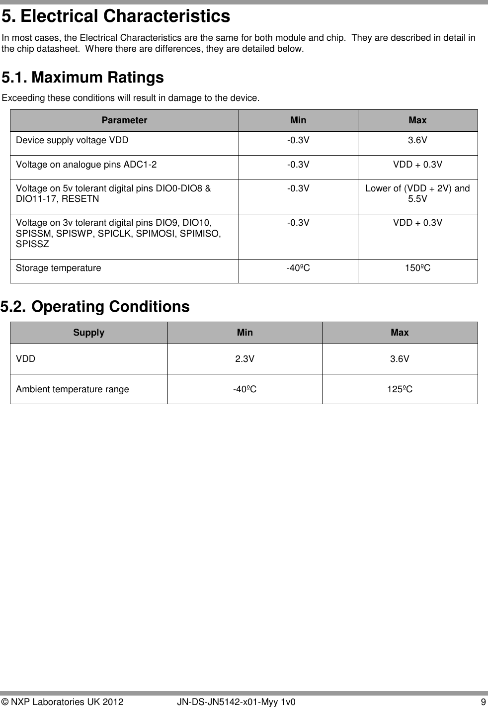
![4 JN-DS-JN5142-x01-Myy 1v0 © NXP Laboratories UK 2012 2. Specifications Most specification parameters for the modules are specified in the chip datasheet - JN-DS-JN5142 Wireless Microcontroller Datasheet, [2]. Where there are differences, the parameters are defined here. VDD=3.0V @ +25°C Typical DC Characteristics Notes JN5142-x01-M00/03 Deep sleep current 100nA Sleep current 0.73uA With active sleep timer Radio transmit current 14.8mA CPU in doze, radio transmitting Radio receive current 16.5mA CPU in doze, radio receiving Centre frequency accuracy +/-25ppm Additional +/-15ppm allowance for temperature and ageing Typical RF Characteristics Notes Receive sensitivity -95dBm Nominal for 1% PER, as per 802.15.4 section 6.5.3.3 (Note 1) Maximum Transmit power +2.5dBm Nominal (Note 1) Maximum input signal +10dBm For 1% PER, measured as sensitivity RSSI range -95 to -10 dBm RF Port impedance – uFl connector 50 ohm 2.4 - 2.5GHz VSWR (max) 2:1 2.4 - 2.5GHz Peripherals Notes Master SPI port 3 selects 250kHz - 16MHz Slave SPI port 250kHz - 8MHz UART 16550 compatible Two-wire serial I/F (compatible with SMbus & I2C) Up to 400kHz Two programmable Timer/Counters with capture/compare facility, Tick timer 16MHz clock Two programmable Sleep Timers 32kHz clock Digital IO lines (multiplexed with UARTs, timers and SPI selects) 18 Four channel Analogue-to-Digital converter 8-bit, up to 100ks/s Programmable analogue comparator Ultra low power mode for sleep Internal temperature sensor and battery monitor The performance of all peripherals is defined in the JN-DS-JN5142 Wireless Microcontroller Datasheet [2] Note 1: Sensitivity is defined for conducted measurements on connectorised modules. Modules with an integrated antenna have approximately 3 dB less e.i.r.p and reciprocal receive sensitivity.](https://usermanual.wiki/NXP-Laboratories-UK/JN5142M0.User-Datasheet/User-Guide-1655320-Page-4.png)
![© NXP Laboratories UK 2012 JN-DS-JN5142-x01-Myy 1v0 5 3. Product Development NXP supplies all the development tools and networking stacks needed to enable end-product development to occur quickly and efficiently. These are all freely available from www.nxp.com/jennic. A range of evaluation/developer kits is also available, allowing products to be quickly bread boarded. Efficient development of software applications is enabled by the provision of a complete, unlimited, software developer kit. Together with the available libraries for the IEEE802.15.4 MAC and the JenNet-IP and RF4CE network stacks, this package provides everything required to develop application code and to trial it with hardware representative of the final module. The modules can be user programmed both in development and in production using software supplied by NXP. Access to the on-chip peripherals, MAC and network stack software is provided through specific APIs. This information is available on the NXP/Jennic support website, together with many example applications, user guides, reference manuals and application notes. 3.1. JN5142 Single Chip Wireless Microcontroller The JN5142-x01-Myy series is constructed around the JN5142-x01 single chip wireless microcontroller, which includes the radio system, a 32-bit RISC CPU, ROM and RAM memory and a range of analogue and digital peripherals. The chip is described fully in JN-DS-JN5142 Wireless Microcontroller Datasheet [2]. The module also includes a 1Mbit serial flash memory, which holds the application code that is loaded into the JN5142 during the boot sequence and provides static data storage, required by the application.](https://usermanual.wiki/NXP-Laboratories-UK/JN5142M0.User-Datasheet/User-Guide-1655320-Page-5.png)
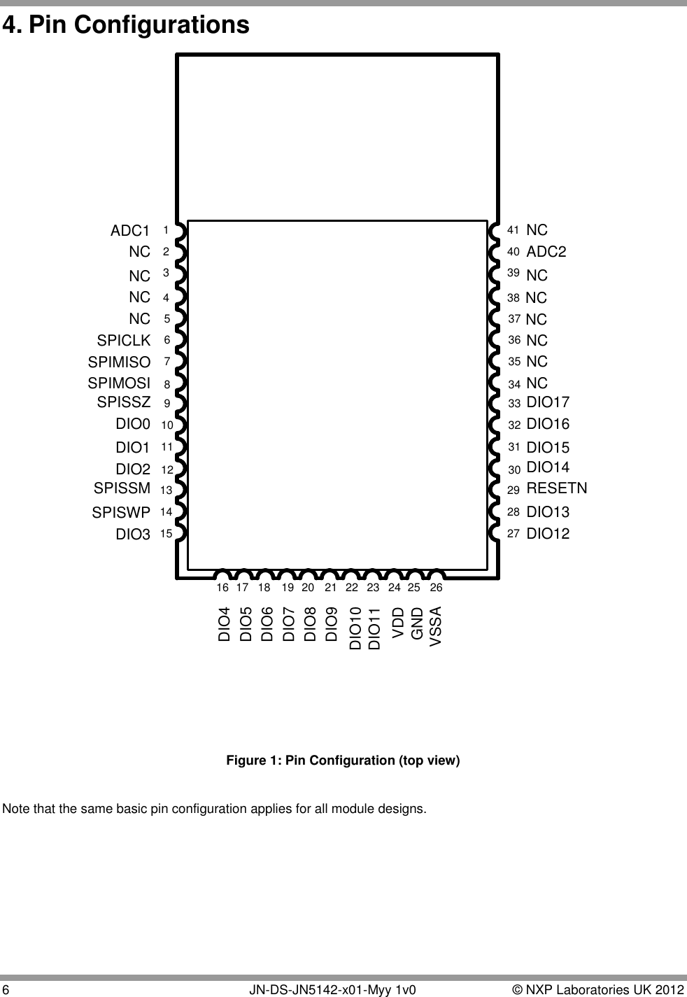
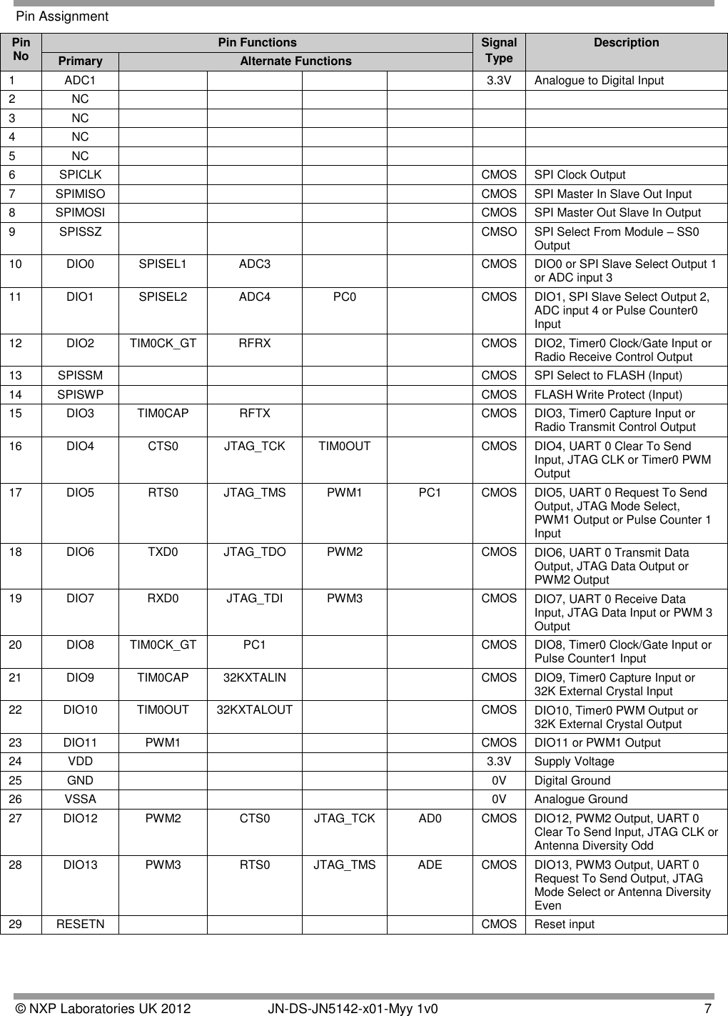
![8 JN-DS-JN5142-x01-Myy 1v0 © NXP Laboratories UK 2012 30 DIO14 SIF_CLK TXD0 JTAG_TDO SPISEL1 CMOS DIO14, Serial Interface Clock, UART 0 Transmit Data Output, JTAG Data Output or SPI Slave Select Output 1 31 DIO15 SIF_D RXD0 JTAG_TDI SPISEL2 CMOS DIO15, Serial Interface Data, UART 0 Receive Data Input, JTAG Data Input or SPI Slave Select Output 2 32 DIO16 COMP1P SIF_CLK CMOS DIO16, Comparator Positive Input or Serial Interface clock 33 DIO17 COMP1M SIF_D CMOS DIO17, Comparator Negative Input or Serial Interface Data 34 NC 35 NC 36 NC 37 NC 38 NC 39 NC 40 ADC2 VREF 3.3V Analogue peripheral reference voltage or ADC input 2 41 NC 4.2. Pin Descriptions All pins behave as described in the JN-DS-JN5142 Wireless Microcontroller Datasheet [2], with the exception of the following: 4.2.1 Power Supplies A single power supply pin, VDD is provided. Separate analogue (VSSA) and digital (GND) grounds are provided. These should be connected together at the module pins. 4.2.2 SPI Memory Connections SPISWP is a write protect pin for the serial flash memory. This should be held low to inhibit writes to the flash device. SPISSZ is connected to SPI Slave Select 0 on the JN5142. SPISSM is connected to the Slave Select pin on the memory. This configuration allows the flash memory device to be programmed using an external SPI programmer if required. For programming in this mode, the JN5142 should be held in reset by taking RESETN low. Two suggested flash 1Mbit memory devices that may be used in the module are, the Micron M25P10A and the Winbond W25X10B. The memory can also be programmed over the UART by using the flash programmer software provided by NXP. This is available as part of the Software Developer kit and libraries available from www.nxp.com/jennic. To enter this programming mode, SPIMISO (pin 7) should be held low whilst the chip is reset. Once programming has finished, the chip should be reset, when it will execute the new code downloaded. For normal operation of the module and programming over the UART, SPISSZ should be connected to SPISSM.](https://usermanual.wiki/NXP-Laboratories-UK/JN5142M0.User-Datasheet/User-Guide-1655320-Page-8.png)
![16 JN-DS-JN5142-x01-Myy 1v0 © NXP Laboratories UK 2012 A.5.3 Leader and Trailer A.5.4 Reel Dimensions: All dimensions are in mm. Module type: A B C N W (min) JN5142-x01-M00/03 330 ±1.0 2.2±0.5 13 ±0.2 100 +0.1 44.5 ±0.3 A.6 Related Documents [1] IEEE Std 802.15.4-2003 IEEE Standard for Information Technology – Part 15.4 Wireless Medium Access Control (MAC) and Physical Layer (PHY) Specifications for Low-Rate Wireless Personal Area Networks (LR-WPANs) [2] JN-DS-JN5142 Wireless Microcontroller Datasheet 300 MM300 MM](https://usermanual.wiki/NXP-Laboratories-UK/JN5142M0.User-Datasheet/User-Guide-1655320-Page-16.png)