NXP Laboratories UK JN5168IT00 JN5168-RD6040-IoT Gateway User Manual JN5168 RD6040 Compliance Statements
NXP Laboratories UK Ltd JN5168-RD6040-IoT Gateway JN5168 RD6040 Compliance Statements
Contents
- 1. Manual
- 2. Antenna Data
- 3. compliance statements
compliance statements

JN5168-RD6040 Compliance
Statements
Reference Manual
JN-RM-2067
Revision 1.0
10-Oct-2013

Draft
JN5168-RD6040 Compliance Statements
Reference Manual
2 © NXP Laboratories UK 2013 JN-RM-2067 v1.0

JN5168-RD6040 Compliance Statements
Reference Manual
Draft
JN-RM-2067 v1.0 © NXP Laboratories UK 2013 3
Contents
About this Manual 4
Organisation 4
1 Introduction 5
2 European R&TTE Directive 1999/5/EC Statement 6
3 FCC Compliance 7
3.1.1 FCC Interference Statement 7
3.1.2 Antennas Approved by FCC for use with JN5168-RD6040 7
3.1.3 FCC ID and Product Labelling 8
4 Industry Canada Compliance 9
4.1 Industry Canada Statement 9
4.2 Industry Canada End Product Labelling 9
A1: R&TTE Notified Body Opinion 10
A2: FCC Declaration of Conformity 11
A 2.1: FCC Grant 12
A3: Industry Canada Grant 13

Draft
JN5168-RD6040 Compliance Statements
Reference Manual
4 © NXP Laboratories UK 2013 JN-RM-2067 v1.0
About this Manual
This manual is exclusively concerned with the JN5168-RD6040 IoT Gateway and
contains compliance documentation, declarations, statements and grants for the
FCC and Industry Canada in North America as well as an R&TTE declaration
and Notified Body Opinion for Europe.
Organisation
This manual consists of 4 chapters, as follows:
Chapter 1 Lists the standards applicable to this document and device
Chapter 2 Contains details of the standards applied for the EU region
Chapter 3 Contains details of the standards applied and statements
required for use in the USA
Chapter 4 Contains details of the standards applied and statements
required for use in Canada

JN5168-RD6040 Compliance Statements
Reference Manual
Draft
JN-RM-2067 v1.0 © NXP Laboratories UK 2013 5
1 Introduction
This document contains mandatory statements and declarations for the
standards below:
1. The JN5168-RD6040 has been tested against the requirements 1.1
European R&TTE Directive 1999/5/EC.
2. The JN5168-RD6040 IoT Gateway is compliant with CFR 47 FCC part
15B & CFR 47 FCC part 15C regulations and in accordance to FCC
Public notice DA00-1407. This document contains details on the
conditions applying to this FCC grant and also contains the FCC
Declaration of Conformity.
3. The JN5168-RD6040 is compliant with Industry Canada RSS210 (Issue
8, Annex 8) and Industry Canada ICES-003 for Class B devices The
JN5168-RD6040 has Industry Canada approval.

Draft
JN5168-RD6040 Compliance Statements
Reference Manual
6 © NXP Laboratories UK 2013 JN-RM-2067 v1.0
2 European R&TTE Directive 1999/5/EC Statement
The JN5168-RD6040 has been tested to and is compliant with the following
standards:
Radio EN 300 328 v1.8.1.
EMC, EN 301 489-17 v2.1.1
Basic Safety Assessment (BSA) EN 60950-1:2006
The product is subject to a Notified Body Opinion which may be found in
Appendix A1.
The JN5168-RD6040 was tested and approved for use with the supplied 2dBi
antenna.
Brand
Model Number
Description
Gain
(dBi)
Connector type
1
Aveslink Technology, Inc
E-2410-GC
Vertical - swivel
2
RP-SMA
2
Aveslink Technology, Inc
E-2820-GC
Vertical - swivel
2
RP-SMA
3
Embedded Antenna Design
FBKR35068-RS-KR
Vertical - knuckle antenna
2
RP-SMA
4
Sunlight Technology
SLA-100020108
Vertical - swivel
2
RP-SMA
Table 1: Approved Antennas
! Alternative vertical antennas may be used provided that the
gain of the replacement antenna does not exceed 2dBi.

JN5168-RD6040 Compliance Statements
Reference Manual
Draft
JN-RM-2067 v1.0 © NXP Laboratories UK 2013 7
3 FCC Compliance
The JN5168-RD6040 IoT Gateway is compliant with CFR 47 FCC part 15B &
CFR 47 FCC part 15C regulations and in accordance to FCC Public notice
DA00-1407.
3.1.1 FCC Interference Statement
This equipment has been tested and found to comply with the limits for a Class B
digital device, pursuant to Part 15 of the FCC Rules. These limits are designed to
provide reasonable protection against harmful interference in a residential
installation. This equipment generates, uses, and can radiate radio frequency
energy and, if not installed and used in accordance with the instructions, may
cause harmful interference to radio communications. However, there is no
guarantee that interference will not occur in a particular installation. If this
equipment does cause harmful interference to radio or television reception,
which can be determined by turning the equipment off and on, the user is
encouraged to try to correct the interference by one of the following measures:
Reorient or relocate the receiving antenna.
Increase the separation between the equipment and receiver.
Connect the equipment into an outlet on a circuit different from that to
which the receiver is connected.
Consult the dealer or an experienced radio/TV technician for help.
Operation is subject to the following two conditions: (1) This device may not
cause harmful interference, and (2) this device must accept any interference
received, including interference that may cause undesired operation.
FCC Caution: Any changes or modifications not expressly approved by the party
responsible for compliance could void the user's authority to operate this
equipment.
3.1.2 Antennas Approved by FCC for use with JN5168-RD6040
This device has been designed to operate with the antennas listed in Table 1,
and having a maximum gain of 2 dBi. Alternative vertical antennas may be used
provided that the gain does not exceed 2 dBi. Antennas having a gain greater
than 2 dBi are strictly prohibited for use with this FCC ID.
The required antenna impedance is 50 ohms.
! Alternative vertical antennas may be used provided that the
gain of the replacement antenna does not exceed 2dBi.
JN5168-RD6040 Compliance Statements
Reference Manual
Draft
JN-RM-2067 v1.0 © NXP Laboratories UK 2013 9
4 Industry Canada Compliance
4.1 Industry Canada Statement
This device complies with Industry Canada licence-
exempt RSS standard(s). Operation is subject
to the following two conditions: (1) this device may
not cause interference, and (2) this device must
accept any interference, including interference that
may cause undesired operation of the device.
Le présent appareil est conforme aux CNR d'Industrie
Canada applicables aux appareils radio
exempts de licence. L'exploitation est autorisée aux
deux conditions suivantes : (1) l'appareil ne
doit pas produire de brouillage, et (2) l'utilisateur de
l'appareil doit accepter tout brouillage
radioélectrique subi, même si le brouillage est
susceptible d'en compromettre le fonctionnement.
To reduce potential radio interference to other users, the antenna type and its
gain should be so chosen that the equivalent isotropic radiated power (e.i.r.p.) is
not more than that permitted for successful communication.
This device has been designed to operate with the antennas listed in Table 1,
and having a maximum gain of 2 dBi. Alternative vertical antennas may be used
provided that the gain does not exceed 2 dBi. The required antenna impedance
is 50 ohms.
! Alternative vertical antennas may be used provided that the
gain of the replacement antenna does not exceed 2dBi.
As long as the above condition is met, further transmitter testing will not be
required. However, the OEM integrator is still responsible for testing their end-
product for any additional compliance requirements required with this module
installed (for example, digital device emissions, PC peripheral requirements, etc).
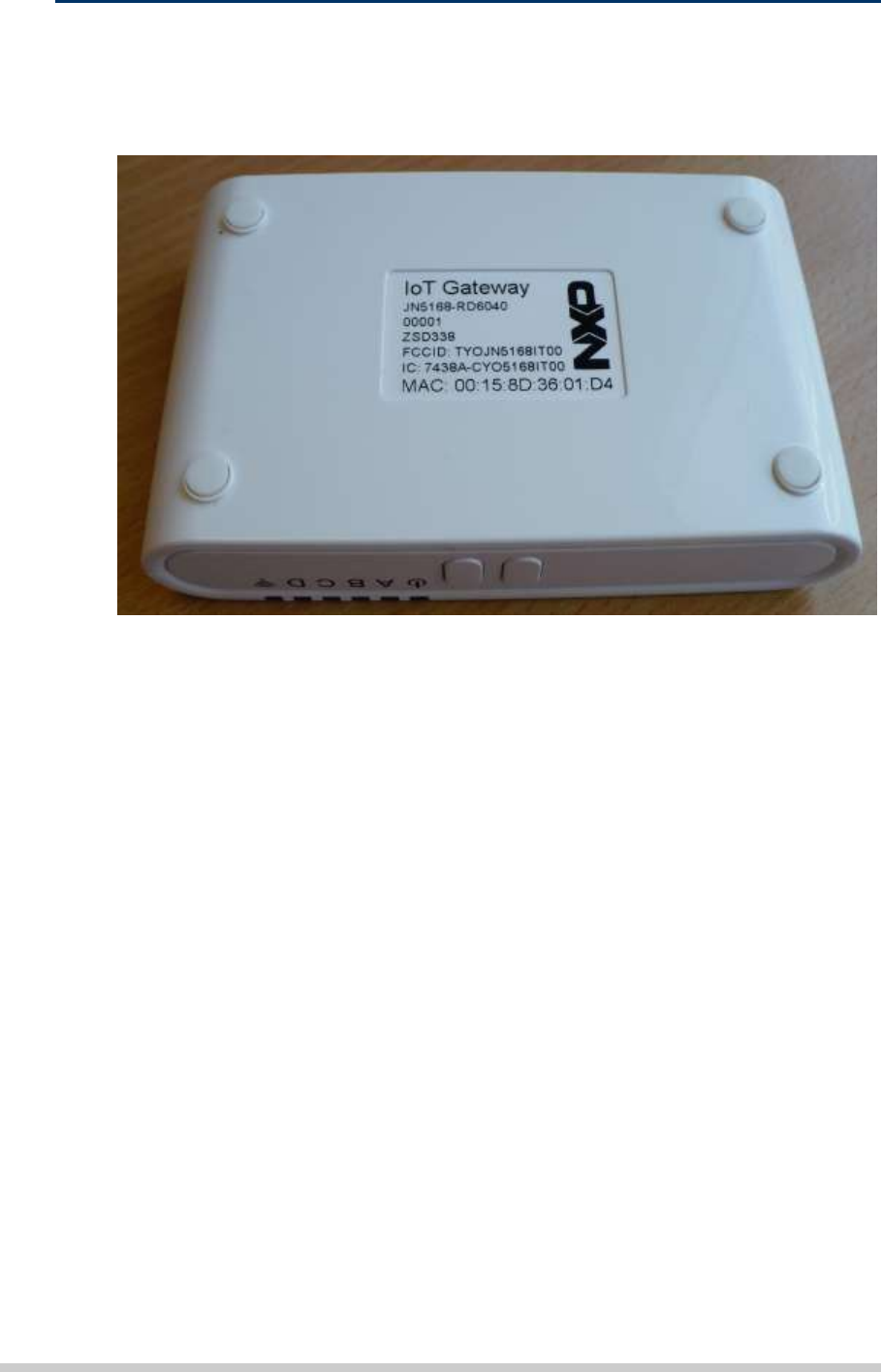
4.2 Industry Canada End Product Labelling
The Industry Canada ID for the JN5168-RD6040 IoT Gateway is
IC: 7438A-CYO5168IT00
This is clearly labelled as shown in Figure 1

Draft
JN5168-RD6040 Compliance Statements
Reference Manual
10 © NXP Laboratories UK 2013 JN-RM-2067 v1.0
A1: R&TTE Notified Body Opinion
The Notified Body Opinion is embedded into this document. To view the
document click the icon below.
TRA-015935 RTTE
NB Opinion.pdf
JN5168-RD6040 Compliance Statements
Reference Manual
Draft
JN-RM-2067 v1.0 © NXP Laboratories UK 2013 11
A2: FCC Declaration of Conformity
JN5139-000-M00
JN5139-000-M01
JN5139-000-M02
JN5139-000-M03
JN5139-000-M04
FCC COMPLIANCE INFORMATION
STATEMENT
DECLARATION OF CONFORMITY
Manufacturer:
NXP Semiconductors Netherlands B.V
Responsible Party in the USA:
Niel P Smith
NXP Semiconductors
411 E. Plumeria Drive
San Jose
CA 95134
USA
Tel 001 408-518 5302
Product:
JN5168-RD6040-IoT-Gateway
Authorisation Procedure:
Declaration of Conformity
This device complies with Part 15 of the FCC Rules. Operation is subject to the following
two conditions: (1) this device may not cause harmful interference, and (2) this device
must accept any interference received, including interference that may cause undesired
operation.
We, NXP Laboratories (UK) Ltd, have determined that the above named equipment has
been shown to comply with the applicable technical standards. Furthermore, we warrant
that each unit of equipment marketed is identical to the unit tested and found acceptable
with the standards. The records maintained continue to reflect the equipment being
produced within the variation that can be expected due to quantity production and testing
on a statistical basis.
NXP Semiconductors BV
JN5168-RD6040-IoT-Gateway
Sheffield, September 24th, 2013
Conrad Farlow, Senior RF Hardware Engineer, NXP Laboratories Ltd
TELEPHONE: +44 (0) 114 281 2655
FACSIMILE: +44 (0) 114 281 2951
E MAIL: info@jennic.com
WEB: www.jennic.com
NXP LABORATORIES (UK) LTD
FURNIVAL STREET
SHEFFIELD
S1 4QT
UNITED KINGDOM

Draft
JN5168-RD6040 Compliance Statements
Reference Manual
12 © NXP Laboratories UK 2013 JN-RM-2067 v1.0
A 2.1: FCC Grant
The FCC grant is embedded into this document. To view the document click the
icon below.
GRANT TO BE EMBEDDED WHEN AVAILABLE

JN5168-RD6040 Compliance Statements
Reference Manual
Draft
JN-RM-2067 v1.0 © NXP Laboratories UK 2013 13
A3: Industry Canada Grant
The Industry Canada grant is embedded into this document. To view the
document click the icon below.
GRANT TO BE EMBEDDED WHEN AVAILABLE

Draft
JN5168-RD6040 Compliance Statements
Reference Manual
14 © NXP Laboratories UK 2013 JN-RM-2067 v1.0
Revision History
Version
Date
Description
1.0
23-Oct-2013
First release

JN5168-RD6040 Compliance Statements
Reference Manual
Draft
JN-RM-2067 v1.0 © NXP Laboratories UK 2013 15
Important Notice
Limited warranty and liability — Information in this document is believed to be accurate and reliable.
However, NXP Semiconductors does not give any representations or warranties, expressed or implied, as to
the accuracy or completeness of such information and shall have no liability for the consequences of use of
such information. NXP Semiconductors takes no responsibility for the content in this document if provided by
an information source outside of NXP Semiconductors.
In no event shall NXP Semiconductors be liable for any indirect, incidental, punitive, special or consequential
damages (including - without limitation - lost profits, lost savings, business interruption, costs related to the
removal or replacement of any products or rework charges) whether or not such damages are based on tort
(including negligence), warranty, breach of contract or any other legal theory.
Notwithstanding any damages that customer might incur for any reason whatsoever, NXP Semiconductors’
aggregate and cumulative liability towards customer for the products described herein shall be limited in
accordance with the Terms and conditions of commercial sale of NXP Semiconductors.
Right to make changes — NXP Semiconductors reserves the right to make changes to information published
in this document, including without limitation specifications and product descriptions, at any time and without
notice. This document supersedes and replaces all information supplied prior to the publication hereof.
Suitability for use — NXP Semiconductors products are not designed, authorized or warranted to be suitable
for use in life support, life-critical or safety-critical systems or equipment, nor in applications where failure or
malfunction of an NXP Semiconductors product can reasonably be expected to result in personal injury, death
or severe property or environmental damage. NXP Semiconductors and its suppliers accept no liability for
inclusion and/or use of NXP Semiconductors products in such equipment or applications and therefore such
inclusion and/or use is at the customer’s own risk.
Applications — Applications that are described herein for any of these products are for illustrative purposes
only. NXP Semiconductors makes no representation or warranty that such applications will be suitable for the
specified use without further testing or modification.
Customers are responsible for the design and operation of their applications and products using NXP
Semiconductors products, and NXP Semiconductors accepts no liability for any assistance with applications or
customer product design. It is customer’s sole responsibility to determine whether the NXP Semiconductors
product is suitable and fit for the customer’s applications and products planned, as well as for the planned
application and use of customer’s third party customer(s). Customers should provide appropriate design and
operating safeguards to minimize the risks associated with their applications and products.
NXP Semiconductors does not accept any liability related to any default, damage, costs or problem which is
based on any weakness or default in the customer’s applications or products, or the application or use by
customer’s third party customer(s). Customer is responsible for doing all necessary testing for the customer’s
applications and products using NXP Semiconductors products in order to avoid a default of the applications
and the products or of the application or use by customer’s third party customer(s). NXP does not accept any
liability in this respect.
Export control — This document as well as the item(s) described herein may be subject to export control
regulations. Export might require a prior authorization from competent authorities.
NXP Laboratories UK Ltd
(Formerly Jennic Ltd)
Furnival Street
Sheffield
S1 4QT
United Kingdom
Tel: +44 (0)114 281 2655
Fax: +44 (0)114 281 2951
For the contact details of your local NXP office or distributor, refer to:
www.nxp.com/jennic