NXP Semiconductors JN5169M0 Wireless microcontroller suitable for Zigbee applications User Manual UM10922
NXP Semiconductors Wireless microcontroller suitable for Zigbee applications UM10922
UserManual.wiki
>
NXP Semiconductors
>
JN5169M0 User Manual
User Manual
Navigation menu
Upload a User Manual
Namespaces
Wiki Guide
HTML
PDF
Info
Views
User Manual
Discussion / Help
Navigation
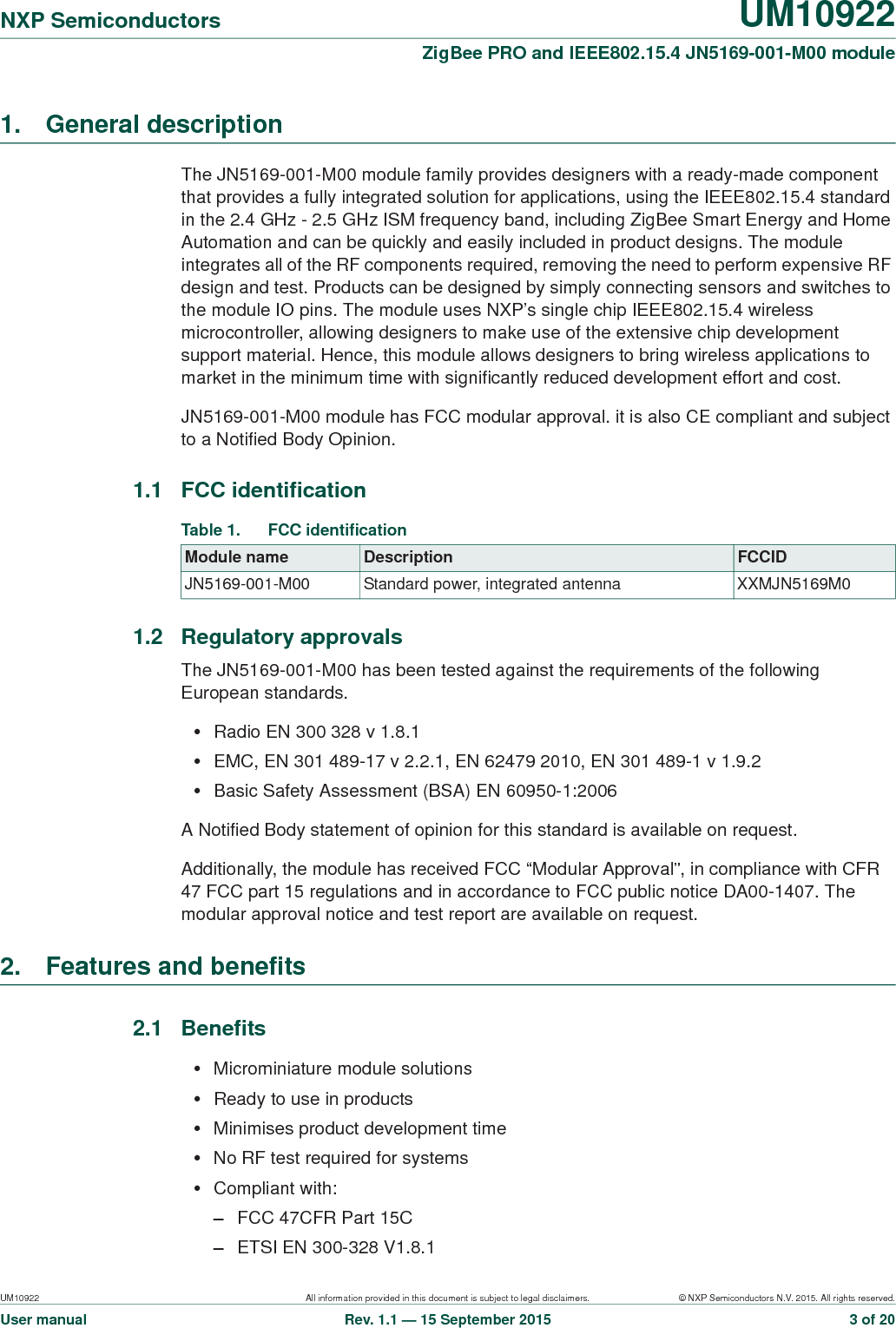
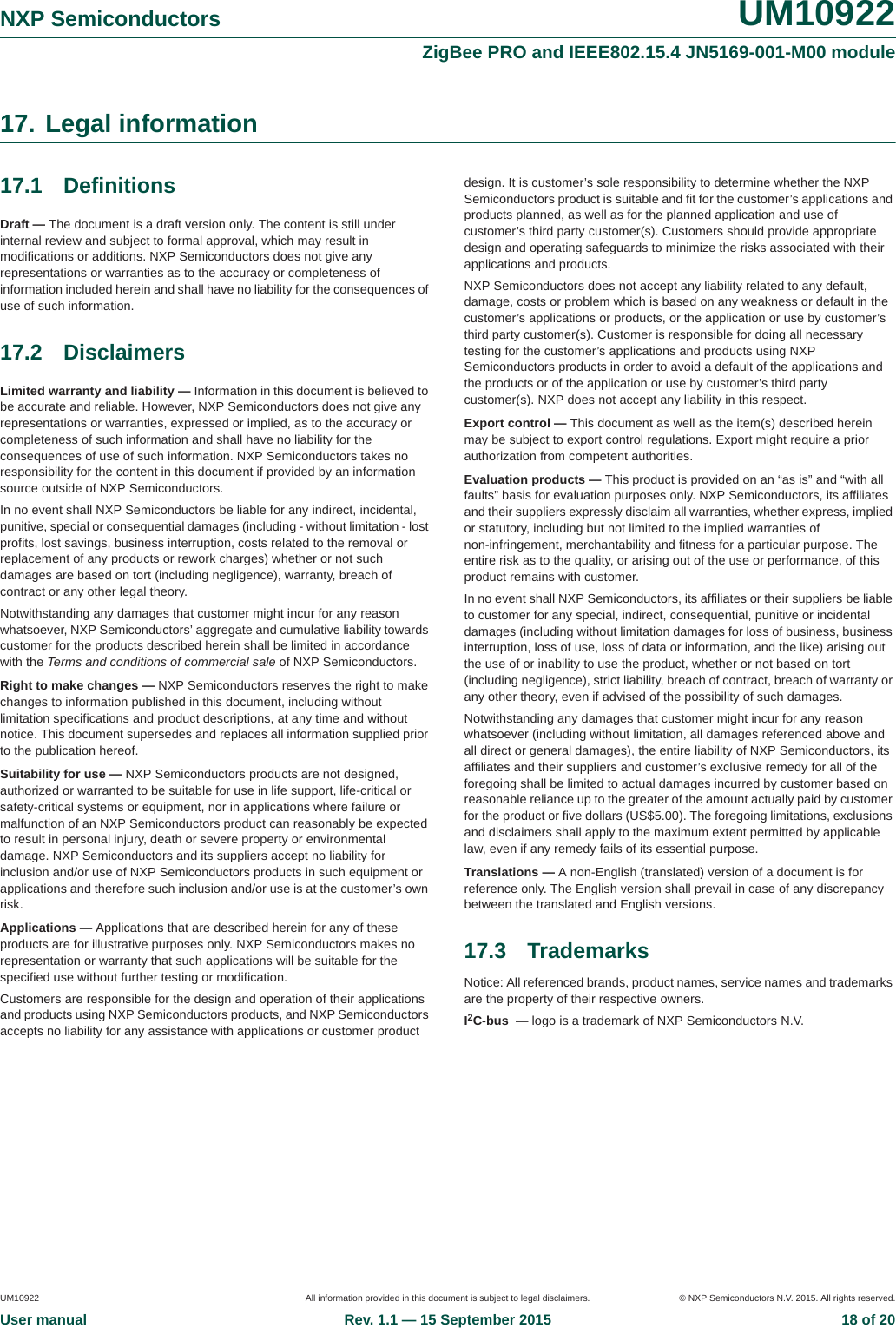
![UM10922 All information provided in this document is subject to legal disclaimers. © NXP Semiconductors N.V. 2015. All rights reserved.User manual Rev. 1.1 — 15 September 2015 7 of 20NXP Semiconductors UM10922ZigBee PRO and IEEE802.15.4 JN5169-001-M00 module7. Pinning information7.1 Pinning7.2 Pin description(1) Multi-function: DIO12/PWM2/CTS0/JTAG_TCK/ADO/SPISMOSI.(2) Multi-function: DIO13/PWM3/RTS0/JTAG_TMS/ADE/SPISMISO.(3) Multi-function: DIO14/SIF_CLK/TXD0/TXD1/JTAG_TDO/SPISEL1/SPISSEL.(4) Multi-function: DIO15/SIF_D/RXD0/RXD1/JTAG_TDI/SPISEL2/SPISCLK.Fig 3. Pin configurationaaa-0190731DIO16/SPISMOSI/SIF_CLK/COMP1P19VDD2DIO17/SPISMISO/SIF_D/COMP1M/PWM4DIO7/RXD0/JTAG_TDI/PWM33RESET_N20DIO6/TXD0/JTAG_TDO/PWM2427DIO5/RTS0/JTAG_TMS/PWM1/PC1526DIO4/CTS0/JTAG_TCK/TIM0OUT/PC0625724DIO19/SPISEL0823DIO18/SPIMOSI922DO1/SPIMISO/PWM321VSS11VREF/ADC2DIO15(4)1213DIO14(3)14DIO13(2)15ADC1DIO12(1)16DIO0/ADO/SPISEL1/ADC317DIO1/ADE/SPISEL2/ADC4/PC0DIO11/PWM1/TXD118DIO2/RFRX/TIM0CK_GT/ADC5DIO10/TIM0OUT/32KXTALOUTDIO3/RFTX/TIM0CAP/ADC6DIO9/TIM0CAP/32KXTALIN/RXD1/32KIN10DO0/SPICLK/PWM2DIO8/TIM0CK_GT/PC1/PWM4Transparent top viewTable 3. Pin descriptionSymbol Pin Type[1] DescriptionADC1 1 I ADC1 — ADC inputDO0/SPICLK/PWM2[2] 2O DO0 — DO0SPICLK — SPI-bus master clock outputPWM2 — PWM2 output](https://usermanual.wiki/NXP-Semiconductors/JN5169M0/User-Guide-2816911-Page-7.png)
![UM10922 All information provided in this document is subject to legal disclaimers. © NXP Semiconductors N.V. 2015. All rights reserved.User manual Rev. 1.1 — 15 September 2015 8 of 20NXP Semiconductors UM10922ZigBee PRO and IEEE802.15.4 JN5169-001-M00 moduleDO1/SPIMISO/PWM3[3] 3I/O DO1 — DO1SPIMISO — SPI-bus Master In, Slave Out inputPWM3 — PWM3 outputDIO18/SPIMOSI 4 I/O DIO18 — DIO18SPIMOSI — SPI-bus Master Out Slave In outputDIO19/SPISEL0 5 I/O DIO19 — DIO19SPISEL0 — SPI-bus Master Select Output 0DIO0/ADO/SPISEL1/ADC3 6 I/O DIO0 — DIO0ADO — antenna diversity odd outputSPISEL1 — SPI-bus master select output 1ADC3 — ADC input: ADC3DIO1/ADE/SPISEL2/ADC4/PC0 7 I/O DIO1 — DIO1ADE — antenna diversity even outputSPISEL2 — SPI-bus master select output 2ADC4 — ADC input: ADC4PC0 — pulse counter 0 inputDIO2/RFRX/TIM0CK_GT/ADC5 8 I/O DIO2 — DIO2RFRX — radio receives control outputTIM0CK_GT — timer0 clock/gate inputADC5 — ADC input: ADC5DIO3/RFTX/TIM0CAP/ADC6 9 I/O DIO3 — DIO3RFTX — radio transmit control outputTIM0CAP — timer0 capture inputADC6 — ADC input: ADC6DIO4/CTS0/JTAG_TCK/TIM0OUT/PC0 10 I/O DIO4 — DIO4CTS0 — UART 0 clear to send inputJTAG_TCK — JTAG CLK inputTIM0OUT — timer0 PWM outputPC0 — pulse counter 0 inputDIO5/RTS0/JTAG_TMS/PWM1/PC1 11 I/O DIO5 — DIO5RTS0 — UART 0 request to send outputJTAG_TMS — JTAG mode select inputPWM1 — PWM1 outputPC1 — pulse counter 1 inputDIO6/TXD0/JTAG_TDO/PWM2 12 I/O DIO6 — DIO6TXD0 — UART 0 transmit data outputJTAG_TDO — JTAG data outputPWM2 — PWM2 data outputTable 3. Pin description …continuedSymbol Pin Type[1] Description](https://usermanual.wiki/NXP-Semiconductors/JN5169M0/User-Guide-2816911-Page-8.png)
![UM10922 All information provided in this document is subject to legal disclaimers. © NXP Semiconductors N.V. 2015. All rights reserved.User manual Rev. 1.1 — 15 September 2015 9 of 20NXP Semiconductors UM10922ZigBee PRO and IEEE802.15.4 JN5169-001-M00 moduleDIO7/RXD0/JTAG_TDI/PWM3 13 I/O DIO7 — DIO7RXD0 — UART 0 receive data inputJTAG_TDI — JTAG data inputPWM3 — PWM 3 data outputDIO8/TIM0CK_GT/PC1/PWM4 14 I/O DIO8 — DIO8TIM0CK_GT — timer0 clock/gate inputPC1 — pulse counter1 inputPWM4 — PWM 4 outputDIO9/TIM0CAP/32KXTALIN/RXD1/32KIN 15 I/O DIO9 — DIO9TIM0CAP — Timer0 Capture input32KXTALIN — 32 kHz External Crystal inputRXD1 — UART1 Receive Data input32KIN — 32 kHz External clock inputDIO10/TIM0OUT/32KXTALOUT 16 I/O DIO10 — DIO10TIM0OUT — Timer0 PWM Output32KXTALOUT — 32 kHz External Crystal outputVDD 17 P VDD — supply voltageVSS 18 GND groundDIO11/PWM1/TXD1 19 I/O DIO11 — DIO11PWM1 — PWM1 outputTXD1 — UART1 Transmit Data outputDIO12[4] 20 I/O DIO12 — DIO12PWM2 — PWM2 outputCTS0 — UART0 clear to send inputJTAG_TCK — JTAG CLK inputADO — antenna diversity odd outputSPISMOSI — SPI-bus slave Master Out, Slave In inputDIO13[5] 21 I/O DIO13 — DIO13PWM3 — PWM3 outputRTS0 — UART0 request to send outputJTAG_TMS — JTAG mode select inputADE — antenna diversity even outputSPISMISO — SPI-bus slave master in slave out outputRESET_N 22 I RESET_N — reset inputDIO14[6] 23 I/O DIO14 — DIO14SIF_CLK — serial interface clockTXD0 — UART 0 transmit data outputTXD1 — UART 1 transmit data outputJTAG_TDO — JTAG data outputSPISEL1 — SPI-bus master select output 1SPISSEL — SPI-bus slave select inputTable 3. Pin description …continuedSymbol Pin Type[1] Description](https://usermanual.wiki/NXP-Semiconductors/JN5169M0/User-Guide-2816911-Page-9.png)
![UM10922 All information provided in this document is subject to legal disclaimers. © NXP Semiconductors N.V. 2015. All rights reserved.User manual Rev. 1.1 — 15 September 2015 10 of 20NXP Semiconductors UM10922ZigBee PRO and IEEE802.15.4 JN5169-001-M00 module[1] P = power supply; G = ground; I = input, O = output; I/O = input/output.[2] JTAG programming mode: must be left floating high during reset to avoid entering JTAG programming mode.[3] UART programming mode: leave pin floating high during reset to avoid entering UART programming mode or hold it low to program.[4] Multi-function: DIO12/PWM2/CTS0/JTAG_TCK/ADO/SPISMOSI.[5] Multi-function: DIO13/PWM3/RTS0/JTAG_TMS/ADE/SPISMISO.[6] Multi-function: DIO14/SIF_CLK/TXD0/TXD1/JTAG_TDO/SPISEL1/SPISSEL.[7] Multi-function: DIO15/SIF_D/RXD0/RXD1/JTAG_TDI/SPISEL2/SPISCLK.8. Functional description8.1 JN5169 single chip wireless microcontrollerThe JN5169-001-M00 is constructed around the JN5169-001 single chip wireless microcontroller, which includes the radio system, a 32-bit RISC CPU, Flash, RAM and EEPROM memory and a range of analogue and digital peripherals.The chip is described fully in JN5169 Wireless Microcontroller Datasheet (see Ref. 2).8.2 PeripheralsDIO15[7] 24 I/O DIO15 — DIO15SIF_D — serial interface dataRXD0 — UART 0 receive data inputRXD1 — UART 1 receive data inputJTAG_TDI — JTAG data inputSPISEL2 — SPI-bus master select output 2SPISCLK — SPI-bus slave clock inputDIO16/SPISMOSI/SIF_CLK/COMP1P 25 I/O DIO16 — DIO16COMP1P — comparator positive inputSIF_CLK — Serial Interface clockSPISMOSI — SPI-bus Slave Master Out Slave In inputDIO17/SPISMISO/SIF_D/COMP1M 26 I/O DIO17 — DIO17COMP1M — COMP1M; comparator negative inputSIF_D — Serial Interface DataSPISMISO — SPI-bus Slave Master In Slave Out outputPWM4 — PWM 4 outputVREF/ADC2 27 P VREF — analog peripheral reference voltageIADC2 — ADC input 2Table 3. Pin description …continuedSymbol Pin Type[1] DescriptionTable 4. PeripheralsPeripherals JN5169-001-M00 JN5169-001-M06 NotesMaster SPI-bus port 3 selects 3 selects 250 kHz - 16 MHzSlave SPI-bus port 1 1 250 kHz - 4 MHzUART 2 2 16550 compatible](https://usermanual.wiki/NXP-Semiconductors/JN5169M0/User-Guide-2816911-Page-10.png)
![UM10922 All information provided in this document is subject to legal disclaimers. © NXP Semiconductors N.V. 2015. All rights reserved.User manual Rev. 1.1 — 15 September 2015 12 of 20NXP Semiconductors UM10922ZigBee PRO and IEEE802.15.4 JN5169-001-M00 module10. Recommended operating conditions[1] To reach the maximum TX power, 2.8 V is the minimum.11. Characteristics11.1 DC current[1] To reach the maximum TX power, 2.8 V is the minimum.[1] Waiting on I/O event.VIO(dig) digital input/output voltage 0.3 VDDD +0.3VVTstg storage temperature 40 +150 qCVESD electrostatic discharge voltage according to ETSI EN 301 489-17 2012 V2.2.1 and ETSI EN 301 489-1 2011 V1.9.2-4kVTable 5. Limiting values …continuedSymbol Parameter Conditions Min Max UnitTable 6. Operating conditionsSymbol Parameter Conditions Min Max UnitVDD supply voltage [1] 23.6VTamb ambient temperature standard range 40 +85 qCTable 7. Active processingVDD =2V to 3.6V; Tamb =25qC; unless otherwise specified.Symbol Parameter Conditions Min Typ Max UnitIDD supply current M00radio in receive mode; maximum input level at 10 dBm - 17.8 - mAradio in receive mode; maximum input level at 0 dBm - 16.7 - mAradio in transmit mode 10 dBm [1] - 25.7 - mAradio in transmit mode 8.5 dBm [1] - 23.5 - mATable 8. Sleep modeVDD =2V to 3.6V; Tamb =25qC; unless otherwise specified.Symbol Parameter Conditions Min Typ Max UnitIDD(IO) input/output supply currentin sleep mode; with I/O wake-up; Tamb =25°C[1] -0.10-PAin sleep mode; with I/O and RC oscillator timer wake-up; Tamb =25qC-0.73-PATable 9. Deep sleep modeVDD =2V to 3.6V; Tamb =25qC; unless otherwise specified.Symbol Parameter Conditions Min Typ Max UnitIDD supply current deep sleep mode; measured at 25 qC[1] -50-nA](https://usermanual.wiki/NXP-Semiconductors/JN5169M0/User-Guide-2816911-Page-12.png)
![UM10922 All information provided in this document is subject to legal disclaimers. © NXP Semiconductors N.V. 2015. All rights reserved.User manual Rev. 1.1 — 15 September 2015 13 of 20NXP Semiconductors UM10922ZigBee PRO and IEEE802.15.4 JN5169-001-M00 module[1] Waiting on chip RESET or I/O event.11.2 AC characteristics11.2.1 Radio transceiverThese modules meet all the requirements of the IEEE802.15.4 standard over 2.0 V to 3.6 V and offers the improved RF characteristics shown in Table 10. All RF characteristics are measured single ended.[1] With external matching inductors and assuming PCB layout.[1] To reach the maximum TX power, 2.8 V is the minimum on VDDA.[2] Up to an extra 2.5 dB of attenuation is available if required.12. Federal Communication Commission Statement•This equipment has been tested and found to comply with the limits for a Class B digital device, pursuant to Part 15 of the FCC Rules see Ref. 4. These limits are designed to provide reasonable protection against harmful interference in a residential installation. This equipment generates, uses, and can radiate radio frequency energy and, if not installed and used in accordance with the instructions, may cause harmful interference to radio communications. However, there is no guarantee that interference will not occur in a particular installation. If this equipment Table 10. RF port characteristicsSingle-ended; Impedance = 50 :[1]; VDD =2V to 3.6V; Tamb =25qC; unless otherwise specified.Symbol Parameter Conditions Min Typ Max Unitfrange frequency range 2.4 - 2.485 GHzTable 11. Radio transceiver characteristicsVDD =2V to 3.6V; Tamb =25qC; unless otherwise specified.Symbol Parameter Conditions Min Typ Max UnitReceiverSRX receiver sensitivity nominal for 1 % PER, as per 802.15.4 - 96.5 - dBmPi(RX)(max) maximum receiver input power1 % PER, measured as sensitivity; supply current at 14.7 mA-10-dBm1 % PER, measured as sensitivity; supply current at 13 mA-0-dBmRSSI(min) minimum received signal strength indicator-95 - dBmRSSI(max) maximum received signal strength indicator-10 - dBmTransmitterPooutput power IDD = 23.3 mA [1] -10-dBmIDD = 19.6 mA [1] -8.5-dBmPo(cr) control range output powerin 6 major steps and then 4 fine steps [2] -42 - dB](https://usermanual.wiki/NXP-Semiconductors/JN5169M0/User-Guide-2816911-Page-13.png)
![UM10922 All information provided in this document is subject to legal disclaimers. © NXP Semiconductors N.V. 2015. All rights reserved.User manual Rev. 1.1 — 15 September 2015 17 of 20NXP Semiconductors UM10922ZigBee PRO and IEEE802.15.4 JN5169-001-M00 module15. Abbreviations16. References[1] IEEE Std 802.15.4-2011 — IEEE Std 802.15.4-2011 IEEE Standard for Information Technology.[2] JN5169 — JN5169 wireless microcontroller datasheet.[3] Wireless Connectivity TechZone — http://www.nxp.com/techzones/wireless-connectivity[4] Part 15 of the FCC Rules — http://www.ecfr.gov/cgiͲbin/textͲidx?SID=d01e00935bfcb0d53b914e7c8e63f383&node=47:1.0.1.1.16&rgn=div5Table 12. AbbreviationsAcronym DescriptionAPI Application Program InterfaceADC Analog to Digital ConverterFCC Federal Communication CommissionIO Input OutputOEM Original Equipment ManufacturerPCB Printed Circuit BoardPER Packet Error RatePWM Pulse Width ModulationR&TTE Radio and Telecommunications Terminal EquipmentRF Radio FrequencyRISC Reduce Instruction Set ComputingRSSI Receive Signal Strength IndicatorRTS Request-To-SendSPI Serial Peripheral InterfaceSVM Supply Voltage MonitorSYNTH SYNTHesizerUART Universal Asynchronous Receiver/Transmitter](https://usermanual.wiki/NXP-Semiconductors/JN5169M0/User-Guide-2816911-Page-17.png)