NXP Semiconductors JN5179M1X ZigBee Modular Transmitter User Manual UM11018
NXP Semiconductors ZigBee Modular Transmitter UM11018
UserManual.wiki
>
NXP Semiconductors
>
JN5179M1X User Manual
User Manual
Navigation menu
Upload a User Manual
Namespaces
Wiki Guide
HTML
PDF
Info
Views
User Manual
Discussion / Help
Navigation
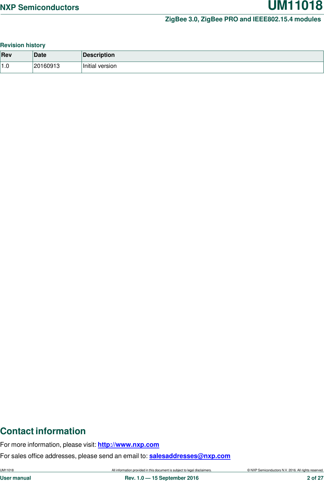
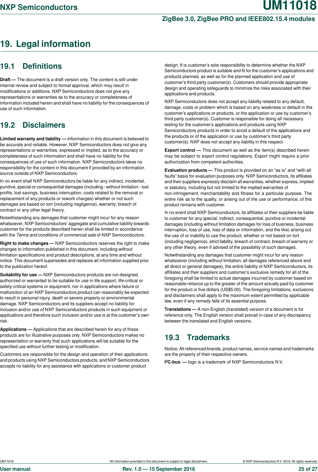
![UM11018 NXP Semiconductors UM11018 User manual All information provided in this document is subject to legal disclaimers. Rev. 1.0 — 15 September 2016 © NXP Semiconductors N.V. 2016. All rights reserved. 8 of 27 ZigBee 3.0, ZigBee PRO and IEEE802.15.4 modules 8. Pinning information 8.1 Pinning 8.2 Pin description Table 3. Pin description Symbol Pin Type[1] Description DIO2 1 IO DIO2 — digital input/output 2 ADC5 — ADC input 5 SDA — I2C-bus master/slave SDA input/output (push-pull output) RXD1 — UART 1 receive data input TIM0CAP — Timer0 capture input RFRX — radios receiver control output ADC0 2 I ADC0 — ADC input 0 DIO2 1 ADC0 2 DIO0(1) 3 DIO1(2) 4 DIO3 5 DIO4 6 DIO10/RXD0 7 DIO9/TXD0 8 DIO8 9 27 ADC1 26 DIO18 25 DIO15 24 RESET_N23 DIO14 22 DIO13 21 DIO12 20 n.c. 19 DIO5 Transparent top view aaa-023363(1) DIO0 pin of the JN5179-001-M16 is not connected to DIO0 pin of the JN5179. The DIO0 of the module is LNA_BYPASS. (2) DIO1 pin of the JN5179-001-M16 is not connected to DIO1 pin of the JN5179. The DIO1 of the module is ANT_SEL. Fig 3. Pin configuration DIO7/SPIMOSI 10 DIO6/SPISEL0 11 DO1/SPIMISO 12 DO0/SPICLK 13 DIO17 14 DIO11 15 n.c. 16 VSS VDDD 17 18](https://usermanual.wiki/NXP-Semiconductors/JN5179M1X/User-Guide-3148661-Page-8.png)
![UM11018 NXP Semiconductors UM11018 User manual All information provided in this document is subject to legal disclaimers. Rev. 1.0 — 15 September 2016 © NXP Semiconductors N.V. 2016. All rights reserved. 9 of 27 ZigBee 3.0, ZigBee PRO and IEEE802.15.4 modules Table 3. Pin description …continued Symbol Pin Type[1] Description DIO0[2] 3 DIO0 — digital input/output 0 ADC4 — ADC input 4 SPISEL0 — SPI-bus master select output 0 RFRX — radio receiver control output FLICK_CTRL — flicker control output ADO — antenna diversity odd output DIO1[2] 4 IO DIO1 — digital input/output 1 ADC3 — ADC input 3 RFTX — radio transmitter control input PC0 — pulse counter 0 input ADE — antenna diversity even output DIO3 5 IO DIO3 — digital input/output 3 ADC2 — ADC input 2 PWM4 — PWM4 output SCL — I2C-bus master/slave SCL input/output (push-pull output) TXD1 — UART 1 transmit data output TIM0OUT — Timer0 output RFTX — radio transmit control input FLICK_CTRL — flicker control output DIO4 6 IO DIO4 — digital input/output 4 SCL — I2C-bus master/slave SCL input/output (open-drain) RXD0 — UART 0 receive data input TIM0CK_GT — Timer0 clock/gate input ADO — antenna diversity odd output DIO10/RXD0 7 IO DIO10 — digital input/output 10 JTAG_TDI — JTAG TDI data input RXD0 — UART 0 receive data input DIO9/TXD0 8 IO DIO9 — digital input/output 9 JTAG_TDO — JTAG TDO data output TXD0 — UART 0 transmit data output TRACESWV — ARM trace serial wire viewer output DIO8 9 IO DIO8 — digital input/output 8 PWM5 — PWM5 output TIM0OUT — Timer0 output TRACECLK — trace clock output 32KXTALIN — 32 kHz clock input](https://usermanual.wiki/NXP-Semiconductors/JN5179M1X/User-Guide-3148661-Page-9.png)
![UM11018 NXP Semiconductors UM11018 User manual All information provided in this document is subject to legal disclaimers. Rev. 1.0 — 15 September 2016 © NXP Semiconductors N.V. 2016. All rights reserved. 10 of 27 ZigBee 3.0, ZigBee PRO and IEEE802.15.4 modules Table 3. Pin description …continued Symbol Pin Type[1] Description DIO7/SPIMOSI 10 IO DIO7 — digital input/output 7 SPIMOSI — SPI-bus master data output JTAG_TDI — JTAG TDI data input SPISEL2 — SPI-bus master select output 2 SPISSEL — SPI-bus slave select input CMP_OUT — comparator output 32KIN — 32 kHz External clock input 32KXTALOUT — 32 kHz clock output DIO6/SPISEL0 11 IO DIO6 — digital input/output 6 SPISEL0 — SPI-bus master select output 0 CTS0 — UART 0 clear to send input RXD1 — UART 1 receive data input JTAG_TCK — JTAG TCK input SWCK — Serial Wire Debugger Clock input SPISCLK — SPI-bus slave clock input TIM1CAP — Timer1 capture input DO1/SPIMISO[3] 12 IO DO1 — digital output 1 SPIMISO — SPI-bus master data input SPISMISO — SPI-bus slave data output ADO — antenna diversity odd output DO0/SPICLK[4] 13 O DO0 — digital output 0 SPICLK — SPI-bus master clock output ADE — antenna diversity even output DIO17 14 IO DIO17 — digital input/output 17 JTAG_TCK — JTAG TCK input SWCK — Serial Wire Debugger Clock input SPISEL0 — SPI-bus master select output 0 TIM1CAP — Timer1 capture input COMP1P — comparator plus input SPISMISO — SPI-bus slave data output DIO11 15 IO DIO11 — digital input/output 11 JTAG_TMS — JTAG TMS input SWD — serial wire debugger input RTS0 — UART 0 request to send output TXD1 — UART 1 transmit data output SPICLK — SPI-bus master clock output SPISMOSI — SPI-bus slave data input TIM1OUT — Timer1 output TRACED0 — ARM trace data0 output n.c. 16 - not connected; keep floating or ground VSS 17 G VSS — ground](https://usermanual.wiki/NXP-Semiconductors/JN5179M1X/User-Guide-3148661-Page-10.png)
![UM11018 NXP Semiconductors UM11018 User manual All information provided in this document is subject to legal disclaimers. Rev. 1.0 — 15 September 2016 © NXP Semiconductors N.V. 2016. All rights reserved. 11 of 27 ZigBee 3.0, ZigBee PRO and IEEE802.15.4 modules Table 3. Pin description …continued Symbol Pin Type[1] Description VDDD 18 P VDDD — digital supply voltage DIO5[5] 19 IO DIO5 — digital input/output 5 SDA — I2C-bus master/slave SDA input/output (open-drain) TXD0 — UART 0 transmit data output PC1 — pulse counter 1 input TIM0CAP — Timer0 capture input n.c. 20 - not connected; keep floating or ground DIO12 21 IO DIO12 — digital input/output 12 PWM1 — PWM1 output TXD0 — UART 0 transmit data output TRACED3 — ARM trace data3 output DIO13 22 IO DIO13 — digital input/output 13 PWM2 — PWM2 output RXD0 — UART 0 receive data input PC0 — pulse counter 0 input TRACED2 — ARM trace data2 output DIO14 23 IO DIO14 — digital input/output 14 PWM3 — PWM3 output PC1 — pulse counter 1 input CMP_OUT — comparator output TRACED1 — ARM trace data1 output SPISMOSI — SPI-bus slave data input RESET_N 24 IO RESET_N — reset input DIO15 25 IO DIO15 — digital input/output 15 PWM6 — PWM6 output JTAG_TDO — JTAG TDO data output SPIMOSI — SPI-bus master data output SPISEL1 — SPI-bus master select output 1 TIM0CK_GT — Timer0 - clock gate input TRACESWV — ARM trace Serial Wire Viewer output SPISSEL — SPI-bus slave select input DIO18 26 IO DIO18 — digital input/output 18 JTAG_TMS — JTAG TMS input SWD — Serial Wire Debugger input SPIMISO — SPI-bus master data input TIM1OUT — Timer1 output COMP1M — comparator minus input SPISCLK — SPI-bus slave clock input ADC1 27 I VREF — analog peripheral reference voltage ADC1 — ADC input 1](https://usermanual.wiki/NXP-Semiconductors/JN5179M1X/User-Guide-3148661-Page-11.png)
![UM11018 NXP Semiconductors UM11018 User manual All information provided in this document is subject to legal disclaimers. Rev. 1.0 — 15 September 2016 © NXP Semiconductors N.V. 2016. All rights reserved. 12 of 27 ZigBee 3.0, ZigBee PRO and IEEE802.15.4 modules [1] P = power supply; G = ground; I = input, O = output; IO = input/output. [2] Not available on the JN5179-001-M16 since they are used to control the front-end module. DIO0 of the module is LNA_BYPASS and the DIO1 of the module is ANT_SEL. [3] UART programming mode: leave pin floating high during reset to avoid entering UART programming mode or hold it low to program. [4] JTAG programming mode: must be left floating high during reset to avoid entering JTAG programming mode. [5] Open-drain. 9. Functional description 9.1 JN5179 single chip wireless microcontroller The JN5179-001-M1x series is constructed around the JN5179-001 single chip wireless microcontroller, which includes the radio system, an ARM Cortex-M3 CPU, Flash, RAM and EEPROM memory and a range of analog and digital peripherals. The chip is described fully in JN5179 Wireless Microcontroller Datasheet (see Ref. 2). 9.2 Peripherals Table 4. Peripherals description Peripherals JN5179-001-M10 JN5179-001-M13 JN5179-001-M16 Notes Master SPI-bus port 3 selects 3 selects 3 selects 250 kHz - 16 MHz Slave SPI-bus port 1 1 1 250 kHz - 4 MHz UART 2 2 2 16550 compatible Two-wire serial I/F (compatible with SMbus and I2C-bus) 1 1 1 Up to 400 kHz PWM 16 MHz clock timer 4 4 4 timer/counter 1 1 1 Programmable Sleep Timers 2 2 2 32 kHz clock Digital IO lines (multiplexed with UARTs, timers and SPI-bus selects) 20 20 18 DIO2 and DIO3 are not available on JN5179-001-M16 modules Analog-to-Digital converter 4 4 4 10 bit, up to 100 ks/s Programmable analog comparator 1 1 1 ultra low-power mode for sleep Internal temperature sensor 1 1 1 Internal battery sensor 1 1 1 The performance of all peripherals is defined in the JN5179 Wireless Microcontroller Datasheet (see Ref. 2). NXP supplies all the development tools and networking stacks needed to enable end-product development to occur quickly and efficiently. These are all freely available from the NXP Wireless Connectivity TechZone (see Ref. 3). A range of evaluation/developer kits is also available, allowing products to be quickly bread boarded.](https://usermanual.wiki/NXP-Semiconductors/JN5179M1X/User-Guide-3148661-Page-12.png)
![UM11018 NXP Semiconductors UM11018 User manual All information provided in this document is subject to legal disclaimers. Rev. 1.0 — 15 September 2016 © NXP Semiconductors N.V. 2016. All rights reserved. 13 of 27 ZigBee 3.0, ZigBee PRO and IEEE802.15.4 modules Efficient development of software applications is enabled by the provision of a complete, unlimited, software developer kit. Together with the available libraries for the IEEE802.15.4 MAC and ZigBee PRO network stacks, this package provides everything required to develop application code and to trial it with hardware representative of the final module. The modules can be user programmed both in development and in production using software supplied by NXP. Access to the on-chip peripherals, MAC and network stack software is provided through specific APIs. This information is available on the NXP support website, together with many example applications, user guides, reference manuals and application notes. 9.3 JN5179-001-M16 Antenna diversity ANT_SEL is used to select between the two antennas on the M16 module. Leaving ANT_SEL unconnected or connecting to VCC selects the printed antenna. Tying ANT_SEL to ground selects the µFL connector. The module can also be used in antenna diversity solutions where the module will automatically swap between the two antennas in order to achieve the best radio performance. This can be done connecting ANT_SEL to DIO4, DIO5, DO0 or DO1 depend upon your application. The antenna diversity functionality can be enabled by calling vAHI_AntennaDiversityEnable. The DIO can be selected using vAHI_SetDIOpinMultiplexValue. Please see JN-UG-3118-JN517x-Integrated-Peripherals-API for more details. The LNA bypass signal can be used to switch off the LNA in the frontend. This can be useful when in the presence of strong Wifi signals that can overload the frontend. If the pin is left unconnected or tied to VCC then the LNA is enabled. If the signal is tied to ground then the LNA will be bypassed during RX. The signal can be connected to a DIO to give software control over the LNA if required. 10. Limiting values Table 5. Limiting values Symbol Parameter Conditions Min Max Unit VDD supply voltage −0.3 +3.6 V VADC0 voltage on pin ADC0 −0.3 VDD + 0.3 V V VADC1 voltage on pin ADC1 −0.3 VDD + 0.3 V V VIO(dig) digital input/output voltage −0.3 VDD + 0.3 V V Tstg storage temperature −40 +150 °C 11. Recommended operating conditions Table 6. Operating conditions Symbol Parameter Conditions Min Max Unit VDD supply voltage [1] 2 3.6 V Tamb ambient temperature standard range −40 +85 °C](https://usermanual.wiki/NXP-Semiconductors/JN5179M1X/User-Guide-3148661-Page-13.png)
![UM11018 NXP Semiconductors UM11018 User manual All information provided in this document is subject to legal disclaimers. Rev. 1.0 — 15 September 2016 © NXP Semiconductors N.V. 2016. All rights reserved. 14 of 27 ZigBee 3.0, ZigBee PRO and IEEE802.15.4 modules [1] To reach the maximum TX power, 2.8 V is the minimum. 12. Characteristics 12.1 DC current Table 7. Active processing VDD = 2 V to 3.6 V; Tamb = −40 °C to +85 °C; unless otherwise specified. Symbol Parameter Conditions Min Typ Max Unit IDD supply current M10 radio in receive mode; maximum input level at –2 dBm - 16.6 - mA radio in transmit mode 10 dBm [1] - 26.2 - mA radio in transmit mode 8.5 dBm [1] - 22.6 - mA M13 radio in receive mode; maximum input level at –2 dBm - 16.6 - mA radio in transmit mode 10 dBm [1] - 26.2 - mA radio in transmit mode 8.5 dBm [1] - 22.6 - mA M16 radio in receive mode - 16.6 - mA radio in transmit mode [1] - 125 - mA [1] To reach the maximum TX power, 2.8 V is the minimum. Table 8. Sleep mode VDD = 2 V to 3.6 V; Tamb = −40 °C to +85 °C; unless otherwise specified. Symbol Parameter Conditions Min Typ Max Unit IDD(IO) input/output supply current in sleep mode; with I/O and RC oscillator timer wake-up; Tamb = 25 °C - 0.73 - µA Table 9. Deep sleep mode VDD = 2 V to 3.6 V; Tamb = −40 °C to +85 °C; unless otherwise specified. Symbol Parameter Conditions Min Typ Max Unit IDD supply current deep sleep mode; measured at 25 °C and [1] VDD = 3.3 V - 80 - nA [1] Waiting on chip RESET or I/O event. 12.2 AC characteristics 12.2.1 Radio transceiver These modules meet all the requirements of the IEEE802.15.4 standard over 2.0 V to 3.6 V and offers the improved RF characteristics shown in Ta ble 10. All RF characteristics are measured single ended. Table 10. RF port characteristics Single-ended; Impedance = 50 Ω[1]; VDD = 2 V to 3.6 V; Tamb = −40°C to +85°C; unless otherwise specified. Symbol Parameter Conditions Min Typ Max Unit frange frequency range 2.4 - 2.485 GHz](https://usermanual.wiki/NXP-Semiconductors/JN5179M1X/User-Guide-3148661-Page-14.png)
![UM11018 NXP Semiconductors UM11018 User manual All information provided in this document is subject to legal disclaimers. Rev. 1.0 — 15 September 2016 © NXP Semiconductors N.V. 2016. All rights reserved. 15 of 27 ZigBee 3.0, ZigBee PRO and IEEE802.15.4 modules [1] With external matching inductors and assuming PCB layout. Table 11. Radio transceiver characteristics: +25 °C VDD = 2 V to 3.6 V; unless otherwise specified. Symbol Parameter Conditions Min Typ Max Unit Receiver M10 SRX receiver sensitivity nominal for 1 % PER, as per 802.15.4 - −96 - dBm Pi(RX)(max) maximum receiver input power 1 % PER, measured as sensitivity; supply current at 16.6 mA - −2 - dBm ∆αRSSI RSSI variation −95 dBm to −10 dBm; available through UM11018 Integrated Peripherals API −4 - +4 dB M13 SRX receiver sensitivity nominal for 1 % PER, as per 802.15.4 - −96 - dBm Pi(RX)(max) maximum receiver input power 1 % PER, measured as sensitivity; supply current at 16.6 mA - −2 - dBm ∆αRSSI RSSI variation −95 dBm to −10 dBm; available through UM11018 Integrated Peripherals API −4 - +4 dB M16 SRX receiver sensitivity nominal for 1 % PER, as per 802.15.4 - −100 - dBm Pi(RX)(max) maximum receiver input power 1 % PER, measured as sensitivity - −11 - dBm ∆αRSSI RSSI variation −100 dBm to −25 dBm; available through UM11018 Integrated Peripherals API −4 - +4 dB Transmitter M10 Po output power IDD = 26.2 mA [1] - 10 - dBm IDD = 22.6 mA [1] - 8.5 - dBm Po(cr) control range output power in 6 major steps and then 4 fine steps [2] - −42 - dB M13 Po output power IDD = 26.2 mA [1] - 10 - dBm IDD = 22.6 mA [1] - 8.5 - dBm Po(cr) control range output power in 6 major steps and then 4 fine steps [2] - −42 - dB M16 Po output power IDD = 125 mA [1] - 21 - dBm [1] To reach the maximum TX power, 2.8 V is the minimum on VDD. [2] Up to an extra 2.5 dB of attenuation is available if required. 13. Federal Communication Commission Statement • This equipment has been tested and found to comply with the limits for a Class B digital device, pursuant to Part 15 of the FCC Rules see Ref. 4. These limits are designed to provide reasonable protection against harmful interference in a residential installation. This equipment generates, uses, and can radiate radio](https://usermanual.wiki/NXP-Semiconductors/JN5179M1X/User-Guide-3148661-Page-15.png)
![UM11018 NXP Semiconductors UM11018 User manual All information provided in this document is subject to legal disclaimers. Rev. 1.0 — 15 September 2016 © NXP Semiconductors N.V. 2016. All rights reserved. 24 of 27 ZigBee 3.0, ZigBee PRO and IEEE802.15.4 modules 18. References [1] IEEE Std 802.15.4-2003 — IEEE Std 802.15.4-2003 IEEE Standard for Information Technology – Part 15.4 Wireless Medium Access Control (MAC) and Physical Layer (PHY) Specifications for Low-Rate Wireless Personal Area Networks (LR-WPANs). [2] JN5179 — JN5179 wireless microcontroller data sheet. [3] Wireless Connectivity — http://www.nxp.com/products/interface-and-connectivity/wireless-connectivity:WIRE LESS-CONNECTIVITY [4] Part 15 of the FCC Rules — http://www.ecfr.gov/cgi-bin/text-idx?SID=d01e00935bfcb0d53b914e7c8e63f383&no de=47:1.0.1.1.16&rgn=div5](https://usermanual.wiki/NXP-Semiconductors/JN5179M1X/User-Guide-3148661-Page-24.png)